EP2210073B1 - Circuit arrangement for creating light and temperature dependant signals, particularly for an imaging pyrometer - Google Patents
Circuit arrangement for creating light and temperature dependant signals, particularly for an imaging pyrometer Download PDFInfo
- Publication number
- EP2210073B1 EP2210073B1 EP08846593.5A EP08846593A EP2210073B1 EP 2210073 B1 EP2210073 B1 EP 2210073B1 EP 08846593 A EP08846593 A EP 08846593A EP 2210073 B1 EP2210073 B1 EP 2210073B1
- Authority
- EP
- European Patent Office
- Prior art keywords
- sensor elements
- circuit arrangement
- wavelength range
- sensor
- electromagnetic radiation
- Prior art date
- Legal status (The legal status is an assumption and is not a legal conclusion. Google has not performed a legal analysis and makes no representation as to the accuracy of the status listed.)
- Active
Links
- 238000003384 imaging method Methods 0.000 title claims description 6
- 230000005670 electromagnetic radiation Effects 0.000 claims description 28
- 239000004065 semiconductor Substances 0.000 claims description 17
- 239000000758 substrate Substances 0.000 claims description 17
- 238000000034 method Methods 0.000 claims description 16
- 230000005855 radiation Effects 0.000 claims description 15
- 229910052710 silicon Inorganic materials 0.000 claims description 15
- 239000010703 silicon Substances 0.000 claims description 15
- 239000000463 material Substances 0.000 claims description 11
- 230000001419 dependent effect Effects 0.000 claims description 9
- 229910052581 Si3N4 Inorganic materials 0.000 claims description 6
- HQVNEWCFYHHQES-UHFFFAOYSA-N silicon nitride Chemical compound N12[Si]34N5[Si]62N3[Si]51N64 HQVNEWCFYHHQES-UHFFFAOYSA-N 0.000 claims description 6
- 239000002800 charge carrier Substances 0.000 claims description 4
- XUIMIQQOPSSXEZ-UHFFFAOYSA-N Silicon Chemical compound [Si] XUIMIQQOPSSXEZ-UHFFFAOYSA-N 0.000 description 14
- 239000011159 matrix material Substances 0.000 description 8
- 230000003287 optical effect Effects 0.000 description 7
- 230000015572 biosynthetic process Effects 0.000 description 6
- 230000003595 spectral effect Effects 0.000 description 6
- 230000008901 benefit Effects 0.000 description 5
- 238000004519 manufacturing process Methods 0.000 description 5
- 238000005259 measurement Methods 0.000 description 5
- 230000005540 biological transmission Effects 0.000 description 4
- 238000009826 distribution Methods 0.000 description 4
- 230000006870 function Effects 0.000 description 4
- 230000004044 response Effects 0.000 description 4
- 230000035945 sensitivity Effects 0.000 description 4
- 238000009529 body temperature measurement Methods 0.000 description 3
- VYPSYNLAJGMNEJ-UHFFFAOYSA-N Silicium dioxide Chemical compound O=[Si]=O VYPSYNLAJGMNEJ-UHFFFAOYSA-N 0.000 description 2
- 238000005229 chemical vapour deposition Methods 0.000 description 2
- 238000010586 diagram Methods 0.000 description 2
- 229910052732 germanium Inorganic materials 0.000 description 2
- GNPVGFCGXDBREM-UHFFFAOYSA-N germanium atom Chemical compound [Ge] GNPVGFCGXDBREM-UHFFFAOYSA-N 0.000 description 2
- 238000009413 insulation Methods 0.000 description 2
- 230000005693 optoelectronics Effects 0.000 description 2
- 238000004886 process control Methods 0.000 description 2
- 239000010409 thin film Substances 0.000 description 2
- 230000000007 visual effect Effects 0.000 description 2
- 102000003964 Histone deacetylase Human genes 0.000 description 1
- 108090000353 Histone deacetylase Proteins 0.000 description 1
- 230000006399 behavior Effects 0.000 description 1
- 238000006243 chemical reaction Methods 0.000 description 1
- 230000000694 effects Effects 0.000 description 1
- 238000005516 engineering process Methods 0.000 description 1
- 238000001914 filtration Methods 0.000 description 1
- 238000002329 infrared spectrum Methods 0.000 description 1
- 238000002955 isolation Methods 0.000 description 1
- 238000001465 metallisation Methods 0.000 description 1
- 230000035515 penetration Effects 0.000 description 1
- 235000012239 silicon dioxide Nutrition 0.000 description 1
- 239000000377 silicon dioxide Substances 0.000 description 1
- 238000002834 transmittance Methods 0.000 description 1
Images

Classifications
-
- G—PHYSICS
- G01—MEASURING; TESTING
- G01J—MEASUREMENT OF INTENSITY, VELOCITY, SPECTRAL CONTENT, POLARISATION, PHASE OR PULSE CHARACTERISTICS OF INFRARED, VISIBLE OR ULTRAVIOLET LIGHT; COLORIMETRY; RADIATION PYROMETRY
- G01J5/00—Radiation pyrometry, e.g. infrared or optical thermometry
- G01J5/60—Radiation pyrometry, e.g. infrared or optical thermometry using determination of colour temperature
- G01J5/602—Radiation pyrometry, e.g. infrared or optical thermometry using determination of colour temperature using selective, monochromatic or bandpass filtering
-
- H—ELECTRICITY
- H01—ELECTRIC ELEMENTS
- H01L—SEMICONDUCTOR DEVICES NOT COVERED BY CLASS H10
- H01L31/00—Semiconductor devices sensitive to infrared radiation, light, electromagnetic radiation of shorter wavelength or corpuscular radiation and specially adapted either for the conversion of the energy of such radiation into electrical energy or for the control of electrical energy by such radiation; Processes or apparatus specially adapted for the manufacture or treatment thereof or of parts thereof; Details thereof
- H01L31/02—Details
- H01L31/02002—Arrangements for conducting electric current to or from the device in operations
- H01L31/02005—Arrangements for conducting electric current to or from the device in operations for device characterised by at least one potential jump barrier or surface barrier
-
- H—ELECTRICITY
- H01—ELECTRIC ELEMENTS
- H01L—SEMICONDUCTOR DEVICES NOT COVERED BY CLASS H10
- H01L31/00—Semiconductor devices sensitive to infrared radiation, light, electromagnetic radiation of shorter wavelength or corpuscular radiation and specially adapted either for the conversion of the energy of such radiation into electrical energy or for the control of electrical energy by such radiation; Processes or apparatus specially adapted for the manufacture or treatment thereof or of parts thereof; Details thereof
- H01L31/02—Details
- H01L31/0216—Coatings
- H01L31/02161—Coatings for devices characterised by at least one potential jump barrier or surface barrier
- H01L31/02162—Coatings for devices characterised by at least one potential jump barrier or surface barrier for filtering or shielding light, e.g. multicolour filters for photodetectors
- H01L31/02165—Coatings for devices characterised by at least one potential jump barrier or surface barrier for filtering or shielding light, e.g. multicolour filters for photodetectors using interference filters, e.g. multilayer dielectric filters
-
- H—ELECTRICITY
- H01—ELECTRIC ELEMENTS
- H01L—SEMICONDUCTOR DEVICES NOT COVERED BY CLASS H10
- H01L31/00—Semiconductor devices sensitive to infrared radiation, light, electromagnetic radiation of shorter wavelength or corpuscular radiation and specially adapted either for the conversion of the energy of such radiation into electrical energy or for the control of electrical energy by such radiation; Processes or apparatus specially adapted for the manufacture or treatment thereof or of parts thereof; Details thereof
- H01L31/08—Semiconductor devices sensitive to infrared radiation, light, electromagnetic radiation of shorter wavelength or corpuscular radiation and specially adapted either for the conversion of the energy of such radiation into electrical energy or for the control of electrical energy by such radiation; Processes or apparatus specially adapted for the manufacture or treatment thereof or of parts thereof; Details thereof in which radiation controls flow of current through the device, e.g. photoresistors
- H01L31/10—Semiconductor devices sensitive to infrared radiation, light, electromagnetic radiation of shorter wavelength or corpuscular radiation and specially adapted either for the conversion of the energy of such radiation into electrical energy or for the control of electrical energy by such radiation; Processes or apparatus specially adapted for the manufacture or treatment thereof or of parts thereof; Details thereof in which radiation controls flow of current through the device, e.g. photoresistors characterised by at least one potential-jump barrier or surface barrier, e.g. phototransistors
- H01L31/101—Devices sensitive to infrared, visible or ultraviolet radiation
- H01L31/102—Devices sensitive to infrared, visible or ultraviolet radiation characterised by only one potential barrier or surface barrier
- H01L31/103—Devices sensitive to infrared, visible or ultraviolet radiation characterised by only one potential barrier or surface barrier the potential barrier being of the PN homojunction type
-
- H—ELECTRICITY
- H01—ELECTRIC ELEMENTS
- H01L—SEMICONDUCTOR DEVICES NOT COVERED BY CLASS H10
- H01L31/00—Semiconductor devices sensitive to infrared radiation, light, electromagnetic radiation of shorter wavelength or corpuscular radiation and specially adapted either for the conversion of the energy of such radiation into electrical energy or for the control of electrical energy by such radiation; Processes or apparatus specially adapted for the manufacture or treatment thereof or of parts thereof; Details thereof
- H01L31/08—Semiconductor devices sensitive to infrared radiation, light, electromagnetic radiation of shorter wavelength or corpuscular radiation and specially adapted either for the conversion of the energy of such radiation into electrical energy or for the control of electrical energy by such radiation; Processes or apparatus specially adapted for the manufacture or treatment thereof or of parts thereof; Details thereof in which radiation controls flow of current through the device, e.g. photoresistors
- H01L31/10—Semiconductor devices sensitive to infrared radiation, light, electromagnetic radiation of shorter wavelength or corpuscular radiation and specially adapted either for the conversion of the energy of such radiation into electrical energy or for the control of electrical energy by such radiation; Processes or apparatus specially adapted for the manufacture or treatment thereof or of parts thereof; Details thereof in which radiation controls flow of current through the device, e.g. photoresistors characterised by at least one potential-jump barrier or surface barrier, e.g. phototransistors
- H01L31/101—Devices sensitive to infrared, visible or ultraviolet radiation
- H01L31/102—Devices sensitive to infrared, visible or ultraviolet radiation characterised by only one potential barrier or surface barrier
- H01L31/105—Devices sensitive to infrared, visible or ultraviolet radiation characterised by only one potential barrier or surface barrier the potential barrier being of the PIN type
Definitions
- the present invention relates to a circuit arrangement for generating light- and temperature-dependent signals representing properties of a scene, with sensor elements which generate a number of first and second electrical signals in response to incident electromagnetic radiation, wherein the first electrical signals in response to electromagnetic Radiation from a first wavelength range are generated, which contains at least a large portion of the visible light, and wherein the second electrical signals are generated in response to electromagnetic radiation from a second wavelength range containing predominantly infrared radiation, wherein the first wavelength range overlaps the second wavelength range and thus also contains infrared radiation.
- EP 1 134 565 B1 describes an imaging pyrometer that can be used to determine surface temperature distributions of objects in an observed scene.
- this known pyrometer provides a "normal" optical Picture of the scene.
- This is achieved by the known pyrometer has an optoelectronic sensor with a plurality of sensor elements, which are referred to in the document as pixels.
- the optoelectronic sensor has three different types of sensor elements, which are alternately arranged on the surface of the sensor.
- a first type of sensor element is designed to generate electrical signals as a function of electromagnetic radiation, which originates from a very narrow band wavelength range around 1.06 ⁇ m.
- a second type of sensor element is designed to generate electrical signals as a function of electromagnetic radiation from a second narrow-band wavelength range around 0.99 ⁇ m.
- the two narrowband wavelength ranges each contain a small portion of the infrared spectrum.
- a third type of sensor element is designed to generate electrical signals in response to electromagnetic radiation from a relatively broadband wavelength range, which contains substantially only the visible light.
- the electrical signals from the two infrared ranges are used to determine temperatures according to an algorithm, such as in US 4,413,324 is described. This is a quotient method in which a quotient of the signals from the two narrow-band infrared ranges is formed in order to eliminate the emission properties of the surface whose temperature is determined.
- With the help of the third electrical signals from the wavelength range of visible light only the "normal" optical image of the observed scene is generated.
- the known sensor thus has three different types of sensor elements, which must be manufactured on at least partially different process steps and distributed on the surface of the sensor. As a result, the production of the known sensor is quite complex and expensive.
- the resolution of the known sensor is limited both with respect to the visual image and with respect to the temperature distribution, because the various sensor elements are arranged side by side on the surface of the sensor, so that there are "gaps" between two sensor elements of the same type occupied by sensor elements of a different type.
- the limited resolution is disadvantageous if one For example, it would like to determine geometric properties of a recorded object on the basis of the optical image.
- the dynamic range of the sensor elements is limited in the known sensor, so that depending on the temperatures and radiation levels in the observed scene different exposure times are needed. As a result, image capture can be problematic.
- quotient pyrometers have been known for many years from various publications. For example, be on DE 12 37 804 A1 in which it is proposed to logarithmize the measured values first in order to then form a difference of the logarithms, this difference corresponding to the logarithm of the quotient. It is proposed here to record electromagnetic radiation from the red and the blue wavelength range. A similar proposal is also found in DE 867 453 , where electromagnetic radiation from the red and the green wavelength range is to be recorded there.
- DE 24 27 892 A1 discloses a quotient pyrometer in which the actual temperature in the scene is determined by means of a separate temperature radiator providing a comparison value for the temperature determination.
- DE 11 36 135 A discloses a quotient pyrometer in which a photoelement of silicon is arranged in the beam direction in front of a germanium diode.
- the silicon wafer acts as a filter element and predominantly transmits only radiation whose wavelength is greater than 1.2 microns.
- the germanium diode has a maximum sensitivity in the wavelength range around 1.5 ⁇ m. The maximum sensitivity of the photoelement of silicon is about 0.9 microns. From the signals of the two sensor elements, the temperature in the observed scene is determined.
- a thin-film semiconductor device which is used for example as a solar cell.
- the thin-film semiconductor device is constructed in layers on a semiconductor substrate.
- a camera with several sensor elements is known, which are stacked one above the other.
- a color matrix sensor and a black and white matrix sensor are arranged vertically one above the other and aligned pixel-wise.
- the depth-stacked pn junctions of the sensors respond to different wavelengths as optical wavelengths penetrate deeper into the material the longer the wavelength is.
- DE 10 2006 013 168 A1 discloses another device with a CCD camera for non-contact temperature measurement of hot objects.
- the document proposes to arrange a rotatable filter wheel with a number of filter discs in front of the CCD camera.
- the filter discs pass only a certain wavelength range to the CCD camera.
- a so-called green filter is to be used that transmits light below a defined wavelength.
- a red filter is proposed whose spectral range may partially overlap with the spectral range of the green filter, care being taken that no complete overlap occurs.
- the document emphasizes that the spectral ranges of the filters should as far as possible not overlap.
- the various filters are arranged in succession in front of the CCD camera by turning the filter wheel.
- an object of the present invention to provide a circuit arrangement for generating light and temperature dependent signals, with the help of various properties or features of objects in a scene including radiation-dependent properties with high accuracy and in a cost effective manner let determine. It is a particular object of the invention to provide a circuit arrangement with which an imaging pyrometer can be realized inexpensively.
- this object is achieved by a circuit arrangement of the aforementioned type, wherein the sensor elements include a number of first and second sensor elements, wherein the first and second sensor elements are two different types of sensor elements, since they are for receiving electromagnetic radiation wherein the first wavelength range substantially completely overlaps the second wavelength range, wherein the second sensor element includes an edge filter defining a lower limit of the second wavelength range, and wherein the lower limit is substantially centered to the first wavelength range.
- the new circuit arrangement is based on the known concept of receiving electromagnetic radiation from two different wavelength ranges. A quotient can then be used to determine the surface temperature of objects in the observed scene. Due to the quotient formation, the emission properties of the surface are eliminated.
- the new circuitry uses two broadband wavelength ranges that overlap in the infrared radiation range.
- the first wavelength range also contains a large portion of the visible light.
- the new circuitry also provides signals from the visible wavelength range. Therefore, the new circuitry not only enables temperature determination but also provides signals for the generation of an optical image (conventional camera image) of the observed scene.
- the first sensor elements are realized without special filters, ie they receive electromagnetic radiation from the entire wavelength range, which is in principle detectable with the materials used. In other words, it is preferable to dispense with additional filters in the first sensor elements, which enables a particularly simple and cost-effective implementation.
- the new circuit arrangement can be used not only with matrix-type image sensors but also with pyrometers having only two sensor elements or a small number of first and second sensor elements.
- the second wavelength range is a partial range of the first wavelength range.
- This embodiment allows a very simple and cost-effective implementation of the first and second sensor elements, since the two sensor elements can be constructed identically in principle and differ from each other only by one or more additional filters for the second sensor elements.
- the new circuit arrangement makes use of the fact that the first and the second wavelength range, which are recorded with the first and second sensor elements, are different from one another.
- the first and second sensor elements provide different electrical signals, even if they are aligned to one and the same point within the observed scene.
- the different signals allow the temperature determination by the quotient method, although the first and the second wavelength range in the range of infrared radiation overlap.
- An edge filter in the sense of this embodiment is a filter that causes a transmittance jump that defines the lower limit of the second wavelength range.
- the lower limit is between about 660 nm and about 740 nm, preferably between about 680 nm and about 720 nm, and more preferably in the range of about 700 nm.
- the stated wavelengths and wavelength ranges are preferred because they can be realized on the one hand cost and on the other hand good measurement results, especially for temperature determination deliver.
- the use of an edge filter enables a very simple and cost-effective implementation of the second sensor elements on the same semiconductor substrate on which the first sensor elements are arranged.
- the lower limit lies substantially in the middle of the first wavelength range. This contributes to a simple and inexpensive production of the new circuit arrangement. In addition, very good measurement results can be achieved with this embodiment.
- the advantage here is that the energy distributions in the two wavelength ranges formed are very well suited for quotient formation, since the detectable energies increase at higher wavelengths.
- the new circuit arrangement has a circuit part which is designed to determine a temperature of the scene as a function of the first and second signals.
- the circuit portion receives the first and second electrical signals and performs quotient formation to eliminate emission characteristics of surfaces in the observed scene.
- This known method for determining the temperature of a radiating surface can be realized with the new circuit arrangement in a very simple and cost-effective manner.
- the circuit part is for determination the temperature is part of the new circuitry.
- the new circuit arrangement could also be used separately from the circuit part, for example for the simultaneous recording of visual images and infrared images.
- the new circuit arrangement includes a semiconductor substrate on which a multiplicity of first and second sensor elements are arranged next to one another.
- the first and second sensor elements are arranged next to one another like a matrix. They form a flat image sensor with a plurality of pixels.
- the first and second sensor elements may be arranged alternately in the manner of a checkerboard pattern on the surface of the semiconductor substrate. In other embodiments, the first and second sensor elements alternate in rows or columns.
- first and second sensor elements are arranged one above the other.
- This embodiment can further develop the new circuit arrangement per se, but can also be used very advantageously in combination with the preceding embodiment.
- the new circuit arrangement has only one or a few first and second sensor elements that can be used, for example, for a punctual, selective measurement in a scene.
- a plurality of first and second sensor elements which are each stacked one above the other, arranged in a matrix-like manner next to one another. Each pair of first and second sensor element together forms a pixel of the matrix sensor.
- the latter embodiment allows a very high resolution. It is advantageous that the layers of material that form the upper sensor element of each stack already have a filtering effect with respect to the radiation that reaches the lower sensor element.
- the first and second sensor elements each include a photodiode and at least one MOS transistor having a gate terminal, two further terminals and a channel, wherein the photodiode is coupled to the MOS transistor so that in the photodiode generated by charge carriers drain the channel, and wherein the gate terminal is conductively connected to one of the two other terminals.
- the first and second sensor elements are constructed in particular according to the HDRC principle, as in the aforementioned DE 42 09 536 A1 is described.
- the MOS transistor is advantageously operated here in the sub-threshold range, so that the sensor elements each have a logarithmic characteristic.
- This embodiment has several advantages. On the one hand, it makes it possible to replace the advantageous for the temperature determination quotient formation by a difference, because the difference of logarithmic signals corresponds to the logarithm of the quotient of the signals. Difference formation is easier and faster to realize than a "true" quotient formation.
- this embodiment has the advantage that the first and second sensor elements have a very large input dynamics up to 120 dB.
- the first and second sensor elements can detect and process electromagnetic radiation with very low intensity and also with very high intensity.
- This is of great benefit to an imaging pyrometer because the high signal dynamics make it possible to have very bright, radiation intensive objects in it directly adjacent to dark, low-radiation objects or surfaces.
- the new circuit arrangement also includes primary signal processing of the first and second signals on the same semiconductor chip, on which the first and second sensor elements are also realized.
- the primary signal processing includes an analog-to-digital conversion, so that at the output of the sensor digital first and second signals are available for further processing. Overall, this embodiment allows a very accurate image acquisition and temperature measurement over a very wide dynamic range.
- the edge filter is a dielectric interference filter having a multiplicity of material layers arranged one above the other, wherein these material layers are essentially formed from silicon and silicon nitride.
- the interference filter consists of two silicon nitride layers, between which a silicon layer is arranged.
- This refinement enables a very simple and cost-effective production of the interference filter within a process sequence, with which the first and second sensor elements are also produced on a semiconductor substrate.
- An edge filter with the specified layer sequence of silicon nitride and silicon can be produced in a very simple and cost-effective manner and has enabled very good measurement results in embodiments of the invention.
- the new circuit arrangement has at least one further temperature-sensitive sensor element which is shielded from the electromagnetic radiation from the first and second wavelength ranges.
- the further temperature-sensitive sensor element is a diode through which a measuring current flows.
- the temperature-sensitive behavior of this diode makes it possible to correct a temperature-dependent drift of the first and second sensor elements by calibrating the first and second signals with respect to the temperature.
- the further temperature-sensitive sensor element is realized with the aid of one or more diodes, which are frequently present as so-called process control structures in the edge region of an image sensor. It suffices to arrange material layers over such a process control structure which shield the electromagnetic radiation from the first and second wavelength ranges, such as a metallization.
- the temperature compensation of the first and second signals is performed in the same way as an FPN (Fixed Pattern Noise) correction in an image sensor with a plurality of matrix-like juxtaposed sensor elements.
- FPN Fixed Pattern Noise
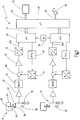
- Fig. 1 an embodiment of the new circuit arrangement is designated in its entirety by the reference numeral 10.
- the circuit arrangement 10 is shown here with a first sensor element 12 and a second sensor element 14. Each of these sensor elements has a photodiode 16 and a MOS transistor 18.
- the MOS transistor 18 has a gate 20 and two further terminals 22, 24, which are commonly referred to as source and drain. In the preferred embodiment, the gate terminal 20 and the drain terminal 24 are shorted.
- the source terminal 22 is connected to the cathode of the photodiode 16. Due to this arrangement, charge carriers, which are generated in the region of the pn junction of the photodiode 16 by impinging electromagnetic radiation 28, 30, flow through the channel 26 of the MOS transistor 18, and the MOS transistor 18 generates an output voltage whose level is logarithmic depends on the intensity of the electromagnetic radiation.
- the sensor elements 12, 14 are shown simplified here. Further advantageous details are in DE 42 09 536 A1 which discloses the basic principle of the logarithmic image cells marketed by the assignee of the present invention under the name HDRC®. In the preferred embodiments of the present invention, all sensor elements are constructed according to this HDRC® principle. In principle, however, the sensor elements can also be applied to others Be implemented manner, for example as a linear CMOS image cells or as CCD image cells.
- Fig. 1 only two sensor elements 12, 14 are shown. However, in preferred embodiments, the new circuitry 10 has a plurality of first and second sensor elements 12, 14 incorporated in FIG Fig. 1 for the sake of simplicity are not shown.
- the plurality of sensor elements 12, 14 is arranged in preferred embodiments on a semiconductor substrate, as described below with reference to FIGS Fig. 2 to 4 is explained.
- an impedance converter 32 is arranged, the output of which is connected to a multiplexer 34.
- a multiplexer 34 With the aid of the multiplexer 34, it is possible to supply a plurality of electrical signals to a common signal processing circuit.
- the in Fig. 1 1 a first multiplexer 34 is used to merge the electrical signals of the first sensor elements 12, while a second multiplexer is used to merge the electrical signals of the second sensor elements 14.
- the new circuit arrangement 10 has two parallel signal processing channels, wherein one signal processing channel processes the electrical signals of the first sensor elements 12, while the other signal processing channel processes the electrical signals of the sensor elements 14.
- the two signal processing channels have the same structure, which is why only the signal processing channel for the first sensor elements 12 is explained in more detail below.
- the output of the multiplexer 34 is connected to an adder 36.
- the adder 36 receives from a D / A converter 38, another electrical signal which is used in a conventional manner for the correction of fixed pattern noise.
- Fixed pattern noise refers to image noise that can occur in an image sensor with a large number of sensor elements, because the electrical properties of the individual sensor elements can vary due to manufacturing tolerances.
- the Fixed Pattern Noise can be corrected by adding in each case an individual correction signal to the electrical signals of the individual sensor elements.
- the correction signal is selected so that the electrical properties of the individual sensor elements are matched to one another.
- Correction coefficients for generating these correction signals are stored here in a memory 40, which is connected to a D / A converter 38.
- the D / A converter 38 uses the correction coefficients from the memory 40 to generate the correction signals for each sensor element.
- the output of the adder 36 is connected via an amplifier 42 to an A / D converter 44, which converts the corrected analog signals of the individual sensor elements into corresponding digital signals 45.
- the digital signals 45 are supplied to a microcontroller 46.
- a microcontroller it is also possible to use an ASIC, an FPGA or another signal processing circuit.
- the microcontroller 46 also serves here to write the correction coefficients for the FPN correction in the memory 40.
- the microcontroller 46 is connected here via an interface 47 to a processor 48.
- the processor 48 receives the electrical signals 45 of all first and second sensor elements 12, 14 and calculates therefrom inter alia temperature values according to the known quotient method.
- the processor 48 provides digital signals for display on a display 52.
- the screen 52 serves to display an optical image of the viewed scene in the visible wavelength range.
- the processor 48 provides signals representing the calculated temperatures.
- the output 54 may be connected to another display 56. Alternatively, the image data and temperature values may also be displayed alternately or together on the screen 52.
- the reference numeral 58 denotes a further temperature-sensitive sensor element, which is shielded in preferred embodiments against electromagnetic radiation 28, 30.
- the first and second sensor elements 12, 14 are image cells (pixels) of a matrix image sensor
- the further sensor element 58 is realized in the form of one or more diodes which are arranged in the edge region of the photosensitive surface of the sensor.
- the further sensor element 58 generates temperature information that is representative of the sensor's own temperature. This temperature information is used in preferred embodiments of the new circuitry by the controllers 46 to computationally correct the electrical signals 45 of the individual sensor elements 12, 14 such that signal variations due to temperature drift of the individual sensor elements are compensated.
- the first and second sensor elements 12, 14 are designed to receive electromagnetic radiation 28, 30 from different wavelength ranges.
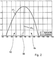
- the first sensor elements 12 are configured to receive electromagnetic radiation 28 from a first wavelength range 62 shown in the diagram in FIG Fig. 2 is shown by a solid line.
- the first wavelength range 62 includes wavelengths from about 280 nm to about 1000 nm. The maximum transmission of this first wavelength range is about 680 nm.
- Such a transmission characteristic of the first sensor elements results when the photodiodes 16 of the first sensor elements 12 are close to the surface Pn junctions are realized in a silicon semiconductor material.
- these limits are not exactly defined, but depend on the materials and process conditions used.
- the first wavelength range 62 is the wavelength range resulting from the spectral sensitivity of silicon photodiodes realized without special filters.
- the second sensor elements 14 are configured to receive electromagnetic radiation 30 from a second wavelength range 64, which is different from the first wavelength range 62.
- the second wavelength range is the "upper half" of the first wavelength range 62.
- the second wavelength range 64 results in the preferred one Embodiments in that the photodiodes of the second sensor elements 14 are provided with an additional edge filter whose transmission characteristic in Fig. 2 is shown at the dotted line 66.
- the transmission jump (cut on) is approximately 680 nm here. Electromagnetic radiation with wavelengths below 680 nm is suppressed by the edge filter. Only electromagnetic radiation with wavelengths above about 680 nm reaches the photodiodes of the second sensor elements 14.
- Fig. 3 shows a first embodiment for the realization of the sensor elements 12, 14.
- Like reference numerals denote the same elements as before.
- Fig. 3 shows a section of a semiconductor substrate 70, which is shown in cross section.
- the semiconductor substrate 70 here is a p-doped silicon substrate or a p-doped well in a semiconductor substrate.
- n-doped islands 72 are arranged in the p-doped substrate 70 .
- another p-doped layer 74 is disposed in the p-doped substrate 70 .
- the pn junction 76 forms the photodiode 16 of the first sensor element 12, while the pn junction 78 forms the photodiode 16 of the second sensor element 14.
- the longer wavelength radiation 30 penetrates deeper into the semiconductor material and thus reaches the deeper pn junction 78, while the shorter wavelength radiation 28 only reaches the upper pn junction 76.
- the layers of the upper pn junction 76 form a filter for the lower pn junction 78.
- the position of the pn junctions 76, 78 is chosen here as a function of the penetration depth of the radiation to be detected.
- a plurality of such stacked photodiodes are arranged side by side in the semiconductor substrate 70.
- the sensor elements 12, 14 together form the individual pixels of the matrix sensor. It is understood that each pixel also includes the MOS transistors and, in preferred embodiments, other devices such as the impedance converter 32. These further components are not shown here for the sake of simplicity.
- Fig. 4 shows a further embodiment, as stacked first and second sensor elements 12, 14 can be realized.
- the sensor elements 12, 14 are realized on an n-doped substrate 70 'by way of example.
- a plurality of self-conductive layers 80 are disposed, over which p-doped layers 82 are located.
- a multiplicity of pin diodes 84 are formed which serve as photodiodes for the second sensor elements 14.
- a continuous insulating layer 85 of silicon dioxide is arranged over the pin diodes 84.
- a plurality of further pin diodes with a layer sequence of n-doped silicon 86, self-conducting silicon 88 and p-doped silicon 90 is arranged on the insulation layer 85.
- the pin diodes with the layer sequence 86, 88, 90 form the first sensor elements 12.
- the layers 86, 88, 90 are produced by means of a CVD method.
- a realization according to the embodiment in Fig. 4 has the advantage that the photodiodes of the sensor elements 12, 14 are stacked on top of each other, but are electrically separated from each other by the insulating layer 85.
- the photodiodes of the two sensor elements 12, 14 are potential-free through the insulation and can therefore be interconnected as desired.
- the islands 72 in the embodiment form according to FIG Fig. 3 a common cathode terminal of the two photodiodes for the sensor elements 12, 14th
- Fig. 5 shows a further embodiment in which the photodiodes of the sensor elements 12, 14 are not arranged vertically one above the other, but horizontally next to each other.
- the photodiodes of the sensor elements 12, 14 are constructed substantially identical.
- these are again pin photodiodes with layers 80, 82 which are arranged in an n-doped silicon substrate 70 "In order to achieve the different spectral sensitivities, a filter 92 is provided above the photodiodes for the second sensor elements 14 arranged, the filter characteristic of the dotted line 66 from Fig. 2 equivalent.
- the filter 92 is implemented as a dielectric interference filter and has an upper layer 94 of silicon nitride, a middle layer 96 of silicon, and a lower layer 98 of silicon nitride.
- the Layers 94 to 98 can in turn be produced by means of a CVD method.
- the sensor elements 12, 14 may be alternately arranged on the surface of the semiconductor substrate 70 'in the manner of a checkerboard pattern or line by line or in columns. Compared to a sensor according to the embodiments according to 3 or 4 the resolution is lower. Each sensor element 12, 14 here forms a separate pixel of the matrix sensor. On the other hand, the sensor elements 12, 14 can be produced here in common process steps. At the end of the process sequence, it is sufficient if the photodiodes of the second sensor elements 14 are covered with the layers 94 to 98.
Description
Die vorliegende Erfindung betrifft eine Schaltungsanordnung zum Erzeugen von licht- und temperaturabhängigen Signalen, die Eigenschaften einer Szene repräsentieren, mit Sensorelementen, die in Abhängigkeit von auftreffender elektromagnetischer Strahlung eine Anzahl von ersten und zweiten elektrischen Signalen erzeugen, wobei die ersten elektrischen Signale in Abhängigkeit von elektromagnetischer Strahlung aus einem ersten Wellenlängenbereich erzeugt sind, der zumindest einen großen Teil des sichtbaren Lichts enthält, und wobei die zweiten elektrischen Signale in Abhängigkeit von elektromagnetischer Strahlung aus einem zweiten Wellenlängenbereich erzeugt sind, der überwiegend Infrarotstrahlung enthält, wobei der erste Wellenlängenbereich den zweiten Wellenlängenbereich überlappt und somit ebenfalls Infrarotstrahlung enthält.The present invention relates to a circuit arrangement for generating light- and temperature-dependent signals representing properties of a scene, with sensor elements which generate a number of first and second electrical signals in response to incident electromagnetic radiation, wherein the first electrical signals in response to electromagnetic Radiation from a first wavelength range are generated, which contains at least a large portion of the visible light, and wherein the second electrical signals are generated in response to electromagnetic radiation from a second wavelength range containing predominantly infrared radiation, wherein the first wavelength range overlaps the second wavelength range and thus also contains infrared radiation.
Eine solche Schaltungsanordnung ist aus
Der bekannte Sensor besitzt also drei verschiedene Arten von Sensorelementen, die auf zumindest teilweise unterschiedliche Prozessschritte hergestellt und auf der Oberfläche des Sensors verteilt werden müssen. Infolgedessen ist die Herstellung des bekannten Sensors recht aufwändig und teuer. Andererseits ist die Auflösung des bekannten Sensors sowohl in Bezug auf das visuelle Bild als auch in Bezug auf die Temperaturverteilung begrenzt, weil die verschiedenen Sensorelemente nebeneinander auf der Oberfläche des Sensors angeordnet sind, so dass zwischen zwei Sensorelementen gleichen Typs jeweils "Lücken" bestehen, die von Sensorelementen eines anderen Typs belegt sind. Die begrenzte Auflösung ist von Nachteil, wenn man beispielsweise anhand des optischen Bildes geometrische Eigenschaften eines aufgenommenen Objekts bestimmen möchte. Schließlich ist auch der Dynamikbereich der Sensorelemente bei dem bekannten Sensor begrenzt, so dass in Abhängigkeit von den Temperaturen und Strahlungsstärken in der beobachteten Szene unterschiedliche Belichtungszeiten benötigt werden. Infolgedessen kann die Bildaufnahme problematisch sein.The known sensor thus has three different types of sensor elements, which must be manufactured on at least partially different process steps and distributed on the surface of the sensor. As a result, the production of the known sensor is quite complex and expensive. On the other hand, the resolution of the known sensor is limited both with respect to the visual image and with respect to the temperature distribution, because the various sensor elements are arranged side by side on the surface of the sensor, so that there are "gaps" between two sensor elements of the same type occupied by sensor elements of a different type. The limited resolution is disadvantageous if one For example, it would like to determine geometric properties of a recorded object on the basis of the optical image. Finally, the dynamic range of the sensor elements is limited in the known sensor, so that depending on the temperatures and radiation levels in the observed scene different exposure times are needed. As a result, image capture can be problematic.
Die bereits zitierte
Quotientenpyrometer sind darüber hinaus seit vielen Jahren aus verschiedenen Druckschriften bekannt. Beispielsweise sei auf
Aus
Aus
Aus
Vor dem Hintergrund dieses Standes der Technik ist es eine Aufgabe der vorliegenden Erfindung, eine Schaltungsanordnung zum Erzeugen von licht- und temperaturabhängigen Signalen anzugeben, mit deren Hilfe sich verschiedene Eigenschaften oder Merkmale von Objekten in einer Szene einschließlich strahlungsabhängiger Eigenschaften mit hoher Genauigkeit und auf kostengünstige Weise bestimmen lassen. Es ist insbesondere eine Aufgabe der Erfindung, eine Schaltungsanordnung anzugeben, mit der sich ein bildgebendes Pyrometer kostengünstig realisieren lässt.Against the background of this prior art, it is an object of the present invention to provide a circuit arrangement for generating light and temperature dependent signals, with the help of various properties or features of objects in a scene including radiation-dependent properties with high accuracy and in a cost effective manner let determine. It is a particular object of the invention to provide a circuit arrangement with which an imaging pyrometer can be realized inexpensively.
Gemäß einem Aspekt der Erfindung wird diese Aufgabe durch eine Schaltungsanordnung der eingangs genannten Art gelöst, wobei die Sensorelemente eine Anzahl von ersten und zweiten Sensorelementen enthalten, wobei die ersten und zweiten Sensorelemente zwei verschiedene Arten von Sensorelementen sind, da sie zur Aufnahme von elektromagnetischer Strahlung aus verschiedenen Wellenlängenbereichen ausgebildet sind, wobei der erste Wellenlängenbereich den zweiten Wellenlängenbereich weitgehend vollständig überlappt, wobei das zweite Sensorelement ein Kantenfilter beinhaltet, das eine untere Grenze des zweiten Wellenlängenbereichs definiert, und wobei die untere Grenze im Wesentlichen mittig zu dem ersten Wellenlängenbereich liegt.According to one aspect of the invention, this object is achieved by a circuit arrangement of the aforementioned type, wherein the sensor elements include a number of first and second sensor elements, wherein the first and second sensor elements are two different types of sensor elements, since they are for receiving electromagnetic radiation wherein the first wavelength range substantially completely overlaps the second wavelength range, wherein the second sensor element includes an edge filter defining a lower limit of the second wavelength range, and wherein the lower limit is substantially centered to the first wavelength range.
Die neue Schaltungsanordnung basiert auf dem an sich bekannten Konzept, elektromagnetische Strahlung aus zwei verschiedenen Wellenlängenbereichen aufzunehmen. Durch eine Quotientenbildung lässt sich dann die Oberflächentemperatur von Objekten in der beobachteten Szene bestimmen. Aufgrund der Quotientenbildung werden die Emissionseigenschaften der Oberfläche eliminiert. Im Gegensatz zu zahlreichen Schaltungsanordnungen aus dem Stand der Technik verwendet die neue Schaltungsanordnung jedoch zwei breitbandige Wellenlängenbereiche, die sich im Bereich der Infrarotstrahlung überlappen. Außerdem enthält der erste Wellenlängenbereich auch einen großen Teil des sichtbaren Lichts. Wie sich überraschend gezeigt hat, ist trotz der im Infrarotbereich überlappenden Wellenlängenbereiche eine Temperaturbestimmung nach dem bekannten Quotientenverfahren mit hoher Genauigkeit möglich. Zusätzlich liefert die neue Schaltungsanordnung auch Signale aus dem sichtbaren Wellenlängenbereich. Daher ermöglicht die neue Schaltungsanordnung nicht nur eine Temperaturbestimmung, sondern sie liefert auch Signale für die Erzeugung eines optischen Bildes (herkömmliches Kamerabild) der beobachteten Szene.The new circuit arrangement is based on the known concept of receiving electromagnetic radiation from two different wavelength ranges. A quotient can then be used to determine the surface temperature of objects in the observed scene. Due to the quotient formation, the emission properties of the surface are eliminated. However, unlike many prior art circuit arrangements, the new circuitry uses two broadband wavelength ranges that overlap in the infrared radiation range. In addition, the first wavelength range also contains a large portion of the visible light. As has surprisingly been found, a temperature determination according to the known quotient method with high accuracy is possible in spite of the wavelength ranges overlapping in the infrared range. In addition, the new circuitry also provides signals from the visible wavelength range. Therefore, the new circuitry not only enables temperature determination but also provides signals for the generation of an optical image (conventional camera image) of the observed scene.
Im Gegensatz zu der eingangs genannten Schaltungsanordnung nach
Da lediglich zwei verschiedene Arten von Sensorelementen benötigt werden, können Sensorelemente gleichen Typs auf der Oberfläche eines matrixartigen Bildsensors dichter nebeneinander angeordnet werden, was eine höhere Auflösung ermöglicht. Infolgedessen lassen sich geometrische Eigenschaften eines beobachteten Objekts aus den aufgenommenen Bildern mit höherer Genauigkeit bestimmen. Prinzipiell kann die neue Schaltungsanordnung jedoch nicht nur bei matrixartigen Bildsensoren eingesetzt werden, sondern auch bei Pyrometern, die lediglich zwei Sensorelemente oder eine geringe Anzahl von ersten und zweiten Sensorelementen besitzen.Since only two different types of sensor elements are needed, sensor elements of the same type can be arranged closer together on the surface of a matrix-type image sensor, which enables a higher resolution. As a result, geometrical properties of an observed object can be determined from the acquired images with higher accuracy. In principle, however, the new circuit arrangement can be used not only with matrix-type image sensors but also with pyrometers having only two sensor elements or a small number of first and second sensor elements.
Außerdem ist der zweite Wellenlängenbereich ein Teilbereich des ersten Wellenlängenbereichs. Diese Ausgestaltung ermöglicht eine sehr einfache und kostengünstige Realisierung der ersten und zweiten Sensorelemente, da die beiden Sensorelemente prinzipiell identisch aufgebaut sein können und sich nur durch ein oder mehrere zusätzliche Filter für die zweiten Sensorelemente voneinander unterscheiden.In addition, the second wavelength range is a partial range of the first wavelength range. This embodiment allows a very simple and cost-effective implementation of the first and second sensor elements, since the two sensor elements can be constructed identically in principle and differ from each other only by one or more additional filters for the second sensor elements.
Für die Temperaturbestimmung nach dem Quotientenverfahren macht sich die neue Schaltungsanordnung zunutze, dass der erste und der zweite Wellenlängenbereich, die mit den ersten und zweiten Sensorelementen aufgenommen werden, verschieden voneinander sind. Infolgedessen liefern die ersten und zweiten Sensorelemente unterschiedliche elektrische Signale, selbst wenn sie auf ein und denselben Punkt innerhalb der beobachteten Szene ausgerichtet sind. Die unterschiedlichen Signale ermöglichen die Temperaturbestimmung nach dem Quotientenverfahren, obwohl der erste und der zweite Wellenlängenbereich im Bereich der Infrarotstrahlung überlappen.For the temperature determination according to the quotient method, the new circuit arrangement makes use of the fact that the first and the second wavelength range, which are recorded with the first and second sensor elements, are different from one another. As a result, the first and second sensor elements provide different electrical signals, even if they are aligned to one and the same point within the observed scene. The different signals allow the temperature determination by the quotient method, although the first and the second wavelength range in the range of infrared radiation overlap.
Ein Kantenfilter im Sinne dieser Ausgestaltung ist ein Filter, das einen Transmissionssprung verursacht, der die untere Grenze des zweiten Wellenlängenbereichs definiert. Vorzugsweise liegt die untere Grenze zwischen etwa 660 nm und etwa 740 nm, vorzugsweise zwischen etwa 680 nm und etwa 720 nm, und besonders bevorzugt im Bereich von etwa 700 nm. Die angegebenen Wellenlängen und Wellenlängenbereiche sind bevorzugt, weil sie sich einerseits kostengünstig realisieren lassen und andererseits gute Messergebnisse insbesondere für die Temperaturbestimmung liefern. Die Verwendung eines Kantenfilters ermöglicht eine sehr einfache und kostengünstige Realisierung der zweiten Sensorelemente auf demselben Halbleitersubstrat, auf dem die ersten Sensorelemente angeordnet sind.An edge filter in the sense of this embodiment is a filter that causes a transmittance jump that defines the lower limit of the second wavelength range. Preferably, the lower limit is between about 660 nm and about 740 nm, preferably between about 680 nm and about 720 nm, and more preferably in the range of about 700 nm. The stated wavelengths and wavelength ranges are preferred because they can be realized on the one hand cost and on the other hand good measurement results, especially for temperature determination deliver. The use of an edge filter enables a very simple and cost-effective implementation of the second sensor elements on the same semiconductor substrate on which the first sensor elements are arranged.
Die untere Grenze liegt im Wesentlichen mittig zu dem ersten Wellenlängenbereich. Dies trägt zu einer einfachen und kostengünstigen Herstellung der neuen Schaltungsanordnung bei. Außerdem lassen sich mit dieser Ausgestaltung sehr gute Messergebnisse erreichen. Von Vorteil ist hier, dass sich die Energieverteilungen in den beiden gebildeten Wellenlängenbereichen sehr gut für die Quotientenbildung eignen, da die detektierbaren Energien bei höheren Wellenlängen zunehmen.The lower limit lies substantially in the middle of the first wavelength range. This contributes to a simple and inexpensive production of the new circuit arrangement. In addition, very good measurement results can be achieved with this embodiment. The advantage here is that the energy distributions in the two wavelength ranges formed are very well suited for quotient formation, since the detectable energies increase at higher wavelengths.
Die oben genannte Aufgabe ist daher vollständig gelöst.The above object is therefore completely solved.
In einer bevorzugten Ausgestaltung besitzt die neue Schaltungsanordnung einen Schaltungsteil, der dazu ausgebildet ist, eine Temperatur der Szene in Abhängigkeit von den ersten und zweiten Signalen zu bestimmen.In a preferred embodiment, the new circuit arrangement has a circuit part which is designed to determine a temperature of the scene as a function of the first and second signals.
In dieser Ausgestaltung erhält der Schaltungsteil die ersten und zweiten elektrischen Signale und er führt eine Quotientenbildung durch, um Emissionseigenschaften von Oberflächen in der beobachteten Szene zu eliminieren. Dieses an sich bekannte Verfahren zur Bestimmung der Temperatur einer strahlenden Oberfläche lässt sich mit der neuen Schaltungsanordnung in sehr einfacher und kostengünstiger Weise realisieren. In der bevorzugten Ausgestaltung ist der Schaltungsteil zur Bestimmung der Temperatur ein Teil der neuen Schaltungsanordnung. Alternativ hierzu könnte die neue Schaltungsanordnung jedoch auch separat von dem Schaltungsteil verwendet werden, beispielsweise zur zeitgleichen Aufnahme von visuellen Bildern und Infrarotbildern.In this embodiment, the circuit portion receives the first and second electrical signals and performs quotient formation to eliminate emission characteristics of surfaces in the observed scene. This known method for determining the temperature of a radiating surface can be realized with the new circuit arrangement in a very simple and cost-effective manner. In the preferred embodiment, the circuit part is for determination the temperature is part of the new circuitry. Alternatively, however, the new circuit arrangement could also be used separately from the circuit part, for example for the simultaneous recording of visual images and infrared images.
In einer weiteren Ausgestaltung beinhaltet die neue Schaltungsanordnung ein Halbleitersubstrat, auf dem eine Vielzahl von ersten und zweiten Sensorelementen nebeneinander angeordnet sind.In a further embodiment, the new circuit arrangement includes a semiconductor substrate on which a multiplicity of first and second sensor elements are arranged next to one another.
Vorzugsweise sind die ersten und zweiten Sensorelemente matrixartig nebeneinander angeordnet. Sie bilden einen flächigen Bildsensor mit einer Vielzahl von Pixeln. Die ersten und zweiten Sensorelemente können abwechselnd nach Art eines Schachbrettmusters an der Oberfläche des Halbleitersubstrats angeordnet sein. In anderen Ausführungsbeispielen wechseln sich die ersten und zweiten Sensorelemente zeilen- oder spaltenweise ab. Diese Ausgestaltungen ermöglichen eine schnelle und zeitsynchrone Aufnahme von flächigen Bildern einer beobachteten Szene sowohl im Bereich des sichtbaren Lichts als auch im Infrarotbereich. Durch die zeitsynchrone Aufnahme ist eine gute Zuordnung der verschiedenen Bilder zueinander möglich.Preferably, the first and second sensor elements are arranged next to one another like a matrix. They form a flat image sensor with a plurality of pixels. The first and second sensor elements may be arranged alternately in the manner of a checkerboard pattern on the surface of the semiconductor substrate. In other embodiments, the first and second sensor elements alternate in rows or columns. These embodiments allow a fast and time-synchronized recording of areal images of an observed scene both in the visible light and in the infrared range. Due to the time-synchronized recording a good assignment of the different images is possible.
In einer weiteren Ausgestaltung sind die ersten und zweiten Sensorelemente jeweils übereinander angeordnet.In a further embodiment, the first and second sensor elements are arranged one above the other.
Diese Ausgestaltung kann die neue Schaltungsanordnung für sich genommen weiterbilden, aber auch in Kombination mit der vorhergehenden Ausgestaltung sehr vorteilhaft verwendet werden. Im erstgenannten Fall besitzt die neue Schaltungsanordnung lediglich ein oder wenige erste und zweite Sensorelemente, die beispielsweise für eine punktuelle, selektive Messung in einer Szene verwendet werden können. Im zweiten Fall sind eine Vielzahl von ersten und zweiten Sensorelementen, die jeweils stapelweise übereinander angeordnet sind, matrixartig nebeneinander angeordnet. Jedes Paar aus erstem und zweitem Sensorelement bildet hier gemeinsam ein Pixel des Matrixsensors. Die zuletzt genannte Ausgestaltung ermöglicht eine sehr hohe Auflösung. Von Vorteil ist, dass die Materiallagen, die das oben liegende Sensorelement jedes Stapels bilden, bereits eine Filterwirkung in Bezug auf die Strahlung haben, die das unten liegende Sensorelement erreicht. Außerdem können alle Sensorelemente in gemeinsamen Prozessschritten hergestellt werden, was die Herstellung der neuen Schaltungsanordnung insgesamt vereinfacht. Aber auch wenn die neue Schaltungsanordnung nicht für einen Matrixsensor verwendet wird, ermöglicht diese Ausgestaltung einen sehr kleinen Sensor, mit dem die ersten und zweiten Sensorelemente auf identische Messpunkte innerhalb der beobachteten Szene ausgerichtet werden können.This embodiment can further develop the new circuit arrangement per se, but can also be used very advantageously in combination with the preceding embodiment. In the former case, the new circuit arrangement has only one or a few first and second sensor elements that can be used, for example, for a punctual, selective measurement in a scene. In the second case, a plurality of first and second sensor elements, which are each stacked one above the other, arranged in a matrix-like manner next to one another. Each pair of first and second sensor element together forms a pixel of the matrix sensor. The latter embodiment allows a very high resolution. It is advantageous that the layers of material that form the upper sensor element of each stack already have a filtering effect with respect to the radiation that reaches the lower sensor element. In addition, all sensor elements can be produced in common process steps, which simplifies the production of the new circuit arrangement as a whole. However, even if the new circuit arrangement is not used for a matrix sensor, this embodiment allows a very small sensor, with which the first and second sensor elements can be aligned to identical measuring points within the observed scene.
In einer weiteren bevorzugten Ausgestaltung beinhalten die ersten und zweiten Sensorelemente jeweils eine Photodiode und zumindest einen MOS-Transistor mit einem Gateanschluss, zwei weiteren Anschlüssen und einem Kanal, wobei die Photodiode mit dem MOS-Transistor so gekoppelt ist, dass in der Photodiode generierte Ladungsträger durch den Kanal abfließen, und wobei der Gateanschluss mit einem der zwei weiteren Anschlüsse leitend verbunden ist.In a further preferred embodiment, the first and second sensor elements each include a photodiode and at least one MOS transistor having a gate terminal, two further terminals and a channel, wherein the photodiode is coupled to the MOS transistor so that in the photodiode generated by charge carriers drain the channel, and wherein the gate terminal is conductively connected to one of the two other terminals.
In dieser Ausgestaltung sind die ersten und zweiten Sensorelemente insbesondere nach dem HDRC-Prinzip aufgebaut, wie es in der eingangs genannten
In einer weiteren Ausgestaltung ist das Kantenfilter ein dielektrisches Interferenzfilter mit einer Vielzahl von übereinander angeordneten Materiallagen, wobei diese Materiallagen im Wesentlichen aus Silizium und Siliziumnitrid gebildet sind. In einem bevorzugten Ausführungsbeispiel besteht das Interferenzfilter aus zwei Siliziumnitridschichten, zwischen denen eine Siliziumschicht angeordnet ist.In a further refinement, the edge filter is a dielectric interference filter having a multiplicity of material layers arranged one above the other, wherein these material layers are essentially formed from silicon and silicon nitride. In a preferred embodiment, the interference filter consists of two silicon nitride layers, between which a silicon layer is arranged.
Diese Ausgestaltung ermöglicht eine sehr einfache und kostengünstige Herstellung des Interferenzfilters innerhalb einer Prozessfolge, mit der auch die ersten und zweiten Sensorelemente auf einem Halbleitersubstrat hergestellt werden. Ein Kantenfilter mit der angegebenen Schichtfolge aus Siliziumnitrid und Silizium lässt sich sehr einfach und kostengünstig herstellen und hat in Ausführungsbeispielen der Erfindung sehr gute Messergebnisse ermöglicht.This refinement enables a very simple and cost-effective production of the interference filter within a process sequence, with which the first and second sensor elements are also produced on a semiconductor substrate. An edge filter with the specified layer sequence of silicon nitride and silicon can be produced in a very simple and cost-effective manner and has enabled very good measurement results in embodiments of the invention.
In einer weiteren Ausgestaltung besitzt die neue Schaltungsanordnung zumindest ein weiteres temperaturempfindliches Sensorelement, das gegen die elektromagnetische Strahlung aus dem ersten und zweiten Wellenlängenbereich abgeschirmt ist.In a further embodiment, the new circuit arrangement has at least one further temperature-sensitive sensor element which is shielded from the electromagnetic radiation from the first and second wavelength ranges.
In bevorzugten Ausführungsbeispielen ist das weitere temperaturempfindliche Sensorelement eine Diode, die von einem Messstrom durchflossen ist. Das temperaturempfindliche Verhalten dieser Diode ermöglicht es, eine temperaturabhängige Drift der ersten und zweiten Sensorelemente zu korrigieren, indem die ersten und zweiten Signale in Bezug auf die Temperatur kalibriert werden. Besonders vorteilhaft ist es, wenn das weitere temperaturempfindliche Sensorelement mit Hilfe von einer oder mehreren Dioden realisiert wird, die häufig als so genannte Prozesskontrollstrukturen im Randbereich eines Bildsensors vorhanden sind. Es genügt, wenn man über einer solchen Prozesskontrollstruktur Materiallagen anordnet, die die elektromagnetische Strahlung aus dem ersten und zweiten Wellenlängenbereich abschirmen, wie etwa eine Metallisierung. In bevorzugten Ausführungsbeispielen wird die Temperaturkompensation der ersten und zweiten Signale in gleicher Weise durchgeführt, wie eine FPN-(Fixed Pattern Noise)Korrektur bei einem Bildsensor mit einer Vielzahl von matrixartig nebeneinander angeordneten Sensorelementen. Diese Ausgestaltung ermöglicht sehr hohe Messgenauigkeiten bei der Temperaturmessung.In preferred exemplary embodiments, the further temperature-sensitive sensor element is a diode through which a measuring current flows. The temperature-sensitive behavior of this diode makes it possible to correct a temperature-dependent drift of the first and second sensor elements by calibrating the first and second signals with respect to the temperature. It is particularly advantageous if the further temperature-sensitive sensor element is realized with the aid of one or more diodes, which are frequently present as so-called process control structures in the edge region of an image sensor. It suffices to arrange material layers over such a process control structure which shield the electromagnetic radiation from the first and second wavelength ranges, such as a metallization. In preferred embodiments, the temperature compensation of the first and second signals is performed in the same way as an FPN (Fixed Pattern Noise) correction in an image sensor with a plurality of matrix-like juxtaposed sensor elements. This embodiment allows very high measurement accuracy in the temperature measurement.
Es versteht sich, dass die vorstehend genannten und die nachstehend noch zu erläuternden Merkmale nicht nur in der jeweils angegebenen Kombination, sondern auch in anderen Kombinationen oder in Alleinstellung verwendbar sind, ohne den Rahmen der vorliegenden Erfindung zu verlassen.It is understood that the features mentioned above and those yet to be explained below can be used not only in the particular combination given, but also in other combinations or in isolation, without departing from the scope of the present invention.
Ausführungsbeispiele der Erfindung sind in der Zeichnung dargestellt und werden in der nachfolgenden Beschreibung näher erläutert. Es zeigen:
- Fig. 1
- eine schematische Darstellung eines Ausführungsbeispiels der neuen Schaltungsanordnung,
- Fig. 2
- ein Spektraldiagramm zur Erläuterung von bevorzugten Ausführungsbeispielen der neuen Schaltungsanordnung,
- Fig. 3
- ein erstes Ausführungsbeispiel zur Realisierung der ersten und zweiten Sensorelemente,
- Fig. 4
- ein weiteres Ausführungsbeispiel zur Realisierung der ersten und zweiten Sensorelemente, und
- Fig. 5
- noch ein weiteres Ausführungsbeispiel zur Realisierung der ersten und zweiten Sensorelemente.
- Fig. 1
- a schematic representation of an embodiment of the new circuit arrangement,
- Fig. 2
- a spectral diagram for explaining preferred embodiments of the new circuit arrangement,
- Fig. 3
- a first embodiment for the realization of the first and second sensor elements,
- Fig. 4
- a further embodiment for the realization of the first and second sensor elements, and
- Fig. 5
- Yet another embodiment for the realization of the first and second sensor elements.
In
Die Schaltungsanordnung 10 ist hier mit einem ersten Sensorelement 12 und einem zweiten Sensorelement 14 dargestellt. Jedes dieser Sensorelemente besitzt eine Photodiode 16 und einen MOS-Transistor 18. Der MOS-Transistor 18 besitzt ein Gate 20 und zwei weitere Anschlüsse 22, 24, die üblicherweise als Source und als Drain bezeichnet werden. Im bevorzugten Ausführungsbeispiel sind der Gateanschluss 20 und der Drainanschluss 24 kurzgeschlossen. Der Sourceanschluss 22 ist mit der Kathode der Photodiode 16 verbunden. Aufgrund dieser Anordnung fließen Ladungsträger, die im Bereich des pn-Übergangs der Photodiode 16 durch auftreffende elektromagnetische Strahlung 28, 30 erzeugt werden, durch den Kanal 26 des MOS-Transistors 18 ab, und der MOS-Transistor 18 erzeugt eine Ausgangsspannung, deren Höhe logarithmisch von der Intensität der elektromagnetischer Strahlung abhängt.The
Die Sensorelemente 12, 14 sind hier vereinfacht dargestellt. Weitere vorteilhafte Details sind in
In
In dem Ausführungsbeispiel gemäß
Der Ausgang des Multiplexers 34 ist mit einem Addierer 36 verbunden. Der Addierer 36 erhält von einem D/A-Wandler 38 ein weiteres elektrisches Signal, das in an sich bekannter Weise zur Korrektur von Fixed Pattern Noise dient. Fixed Pattern Noise bezeichnet ein Bildrauschen, das bei einem Bildsensor mit einer Vielzahl von Sensorelementen auftreten kann, weil die elektrischen Eigenschaften der einzelnen Sensorelemente aufgrund von Fertigungstoleranzen variieren können. Das Fixed Pattern Noise lässt sich korrigieren, indem man jeweils ein individuelles Korrektursignal zu den elektrischen Signalen der einzelnen Sensorelemente addiert. Das Korrektursignal ist so ausgewählt, dass die elektrischen Eigenschaften der einzelnen Sensorelemente aneinander angeglichen werden. Korrekturkoeffizienten zum Erzeugen dieser Korrektursignale sind hier in einem Speicher 40 hinterlegt, der mit einem D/A-Wandler 38 verbunden ist. Der D/A-Wandler 38 erzeugt anhand der Korrekturkoeffizienten aus dem Speicher 40 die Korrektursignale für jedes Sensorelement.The output of the
Der Ausgang des Addierers 36 ist über einen Verstärker 42 mit einem A/D-Wandler 44 verbunden, der die korrigierten analogen Signale der einzelnen Sensorelemente in entsprechende digitale Signale 45 umwandelt. Die digitalen Signale 45 werden einem Mikrocontroller 46 zugeführt. Anstelle eines Mikrocontrollers kann auch ein ASIC, ein FPGA oder ein anderer Signalverarbeitungsschaltkreis verwendet werden. Der Mikrocontroller 46 dient hier auch dazu, die Korrekturkoeffizienten für die FPN-Korrektur in den Speicher 40 zu schreiben.The output of the
Der Mikrocontroller 46 ist hier über eine Schnittstelle 47 mit einem Prozessor 48 verbunden. Der Prozessor 48 erhält die elektrischen Signale 45 aller ersten und zweiten Sensorelemente 12, 14 und berechnet daraus unter anderem Temperaturwerte nach dem bekannten Quotientenverfahren. An einem Ausgang 50 stellt der Prozessor 48 digitale Signale zur Anzeige auf einem Bildschirm 52 zur Verfügung. In bevorzugten Ausführungsbeispielen dient der Bildschirm 52 dazu, ein optisches Bild der betrachteten Szene im sichtbaren Wellenlängenbereich anzuzeigen. An einem Ausgang 54 stellt der Prozessor 48 Signale bereit, die die berechneten Temperaturen repräsentieren. Der Ausgang 54 kann mit einer weiteren Anzeige 56 verbunden sein. Alternativ hierzu können die Bilddaten und Temperaturwerte auch wechselweise oder gemeinsam auf dem Bildschirm 52 angezeigt werden.The
Mit der Bezugsziffer 58 ist ein weiteres temperaturempfindliches Sensorelement bezeichnet, das in bevorzugten Ausführungsbeispielen gegen elektromagnetische Strahlung 28, 30 abgeschirmt ist. Für den Fall, dass die ersten und zweiten Sensorelemente 12, 14 Bildzellen (Pixel) eines Matrix-Bildsensors sind, ist es bevorzugt, wenn das weitere Sensorelement 58 in Form einer oder mehrerer Dioden realisiert ist, die im Randbereich der lichtempfindlichen Fläche des Sensors angeordnet sind. Das weitere Sensorelement 58 erzeugt eine Temperaturinformation, die für die Eigentemperatur des Sensors repräsentativ ist. Diese Temperaturinformation wird in bevorzugten Ausführungsbeispielen der neuen Schaltungsanordnung von den Controllern 46 verwendet, um die elektrischen Signale 45 der einzelnen Sensorelemente 12, 14 rechnerisch so zu korrigieren, dass Signalveränderungen aufgrund von Temperaturdrift der einzelnen Sensorelemente kompensiert sind.The
Entsprechend der bevorzugten Verwendung der neuen Schaltungsanordnung für ein bildgebendes Pyrometer sind die ersten und zweiten Sensorelemente 12, 14 zur Aufnahme von elektromagnetischer Strahlung 28, 30 aus verschiedenen Wellenlängenbereichen ausgebildet. In dem bevorzugten Ausführungsbeispiel sind die ersten Sensorelemente 12 so ausgebildet, dass sie elektromagnetische Strahlung 28 aus einem ersten Wellenlängenbereich 62 aufnehmen, der in dem Diagramm in
Die zweiten Sensorelemente 14 sind dazu ausgebildet, elektromagnetische Strahlung 30 aus einem zweiten Wellenlängenbereich 64 aufzunehmen, der von dem ersten Wellenlängenbereich 62 verschieden ist. In einem bevorzugten Ausführungsbeispiel ist der zweite Wellenlängenbereich die "obere Hälfte" des ersten Wellenlängenbereichs 62. Der zweite Wellenlängenbereich 64 ergibt sich in den bevorzugten Ausführungsbeispielen dadurch, dass die Photodioden der zweiten Sensorelemente 14 mit einem zusätzlichen Kantenfilter versehen sind, dessen Transmissionscharakteristik in
In Ausführungsbeispielen gemäß
Claims (8)
- A circuit arrangement for generating light- and temperature-dependent signals (45) which represent properties of a scene, comprising sensor elements (12, 14), which generate a number of first and second electrical signals (45a, 45b) that are dependent on impinging electromagnetic radiation (28, 30), wherein the first electrical signals (45a) are generated in a manner dependent on electromagnetic radiation (28) from a first wavelength range (62) comprising at least a large part of visible light, and wherein the second electrical signals (45b) are generated in a manner dependent on electromagnetic radiation (30) from a second wavelength range (64) predominantly comprising infrared radiation, wherein the first wavelength range (62) overlaps the second wavelength range (64) and therefore also comprises infrared radiation, characterized in that the sensors elements comprise a number of first (12) and second (14) sensor elements, wherein the first and second sensor elements (12, 14) are of different kind, since they are designed for recording of electromagnetic radiation (28, 30) from different wavelength ranges, wherein the first wavelength range (62) substantially completely overlaps the second wavelength range (64), wherein the second sensor element (14) comprises a cut-off filter (92), which defines a lower limit (66) of the second wavelength range (64), and wherein the lower limit (66) is located substantially centrally with respect to the first wavelength range (62).
- The circuit arrangement of claim 1, characterized by a circuit part (48) designed to determine a temperature of the scene in a manner dependent on the first and second signals (45a, 45b).
- The circuit arrangement of claim 1 or 2, characterized by a semiconductor substrate (70), on which a plurality of first and second sensor elements (12, 14) are arranged side by side.
- The circuit arrangement of any of claims 1 to 3, characterized in that the first and second sensor elements (12, 14) are arranged one above the other.
- The circuit arrangement of any of claims 1 to 4, characterized in that the first and second sensor elements (12,14) each comprise a photodiode (16) and at least one MOS transistor (18) having a gate terminal (20), two further terminals (22, 24) and a channel (26), wherein the photodiode (16) is coupled to the MOS transistor (18) in such a way that charge carriers generated in the photodiode (16) drain into the channel (26), and wherein the gate terminal (20) is conductively connected to one of the two further terminals (24).
- The circuit arrangement of any of claims 1 to 5, characterized in that the cut-off filter (92) is a dielectric interference filter having a plurality of material layers (94-98) arranged one above another, wherein the material layers (94-98) are formed substantially from silicon and silicon nitride.
- The circuit arrangement of any of claims 1 to 6, characterized by at least one further temperature-sensitive sensor element (58), which is shielded from the electromagnetic radiation from the first and second wavelength ranges (62, 64).
- A method of using a circuit arrangement of any of claims 1 to 7 as a pyrometer, in particular as an imaging pyrometer.
Applications Claiming Priority (2)
| Application Number | Priority Date | Filing Date | Title |
|---|---|---|---|
| DE102007054314A DE102007054314A1 (en) | 2007-11-05 | 2007-11-05 | Circuit arrangement for generating light and temperature-dependent signals, in particular for an imaging pyrometer |
| PCT/EP2008/009167 WO2009059721A1 (en) | 2007-11-05 | 2008-10-30 | Circuit arrangement for creating light and temperature dependant signals, particularly for an imaging pyrometer |
Publications (2)
| Publication Number | Publication Date |
|---|---|
| EP2210073A1 EP2210073A1 (en) | 2010-07-28 |
| EP2210073B1 true EP2210073B1 (en) | 2017-05-17 |
Family
ID=40262259
Family Applications (1)
| Application Number | Title | Priority Date | Filing Date |
|---|---|---|---|
| EP08846593.5A Active EP2210073B1 (en) | 2007-11-05 | 2008-10-30 | Circuit arrangement for creating light and temperature dependant signals, particularly for an imaging pyrometer |
Country Status (7)
| Country | Link |
|---|---|
| US (1) | US8309924B2 (en) |
| EP (1) | EP2210073B1 (en) |
| JP (1) | JP2011503560A (en) |
| KR (1) | KR20100084565A (en) |
| CN (1) | CN101910809A (en) |
| DE (1) | DE102007054314A1 (en) |
| WO (1) | WO2009059721A1 (en) |
Families Citing this family (9)
| Publication number | Priority date | Publication date | Assignee | Title |
|---|---|---|---|---|
| JP5768477B2 (en) * | 2011-05-02 | 2015-08-26 | 新日鐵住金株式会社 | Method for measuring temperature of workpiece, method for manufacturing workpiece, and heating device for workpiece |
| DE102012112412A1 (en) * | 2012-12-17 | 2014-06-18 | LumaSense Technologies GmbH | Apparatus and method for measuring a spatially resolved temperature distribution |
| CN106796861B (en) * | 2014-04-17 | 2019-05-03 | 加坦公司 | Mixed tensor conversion and processing detection device |
| US9899550B2 (en) * | 2015-08-12 | 2018-02-20 | Toyota Motor Engineering & Manufacturing North America, Inc. | Electric power transfer system using optical power transfer |
| FR3067167B1 (en) * | 2017-06-06 | 2019-06-28 | Office National D'etudes Et De Recherches Aerospatiales | SPECTRAL CONVERSION ELEMENT FOR ELECTROMAGNETIC RADIATION |
| KR20200066654A (en) | 2017-10-03 | 2020-06-10 | 필립모리스 프로덕츠 에스.에이. | Aerosol-generating devices and systems comprising pyrometers |
| DE102018133518B4 (en) | 2018-12-21 | 2023-07-06 | Bias Bremer Institut Für Angewandte Strahltechnik | Camera to determine a 2D thermal image as well as system and process control equipment |
| CN113049589B (en) * | 2021-03-10 | 2021-12-03 | 清华大学 | Adjustable image acquisition method in high-temperature environment |
| WO2023230102A1 (en) * | 2022-05-27 | 2023-11-30 | Basf Corporation | Pyrometer electronics design for modern industry protocols |
Family Cites Families (19)
| Publication number | Priority date | Publication date | Assignee | Title |
|---|---|---|---|---|
| DE867453C (en) | 1942-12-13 | 1953-02-16 | Siemens Ag | Process for the automatic measurement of the color temperature using photoelectric cells |
| DE1237804B (en) | 1958-04-01 | 1967-03-30 | Shaw Instr Corp | Color pyrometer |
| DE1136135B (en) | 1960-08-29 | 1962-09-06 | Siemens Ag | Color pyrometer with two flat radiation receivers |
| US3435237A (en) | 1965-01-21 | 1969-03-25 | Prd Electronics Inc | Radiation discriminator means |
| US3535237A (en) * | 1967-04-25 | 1970-10-20 | Texaco Inc | Drilling fluid |
| GB1507367A (en) | 1974-06-10 | 1978-04-12 | Siemens Ag | Automatic radiation pyrometer |
| US4413324A (en) | 1981-02-25 | 1983-11-01 | Sumitomo Kinzoku Kogyo Kabushiki Kaisha | Temperature pattern measuring method and a device therefor |
| US4570332A (en) | 1982-05-10 | 1986-02-18 | Sharp Kabushiki Kaisha | Method of forming contact to thin film semiconductor device |
| DE3477963D1 (en) * | 1983-06-16 | 1989-06-01 | Deutsche Forsch Luft Raumfahrt | Method for the contactless radiation measurement of the temperature of an object independent of its emissivity, and device for carrying out this method |
| US4681434A (en) * | 1985-11-14 | 1987-07-21 | United Technologies Corporation | Dual spectra optical pyrometer having a serial array of photodectectors |
| DE4209536C3 (en) | 1992-03-24 | 2000-10-05 | Stuttgart Mikroelektronik | Image cell for an image sensor chip |
| JP2856180B2 (en) * | 1996-11-27 | 1999-02-10 | 日本電気株式会社 | Thermal type infrared detecting element and manufacturing method thereof |
| DE19650705A1 (en) | 1996-12-08 | 1998-06-10 | Robert Prof Dr Ing Massen | Contactless imaging method of radiometric or geometric properties of object or material for optical inspection of products |
| US5963311A (en) * | 1997-09-12 | 1999-10-05 | Stratonics, Inc. | Surface and particle imaging pyrometer and method of use |
| ATE272208T1 (en) | 2000-03-13 | 2004-08-15 | Suisse Electronique Microtech | IMAGING PYROMETER |
| JP4578797B2 (en) | 2003-11-10 | 2010-11-10 | パナソニック株式会社 | Imaging device |
| AT501638A1 (en) * | 2005-04-13 | 2006-10-15 | Ruebig Gmbh & Co Kg | DEVICE FOR TOUCH-FREE TEMPERATURE MEASUREMENT |
| US20070145273A1 (en) * | 2005-12-22 | 2007-06-28 | Chang Edward T | High-sensitivity infrared color camera |
| KR100863497B1 (en) * | 2007-06-19 | 2008-10-14 | 마루엘에스아이 주식회사 | Image sensing apparatus, method for processing image signal, light sensing device, control method, and pixel array |
-
2007
- 2007-11-05 DE DE102007054314A patent/DE102007054314A1/en not_active Withdrawn
-
2008
- 2008-10-30 WO PCT/EP2008/009167 patent/WO2009059721A1/en active Application Filing
- 2008-10-30 CN CN2008801239578A patent/CN101910809A/en active Pending
- 2008-10-30 JP JP2010532478A patent/JP2011503560A/en active Pending
- 2008-10-30 KR KR1020107011629A patent/KR20100084565A/en not_active Application Discontinuation
- 2008-10-30 EP EP08846593.5A patent/EP2210073B1/en active Active
-
2010
- 2010-05-04 US US12/773,349 patent/US8309924B2/en not_active Expired - Fee Related
Also Published As
| Publication number | Publication date |
|---|---|
| US8309924B2 (en) | 2012-11-13 |
| JP2011503560A (en) | 2011-01-27 |
| WO2009059721A1 (en) | 2009-05-14 |
| CN101910809A (en) | 2010-12-08 |
| US20100278212A1 (en) | 2010-11-04 |
| DE102007054314A1 (en) | 2009-05-07 |
| EP2210073A1 (en) | 2010-07-28 |
| KR20100084565A (en) | 2010-07-26 |
Similar Documents
| Publication | Publication Date | Title |
|---|---|---|
| EP2210073B1 (en) | Circuit arrangement for creating light and temperature dependant signals, particularly for an imaging pyrometer | |
| DE19857851B4 (en) | Detection device for physical and / or chemical quantities | |
| DE60031590T2 (en) | image sensor | |
| DE60035580T2 (en) | SEMICONDUCTOR | |
| DE69729648T2 (en) | ACTIVE PIXEL SENSOR MATRIX WITH MULTI-LOAD OUTPUT | |
| DE69528386T2 (en) | PICTURE SYSTEM | |
| DE69826886T2 (en) | OPTOELECTRONIC CAMERA AND METHOD FOR IMAGING | |
| DE69732862T2 (en) | SEMICONDUCTOR ARRANGEMENT FOR RECORDING INFRARED PICTURES | |
| DE3710986C2 (en) | ||
| DE2741226C3 (en) | Solid-state color image pickup device | |
| CN107004685A (en) | Solid photographic device and electronic installation | |
| DE202017102626U1 (en) | Double-photodiode image pixel | |
| DE10153378A1 (en) | Photo sensor system has pairs of arrays for each colour each having large and small range | |
| DE102005005590A1 (en) | Light-filtering image sensor | |
| DE112011106038B4 (en) | Imaging device | |
| EP0343366A1 (en) | Camera | |
| CN107566764A (en) | The photoelectric door and its manufacture method of preceding illuminated infrared image sensor | |
| DE112021004358T5 (en) | SOLID STATE IMAGING DEVICE AND ELECTRONIC DEVICE | |
| DE112019003270T5 (en) | AMBIENT LIGHT DETECTOR, DETECTOR ARRANGEMENT AND PROCEDURES | |
| DE102011053219A1 (en) | Pixels for detecting amplitude and phase of electromagnetic radiation in form of photonic mixer devices, has phase sensitive sub-pixels for detection of incident electromagnetic radiation with photosensitive pixel surface | |
| DE102018132973A1 (en) | Image sensors with calibrated phase detection pixels | |
| DE102012021736B4 (en) | Image sensor for visible and infrared light and camera system | |
| DE112014000624T5 (en) | Photodiode array with a charge-absorbing doped zone | |
| DE60131501T2 (en) | Self-compensating device for an imaging system with a subtractive architecture | |
| DE112008000500B4 (en) | Image sensor with inter-pixel isolation and method of manufacture |
Legal Events
| Date | Code | Title | Description |
|---|---|---|---|
| PUAI | Public reference made under article 153(3) epc to a published international application that has entered the european phase |
Free format text: ORIGINAL CODE: 0009012 |
|
| 17P | Request for examination filed |
Effective date: 20100602 |
|
| AK | Designated contracting states |
Kind code of ref document: A1 Designated state(s): AT BE BG CH CY CZ DE DK EE ES FI FR GB GR HR HU IE IS IT LI LT LU LV MC MT NL NO PL PT RO SE SI SK TR |
|
| AX | Request for extension of the european patent |
Extension state: AL BA MK RS |
|
| DAX | Request for extension of the european patent (deleted) | ||
| 17Q | First examination report despatched |
Effective date: 20160513 |
|
| GRAP | Despatch of communication of intention to grant a patent |
Free format text: ORIGINAL CODE: EPIDOSNIGR1 |
|
| GRAJ | Information related to disapproval of communication of intention to grant by the applicant or resumption of examination proceedings by the epo deleted |
Free format text: ORIGINAL CODE: EPIDOSDIGR1 |
|
| GRAP | Despatch of communication of intention to grant a patent |
Free format text: ORIGINAL CODE: EPIDOSNIGR1 |
|
| INTG | Intention to grant announced |
Effective date: 20161123 |
|
| INTC | Intention to grant announced (deleted) | ||
| INTG | Intention to grant announced |
Effective date: 20161220 |
|
| GRAS | Grant fee paid |
Free format text: ORIGINAL CODE: EPIDOSNIGR3 |
|
| GRAA | (expected) grant |
Free format text: ORIGINAL CODE: 0009210 |
|
| AK | Designated contracting states |
Kind code of ref document: B1 Designated state(s): AT BE BG CH CY CZ DE DK EE ES FI FR GB GR HR HU IE IS IT LI LT LU LV MC MT NL NO PL PT RO SE SI SK TR |
|
| REG | Reference to a national code |
Ref country code: GB Ref legal event code: FG4D Free format text: NOT ENGLISH |
|
| REG | Reference to a national code |
Ref country code: CH Ref legal event code: EP |
|
| REG | Reference to a national code |
Ref country code: IE Ref legal event code: FG4D Free format text: LANGUAGE OF EP DOCUMENT: GERMAN |
|
| REG | Reference to a national code |
Ref country code: AT Ref legal event code: REF Ref document number: 894887 Country of ref document: AT Kind code of ref document: T Effective date: 20170615 |
|
| REG | Reference to a national code |
Ref country code: DE Ref legal event code: R096 Ref document number: 502008015318 Country of ref document: DE |
|
| REG | Reference to a national code |
Ref country code: NL Ref legal event code: MP Effective date: 20170517 |
|
| REG | Reference to a national code |
Ref country code: LT Ref legal event code: MG4D |
|
| REG | Reference to a national code |
Ref country code: FR Ref legal event code: PLFP Year of fee payment: 10 |
|
| PG25 | Lapsed in a contracting state [announced via postgrant information from national office to epo] |
Ref country code: ES Free format text: LAPSE BECAUSE OF FAILURE TO SUBMIT A TRANSLATION OF THE DESCRIPTION OR TO PAY THE FEE WITHIN THE PRESCRIBED TIME-LIMIT Effective date: 20170517 Ref country code: NO Free format text: LAPSE BECAUSE OF FAILURE TO SUBMIT A TRANSLATION OF THE DESCRIPTION OR TO PAY THE FEE WITHIN THE PRESCRIBED TIME-LIMIT Effective date: 20170817 Ref country code: LT Free format text: LAPSE BECAUSE OF FAILURE TO SUBMIT A TRANSLATION OF THE DESCRIPTION OR TO PAY THE FEE WITHIN THE PRESCRIBED TIME-LIMIT Effective date: 20170517 Ref country code: HR Free format text: LAPSE BECAUSE OF FAILURE TO SUBMIT A TRANSLATION OF THE DESCRIPTION OR TO PAY THE FEE WITHIN THE PRESCRIBED TIME-LIMIT Effective date: 20170517 Ref country code: FI Free format text: LAPSE BECAUSE OF FAILURE TO SUBMIT A TRANSLATION OF THE DESCRIPTION OR TO PAY THE FEE WITHIN THE PRESCRIBED TIME-LIMIT Effective date: 20170517 Ref country code: GR Free format text: LAPSE BECAUSE OF FAILURE TO SUBMIT A TRANSLATION OF THE DESCRIPTION OR TO PAY THE FEE WITHIN THE PRESCRIBED TIME-LIMIT Effective date: 20170818 |
|
| PG25 | Lapsed in a contracting state [announced via postgrant information from national office to epo] |
Ref country code: BG Free format text: LAPSE BECAUSE OF FAILURE TO SUBMIT A TRANSLATION OF THE DESCRIPTION OR TO PAY THE FEE WITHIN THE PRESCRIBED TIME-LIMIT Effective date: 20170817 Ref country code: SE Free format text: LAPSE BECAUSE OF FAILURE TO SUBMIT A TRANSLATION OF THE DESCRIPTION OR TO PAY THE FEE WITHIN THE PRESCRIBED TIME-LIMIT Effective date: 20170517 Ref country code: IS Free format text: LAPSE BECAUSE OF FAILURE TO SUBMIT A TRANSLATION OF THE DESCRIPTION OR TO PAY THE FEE WITHIN THE PRESCRIBED TIME-LIMIT Effective date: 20170917 Ref country code: LV Free format text: LAPSE BECAUSE OF FAILURE TO SUBMIT A TRANSLATION OF THE DESCRIPTION OR TO PAY THE FEE WITHIN THE PRESCRIBED TIME-LIMIT Effective date: 20170517 Ref country code: PL Free format text: LAPSE BECAUSE OF FAILURE TO SUBMIT A TRANSLATION OF THE DESCRIPTION OR TO PAY THE FEE WITHIN THE PRESCRIBED TIME-LIMIT Effective date: 20170517 Ref country code: NL Free format text: LAPSE BECAUSE OF FAILURE TO SUBMIT A TRANSLATION OF THE DESCRIPTION OR TO PAY THE FEE WITHIN THE PRESCRIBED TIME-LIMIT Effective date: 20170517 |
|
| PG25 | Lapsed in a contracting state [announced via postgrant information from national office to epo] |
Ref country code: CZ Free format text: LAPSE BECAUSE OF FAILURE TO SUBMIT A TRANSLATION OF THE DESCRIPTION OR TO PAY THE FEE WITHIN THE PRESCRIBED TIME-LIMIT Effective date: 20170517 Ref country code: DK Free format text: LAPSE BECAUSE OF FAILURE TO SUBMIT A TRANSLATION OF THE DESCRIPTION OR TO PAY THE FEE WITHIN THE PRESCRIBED TIME-LIMIT Effective date: 20170517 Ref country code: SK Free format text: LAPSE BECAUSE OF FAILURE TO SUBMIT A TRANSLATION OF THE DESCRIPTION OR TO PAY THE FEE WITHIN THE PRESCRIBED TIME-LIMIT Effective date: 20170517 Ref country code: EE Free format text: LAPSE BECAUSE OF FAILURE TO SUBMIT A TRANSLATION OF THE DESCRIPTION OR TO PAY THE FEE WITHIN THE PRESCRIBED TIME-LIMIT Effective date: 20170517 Ref country code: RO Free format text: LAPSE BECAUSE OF FAILURE TO SUBMIT A TRANSLATION OF THE DESCRIPTION OR TO PAY THE FEE WITHIN THE PRESCRIBED TIME-LIMIT Effective date: 20170517 |
|
| REG | Reference to a national code |
Ref country code: DE Ref legal event code: R097 Ref document number: 502008015318 Country of ref document: DE |
|
| PG25 | Lapsed in a contracting state [announced via postgrant information from national office to epo] |
Ref country code: IT Free format text: LAPSE BECAUSE OF FAILURE TO SUBMIT A TRANSLATION OF THE DESCRIPTION OR TO PAY THE FEE WITHIN THE PRESCRIBED TIME-LIMIT Effective date: 20170517 |
|
| PLBE | No opposition filed within time limit |
Free format text: ORIGINAL CODE: 0009261 |
|
| STAA | Information on the status of an ep patent application or granted ep patent |
Free format text: STATUS: NO OPPOSITION FILED WITHIN TIME LIMIT |
|
| 26N | No opposition filed |
Effective date: 20180220 |
|
| PG25 | Lapsed in a contracting state [announced via postgrant information from national office to epo] |
Ref country code: SI Free format text: LAPSE BECAUSE OF FAILURE TO SUBMIT A TRANSLATION OF THE DESCRIPTION OR TO PAY THE FEE WITHIN THE PRESCRIBED TIME-LIMIT Effective date: 20170517 Ref country code: MC Free format text: LAPSE BECAUSE OF FAILURE TO SUBMIT A TRANSLATION OF THE DESCRIPTION OR TO PAY THE FEE WITHIN THE PRESCRIBED TIME-LIMIT Effective date: 20170517 |
|
| REG | Reference to a national code |
Ref country code: CH Ref legal event code: PL |
|
| REG | Reference to a national code |
Ref country code: IE Ref legal event code: MM4A |
|
| PG25 | Lapsed in a contracting state [announced via postgrant information from national office to epo] |
Ref country code: CH Free format text: LAPSE BECAUSE OF NON-PAYMENT OF DUE FEES Effective date: 20171031 Ref country code: LU Free format text: LAPSE BECAUSE OF NON-PAYMENT OF DUE FEES Effective date: 20171030 Ref country code: LI Free format text: LAPSE BECAUSE OF NON-PAYMENT OF DUE FEES Effective date: 20171031 |
|
| REG | Reference to a national code |
Ref country code: BE Ref legal event code: MM Effective date: 20171031 |
|
| PG25 | Lapsed in a contracting state [announced via postgrant information from national office to epo] |
Ref country code: BE Free format text: LAPSE BECAUSE OF NON-PAYMENT OF DUE FEES Effective date: 20171031 |
|
| PG25 | Lapsed in a contracting state [announced via postgrant information from national office to epo] |
Ref country code: MT Free format text: LAPSE BECAUSE OF FAILURE TO SUBMIT A TRANSLATION OF THE DESCRIPTION OR TO PAY THE FEE WITHIN THE PRESCRIBED TIME-LIMIT Effective date: 20170517 |
|
| REG | Reference to a national code |
Ref country code: FR Ref legal event code: PLFP Year of fee payment: 11 |
|
| PG25 | Lapsed in a contracting state [announced via postgrant information from national office to epo] |
Ref country code: IE Free format text: LAPSE BECAUSE OF NON-PAYMENT OF DUE FEES Effective date: 20171030 |
|
| REG | Reference to a national code |
Ref country code: AT Ref legal event code: MM01 Ref document number: 894887 Country of ref document: AT Kind code of ref document: T Effective date: 20171030 |
|
| PG25 | Lapsed in a contracting state [announced via postgrant information from national office to epo] |
Ref country code: AT Free format text: LAPSE BECAUSE OF NON-PAYMENT OF DUE FEES Effective date: 20171030 |
|
| PG25 | Lapsed in a contracting state [announced via postgrant information from national office to epo] |
Ref country code: HU Free format text: LAPSE BECAUSE OF FAILURE TO SUBMIT A TRANSLATION OF THE DESCRIPTION OR TO PAY THE FEE WITHIN THE PRESCRIBED TIME-LIMIT; INVALID AB INITIO Effective date: 20081030 |
|
| PG25 | Lapsed in a contracting state [announced via postgrant information from national office to epo] |
Ref country code: CY Free format text: LAPSE BECAUSE OF NON-PAYMENT OF DUE FEES Effective date: 20170517 |
|
| PG25 | Lapsed in a contracting state [announced via postgrant information from national office to epo] |
Ref country code: TR Free format text: LAPSE BECAUSE OF FAILURE TO SUBMIT A TRANSLATION OF THE DESCRIPTION OR TO PAY THE FEE WITHIN THE PRESCRIBED TIME-LIMIT Effective date: 20170517 |
|
| PG25 | Lapsed in a contracting state [announced via postgrant information from national office to epo] |
Ref country code: PT Free format text: LAPSE BECAUSE OF FAILURE TO SUBMIT A TRANSLATION OF THE DESCRIPTION OR TO PAY THE FEE WITHIN THE PRESCRIBED TIME-LIMIT Effective date: 20170517 |
|
| PGFP | Annual fee paid to national office [announced via postgrant information from national office to epo] |
Ref country code: GB Payment date: 20201022 Year of fee payment: 13 |
|
| GBPC | Gb: european patent ceased through non-payment of renewal fee |
Effective date: 20211030 |
|
| PG25 | Lapsed in a contracting state [announced via postgrant information from national office to epo] |
Ref country code: GB Free format text: LAPSE BECAUSE OF NON-PAYMENT OF DUE FEES Effective date: 20211030 |
|
| PGFP | Annual fee paid to national office [announced via postgrant information from national office to epo] |
Ref country code: FR Payment date: 20231024 Year of fee payment: 16 Ref country code: DE Payment date: 20231127 Year of fee payment: 16 |