EP2209123A1 - Magnetoresistive memory - Google Patents
Magnetoresistive memory Download PDFInfo
- Publication number
- EP2209123A1 EP2209123A1 EP09150576A EP09150576A EP2209123A1 EP 2209123 A1 EP2209123 A1 EP 2209123A1 EP 09150576 A EP09150576 A EP 09150576A EP 09150576 A EP09150576 A EP 09150576A EP 2209123 A1 EP2209123 A1 EP 2209123A1
- Authority
- EP
- European Patent Office
- Prior art keywords
- ferromagnetic
- pulse
- magnetisation
- layer
- region
- Prior art date
- Legal status (The legal status is an assumption and is not a legal conclusion. Google has not performed a legal analysis and makes no representation as to the accuracy of the status listed.)
- Granted
Links
- 230000005294 ferromagnetic effect Effects 0.000 claims abstract description 221
- 230000005291 magnetic effect Effects 0.000 claims abstract description 158
- 230000005684 electric field Effects 0.000 claims abstract description 45
- 230000008859 change Effects 0.000 claims abstract description 34
- 238000000034 method Methods 0.000 claims abstract description 30
- 230000004888 barrier function Effects 0.000 claims description 40
- 238000010168 coupling process Methods 0.000 claims description 13
- 238000005859 coupling reaction Methods 0.000 claims description 13
- 230000008878 coupling Effects 0.000 claims description 12
- 230000004044 response Effects 0.000 claims description 7
- 230000001747 exhibiting effect Effects 0.000 claims description 6
- 230000003287 optical effect Effects 0.000 claims description 6
- 238000010521 absorption reaction Methods 0.000 claims description 2
- 239000010410 layer Substances 0.000 description 214
- 230000005415 magnetization Effects 0.000 description 71
- 239000011572 manganese Substances 0.000 description 52
- JBRZTFJDHDCESZ-UHFFFAOYSA-N AsGa Chemical compound [As]#[Ga] JBRZTFJDHDCESZ-UHFFFAOYSA-N 0.000 description 44
- 239000000758 substrate Substances 0.000 description 40
- 229910001218 Gallium arsenide Inorganic materials 0.000 description 39
- 238000005259 measurement Methods 0.000 description 28
- 229910052748 manganese Inorganic materials 0.000 description 26
- 239000004065 semiconductor Substances 0.000 description 17
- MDPILPRLPQYEEN-UHFFFAOYSA-N aluminium arsenide Chemical compound [As]#[Al] MDPILPRLPQYEEN-UHFFFAOYSA-N 0.000 description 16
- 230000000694 effects Effects 0.000 description 16
- BASFCYQUMIYNBI-UHFFFAOYSA-N platinum Chemical compound [Pt] BASFCYQUMIYNBI-UHFFFAOYSA-N 0.000 description 14
- 238000012546 transfer Methods 0.000 description 12
- PNEYBMLMFCGWSK-UHFFFAOYSA-N Alumina Chemical compound [O-2].[O-2].[O-2].[Al+3].[Al+3] PNEYBMLMFCGWSK-UHFFFAOYSA-N 0.000 description 9
- 239000002800 charge carrier Substances 0.000 description 8
- 229910017052 cobalt Inorganic materials 0.000 description 8
- 239000010941 cobalt Substances 0.000 description 8
- GUTLYIVDDKVIGB-UHFFFAOYSA-N cobalt atom Chemical compound [Co] GUTLYIVDDKVIGB-UHFFFAOYSA-N 0.000 description 8
- 239000003302 ferromagnetic material Substances 0.000 description 8
- 229910000530 Gallium indium arsenide Inorganic materials 0.000 description 7
- 239000010931 gold Substances 0.000 description 7
- 229910052738 indium Inorganic materials 0.000 description 7
- APFVFJFRJDLVQX-UHFFFAOYSA-N indium atom Chemical compound [In] APFVFJFRJDLVQX-UHFFFAOYSA-N 0.000 description 7
- 238000000059 patterning Methods 0.000 description 7
- VYPSYNLAJGMNEJ-UHFFFAOYSA-N Silicium dioxide Chemical compound O=[Si]=O VYPSYNLAJGMNEJ-UHFFFAOYSA-N 0.000 description 6
- 238000009826 distribution Methods 0.000 description 6
- 238000001020 plasma etching Methods 0.000 description 6
- 229910052697 platinum Inorganic materials 0.000 description 6
- 239000013590 bulk material Substances 0.000 description 5
- 238000000609 electron-beam lithography Methods 0.000 description 5
- 239000000463 material Substances 0.000 description 5
- 238000004088 simulation Methods 0.000 description 5
- 230000001960 triggered effect Effects 0.000 description 5
- 230000002547 anomalous effect Effects 0.000 description 4
- 230000008901 benefit Effects 0.000 description 4
- 238000004364 calculation method Methods 0.000 description 4
- 239000013078 crystal Substances 0.000 description 4
- 238000013016 damping Methods 0.000 description 4
- 230000001419 dependent effect Effects 0.000 description 4
- 230000005355 Hall effect Effects 0.000 description 3
- XEEYBQQBJWHFJM-UHFFFAOYSA-N Iron Chemical compound [Fe] XEEYBQQBJWHFJM-UHFFFAOYSA-N 0.000 description 3
- PWHULOQIROXLJO-UHFFFAOYSA-N Manganese Chemical compound [Mn] PWHULOQIROXLJO-UHFFFAOYSA-N 0.000 description 3
- KDLHZDBZIXYQEI-UHFFFAOYSA-N Palladium Chemical compound [Pd] KDLHZDBZIXYQEI-UHFFFAOYSA-N 0.000 description 3
- XUIMIQQOPSSXEZ-UHFFFAOYSA-N Silicon Chemical compound [Si] XUIMIQQOPSSXEZ-UHFFFAOYSA-N 0.000 description 3
- 239000004411 aluminium Substances 0.000 description 3
- 229910052782 aluminium Inorganic materials 0.000 description 3
- XAGFODPZIPBFFR-UHFFFAOYSA-N aluminium Chemical compound [Al] XAGFODPZIPBFFR-UHFFFAOYSA-N 0.000 description 3
- 230000007423 decrease Effects 0.000 description 3
- 230000006870 function Effects 0.000 description 3
- PCHJSUWPFVWCPO-UHFFFAOYSA-N gold Chemical compound [Au] PCHJSUWPFVWCPO-UHFFFAOYSA-N 0.000 description 3
- 229910052737 gold Inorganic materials 0.000 description 3
- 230000001965 increasing effect Effects 0.000 description 3
- 230000003993 interaction Effects 0.000 description 3
- 238000004519 manufacturing process Methods 0.000 description 3
- 229910052751 metal Inorganic materials 0.000 description 3
- 239000002184 metal Substances 0.000 description 3
- 239000000203 mixture Substances 0.000 description 3
- 230000010355 oscillation Effects 0.000 description 3
- 229910052710 silicon Inorganic materials 0.000 description 3
- 239000010703 silicon Substances 0.000 description 3
- 235000012239 silicon dioxide Nutrition 0.000 description 3
- 239000000377 silicon dioxide Substances 0.000 description 3
- 230000007704 transition Effects 0.000 description 3
- 229910000980 Aluminium gallium arsenide Inorganic materials 0.000 description 2
- 229910018936 CoPd Inorganic materials 0.000 description 2
- 229910018979 CoPt Inorganic materials 0.000 description 2
- 229910005335 FePt Inorganic materials 0.000 description 2
- KFZMGEQAYNKOFK-UHFFFAOYSA-N Isopropanol Chemical compound CC(C)O KFZMGEQAYNKOFK-UHFFFAOYSA-N 0.000 description 2
- 229910003910 SiCl4 Inorganic materials 0.000 description 2
- KXNLCSXBJCPWGL-UHFFFAOYSA-N [Ga].[As].[In] Chemical compound [Ga].[As].[In] KXNLCSXBJCPWGL-UHFFFAOYSA-N 0.000 description 2
- 229910045601 alloy Inorganic materials 0.000 description 2
- 239000000956 alloy Substances 0.000 description 2
- 229910052785 arsenic Inorganic materials 0.000 description 2
- 239000000969 carrier Substances 0.000 description 2
- 229910003460 diamond Inorganic materials 0.000 description 2
- 239000010432 diamond Substances 0.000 description 2
- 238000010894 electron beam technology Methods 0.000 description 2
- 230000005669 field effect Effects 0.000 description 2
- VFLRPJJARDQRAC-UHFFFAOYSA-N gallium manganese Chemical compound [Mn].[Ga] VFLRPJJARDQRAC-UHFFFAOYSA-N 0.000 description 2
- 239000003292 glue Substances 0.000 description 2
- BHEPBYXIRTUNPN-UHFFFAOYSA-N hydridophosphorus(.) (triplet) Chemical compound [PH] BHEPBYXIRTUNPN-UHFFFAOYSA-N 0.000 description 2
- 238000009813 interlayer exchange coupling reaction Methods 0.000 description 2
- 238000010884 ion-beam technique Methods 0.000 description 2
- 238000002955 isolation Methods 0.000 description 2
- 229910052451 lead zirconate titanate Inorganic materials 0.000 description 2
- 239000007769 metal material Substances 0.000 description 2
- 150000002739 metals Chemical class 0.000 description 2
- 238000001451 molecular beam epitaxy Methods 0.000 description 2
- 239000004926 polymethyl methacrylate Substances 0.000 description 2
- 230000008569 process Effects 0.000 description 2
- 230000009467 reduction Effects 0.000 description 2
- FDNAPBUWERUEDA-UHFFFAOYSA-N silicon tetrachloride Chemical compound Cl[Si](Cl)(Cl)Cl FDNAPBUWERUEDA-UHFFFAOYSA-N 0.000 description 2
- 229910052715 tantalum Inorganic materials 0.000 description 2
- GUVRBAGPIYLISA-UHFFFAOYSA-N tantalum atom Chemical compound [Ta] GUVRBAGPIYLISA-UHFFFAOYSA-N 0.000 description 2
- 229910052723 transition metal Inorganic materials 0.000 description 2
- 150000003624 transition metals Chemical class 0.000 description 2
- -1 (Ga Substances 0.000 description 1
- 229910000531 Co alloy Inorganic materials 0.000 description 1
- 229910000640 Fe alloy Inorganic materials 0.000 description 1
- NTIZESTWPVYFNL-UHFFFAOYSA-N Methyl isobutyl ketone Chemical compound CC(C)CC(C)=O NTIZESTWPVYFNL-UHFFFAOYSA-N 0.000 description 1
- UIHCLUNTQKBZGK-UHFFFAOYSA-N Methyl isobutyl ketone Natural products CCC(C)C(C)=O UIHCLUNTQKBZGK-UHFFFAOYSA-N 0.000 description 1
- 229910000990 Ni alloy Inorganic materials 0.000 description 1
- 239000004642 Polyimide Substances 0.000 description 1
- 229910020776 SixNy Inorganic materials 0.000 description 1
- 239000000370 acceptor Substances 0.000 description 1
- 230000009471 action Effects 0.000 description 1
- 230000005290 antiferromagnetic effect Effects 0.000 description 1
- RQNWIZPPADIBDY-UHFFFAOYSA-N arsenic atom Chemical class [As] RQNWIZPPADIBDY-UHFFFAOYSA-N 0.000 description 1
- QVGXLLKOCUKJST-UHFFFAOYSA-N atomic oxygen Chemical compound [O] QVGXLLKOCUKJST-UHFFFAOYSA-N 0.000 description 1
- 230000005540 biological transmission Effects 0.000 description 1
- 238000012512 characterization method Methods 0.000 description 1
- 230000006835 compression Effects 0.000 description 1
- 238000007906 compression Methods 0.000 description 1
- 239000002772 conduction electron Substances 0.000 description 1
- 238000011109 contamination Methods 0.000 description 1
- 235000021438 curry Nutrition 0.000 description 1
- 230000006735 deficit Effects 0.000 description 1
- 238000000151 deposition Methods 0.000 description 1
- 238000010586 diagram Methods 0.000 description 1
- 239000000539 dimer Substances 0.000 description 1
- 238000001312 dry etching Methods 0.000 description 1
- 238000005516 engineering process Methods 0.000 description 1
- 238000005530 etching Methods 0.000 description 1
- 238000001704 evaporation Methods 0.000 description 1
- 230000008020 evaporation Effects 0.000 description 1
- 230000005284 excitation Effects 0.000 description 1
- 238000002474 experimental method Methods 0.000 description 1
- 239000011521 glass Substances 0.000 description 1
- 230000001939 inductive effect Effects 0.000 description 1
- 239000011229 interlayer Substances 0.000 description 1
- 229910052741 iridium Inorganic materials 0.000 description 1
- GKOZUEZYRPOHIO-UHFFFAOYSA-N iridium atom Chemical compound [Ir] GKOZUEZYRPOHIO-UHFFFAOYSA-N 0.000 description 1
- 229910052742 iron Inorganic materials 0.000 description 1
- HFGPZNIAWCZYJU-UHFFFAOYSA-N lead zirconate titanate Chemical compound [O-2].[O-2].[O-2].[O-2].[O-2].[Ti+4].[Zr+4].[Pb+2] HFGPZNIAWCZYJU-UHFFFAOYSA-N 0.000 description 1
- 230000001404 mediated effect Effects 0.000 description 1
- 239000012528 membrane Substances 0.000 description 1
- 229910001092 metal group alloy Inorganic materials 0.000 description 1
- 238000001465 metallisation Methods 0.000 description 1
- 238000003801 milling Methods 0.000 description 1
- 230000004048 modification Effects 0.000 description 1
- 238000012986 modification Methods 0.000 description 1
- 239000002086 nanomaterial Substances 0.000 description 1
- 229910052759 nickel Inorganic materials 0.000 description 1
- 229910000510 noble metal Inorganic materials 0.000 description 1
- 229910052760 oxygen Inorganic materials 0.000 description 1
- 239000001301 oxygen Substances 0.000 description 1
- BPUBBGLMJRNUCC-UHFFFAOYSA-N oxygen(2-);tantalum(5+) Chemical compound [O-2].[O-2].[O-2].[O-2].[O-2].[Ta+5].[Ta+5] BPUBBGLMJRNUCC-UHFFFAOYSA-N 0.000 description 1
- RVTZCBVAJQQJTK-UHFFFAOYSA-N oxygen(2-);zirconium(4+) Chemical compound [O-2].[O-2].[Zr+4] RVTZCBVAJQQJTK-UHFFFAOYSA-N 0.000 description 1
- 229910052763 palladium Inorganic materials 0.000 description 1
- 230000010363 phase shift Effects 0.000 description 1
- 238000000206 photolithography Methods 0.000 description 1
- 229920001721 polyimide Polymers 0.000 description 1
- 238000005036 potential barrier Methods 0.000 description 1
- 229910002059 quaternary alloy Inorganic materials 0.000 description 1
- 230000009257 reactivity Effects 0.000 description 1
- 230000006798 recombination Effects 0.000 description 1
- 238000005215 recombination Methods 0.000 description 1
- 230000000717 retained effect Effects 0.000 description 1
- 238000001878 scanning electron micrograph Methods 0.000 description 1
- 238000012216 screening Methods 0.000 description 1
- 230000003595 spectral effect Effects 0.000 description 1
- 238000004544 sputter deposition Methods 0.000 description 1
- 239000000126 substance Substances 0.000 description 1
- WGPCGCOKHWGKJJ-UHFFFAOYSA-N sulfanylidenezinc Chemical group [Zn]=S WGPCGCOKHWGKJJ-UHFFFAOYSA-N 0.000 description 1
- 238000010301 surface-oxidation reaction Methods 0.000 description 1
- 229910001936 tantalum oxide Inorganic materials 0.000 description 1
- 238000002207 thermal evaporation Methods 0.000 description 1
- 238000002604 ultrasonography Methods 0.000 description 1
- 229910001928 zirconium oxide Inorganic materials 0.000 description 1
Images


Classifications
-
- G—PHYSICS
- G11—INFORMATION STORAGE
- G11C—STATIC STORES
- G11C11/00—Digital stores characterised by the use of particular electric or magnetic storage elements; Storage elements therefor
- G11C11/18—Digital stores characterised by the use of particular electric or magnetic storage elements; Storage elements therefor using Hall-effect devices
-
- G—PHYSICS
- G11—INFORMATION STORAGE
- G11C—STATIC STORES
- G11C11/00—Digital stores characterised by the use of particular electric or magnetic storage elements; Storage elements therefor
- G11C11/02—Digital stores characterised by the use of particular electric or magnetic storage elements; Storage elements therefor using magnetic elements
- G11C11/16—Digital stores characterised by the use of particular electric or magnetic storage elements; Storage elements therefor using magnetic elements using elements in which the storage effect is based on magnetic spin effect
- G11C11/161—Digital stores characterised by the use of particular electric or magnetic storage elements; Storage elements therefor using magnetic elements using elements in which the storage effect is based on magnetic spin effect details concerning the memory cell structure, e.g. the layers of the ferromagnetic memory cell
-
- G—PHYSICS
- G11—INFORMATION STORAGE
- G11C—STATIC STORES
- G11C11/00—Digital stores characterised by the use of particular electric or magnetic storage elements; Storage elements therefor
- G11C11/02—Digital stores characterised by the use of particular electric or magnetic storage elements; Storage elements therefor using magnetic elements
- G11C11/16—Digital stores characterised by the use of particular electric or magnetic storage elements; Storage elements therefor using magnetic elements using elements in which the storage effect is based on magnetic spin effect
- G11C11/165—Auxiliary circuits
- G11C11/1675—Writing or programming circuits or methods
-
- G—PHYSICS
- G11—INFORMATION STORAGE
- G11C—STATIC STORES
- G11C11/00—Digital stores characterised by the use of particular electric or magnetic storage elements; Storage elements therefor
- G11C11/56—Digital stores characterised by the use of particular electric or magnetic storage elements; Storage elements therefor using storage elements with more than two stable states represented by steps, e.g. of voltage, current, phase, frequency
- G11C11/5607—Digital stores characterised by the use of particular electric or magnetic storage elements; Storage elements therefor using storage elements with more than two stable states represented by steps, e.g. of voltage, current, phase, frequency using magnetic storage elements
-
- G—PHYSICS
- G11—INFORMATION STORAGE
- G11C—STATIC STORES
- G11C13/00—Digital stores characterised by the use of storage elements not covered by groups G11C11/00, G11C23/00, or G11C25/00
- G11C13/04—Digital stores characterised by the use of storage elements not covered by groups G11C11/00, G11C23/00, or G11C25/00 using optical elements ; using other beam accessed elements, e.g. electron or ion beam
- G11C13/06—Digital stores characterised by the use of storage elements not covered by groups G11C11/00, G11C23/00, or G11C25/00 using optical elements ; using other beam accessed elements, e.g. electron or ion beam using magneto-optical elements
-
- H—ELECTRICITY
- H10—SEMICONDUCTOR DEVICES; ELECTRIC SOLID-STATE DEVICES NOT OTHERWISE PROVIDED FOR
- H10B—ELECTRONIC MEMORY DEVICES
- H10B61/00—Magnetic memory devices, e.g. magnetoresistive RAM [MRAM] devices
- H10B61/20—Magnetic memory devices, e.g. magnetoresistive RAM [MRAM] devices comprising components having three or more electrodes, e.g. transistors
- H10B61/22—Magnetic memory devices, e.g. magnetoresistive RAM [MRAM] devices comprising components having three or more electrodes, e.g. transistors of the field-effect transistor [FET] type
-
- H—ELECTRICITY
- H10—SEMICONDUCTOR DEVICES; ELECTRIC SOLID-STATE DEVICES NOT OTHERWISE PROVIDED FOR
- H10N—ELECTRIC SOLID-STATE DEVICES NOT OTHERWISE PROVIDED FOR
- H10N50/00—Galvanomagnetic devices
- H10N50/10—Magnetoresistive devices
-
- G—PHYSICS
- G11—INFORMATION STORAGE
- G11C—STATIC STORES
- G11C13/00—Digital stores characterised by the use of storage elements not covered by groups G11C11/00, G11C23/00, or G11C25/00
- G11C13/04—Digital stores characterised by the use of storage elements not covered by groups G11C11/00, G11C23/00, or G11C25/00 using optical elements ; using other beam accessed elements, e.g. electron or ion beam
Definitions
- the present invention relates to a magnetoresistive device.
- Magnetic random access memory has several advantages over other types of non-volatile memory, such as Flash memory. For example, MRAM usually consumes less power and is faster to read and write data. MRAM also offers a promising alternative to some forms of volatile memory, such as dynamic random access memory (DRAM).
- DRAM dynamic random access memory
- a conventional MRAM cell typically includes a magnetoresistive element which has a pair of ferromagnetic layers separated by a non-magnetic layer.
- One of the ferromagnetic layers has a relatively low coercivity and the other has a relatively high coercivity.
- the low- and high-coercivity layers are usually referred to as "free” and "pinned” layers respectively.
- an external magnetic field is applied which orientates the magnetisation of the free layer. After the magnetic field is removed, the orientation of the magnetisation is retained.
- the magnetoresistance of the element is relatively high if the magnetisations of the layers are arranged in anti-parallel (AP) and is relatively low if the magnetisations of the layers are arranged in parallel (P).
- AP anti-parallel
- P parallel
- the external magnetic field is generated by passing a current through at least one conductive line running close to the element.
- this arrangement suffers the problem that as the size of the cell decreases, the magnetic field required to switch the free layer increases and so power consumption also increases.
- spin transfer switching a current is driven through the magnetic element perpendicular to the layer interfaces. This causes spin-polarised electrons to be injected into the free layer either by electrons flowing through the pinned layer (when current is driven from the free layer to the pinned layer) or by electrons scattering from the pinned layer (when current is driven from the pinned layer to the free layer).
- spin polarised electrons When spin polarised electrons are injected into the free layer, they interact with the free layer and transfer a portion of their spin angular momentum to the magnetic moment of the free layer. If the spin-polarised current is sufficiently large, then this can cause the magnetisation of the free layer to switch.
- a drawback, however, of spin transfer switching is that a high current density (e.g. of the order of 10 8 Acm -2 ) is needed to trigger the reversal process.
- the current may be reduced by applying a dc pre-charging current before applying a switching current pulse, as described in " Precharging strategy to accelerate spin-transfer switching below the nanosecond" by T. Devolder et al., Applied Physics Letters, volume 86, page 062505 (2005 ). Although the power consumption of the switching current pulse is reduced, the overall power consumption (i.e. including the power consumption of the pre-charging current) is still quite large.
- the current may be reduced by applying a short (e.g. ⁇ 5 ns) external magnetic field pulse along a magnetic hard axis of the free layer immediately prior to or simultaneously with applying a switching current pulse so as to cause precessional switching, as described in " Micromagnetic simulation of spin transfer torque switching combined with precessional motion from a hard axis magnetic field” by K. Ito et al., Applied Physics Letters, volume 89, page 252509 (2006 ).
- a short e.g. ⁇ 5 ns
- the present invention seeks to ameliorate this problem.
- an array of memory cells each cell including a magnetoresistive device comprising a ferromagnetic region configured to exhibit magnetic anisotropy and to allow magnetisation thereof to be switched between at least first and second orientations; and circuitry for applying an electric field pulse to a ferromagnetic region of a magnetoresistive device in a memory cell so as to cause orientation of magnetic anisotropy to change for switching magnetisation between the first and second orientations.
- an array of memory cells each cell including a magnetoresistive device comprising a ferromagnetic region configured to exhibit magnetic anisotropy and to allow magnetisation thereof to be switched between at least first and second orientations and means for applying stress to the ferromagnetic region in response to an electrical input and means for supplying an input pulse to the stress-applying means in a memory cell so as to cause orientation of magnetic anisotropy of a corresponding ferromagnetic region to change for switching magnetisation between the first and second orientations.
- the input pulse supplying means may comprise circuitry for applying an electrical input pulse, the ferromagnetic region is piezoelectric and the stress-applying means comprises at least one electrode configured to apply an electric field to the ferromagnetic region.
- the input supplying means may comprise circuitry for applying an electrical input pulse and the stress-applying means comprises a piezoelectric region coupled to the ferromagnetic region and at least one gate electrode configured to apply an electric field to the piezoelectric region.
- the input pulse supplying means may comprise means for supplying an optical input pulse and the stress-applying means comprises means for absorbing a pulse of light and generating a phonon pulse.
- magnetoresistive device comprising a ferromagnetic region configured to exhibit magnetic anisotropy and to allow magnetisation thereof to be switched between at least first and second orientations and stress applying means coupled to the ferromagnetic region, wherein the stress-applying means is configured to absorb light and, in response to receiving an optical pulse, to generate a stress pulse so as to cause orientation of magnetic anisotropy of the ferromagnetic region to change for switching magnetisation between the first and second orientations.
- the stress applying means may comprise a quantum well.
- a method of operating a magnetoresistive device comprising a ferromagnetic region configured to exhibit magnetic anisotropy and to allow magnetisation thereof to be switched between at least first and second orientations, the method comprising applying an optical pulse so as to cause orientation of magnetic anisotropy of the ferromagnetic region to change for switching magnetisation between the first and second orientations.
- the magnetoresistive device may comprise a photon absorption region coupled to the ferromagnetic region.
- a magnetoresistive device comprising first and second electrodes, a ferromagnetic region and a tunnel barrier, the electrodes, ferromagnetic region and tunnel barrier arranged such that charge transport between the first and second electrodes occurs through the ferromagnetic region and tunnel barrier, the device further comprising a third electrode and a dielectric region disposed between the third electrode and the tunnel barrier, the first electrode and a dielectric region arranged so as to apply an electric field to the ferromagnetic region and wherein application of an electric field pulse to the ferromagnetic region causes orientation of magnetic anisotropy to change for switching magnetisation between the first and second orientations.
- the tunnel barrier may be arranged as a layer having first and second faces and wherein the second electrode and the gate dielectric may be arranged adjacently on one of the faces.
- the ferromagnetic region may be arranged as a layer in a plane and may be configured such that an anisotropy field of the ferromagnetic region is switchable between being in plane and perpendicular.
- a magnetoresistive device comprising a first ferromagnetic region exhibiting magnetic anisotropy in a first direction with a pinned magnetisation orientation, a second ferromagnetic region exhibiting magnetic anisotropy in a second, different direction; and a quantum well structure disposed between the first and second ferromagnetic regions and configured to exhibit at least one quantised energy state, wherein exchange coupling between the first and second ferromagnetic regions is controllable through the at least one quantised energy state.
- the device may further comprise a third ferromagnetic region and a tunnel barrier separating the second and third ferromagnetic regions.
- the device may further comprise means for applying a voltage bias between the first and second ferromagnetic regions.
- a method of operating a magnetoresistive device comprising a ferromagnetic region configured to exhibit magnetic anisotropy and to allow magnetisation thereof to be switched between at least first and second orientations and a gate capacitively coupled to the ferromagnetic region, the method comprising applying an electric field pulse to the ferromagnetic region so as to cause orientation of magnetic anisotropy to change for switching magnetisation between the first and second orientations.
- the method may comprise exclusively applying the electric field pulse to the ferromagnetic region so as to cause magnetisation of the ferromagnetic region to switch between the first and second orientations.
- the method may comprise arranging for magnetisation of the ferromagnetic region to switch between the first and second orientations without applying a magnetic field pulse. Using only an electric field pulse to cause magnetisation of the ferromagnetic region to switch between the first and second orientations or not using a magnetic field pulse to assist switching helps to minimise power consumption.
- the device may further comprise a conductive path running adjacent to the ferromagnetic region for generating a magnetic field pulse, the method further comprising applying a magnetic field pulse to the ferromagnetic region while applying the electric field pulse so to enhance the change orientation of effective magnetic field which comprises the anisotropy field which changes during the electric field pulse and the applied magnetic field pulse so as to switch the magnetisation between the first and second orientations.
- the method may comprise applying a leading edge of the electric field pulse before applying a leading edge of the magnetic field pulse.
- the device may further comprise another ferromagnetic region having a higher coercivity than the ferromagnetic layer and separated therefrom by a tunnel barrier layer, the method further comprising applying a spin transfer current pulse passing through ferromagnetic regions while applying the electric field pulse so as to switch the magnetisation between the first and second orientations.
- the method may further comprise applying a leading edge of the electric field pulse before applying a leading edge of the spin transfer current pulse.
- the ferromagnetic region may comprises a ferromagnetic semiconductor having an inhomogeneous strain distribution and the method comprises applying an electric field pulse of sufficient magnitude to vary distribution of charge carriers relative to the inhomogeneous strain distribution.
- the inhomogeneous strain distribution comprises a region of compressive strain and a region of tensile strain.
- the ferromagnetic semiconductor may comprise (Ga,Mn)As.
- the method may comprise applying a pulse having a duration, t , between 0 and 5ns.
- the method may further comprise applying a magnetic field to the ferromagnetic region independently of applying the electric field pulse so as to assist switching of the magnetisation of the ferromagnetic region between the first and second orientations.
- the method may comprise applying stress to the ferromagnetic region and, while the stress is applied, applying the electric field pulse.
- a method of operating a magnetoresistive device comprising a ferromagnetic region configured to exhibit magnetic anisotropy and to allow magnetisation thereof to be switched between at least first and second orientations, the method comprising applying a stress pulse to the ferromagnetic region so as to cause orientation of magnetic anisotropy to change for switching magnetisation between the first and second orientations.
- the device may comprise a piezoelectric region mechanically coupled to the ferromagnetic region and wherein applying the stress pulse comprises applying a voltage pulse across the piezoelectric region.
- the method may comprise applying an electric field pulse to the ferromagnetic region while the stress pulse is applied to the ferromagnetic region.
- apparatus comprising a magnetoresistance device comprising a ferromagnetic region configured to exhibit magnetic anisotropy and to allow magnetisation thereof to be switched between at least first and second orientations and circuitry configured to operate the device according to the method.
- a magnetoresistive device comprising a ferromagnetic region configured to exhibit magnetic anisotropy and to allow magnetisation thereof to be switched between at least first and second orientations, means for applying stress to the ferromagnetic region in response to a first electrical input and means for applying an electric field to the ferromagnetic region in response to a second electrical input.
- the means for applying stress may comprise a piezoelectric region coupled to the ferromagnetic region and the means for applying an electric field may comprise at least one gate electrode.
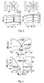
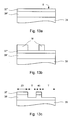
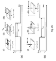
- a ferromagnetic element 1 of a magnetoresistive device in accordance with the present invention is shown.
- the ferromagnetic element 1 is assumed to have homogenously distributed magnetization, although this need not necessarily be the case.
- the ferromagnetic element 1 exhibits magnetic anisotropy defining a magnetic easy axis 2. Magnetic anisotropy may arise as a result of, inter alia , the shape of the element and/or crystal structure.
- the element 1 may be elongate and so the magnetic easy axis 2 may be aligned along a longitudinal axis.
- Magnetisation 4 of the element 1 is aligned along a magnetic easy axis 2.
- An external magnetic field 5 may optionally be applied to support precessional switching and, depending on orientation, to stabilize re-orientation of the magnetisation 3.
- the external magnetic field 5 may be applied globally to an array of ferromagnetic elements (of which the ferromagnetic element 1 is one).
- the external magnetic field 5 may be fixed along the hard axis to facilitate or assist the precessional switching, for example using a permanent magnet.
- the external magnetic field 5 is aligned anti-parallel to the initial magnetization along the easy axis 2 to stabilize re-orientation of the magnetisation 3.
- the external magnetic field 5 need not be aligned along the easy axis 2 and may be orientated at other angles including a hard axis which, for the arrangement shown in Figure 1 , is arranged perpendicular to the easy axis 2.
- the external magnetic field 5 may be variable and may be generated by passing a current through a conductive track (not shown).
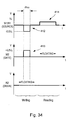
- an electric field pulse 7 may be applied, for example perpendicularly to the plane of the layer, to change magnetic anisotropy in the ferromagnetic element 1 temporarily and trigger precessional reorientation of the magnetization 3.
- the magnetization 3 shown as M
- the direction of the effective magnetic field 6 here designated as parallel to positive x-direction.
- more than one gate may be used.
- An electric field pulse 7 is then applied, which causes magnetic anisotropy to change and, thus, the magnetization 3 to be rotated and to begin precessing around the modified effective field.
- the anisotropy field 2 changes causing the effective magnetic field 6 to rotate, i.e. B ⁇ eff + V 0 ⁇ B ⁇ eff V C , and the magnetization 3 starts damped precession around the axis of effective magnetic field 6, i.e. around B eff ( V C ).
- the electric field 7 can be switched off.
- the magnetisation 3 then begins to stabilize (anti-parallel) along the easy axis 2.
- Magnetisation reversal may be understood by considering orientation-dependent energy of magnetization 3.
- the easy axis 2 along the x-axis corresponds to two energy minima divided by a potential barrier.
- the height of the barrier corresponds to the energy increase if the magnetization 3 is aligned along the hard axis.
- Magnetization reversal i.e. reorientation of magnetization by 180°
- TMR tunnelling magnetoresistance
- GMR gigantic magnetoresistance
- other similar types of read device where the relative orientation between the switched layer and a fixed reference layer determine the resistance of the device.
- the gate voltage pulse 7 results in a new easy axis which is rotated from the original easy axis 4 by more than 45° and up to 90°, then magnetization reversal can be achieved without using an assist magnetic field.
- Rotation of easy axis can also be achieved by changing the carrier density in a strained configuration.
- magnetic anisotropy variation can behave in an opposite way.
- magnetic anisotropy in a location in which the element is compressively strained, magnetic anisotropy may be orientated perpendicularly to the plane and in a location in which the element is in tensile strain, the magnetic anisotropy is orientated in plane
- magnetisation reversal is not necessary, in other words magnetisation need not be re-orientated by 180°.
- magnetization reorientation of 90° can be achieved in an element exhibiting cubic magnetic anisotropy, if the easy axis rotates by an angle less than or equal to 22.5° with a longer pulse length (e.g. a half precession pulse) or at larger angles up to 90° for a shorter pulse lengths (e.g. a quarter precession pulse). This can occur in such as we have observed in Ga 1-x Mn x As having very small strain variations resulting from changes in lattice constant of the order of ⁇ 0.01%.
- anisotropic magnetoresistance effects such as anisotropic magnetoresistance (AMR), tunnelling anisotropic magnetoresistance (TAMR) or Coulomb blockade anisotropic magnetoresistance (CBAMR) can be used to read out the magnetization orientation.
- AMR anisotropic magnetoresistance
- TAMR tunnelling anisotropic magnetoresistance
- CBAMR Coulomb blockade anisotropic magnetoresistance
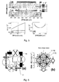
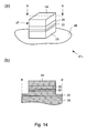
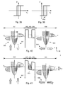
- Figures 2a and 2b illustrate a device 8 in which magnetocrystalline anisotropies are tuned and controlled using strain relaxation arising from lithographically-defined trenches 9.
- the magnetocrystalline anisotropies are induced by spin-orbit coupling.
- a van der Pauw device 10 is defined in the wafer 11 adjacent to the device 8.
- the device 8 is in the form of a Hall bar having a channel 11 which is 'L'-shaped in plan view and which includes first and second arms 11 1 , 11 2 orthogonally aligned along the [110] and [1 1 0] directions.
- the arms have a (transverse) width, w, of 1 ⁇ m and a (longitudinal) length, 1, of 20 ⁇ m.
- the device 8 is formed in a wafer having a layer structure 12 comprising a Ga 0.95 Mn 0.05 As epitaxially-grown layer 13 (or "epilayer) having a thickness of 25 nm grown along the [001] crystal axis on a GaAs substrate 14.
- the channel 11 is defined using electron beam lithography and reactive ion-beam etching.
- the trenches 9 have a (transverse) width, W, of 200 nm and a depth, d, of 70 nm.
- FIG. 3a to 3d electrical characteristics for another device (not shown) having an identical configuration to the device 8 and for the device 8 are shown.
- the other device (not shown) and the device 8 differ in the dimensions of the Hall bars.
- the arms (not shown) are 4 ⁇ m wide and 80 ⁇ m long.
- the arms 11 1 , 11 2 are 1 ⁇ m wide and 20 ⁇ m long.
- These devices 8 exhibit in-plane magnetocrystalline anisotropy and have a saturation magnetisation, M s , of about 50 mT. This arises due to the effect of strain relaxation rather than shape anisotropy.
- shape anisotropy fields for the devices 8 are less than 1 mT, which is one order of magnitude lower than the magnetocrystalline anisotropy fields.
- the easy axes are not defined by shape anisotropy, but rather than magnetocrystalline anisotropy.
- a Curie temperature (T c ) of 100 °K is estimated using Arrot plots of anomalous Hall data.
- a hole density of 5 ⁇ 10 20 cm -3 is estimated from high-field Hall measurements.
- compressive strain in the Ga 0.95 Mn 0.05 As epilayer 13 grown on the GaAs substrate 15 produces a strong magnetocrystalline anisotropy which forces magnetization vector to align parallel with the plane of the magnetic epilayer 13.
- Magnetization orientations in the individual microbar devices 8 are locally monitored by measuring longitudinal and transverse components of the anisotropic magnetoresistance (AMR) for in-plane rotating magnetic field (not shown).
- AMR anisotropic magnetoresistance
- ⁇ L,T ⁇ L,T - ⁇ L,T where ⁇ L,T is the average over all angles.
- Figures 3c and 3d show magnetoresistance plots for external magnetic field sweeps in which a field angle, ⁇ , measured from the [1 1 0] axis, is constant.
- magnetoresistance is strongly dependent at the values of ⁇ and is attributed to magnetization rotations.
- the magnetoresistance becomes purely isotropic, i.e. the differences between resistances for different angles ⁇ become independent of the magnitude of the external field.
- This property and the much smaller magnitude of the isotropic magnetoresistance compared to the low-field anisotropic magnetoresistance enables the high-field measurements shown in Figures 3a and 3b to be used to determine a one-to-one correspondence between a change in the low-field resistance and a change in magnetization orientation.
- the 45° phase shift between the longitudinal and transverse AMR traces shown in Figures 3a and 3b can be used to determine a change in the magnetization angle if both resistance components are measured simultaneously.
- a magnetization angle 30° corresponds to an easy-axis, while 7° and 55° are significantly harder.
- 7° is an easy axes in the [1 1 0]-bar and 55° is an easy-axis in the [110]-bar.
- Table 1 below lists easy axes found in the other device (not shown) labelled ⁇ A', the device 8 labelled 'B' and in bulk material, i.e. in the van der Pauw device 10: Table 1 Sample Bulk A [1 1 0] A [110] B [1 1 0] B[110] Easy axis angle ⁇ 30° ⁇ 15° ⁇ 36° +7°, -8° +55°, -63°
- Bulk material has cubic anisotropy arising from the underlying zincblende structure, plus an additional uniaxial [1 1 0] anisotropy arising from being an (Ga,Mn)As epilayer 13. This results in two easy axes tilted by 15 ⁇ from the [100]and [010] cube edges towards the [1 1 0] direction.
- the easy axes are rotated inwardly from the angles occupied in the bulk material towards the arms 11 1 , 11 2 .
- the degree of rotation increases as the width of the arms 11 1 , 11 2 decreases.
- the local changes in the magnetocrystalline anisotropy may be understood in the following way.
- Ga 0.95 Mn 0.05 As epilayers 13 grown on GaAs substrate 15 are compressively strained in the (001) plane with the typical value of the strain parameter: f ⁇ a GaMnAs - a GaAs a GaAs where a GaAs and a GaMnAs are the lattice parameters of cubic, fully-relaxed GaAs and (Ga,Mn)As, respectively.
- f ⁇ a GaMnAs - a GaAs a GaAs where a GaAs and a GaMnAs are the lattice parameters of cubic, fully-relaxed GaAs and (Ga,Mn)As, respectively.
- the lattice can relax in a transverse direction and the corresponding extension can be roughly estimated as ft / w ⁇ 0.01, where t is the thickness of the (Ga,Mn)As film, in this case 25 nm, and w is the bar width.
- the strength of the lattice relaxation in the microbars can be obtained using numerical elastic theory simulations for the realistic sample geometry.
- GaAs values of the elastic constants are considered for the whole wafer including the Ga 0.95 Mn 0.05 As epilayer 13.
- Figure 5a shows the strain component along the growth-direction [001]-axis with respect to the lattice parameter of a fully relaxed cubic GaAs, namely: e 001 ⁇ a 001 - a GaAs / a GaAs
- Figure 5 illustrates growth-induced lattice matching strain. Because of in-plane compression of the (Ga,Mn)As lattice, the elastic medium reacts by expanding the lattice parameter in the growth direction, as compared to a GaAs , i.e. e [001] / f > 1.
- the lattice can relax only in a direction perpendicular to the microbar orientation.
- the corresponding strain component calculated again with respect to the GaAs, is plotted in Figure 5b over the entire cross-section of device 11 and in Figures 5c and 5d along various cross sections through the [001]-[110] plane. While in the centre of the bar the in-plane relaxation is relatively weak, i.e. the lattice parameter remains similar to that of the GaAs substrate 15, the lattice is strongly relaxed near the edges of the bar 11. Averaged over the entire cross-section of the (Ga,Mn)As bar, relative in-plane lattice relaxation is found to be several hundredths of a per cent, i.e.
- Figure 6a illustrates easy-axes orientations in the [1 1 0] - and [110]-bars of the other 'L'-shaped device 15 and the L'-shaped device 8. Arrows 16 indicate the direction and strength of the patterning induced lattice relaxation.
- Lattice deformations breaking the [1 1 0]-[110] symmetry of the microscopic magnetocrystalline energy profile are illustrated by the diamond-like unit cells extended along [110] axis for the [110]-bar (bottom diamond) and along the [110]axis for the [110]-bar (right diamond).
- the devices just described use the mutual strain relaxation induced by micro-patterning of stripes from GaMnAs with in-plane magnetic anisotropy grown under compressive strain.
- wires which are patterned from tensile strained GaMnAs with perpendicular magnetic anisotropy relax by reducing their lattice constant.
- micro-patterning weakens the perpendicular magnetic anisotropy compared to the tensile strained GaMnAs bulk layer.
- Ferromagnetic metals also exhibit a sensitive dependence of the magnetocrystalline anisotropy on local strain. Any distortion of the equilibrium lattice changes the local anisotropy. In ultrathin films, strain is induced by the growth on a surface. Therefore, similar to GaMnAs, ultrathin layers of cobalt (Co), or iron (Fe) epitaxially grown on a GaAs [001] substrate exhibit both cubic magnetic anisotropy of the bulk, as well as a uniaxial contribution stemming from the interface.
- Co cobalt
- Fe iron
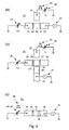
- First and second arrows 17, 18 indicate orientation of the easy axis for the first and second carrier densities respectively.
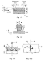
- magnetoresistance devices will be described in which application of an electric field pulse causes a change in charge carrier density in a ferromagnetic region which in turn causes a change in magnetic anisotropy which causes the magnetisation to begin precession.
- first and second magnetoresistive devices 21 1 , 21 2 are shown.
- the second devices 21 2 are variants of the first device 21 1 .
- Each device 21 1 , 21 2 includes a ferromagnetic region 22 (herein also referred to as a ferromagnetic "island”) which is under strain.
- the ferromagnetic region 22 comprises a ferromagnetic semiconductor, such as (Ga,Mn)As.
- a different ferromagnetic semiconductor may be used.
- the orientation of magnetisation of the ferromagnetic region 22 can be changed or helped to change by applying a short electric field pulse using a gate 23 capacitively coupled to the ferromagnetic region 22. Applying the electric field pulse causes a change in charge carrier density in the ferromagnetic region 22 which in turn causes a change in magnetic anisotropy which causes the magnetisation to begin precession.
- the ferromagnetic region 22 may be sufficiently small that it exhibits charging effects at a given operating temperature, such as at 4.2 °K.
- the ferromagnetic region 22 may have dimensions (layer thickness and lateral diameter) of the order of 1 or 10 nm. However, the ferromagnetic region 22 may be larger, for example having dimensions of the order of 100 nm, 1 ⁇ m or higher.
- the ferromagnetic island 22 is disposed between first and second leads 24, 25, and is weakly coupled to the leads 24, 25 by respective tunnel barriers 26, 27. In some embodiments, there may be more than one island of ferromagnetic material, for example arranged in chain.
- Reorientation of magnetisation is triggered using a pulse generator 28 which applies a voltage pulse 29 to the gate 23.
- Direction of orientation can be measured in different ways.
- orientation of magnetisation can be determined by measuring tunnelling anisotropic magnetoresistance (TAMR) using voltage source 30 and current detector 31. If the first and/or second lead 24, 25 is ferromagnetic, then the orientation of magnetisation can be determined by measuring tunnelling magnetoresistance (TMR) using voltage source 30 and current detector 31. In either case, the measurement involves applying a voltage so as to drive a current and measuring current.
- TAMR tunnelling anisotropic magnetoresistance
- TMR tunnelling magnetoresistance
- orientation of magnetisation can be determined using by measuring TMR using the voltage source 30 and the current detector 31. However, the bias is applied across and current is measured between the first lead 24 and a third lead 32 which is connected to a pinned ferromagnetic region 33 which is separated from the ferromagnetic island 22 by a tunnel barrier 34. It will be appreciated that a different measurement configuration can be used.
- the first device 21 1 is shown in more detail.
- the first device 21 1 has an elongate conductive channel 36 with the gate 23 arranged to the side of the channel 36, i.e. in a side gate configuration.
- the channel 36 and side gate 23 are formed in a patterned layer 37 of (Ga,Mn)As by trench-isolation.
- a layer 38 of AlAs electrically isolates the channel 36 and the side gate 23 from a GaAs substrate 39.
- the channel 36 includes a constriction 40 disposed between wider portions which provide the leads 24, 25 to the constriction 40.
- the (Ga,Mn)As layer 37 comprises 2% Mn, i.e. Ga 0.98 Mn 0.02 As, and has a thickness of 5 nm, although the effective thickness may be about 3 nm due to surface oxidation.
- the constriction 40 is 30 nm wide and 30 nm long.
- the channel 36 is 2 ⁇ m wide.
- the channel 36 and the gate 23 are separated by about 30 nm.
- potential fluctuations arising from disorder create at least one conductive island 22 and at least a pair of tunnel barriers 26, 27 which weakly couple the island 22 to leads 24, 25 and/or adjacent islands 22.
- Figure 10a is a greyscale plot of channel conductance against gate voltage and in-plane parallel-to-current magnetic field.
- a dashed line 41 highlights critical reorientation field, B C , which depends on gate bias.
- an effective disk diameter of about 10 nm can be estimated using the experimentally-found value of charging energy.
- about 40 Manganese acceptors are present on the island 22.
- About sixteen Coulomb oscillations are observed if V G is varied from -1V to +1V corresponding to a reduction of about 40% in carrier density.
- the second device 21 2 is a variant of the first device 21 1 .
- the devices 21 2 may be formed growing a layer of AlAs 38' on a GaAs substrate 39 followed by a layer of (Ga,Mn)As (not shown), patterning the (Ga,Mn)As to form a underlying electrode structure 42 comprising the pinned layer 32 and the third electrode 33 as a single piece, then growing a further layer of AlAs 43 and a further layer of (Ga,Mn)As over the patterned substrate and patterning the further layer of (Ga,Mn)As to form the channel 37' and gate 23.
- An overlying electrode structure can be used instead of an underlying electrode structure.
- the AlAs layer and (Ga,Mn)As layer forming the electrode may be grown after the channel and gate has been formed and patterned to form the electrode structure comprising the pinned layer and the third electrode.
- a thin gate dielectric, such as Si x N y , and a ferromagnetic material, such as Co may be deposited and patterned using lift-off or dry etching.
- the devices 21 1 , 21 2 can exhibit four states M 1 , M 2 , M 3 , M 4 .
- the devices 21 1 , 21 2 can exhibit fewer states, for example just two states which may be anti-parallel, or more states, for example six states by taking advantage of in-plane bi-axial anisotropy and perpendicular uni-axial anisotropy.
- the devices 21 1 , 21 2 can exhibit, for example, four states M 1 , M 2 , M 3 , M 4 , depending on whether, for example, the source and/or drain region is ferromagnetic, all states may be distinguishable or, alternatively, some states may be indistinguishable.
- plot of magnetisation 44 shown in Figure 12 does not represent energy of magnetisation, but merely represents different states. In some embodiments, they may represent angle dependencies 0°, 90°, 180°, 270°.
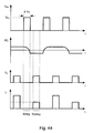
- a voltage pulse 29 is applied to the gate 23.
- the pulse 29 has duration, t 180 , which is half the period of precession, t precess .
- t precess is about1 ns.
- the value of t precess may lie typically in the range of 100 ps to 10 ns (for B a 100 mT to 1 mT).
- is of the order of 1 or 10 V.
- an external magnetic field may be applied to help stabilise magnetisation or to facilitate precession.
- the external magnetic field may be provided by a permanent magnet (not shown) or by a conductive track (not shown) and preferably has a magnitude which is about the same order but smaller than the anisotropy field, for example of the order of 1 to 100 mT.
- an external magnetic field and/or spin transfer torque current may be used to write a particular state (as opposed to toggle between states) by orientating the magnetisation 44 in a particular direction.
- this is referred to as "direct writing”.
- re-orientation of the magnetisation may achieved by applying the electric field pulse and simultaneously or shortly afterwards applying a spin transfer torque (STT) current pulse.
- STT spin transfer torque
- a bias pulse 45 is applied between the source 24 and drain 25 of the device 21 1 , 21 2 and the current 31, i, is measured.
- the magnitude of the current depends on the tunnelling anisotropic magnetoresistance (TAMR) and/or the tunnelling magnetoresistance (TMR) of the device which in turn depends on the orientation of magnetisation 44 of the ferromagnetic region 22 which represents '0' and '1' states.
- TAMR tunnelling anisotropic magnetoresistance
- TMR tunnelling magnetoresistance
- orientation of more than two states can be determined by measuring anisotropic magnetoresistance effects such as AMR, TAMR and CBAMR or by measuring a transverse Hall voltage between lead 32 and a reference (e.g. ground) arising from the anomalous Hall effect for states along a perpendicular-to plane magnetic easy axis.
- anisotropic magnetoresistance effects such as AMR, TAMR and CBAMR
- a transverse Hall voltage between lead 32 and a reference e.g. ground
- the device 21 1 is fabricated from an ultra-thin (5nm) Ga 0.98 Mn 0.02 As epilayer 37" grown along the [001] crystal axis on a AlAs 38" buffer layer on a GaAs substrate 39 by low-temperature molecular beam epitaxy (LT-MBE) and reference is made to " High-quality GaMnAs films grown with arsenic dimers" by R. P. Campion, K. W. Edmonds, L. X. Zhao, K. Y. Wang, C. T. Foxon, B. L. Gallagher and C. R. Staddon, Journal of Crystal Growth, volume 247, p 42 (2003 ).
- LT-MBE low-temperature molecular beam epitaxy
- Hall bar 14 is defined using electron-beam lithography using a poly-methyl-methacrylate (PMMA) resist developed using ultrasound in a methyl isobutyl ketone/isopropanol 1:3 mixture at 25 °C.
- PMMA poly-methyl-methacrylate
- Thermally-evaporated, high-electron-contrast Cr/Au registration marks (not shown) having thicknesses of 20 nm and 60 nm respectively are patterned by lift-off using 1 ⁇ m-thick resist (not shown) and ⁇ 250 nm electron-beam diameter. A 30 s dip in 10% HCl solution is used prior to evaporation to assist adhesion of metal without unduly damaging the GaMnAs.
- a ⁇ 200 nm-thick layer of resist (not shown) is applied to the surface S of the Ga 0.98 Mn 0.02 As epilayer 37.
- the finest features are defined using an electron-beam (not shown) having a ⁇ 15 nm beam diameter and ⁇ 5 pA current, with on-chip focusing at adjacent registration marks.
- Less-critical areas are defined in the same resist by a ⁇ 250 nm beam at ⁇ 1 nA.
- the high-resolution regions are arranged to be as small as possible to minimise write time and pattern drift.
- the resist is developed to leave a patterned resist layer M as an etch mask.
- RIE reactive-ion etching
- devices are arranged in a Hall-bar layout aligned along [110] direction, with a 2 ⁇ m-wide channel and three pairs of Hall sensor terminals of 500 nm width at 10 ⁇ m intervals either side of the constriction.
- Hall-bar layout aligned along [110] direction, with a 2 ⁇ m-wide channel and three pairs of Hall sensor terminals of 500 nm width at 10 ⁇ m intervals either side of the constriction.
- Hall sensor terminals 500 nm width at 10 ⁇ m intervals either side of the constriction.
- other arrangements can be used.
- the fabrication process hereinbefore described is modified to fabricate the second devices 21 2 .
- a different initial layer structure is used having a thicker GaMnAs layer, e.g. 25 nm thick.
- the layer structure is patterned using electron beam lithography and RIE to form an underlying electrode structure 44 ( Figure 11a ).
- another AlAs layer (having a thickness of 3nm) and a layer of GaMnAs are grown by LT-MBE as described above.
- the structure is patterned to define the channel in a similar way to the first device 21 1 .
- the underlying electrode structure 44 ( Figure 11a ) may be patterned using ion-beam milling immediately after growth of the initial layer structure, then the additional layers grown without breaking vacuum.
- the third device 21 3 is a two-terminal device having a ferromagnetic region 22 disposed between first and second leads 24, 25 and is weakly coupled to one of the leads 24 by a tunnel barrier 26 and to the other lead 25 by a tunable barrier 35 provided by a region of depletion formed by the semiconducting ferromagnetic region 22 and the lead 25.
- the ferromagnetic region 22 comprises a p-type semiconductor, e.g. Ga(Mn,As) and the lead 25 comprises an n-type semiconductor, e.g. Si doped GaAs, and so the tunable barrier 35 is a reversed-biases p-n junction.
- the lead may be metallic and so the tunable barrier 35 may be a Schottky barrier.
- the device 21 3 comprises a pillar 47 upstanding from a substrate 48.
- the pillar 47 includes a layer 25 of GaAs doped to a concentration of the order of 1-10 ⁇ 10 18 cm -3 and having an (unetched) thickness of 200 nm, a layer 22 of p-type Ga 0.98 Mn 0.02 As having a thickness of about 5 nm, a layer 26 of AlAs having a thickness of 25 nm and a layer of Au having a thickness of about 10 nm.
- the device is fabricated from a layer structure (not shown) grown on an GaAs substrate (not shown) comprising, in order a 200 nm thick layer of n-type GaAs (not shown), a 5 nm thick layer of Ga 0.98 Mn 0.02 As and a 25 nm thick layer of AlAs.
- the Ga 0.98 Mn 0.02 As is grown by low-temperature molecular beam epitaxy (LT-MBE).
- Electron beam lithography and thermal evaporation are used to define a pad of gold (Au) having a thickness of the order of 10 nm on the surface of the layer structure (not shown) and SiCl 4 /Ar RIE is used to define the pillar 47.
- the pillar may be planarised using, for example polyimide, and depositing a gold contact pad.
- a non-magnetic ohmic contact is used to contact the substrate.
- the third device 21 3 can exhibit can exhibit four states M 1 , M 2 , M 3 , M 4 .
- the third device 21 3 differs in that the polarity of a voltage pulse 29 determines whether it is a write or read pulse.
- a negative voltage pulse 29 is applied to the lead 24 adjacent to the fixed tunnel barrier relative to the other lead 25 so as to reverse bias the p-n junction 35 and increase the width of the depletion region to increase depletion and vary the carrier density or carrier density distribution in the ferromagnetic region 22 and, thus, induce precession.
- the duration of the pulse can be use to switch between two states or between more than two states, in other words using t 90 and t 180 pulses.
- a positive bias pulse 30 is applied to the lead 24 adjacent to the fixed tunnel barrier relative to the other lead 25 and the magnetization orientation depending current 46, i, is measured.
- a magnetoresistive device 51 will now be described in which application of an electric field pulse causes a shift in maximal carrier concentration in an inhomogeneously strained ferromagnetic semiconductor which in turn causes a change in magnetic anisotropy and so initiates precession of magnetisation.
- the device 51 comprises a Hall bar 52 which is generally elongate having width, w, of about 1 ⁇ m and a length, 1, of about 20 ⁇ m.
- the Hall bar 52 has first and second end leads 53, 54 and first, second, third and fourth side leads 55, 56, 57, 58 arranged in pairs on opposite sides of the bar 52.
- the Hall bar 52 is sandwiched between underlying and overlying electrodes 59, 60, hereinafter referred to as "bottom” and “top” electrodes respectively.
- a pulse generator 61 is used to apply a voltage pulse 62 between the top and bottom electrodes 59, 60.
- a current source 63 is used to apply a read current, i read , through the Hall bar 52 between the first and second end leads 53, 54.
- First and second voltage meters 64, 65 measure bias between the first and second leads 55, 56 and between the second and fourth side leads 56, 58 so as to determine longitudinal and transverse anisotropic magnetoresistance (AMR) respectively.
- the bias measured between the second and third side leads 56, 57 can also be used to measure the anomalous Hall effect (AHE) resistance.
- AHE anomalous Hall effect
- the Hall bar 52 is formed on an indium gallium arsenide (In 0.05 Ga 0.95 As) substrate 66 which serves as the bottom electrode 59.
- the Hall bar 52 includes a base barrier layer 67 formed of AlAs overlying the InGaAs substrate 66, an inhomogeneously-strained ferromagnetic layer 68 formed of graded InGaMnAs and a top barrier layer 69 formed of AlAs.
- the top gate electrode 60 is formed of Al.
- the lattice constant within the ferromagnetic layer 68 is controllably varied so as to produce inhomogeneous strain within the layer 68.
- the lattice constant of In 0.03 Ga 0.97 As is larger than the lattice constant for Ga 0.95 Mn 0.05 As so that the subsequent Ga 0.95 Mn 0.05 As grown on In 0.03 Ga 0.97 As is tensile strained.
- Indium is introduced again to form InGaMnAs.
- the Indium concentration is increased until the lattice constant of InGaMnAs becomes larger than the lattice constant of the InGaAs substrate to achieve compressive strain.
- a layer 68 1 ' of Ga 1-x Mn x As is epitaxially grown under tensile strain on top of the AlAs layer 67' which in turn is grown on the In y Ga 1-y As substrate 66'.
- the wider lattice constant of the In y Ga 1-y As substrate 66' is transmitted to the Ga 1-x Mn x As layer 68 1 ' which introduces tensile strain.
- indium is introduced to increase further the lattice constant by thereby forming a quaternary alloy, InGaMnAs.
- the indium concentration [In] increases with increasing distance, d, from the base 71 of the layer 68 1 .
- strain profiles can be used. For example, instead of the strain within the ferromagnetic layer 68 varying from being tensile closer to the substrate to being compressive further away from the substrate, it may change from being compressive to tensile.
- This can be achieved by fabricating the device from a wafer having a gallium arsenide (GaAs) substrate instead of In y Ga 1-y As substrate and introducing phosphorous (P) instead of indium (In) to form a graded layer of gallium manganese phosphide arsenide (Ga 1-x Mn x P z As 1-z ). The lattice constant is reduced as the phosphorous concentration is increased.
- GaAs gallium arsenide
- P phosphorous
- In indium
- strain can also be varied by changing the shape of ferromagnetic layer 68.
- the width of the ferromagnetic layer 68 may be made narrower at the base 71 of the layer 68 having a width w 1 and made wider further away from the base 71 having a width w 2 > w 1 .
- the ferromagnetic layer 68 may be homogenously doped.
- an electric field 72 is generated which shifts charge carriers 73 (here only holes, the majority carriers, are illustrated) and alters charge carrier concentration in a lower, tensile-strained region 74 and in an upper, compressively-strained region 75.
- the pulse draws carriers 73 from the lower, tensile-strained region 74 into the upper, compressively-strained region 75 so as to increase charge carrier density in the upper, compressively-strained region 75.
- Table 2 below identifies orientation of magnetic anisotropy with strain and carrier concentration: Table 2 Tensile Strain Compressive strain High carrier concentration Out of plane In plane Low carrier concentration In plane Out of plane
- Magnetic anisotropy 76 of the magnetic layer 68 changes from being orientated in a first position 77 1 perpendicular to the plane of the layer 68 (i.e. along axis 78) to a second orientation 77 2 orientated along the plane of the layer 68 (e.g. along axis 79).
- the effective anisotropy field B A rotates by 90°. This causes the magnetisation 80 to begin precession and to be re-orientated by 90 degree for a ⁇ /2-pulse.
- Writing and reading cycles are similar to those shown in Figure 12 described earlier. However, during a read cycle, instead of applying a source-drain bias and measuring current, a current is driven through the device and the potential difference developed between leads 55, 56, 57, 58 is measured.
- the device 51 is fabricated using similar techniques to those described earlier to fabricate the first device 21 1 .
- a layer structure is grown in a similar way to that described earlier and is patterned using electron-beam lithography and RIE.
- a fourth magnetoresistive device 81 will now be described in which application of a strain pulse causes a change in magnetic anisotropy and so starts precession of magnetisation.
- the device 81 comprises a stacked layer structure 82 mounted on a piezoelectric layer 83 having first and second contact leads 84, 85.
- First and second contacts 86, 87 are used to provide electrical contacts to the layer structure 82.
- the stacked layer structure 82 has a width, W, of about 1 ⁇ m and a length, L, of about 1 ⁇ m.
- a pulse generator 88 is used to apply a voltage pulse 89 between the piezoelectric contact leads 86, 87.
- a voltage source 90 is used to apply a bias between the contact 86, 87 and a current meter 91 is used to measure the current flowing through the stacked layer structure 82.
- the stacked layer structure 82 is formed on a gallium arsenide (GaAs) substrate 92 which mounted by glue 93 to the piezoelectric stressor 83.
- the piezoelectric stressor is formed from lead-zirconate-titanate (PZT).
- the stacked layer structure 82 includes a bottom contact layer 94 comprising (non-ferromagnetic) n + -GaAs, a ferromagnetic layer 95 having a relatively low coercivity (i.e. a "free” layer) comprising Ga 0.98 Mn 0.02 As and having a thickness of 5 nm, a tunnel barrier layer 96 comprising aluminium arsenide (AlAs) having a thickness of 25 nm, a ferromagnetic layer 97 having a relatively high coercivity (i.e. a "pinned” layer) comprising Ga 0.98 Mn 0.02 As having a thickness of 50 nm and a top contact layer 98 comprising (non-ferromagnetic) gold.
- a bottom contact layer 94 comprising (non-ferromagnetic) n + -GaAs
- a ferromagnetic layer 95 having a relatively low coercivity i.e. a "free” layer
- AlAs
- the piezoelectric stressor 83 may be integrally formed with the substrate 92.
- GaAs is piezoelectric along the [110] axis.
- the ferromagnetic layer(s) of the fourth device 81 need not be a semiconductor but may be metallic and may comprise a material, such as ferromagnetic metals like Fe, Ni, Co or metal alloys FePt, CoPt, CoPd or another suitable transition metal/noble metal alloy.
- a stacked layer structure need not be used. Instead, an "in-plane" transport structure, e.g. similar to that shown in Figure 9 , can be used.
- the structure shown in Figure 9 may be mounted on a piezoelectric stressor 83.
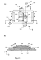
- the device 101 comprises a cruciform mesa 102 which defines a channel 103 of ferromagnetic material, which in this case is a delta-doped layer of Ga 0.98 Mn 0.02 As embedded in layer 104 of GaAs, and which is supported by substrate 105.
- First, second, third and fourth contact 106, 107, 108, 109 provide contacts to the distal ends of the channel 103 and a surface top gate 110 is used to control magnetic anisotropy.
- the substrate 104 is mounted on a piezoelectric layer 111 having first and second contacts 112, 113 which are used to generate an electric field within the piezoelectric layer 111 for pre-stressing the ferromagnetic channel 103.
- the arms of the channel 103 each have a width of about 2 ⁇ m and a length of about 20 ⁇ m.
- a first pulse generator 114 is used to apply a voltage pulse 115 between the piezoelectric contact leads 112, 113 for pre-stressing the channel 103.
- a second pulse generator 116 is used to apply a voltage pulse 117 to the surface gate 110 for inducing precession of magnetic anisotropy.
- a voltage source 118 is used to apply a bias 119 between the first and second contact 106, 107 and a current meter 120 is used to measure the current 121 flowing between the third and fourth contacts 108, 109.
- the substrate 104 is mounted to the piezoelectric layer 111 by a layer of glue 122.
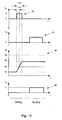
- writing and reading of data to the devices is based on treating the device as if it had only two states and, thus, store only one bit of information per device.
- six remnant magnetisation orientations can be accessed using two types of combination of pulses and inverted pulses so as to encode more than 2 bits (i.e. ln 6/ln 2 ⁇ 2.6 corresponding to 6 different states).
- the ferromagnetic layers 22, 68, 95, 103 exhibit six remnant magnetisation orientations 131, 132, 133, 134, 135, 136.
- precessional switching triggered by fast gate-voltage pulses with different pulse lengths rotate the magnetization vector between the four remnant states 131, 132, 133, 134 along the two biaxial easy axes within the layer plane.
- an adjacent magnetisation orientation 131, 132, 133, 134 can be accessed from another of the first, second, third and fourth magnetisation orientations 131, 132, 133, 134 using a gate pulse 29, 62, 91 which effects a 90° rotation.
- This type of pulse is herein referred to as a "p 90° pulse” or "t 90 pulse”.
- an adjacent magnetisation orientation 131, 132, 133, 134 can be accessed from another of the first, second, third and fourth magnetisation orientations 131, 132, 133, 134 using a gate pulse (not shown) which effects a 270° rotation.
- a gate pulse not shown
- p 270° pulse or "t 270 pulse”.
- the first, second, third and fourth magnetisation orientations 131, 132, 133, 134 can also be accessed from a co-linear orientations 131, 132, 133, 134 using a gate pulse 138 which effects a 180° rotation, hereinafter referred to as a "p 180° pulse” or "t 180 pulse”.
- a gate pulse 138 which effects a 180° rotation
- the first magnetisation orientation 131 can be access the third magnetisation orientation 133 using the p 180° pulse 138.
- Changing between biaxial-in-plane and uniaxial-perpendicular-to-plane anisotropy regimes is achieved by "adiabatic" magnetization reorientation which exploits dissipative damping.
- the magnetization vector M starts precessing around a modified anisotropy field B A (V C ) and dissipative damping causes the magnetization vector to spiral towards modified anisotropy field B A (V C ).
- the magnetization vector M eventually aligns (within thermal fluctuations) along one of the easy axes corresponding to the modified anisotropy.
- the fifth and sixth magnetisation orientations 135, 136 can be accessed by using a gate pulse 141 which effects a 180° rotation.
- the pulse 141 is inverted with respect to the p 180° pulse 108 and is hereinafter referred to as an "inverted p 180° pulse.
- Figures 25b shows that an inverted pulse triggers a 180° reversal in the perpendicular-to-plane anisotropy regime.
- An AHE measurement can distinguish between two uniaxial magnetization states along perpendicular-to-the-plane orientation and measurements of transverse and longitudinal AMR can unambiguously distinguish the 4 biaxial magnetization states within the plane.
- magnetic anisotropy is varied electrically using a gate or using the piezoelectric effect.
- magnetic anisotropy can also be controlled optically, as will now be described in more detail.
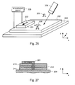
- a ferromagnetic element 201 is coupled to an optically-controlled stressor 202 supported on a substrate 203.
- a photon source 204 typically in the form of a laser
- a pulse of light 205 can be used to generate a phonon pulse 206 in the stressor 202.
- the phonon pulse 206 causes magnetisation 207 of the ferromagnetic element 201 to switch between first and second orientations, in a similar way to that described earlier.
- Additional structure such as a pinned ferromagnetic element (not shown) and a tunnel barrier layer separating the pinned ferromagnetic element and the ferromagnetic element 201 may be provided, to measure the state of the element 201 using tunnelling magnetoresistance measurement (TMR).
- TMR tunnelling magnetoresistance measurement
- a measurement circuit 208 for example, comprising a voltage source and a current meter in series, can be used to measure magnetoresistance using a TMR measurement or a tunnelling anisotropic magnetoresistance (TAMR) measurement.
- TAMR tunnelling anisotropic magnetoresistance
- the ferromagnetic element 201 can be formed from a thin layer (e.g. about or less than 1 nm) of semiconducting material, such as GaMnAs, or from a metallic ferromagnetic material, such as Fe, Ni or Co, or alloys or multilayers, such as FePt, CoPt or CoPd.
- the ferromagnetic element 201 can have lateral dimensions (i.e. x- and y-directions) of the order of a few nanometres.
- the stressor 202 includes a quantum well heterostructure comprising a lower GaAs layer 211, an InGaAs layer 212 and an upper GaAs layer 213 formed on a GaAs substrate 203.
- concentration of In (and or Al, if used) in the InGaAs layer 212 can be chosen according the wavelength of light to be absorbed and the recombination required to generate phonon(s).
- the stressor 202 may have lateral dimensions of the order of a few nanometres or a few tens of nanometres.
- AlGaAs can be used instead of GaAs and InGaAlAs can be used instead of InGaAs.
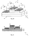
- a ferromagnetic element 221 is supported on one surface 222, e.g. front side, of a substrate 223 and a stressor 224 is coupled to the substrate 223 on another surface 225, e.g. reverse side.
- a photon source 226, e.g. laser e.g. laser
- a pulse of high intensity light 227 causes the stressor 224 to heat up and expand, thereby causing a stress pulse, i.e. phonon pulse, which is transmitted through the substrate to the ferromagnetic element 221.
- the phonon pulse causes magnetisation 228 of the ferromagnetic element 201 to switch between first and second orientations, in a similar way to that described earlier.
- Additional structure such as a pinned ferromagnetic element (not shown) and a tunnel barrier layer separating the pinned ferromagnetic element and the ferromagnetic element 221 may be provided, to measure the state of the element 221 using tunnelling magnetoresistance measurement (TMR).
- TMR tunnelling magnetoresistance measurement
- a measurement circuit 229 can be used to measure magnetoresistance using a TMR or TAMR measurement.
- the ferromagnetic element 221 can be the same as the element 201 ( Figure 26 ) described earlier.
- the stressor 224 may comprises a pad of aluminium or other metallic material.
- the substrate 223 may comprise, for example, glass, silicon or GaAs.
- the substrate 223 can be thinned to form a membrane, e.g. a few microns thick, in a region supporting the ferromagnetic element 221 and stressor 224.
- magnetic anisotropy in a ferromagnetic element can be controlled using a gate. If the ferromagnetic element is formed of a semiconducting material, then magnetic anisotropy can be varied by controlling carrier density. However, even if the ferromagnetic element is formed of a metallic material, then magnetic anisotropy can still be varied electrically, using a gate, as will now be explained in more detail.
- the (total) magnetic anisotropy is governed by a plurality of contributions including crystalline anisotropy which can depend on the Fermi energy, surface and interface anisotropy, shape anisotropy and lattice deformation magnetic anisotropy.
- the contribution due to surface and interface anisotropy can be large and can exceed the other contributions and so dominate the overall magnetic anisotropy.
- the magnetic anisotropy of cobalt and platinum multilayers become orientated perpendicular to the plane, if the thickness of the layer of cobalt is less than 1 nm. It then becomes larger than the shape anisotropy.
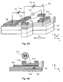
- a magnetoresistance device 301 is shown.
- the device 301 is formed on an insulating substrate 302 of silicon dioxide and comprises a conductive sheet 303 and an overlying ferromagnetic multilayer structure 304.
- a dielectric layer 305 overlies a first portion of a top 306 of the ferromagnetic multilayer structure 304.
- the dielectric layer 305 comprises a material having a large value of dielectric constant (compared to silicon dioxide), such as zirconium oxide (k ⁇ 12.5) or tantalum oxide (k ⁇ 11.6).
- a first electrode (“source”) 307 contacts the conductive sheet 303
- a second electrode (“drain”) 308 contacts a second portion of the top 306 of the ferromagnetic multilayer structure 304
- a third electrode (“gate”) 309 is arranged on a top 310 of the dielectric layer 305.
- the second electrode 308 may comprise a ferromagnetic material, such as cobalt, having a thickness of a few nanometres.
- drain 308 and gate 309 are configured in a side-by-side arrangement.
- other arrangements e.g. annular or interdigitated arrangements, may be used.
- a measurement circuit 311 may comprise first and second voltage sources 312, 313 for applying biases, V S , V G , to the source electrode 307 and gate electrode 309 respectively.
- Source-drain current, I DS can be measured by a current meter 314 arranged between the drain 308 and ground.
- the conductive sheet 303 comprises a layer 315 of tantalum (Ta) having a thickness of about 3 nm and an overlying layer 316 of platinum (Pt) having a thickness of about 3 nm.
- the layer of tantalum can help to form a smooth surface for the overlying platinum layer 316 and ferromagnetic layer structure 304.
- the ferromagnetic layer structure 304 comprises an ultrathin layer 317 of cobalt (Co) having a thickness of 0.4 nm and an overlying layer 318 of aluminium oxide (AlO x ) having a thickness of about 1 nm.
- Co cobalt
- AlO x aluminium oxide
- the ferromagnetic layer structure 304 is formed by d.c. sputtering a layer of cobalt followed by a layer of aluminium about 1 nm-thick and allowing the layer of aluminium to be oxidized in dry oxygen.
- the structure is annealed at a temperature of about 114°C for about 20 minutes in order to bring the anisotropy of the layer in the layer of cobalt close to a transition in magnetic anisotropy between being in-plane and perpendicular-to-plane (i.e. x-y plane) and, thus, magnetization.
- An overlying layer of platinum (not shown) having a thickness of about 3 nm can also be deposited over the layer of aluminium oxide and which can be patterned to provide the drain contact 308.
- An electric field e.g. applied by the gate electrode 309 and/or the source electrode 307, can be used to trigger a change in magnetic anisotropy.
- a set of writing and reading cycles for the device 301 is shown for toggling the device 301 between states.
- a positive voltage pulse 321 is applied to the gate electrode 309. Concurrently, the source electrode 307 is grounded and the drain electrode 308 is allowed to float.
- the pulse 321 has sufficient magnitude, e.g. to produce an electric field of the order 10 6 or 10 7 V/cm.
- the pulse 321 has a duration, t 180 , which is half of the precession period, t precss , which can be calculated using equation (6) earlier.
- the gate electrode 309 is grounded or allowed to float while a positive voltage pulse, V m , is applied to the source electrode 307 relative to the drain electrode 308 (which may be grounded).
- the source-drain current, I SD , 323 is measured and reflects the state of the device, i.e. direction magnetization, e.g. which may be in-plane or perpendicular to plane.
- the device 301 can operate at higher temperatures, e.g. up to or at room temperature, for example if the Currie temperature is greater than the operating temperature, e.g. room temperature, and if anisotropy density energy times the volume of the element (kxV) is greater than 50 k B T, where k B is Boltzmann's constant and T is operating temperature in Kelvin.
- Transition metals such as platinum (Pt), palladium (Pd) or iridium (Ir), as an alloyed interfacial layer or as thin, polarisable layer, e.g. one or two monolayers thick, can enhance interface and surface anisotropy and, thus, increase the operating temperature.
- a magnetoresistance device in accordance with the present invention for example device 21 1 ( Figure 8a ) or device 301 ( Figure 30 ) can serve as the basis of a memory element in a memory array 401.
- the memory array 401 is described based on the device 301 shown in Figure 30 .
- the memory array 401 includes an array of cells 402 each including a magnetoresistance device 403.
- the cells 402 can be selected and data written to or read from the cell 403 via first, second and third lines 404, 405, 406 driven by row and column decoders 407, 408.
- the device 403 has source, drain and gate electrodes 409, 410, 411.
- a negative voltage pulse 412 is applied the first line 404 and, concurrently, a positive voltage pulse 413 is applied to the third line 406 so as to select and write data to a selected cell 402.
- the second line 405 is allowed to float.
- each pulse 412, 413 is such that a pulse 412, 413 is insufficient to trigger a change in magnetic anisotropy by itself. However, together the pulses generate a larger field which is able to trigger the change. Thus, the magnitude of each pulse is about 0.5V A .
- the pulses 412, 413 each have a duration, t 180 , which is half of the precession period, t precss ,.
- a positive voltage pulse 414 is applied the first line 404, while the third line 406 (i.e. gate) is allowed to float and second line 405 (i.e. drain) is grounded. Current flow can be measured through the first and second lines 404, 405 and, thus, measure the state of the cell.
- an alternative memory cell 402' is shown.
- the cell 402' is similar to the cell 402 described earlier based on the device 301 shown in Figure 30 .
- the cell 402' includes a field effect transistor 420 and so can be addressed in a different manner.
- the cell 402' is formed on an insulating substrate 302'.
- the substrate 402' supports a gate electrode 421 isolated by a gate dielectric 422 from an overlying conductive channel 423.
- the gate electrode 421 comprises highly-doped, n-type silicon (n + - Si)
- the gate dielectric 422 comprises silicon dioxide
- the conductive channel 423 comprises, for example, undoped or lightly doped, p-type silicon (p - - Si).
- Highly-doped, n-type wells provide source and drain electrodes 424, 425 for the field effect transistor 420.
- the drain electrode 425 (or end of the channel) is connected to ground via a resistor 426.
- the conductive base layers 303' and ferromagnetic layer structure 304' are formed on the drain electrode 425 in the same way as described earlier. It will be appreciated that other semiconducting materials, including organic semiconducting materials, can be used.
- a first negative voltage pulse 427 is applied to the third line 406 and, concurrently, a second positive voltage pulse 428 is applied to the first line 404 so as to select and write data to a selected cell 402'.
- the second line 405 and, thus, the drain of the magnetoresistance device 308, is allowed to float.
- the magnitude of first voltage pulse 427 is about ⁇ V A ( ⁇ > 1 and such that the drain is at V A ) and has a duration of a duration, t 180 , which is half of the precession period, t precss ,.
- a positive voltage pulse 429 is applied the second line 405 (i.e. to magnetoresistance device drain).
- the first line 404 and, thus, the source 424 of the FET 420 is held low, e.g. at ground.
- the FET 420 is then turned on to allow conduction through the FET 420 and through the magnetoresistance device 403'.
- re-orientation of magnetization is triggered by a change in magnetic anisotropy and can be electrically controlled, for example, using a gate.
- re-orientation of magnetization can also be achieved through exchange coupling and which can also be electrically controlled, for example, using a gate. This will now be described in more detail.
- Exchange coupling is the interaction between localized magnetic moments of atoms, mediated by spin of the conduction electrons. This effect is employed in TMR and GMR devices to couple adjacent ferromagnetic (FM) layers in a ferro- or antiferromagnetic arrangement.
- exchange coupling can be used to pin a ferromagnetic layer with respect to a free layer as in a synthetic antiferromagnet (SAF).
- IEC interlayer exchange coupling
- FIG. 40 a band diagram of a device which uses exchange coupling to switch magnetization in response to an applied bias is shown.
- the device includes a first ferromagnetic electrode 501, a first tunnel barrier layer 502, a quantum well layer 503, a second tunnel barrier 504 and a second ferromagnetic electrode 505.
- the tunnel barrier layers 502, 504 and quantum well layer 503 define a double barrier structure having a quantum well which includes one or more resonant state(s) 506.
- the first ferromagnetic electrode 501 has an easy axis along an x - direction with fixed magnetization orientation 507.
- the second ferromagnetic electrode 505 has an easy axis along y-direction with fixed magnetization orientation 508. Densities of states 509, 510 for the ferromagnetic electrodes 501, 505 are shown schematically. At zero bias, the double barrier is off-resonance and exchange interaction is suppressed.
- the first ferromagnetic electrode 501 may have, for example, in-plane magnetic anisotropy with pinned magnetization orientation, e.g. using a synthetic antiferromagnet (not shown).
- the second ferromagnetic electrode 505 may have, for example, perpendicular-to-plane magnetic anisotropy due to, for example, choice of layer thickness and/or surface/interface anisotropies.
- applying a bias voltage between the first and second ferromagnetic electrodes 501, 505 shifts the energies of the resonant states with respect to the Fermi energies of the ferromagnetic electrodes 501, 505 so that a state 506 is brought into resonance and the transmission probability between electrons with an energy ⁇ F FM1 becomes very high so that the interlayer interaction becomes large.
- exchange torque along z-orientation acts on the magnetization 508 of the second ferromagnetic electrode 505.
- This exchange torque may be used to cause precession of the magnetization 508 or to support precession in addition to an external magnetic field which is oriented along the first magnetization 507 and perpendicular to the second magnetization 508.
- An arrangement which uses bias-controlled exchange torque can have the advantage of allowing magnetization to be switched using a small applied voltage, for example of about a few volts.
- the device comprises a stacked structure which includes a first ferromagnetic layer 601, a first tunnel barrier layer 602, a quantum well layer 603, a second tunnel barrier 604, a second ferromagnetic layer 605, a third barrier 606 and third ferromagnetic layer 607.
- the first and third ferromagnetic layers 601, 607 are pinned with in-plane and perpendicular-to-plane anisotropy, respectively.
- the stacked structure is arranged on an insulating substrate 608 and is stepped so as to allow contacts 609, 610, 611 to each of the ferromagnetic layers 601, 605, 607.
- the ferromagnetic layers 601, 605, 607 may comprise cobalt.
- the second ferromagnetic layer 605 can be made thin, e.g. ⁇ 1nm, and may have an overlying layer of platinum, as described earlier.
- the tunnel barrier layers and the quantum well layer may be formed from AlGaAs and GaAs respectively or other similar systems.
- a circuit 612 for controlling a measuring the device includes a first voltage source 613 for applying a bias voltage between the first and second ferromagnetic layers 601, 605 and a second voltage source 614 for applying a measurement voltage between the second and third ferromagnetic layers 605, 607.
- a current meter 615 is used to measure current.
- Magnetizations 616, 617, 618 of the ferromagnetic layers 601, 605, 607 are shown.
- the two possible equilibrium orientations of the magnetization 617 of the second magnetization layer 605 can be detected by a resistance TMR measurement between the second and third ferromagnetic layers 605, 607.
- the read-out involves a TMR measurement between the second and third ferromagnetic layers 605, 607.
- FIG. 45 and 46 another device is shown which uses bias-controlled exchange torque to switch magnetization.
- the device is simpler to fabricate than the device shown in Figures 42 and 43 in that it has fewer layers in particular the third ferromagnetic layer can be omitted.
- the device is measured using the Anomalous Hall effect (AHE).
- AHE Anomalous Hall effect
- the device comprises a stacked structure which includes a first ferromagnetic layer 701, a first tunnel barrier layer 702, a quantum well layer 703, a second tunnel barrier 704 and a second ferromagnetic layer 705.
- the first ferromagnetic layer 70 is pinned with in-plane anisotropy.
- the stacked structure is arranged on an insulating substrate 708 and is stepped so as to allow contacts 709, 710 1 , 710 2 , 710 3 , 710 4 to the ferromagnetic layers 601, 605.
- the device is patterned to form a Hall bar provided with end contacts 710 1 , 710 2 and transverse contacts 710 3 , 710 4 to the second ferromagnetic layer 705.
- a circuit 712 for controlling a measuring the device includes a first voltage source 713 for applying a bias voltage between the first and second ferromagnetic layers 701, 705 and a second voltage source 714 for applying a measurement voltage between the end contacts 710 1 , 710 2 .
- a voltage meter 715 is used to measure Hall voltage between the lateral contacts 710 3 , 710 4 .
- the Hall signal may be measured between two opposite transverse contacts as shown or it can be measured using only one transverse contact against common ground.
- the Hall Voltage signal changes polarity if the magnetisation 717 of the changes from +M 2z to -M 2z .
- the ferromagnetic layer may have a different thickness, for example between 5 and 20 nm.
- Devices may operate based on electron or hole transfer.
- a capping layer may be used to protect the GaMnAs layer.
- the magnetoresistive device can have a multiple layer structure, such as a magnetic tunnel junction or spin valve.
- Memory devices may comprise an array of magnetoresistance devices which are controlled electrically, e.g. by applying an electric field pulse to the ferromagnetic material or to a piezoelectric stressor, or optically can be used.
Abstract
Description
- The present invention relates to a magnetoresistive device.
- Magnetic random access memory (MRAM) has several advantages over other types of non-volatile memory, such as Flash memory. For example, MRAM usually consumes less power and is faster to read and write data. MRAM also offers a promising alternative to some forms of volatile memory, such as dynamic random access memory (DRAM).
- A conventional MRAM cell typically includes a magnetoresistive element which has a pair of ferromagnetic layers separated by a non-magnetic layer. One of the ferromagnetic layers has a relatively low coercivity and the other has a relatively high coercivity. The low- and high-coercivity layers are usually referred to as "free" and "pinned" layers respectively.
- To store data in the cell, an external magnetic field is applied which orientates the magnetisation of the free layer. After the magnetic field is removed, the orientation of the magnetisation is retained.
- To read data from the cell, a current is driven through the element. The magnetoresistance of the element is relatively high if the magnetisations of the layers are arranged in anti-parallel (AP) and is relatively low if the magnetisations of the layers are arranged in parallel (P). Thus, the state of the cell can be determined by measuring the magnetoresistance of the element.
- The external magnetic field is generated by passing a current through at least one conductive line running close to the element. However, this arrangement suffers the problem that as the size of the cell decreases, the magnetic field required to switch the free layer increases and so power consumption also increases.
- An alternative to applying an external magnetic field is to employ spin transfer switching, as proposed in "Current-driven Excitation of Magnetic Multilayers" by J. C. Slonczewski, p.9353, Phys. Rev. B, Vol. 54 (1996), and reference is made to "Highly scalable MRAM using field assisted current induced switching" by W.C. Jeong et al., p.184, 2005 Symposium on VLSI Technology Digest of Technical Papers.
- In spin transfer switching, a current is driven through the magnetic element perpendicular to the layer interfaces. This causes spin-polarised electrons to be injected into the free layer either by electrons flowing through the pinned layer (when current is driven from the free layer to the pinned layer) or by electrons scattering from the pinned layer (when current is driven from the pinned layer to the free layer). When spin polarised electrons are injected into the free layer, they interact with the free layer and transfer a portion of their spin angular momentum to the magnetic moment of the free layer. If the spin-polarised current is sufficiently large, then this can cause the magnetisation of the free layer to switch.
- A drawback, however, of spin transfer switching is that a high current density (e.g. of the order of 108 Acm-2) is needed to trigger the reversal process.
- The current may be reduced by applying a dc pre-charging current before applying a switching current pulse, as described in "Precharging strategy to accelerate spin-transfer switching below the nanosecond" by T. Devolder et al., Applied Physics Letters, ). Although the power consumption of the switching current pulse is reduced, the overall power consumption (i.e. including the power consumption of the pre-charging current) is still quite large.
- However, the current may be reduced by applying a short (e.g. < 5 ns) external magnetic field pulse along a magnetic hard axis of the free layer immediately prior to or simultaneously with applying a switching current pulse so as to cause precessional switching, as described in "Micromagnetic simulation of spin transfer torque switching combined with precessional motion from a hard axis magnetic field" by K. Ito et al., Applied Physics Letters, ).
- Although this technique can reduce the spin transfer current significantly, it involves applying an external magnetic field by passing a current through a line. This limits the potential for scalability and reducing power consumption.
- The present invention seeks to ameliorate this problem.
- According to a first aspect of the present invention there is provided an array of memory cells, each cell including a magnetoresistive device comprising a ferromagnetic region configured to exhibit magnetic anisotropy and to allow magnetisation thereof to be switched between at least first and second orientations; and circuitry for applying an electric field pulse to a ferromagnetic region of a magnetoresistive device in a memory cell so as to cause orientation of magnetic anisotropy to change for switching magnetisation between the first and second orientations.
- According to a second aspect of the present invention there is provided an array of memory cells, each cell including a magnetoresistive device comprising a ferromagnetic region configured to exhibit magnetic anisotropy and to allow magnetisation thereof to be switched between at least first and second orientations and means for applying stress to the ferromagnetic region in response to an electrical input and means for supplying an input pulse to the stress-applying means in a memory cell so as to cause orientation of magnetic anisotropy of a corresponding ferromagnetic region to change for switching magnetisation between the first and second orientations.
- The input pulse supplying means may comprise circuitry for applying an electrical input pulse, the ferromagnetic region is piezoelectric and the stress-applying means comprises at least one electrode configured to apply an electric field to the ferromagnetic region. The input supplying means may comprise circuitry for applying an electrical input pulse and the stress-applying means comprises a piezoelectric region coupled to the ferromagnetic region and at least one gate electrode configured to apply an electric field to the piezoelectric region. The input pulse supplying means may comprise means for supplying an optical input pulse and the stress-applying means comprises means for absorbing a pulse of light and generating a phonon pulse.
- According to a third aspect of the present invention there is provided magnetoresistive device comprising a ferromagnetic region configured to exhibit magnetic anisotropy and to allow magnetisation thereof to be switched between at least first and second orientations and stress applying means coupled to the ferromagnetic region, wherein the stress-applying means is configured to absorb light and, in response to receiving an optical pulse, to generate a stress pulse so as to cause orientation of magnetic anisotropy of the ferromagnetic region to change for switching magnetisation between the first and second orientations.
- The stress applying means may comprise a quantum well.
- According to a fourth aspect of the present invention there is provided a method of operating a magnetoresistive device comprising a ferromagnetic region configured to exhibit magnetic anisotropy and to allow magnetisation thereof to be switched between at least first and second orientations, the method comprising applying an optical pulse so as to cause orientation of magnetic anisotropy of the ferromagnetic region to change for switching magnetisation between the first and second orientations.
- The magnetoresistive device may comprise a photon absorption region coupled to the ferromagnetic region.
- According to a fifth aspect of the present invention there is provided a magnetoresistive device comprising first and second electrodes, a ferromagnetic region and a tunnel barrier, the electrodes, ferromagnetic region and tunnel barrier arranged such that charge transport between the first and second electrodes occurs through the ferromagnetic region and tunnel barrier, the device further comprising a third electrode and a dielectric region disposed between the third electrode and the tunnel barrier, the first electrode and a dielectric region arranged so as to apply an electric field to the ferromagnetic region and wherein application of an electric field pulse to the ferromagnetic region causes orientation of magnetic anisotropy to change for switching magnetisation between the first and second orientations.
- The tunnel barrier may be arranged as a layer having first and second faces and wherein the second electrode and the gate dielectric may be arranged adjacently on one of the faces. The ferromagnetic region may be arranged as a layer in a plane and may be configured such that an anisotropy field of the ferromagnetic region is switchable between being in plane and perpendicular.
- According to a sixth aspect of the present invention there is provided a magnetoresistive device comprising a first ferromagnetic region exhibiting magnetic anisotropy in a first direction with a pinned magnetisation orientation, a second ferromagnetic region exhibiting magnetic anisotropy in a second, different direction; and a quantum well structure disposed between the first and second ferromagnetic regions and configured to exhibit at least one quantised energy state, wherein exchange coupling between the first and second ferromagnetic regions is controllable through the at least one quantised energy state.
- The device may further comprise a third ferromagnetic region and a tunnel barrier separating the second and third ferromagnetic regions.
- The device may further comprise means for applying a voltage bias between the first and second ferromagnetic regions.
- According to a seventh aspect of the present invention there is provided a method of operating a magnetoresistive device comprising a ferromagnetic region configured to exhibit magnetic anisotropy and to allow magnetisation thereof to be switched between at least first and second orientations and a gate capacitively coupled to the ferromagnetic region, the method comprising applying an electric field pulse to the ferromagnetic region so as to cause orientation of magnetic anisotropy to change for switching magnetisation between the first and second orientations. Thus, precession-assisted magnetisation switching can be triggered using less power than a device having a conductive line for generating a magnetic field pulse.
- The method may comprise exclusively applying the electric field pulse to the ferromagnetic region so as to cause magnetisation of the ferromagnetic region to switch between the first and second orientations. The method may comprise arranging for magnetisation of the ferromagnetic region to switch between the first and second orientations without applying a magnetic field pulse. Using only an electric field pulse to cause magnetisation of the ferromagnetic region to switch between the first and second orientations or not using a magnetic field pulse to assist switching helps to minimise power consumption.
- The device may further comprise a conductive path running adjacent to the ferromagnetic region for generating a magnetic field pulse, the method further comprising applying a magnetic field pulse to the ferromagnetic region while applying the electric field pulse so to enhance the change orientation of effective magnetic field which comprises the anisotropy field which changes during the electric field pulse and the applied magnetic field pulse so as to switch the magnetisation between the first and second orientations. The method may comprise applying a leading edge of the electric field pulse before applying a leading edge of the magnetic field pulse.
- The device may further comprise another ferromagnetic region having a higher coercivity than the ferromagnetic layer and separated therefrom by a tunnel barrier layer, the method further comprising applying a spin transfer current pulse passing through ferromagnetic regions while applying the electric field pulse so as to switch the magnetisation between the first and second orientations.
- The method may further comprise applying a leading edge of the electric field pulse before applying a leading edge of the spin transfer current pulse. The ferromagnetic region may comprises a ferromagnetic semiconductor having an inhomogeneous strain distribution and the method comprises applying an electric field pulse of sufficient magnitude to vary distribution of charge carriers relative to the inhomogeneous strain distribution.
- The inhomogeneous strain distribution comprises a region of compressive strain and a region of tensile strain. The ferromagnetic semiconductor may comprise (Ga,Mn)As.
- The method may comprise applying an electric field pulse having a duration, t, which is a multiple of a quarter of tprecess about:

where γ is the gyromagnetic constant γ = gµ B /h (2.2×10¹⁵mA-1s-1) and BA is the magnetic anisotropy field of the ferromagnetic semiconductor. The method may comprise applying a pulse having a duration, t, between 0 and 5ns. - The method may further comprise applying a magnetic field to the ferromagnetic region independently of applying the electric field pulse so as to assist switching of the magnetisation of the ferromagnetic region between the first and second orientations.
- The method may comprise applying stress to the ferromagnetic region and, while the stress is applied, applying the electric field pulse.
- According to a eighth aspect of the present invention there is provided a method of operating a magnetoresistive device comprising a ferromagnetic region configured to exhibit magnetic anisotropy and to allow magnetisation thereof to be switched between at least first and second orientations, the method comprising applying a stress pulse to the ferromagnetic region so as to cause orientation of magnetic anisotropy to change for switching magnetisation between the first and second orientations. Thus, precessional or precesion-assisted magnetisation switching can be triggered using less power than a device having a conductive line for generating a magnetic field pulse.
- The device may comprise a piezoelectric region mechanically coupled to the ferromagnetic region and wherein applying the stress pulse comprises applying a voltage pulse across the piezoelectric region.
- The method may comprise applying an electric field pulse to the ferromagnetic region while the stress pulse is applied to the ferromagnetic region.
- According to ninth aspect of the present invention there is provided apparatus comprising a magnetoresistance device comprising a ferromagnetic region configured to exhibit magnetic anisotropy and to allow magnetisation thereof to be switched between at least first and second orientations and circuitry configured to operate the device according to the method.
- According to a tenth aspect of the present invention there is provided a magnetoresistive device comprising a ferromagnetic region configured to exhibit magnetic anisotropy and to allow magnetisation thereof to be switched between at least first and second orientations, means for applying stress to the ferromagnetic region in response to a first electrical input and means for applying an electric field to the ferromagnetic region in response to a second electrical input.
- The means for applying stress may comprise a piezoelectric region coupled to the ferromagnetic region and the means for applying an electric field may comprise at least one gate electrode.
- Embodiments of the present invention will now be described, by way of example, with reference to the accompanying drawings in which:
-
Figure 1 illustrates applying an electric field pulse to a ferromagnetic element to cause a change in orientation of magnetic anisotropy and to switch magnetisation in accordance with the present invention; -
Figure 2a is a scanning electron micrograph of a device in which orientation of magnetic anisotropy varies due to lithographically-induced strain relaxation and of a van der Pauw device without strain variation; -
Figure 2b is a magnified view of the device shown inFigure 2a ; -
Figure 2c is a cross-section of a layer structure from which the device and the van der Pauw device shown inFigure 2a are fabricated; -
Figure 3a shows of plots of longitudinal anisotropic magnetoresistance at 4.2 °K for [11 0]- and [110]-orientated arms of the device shown inFigure 2a in a rotating magnetic field having a fixed magnetic field magnitude (B = 4T) with angles measured from the [110]-axis; -
Figure 3b shows plots of transverse magnetoresistance at 4.2 °K for [11 0] and [110] arms for the device shown inFigure 2a and also for the van der Pauw device shown inFigure 2a in a rotating magnetic field having a fixed magnetic field magnitude (B = 4T) with angles measured from the [110] axis; -
Figure 3c shows plots of longitudinal anisotropic magnetoresistance at 4.2 °K for [110] orientated arm of a device similar to that shown inFigure 2a but having a wider and longer channel in a varying magnetic field in at different angle; -
Figure 3d shows plots of longitudinal anisotropic magnetoresistance at 4.2 °K for [110] orientated arm of the device shown inFigure 2a in a fixed-angle varying magnetic field; -
Figure 4a shows plots of transverse resistance measurement at 4.2 °K for the van der Pauw device shown inFigure 2a ; -
Figure 4b shows plots of transverse resistance measurement at 4.2 °K for the device shown inFigure 2a ; -
Figure 5a shows a 2-dimensional plot of numerical simulated values of strain along an [001]-axis for a transverse cross section of the device shown inFigure 2a ; -
Figure 5b shows a plot of numerical simulated values of strain along an [110]-axis for a transverse cross section of the device shown inFigure 2a ; -
Figure 5c shows a plot of simulated values of strain a different cuts through the [001]-plane for the device shown inFigure 2a ; -
Figure 5d shows a plot of simulated values of strain a different cuts through the [110] -plane for the device shown inFigure 2a ; -
Figure 6a illustrates easy axis orientations for [110] and [11 0]orientated arms of a device similar to that shown inFigure 2a and also for the device shown inFigure 2a ; -
Figure 6b shows plots of theoretical magnetocrystalline energy values as a function of in-plane magnetisation angle at different strains and along different directions; -
Figure 7 illustrates a magnetocrystalline energy profile of Ga0.96Mn0.04As grown on [001]-orientated GaAs under compressive strain for two different carrier concentrations; -
Figures 8a, 8b and 8c is a schematic view of first, second and third devices in which orientation of magnetic anisotropy in a ferromagnetic element can be varied in accordance with the present invention; -
Figure 9 is a perspective view of the first device shown inFigure 8a ; -
Figure 10a is a plot of channel conductance against gate voltage and in-plane, parallel-to-current magnetic field for the device shown inFigure 10a ; -
Figure 10b shows Coulomb blockade oscillations for the device shown inFigure 9 ; -
Figure 10c shows a plot of critical reorientation magnetic field against gate voltage for the device shown inFigure 9 ; -
Figure 11a is a plan view of the second device shown inFigure 8b ; -
Figure 11b is a cross-sectional view of the second device shown inFigure 8b taken along the line A-A'; -
Figure 12 illustrates writing and read cycles for the devices shown inFigures 8a and 8b ; -
Figures 13a, 13b and 13c illustrate fabrication of the first device shown inFigure 8a at different stages; -
Figure 14a is a perspective view of the third device shown inFigure 8c ; -
Figure 14b is a cross-sectional view of the third device taken along the line B-B'; -
Figure 15 illustrates writing and read cycles for the device shown inFigure 8c ; -
Figure 16a is a plan view of another device in which orientation of magnetic anisotropy in a ferromagnetic element can be varied in accordance with the present invention; -
Figure 16b is a longitudinal cross-sectional view of the device shown inFigure 16a taken along the line C-C'; -
Figure 16c is a transverse cross-sectional view of the device shown inFigure 16a taken along the line D-D'; -
Figure 17 illustrates a layer structure used to fabricate the device shown inFigure 15 ; -
Figure 18 is a transverse cross-sectional view of a modified version of the device shown inFigure 16a ; -
Figure 19 schematically illustrates varying carrier distribution with a ferromagnetic semiconductor; -
Figure 19a illustrates re-orientation of magnetic anisotropy; -
Figure 20a is a plan view of a fourth device in which orientation of magnetic anisotropy in a ferromagnetic element can be varied in accordance with the present invention; -
Figure 20b is a cross-sectional view of a the device shown inFigure 20a taken along the line E-E'; -
Figure 21a is a plan view of a fifth device in which orientation of magnetic anisotropy in a ferromagnetic element can be varied in accordance with the present invention; -
Figure 21b is a cross-sectional view of a the device shown inFigure 21a taken along the line F-F'; -
Figure 22 illustrates writing and read cycles for the device shown inFigure 21a ; -
Figure 23 illustrates a ferromagnetic element having 6 remnant magnetisation orientations; -
Figure 24 illustrates switching between the remnant magnetisation orientations shown inFigure 23 in accordance with the present invention; -
Figures 25a and 25b illustrate applying electric field pulses to the ferromagnetic element shown inFigure 23 to cause a change in orientation of magnetic anisotropy and to switch magnetisation in accordance with the present invention -
Figure 26 is a perspective view of a device in which orientation of magnetic anisotropy in a ferromagnetic element can be varied optically; -
Figure 27 is a cross sectional view of the device shown inFigure 26 ; -
Figure 28 is a perspective view of a device in which orientation of magnetic anisotropy in a ferromagnetic element can be varied optically; -
Figure 29 is a cross sectional view of the device shown inFigure 28 ; -
Figure 30 is a perspective view of a device in which surface anisotropy is affected using a gate; -
Figure 31 is a cross sectional view of the device shown inFigure 30 ; -
Figure 32 illustrates writing and read cycles for the device shown inFigure 30 ; -
Figure 33 illustrates a memory array; -
Figure 34 illustrates writing and read cycles for the memory array shown inFigure 33 ; -
Figure 35 illustrates a memory cell for use in the memory array shown inFigure 33 ; -
Figure 36 is a circuit corresponding to the memory cell shown inFigure 35 ; -
Figure 37 illustrates modified writing and read cycles for a memory array using the cell shown inFigure 35 ; -
Figures 38 and 39 illustrate magnetization loops for a ferromagnetic element with and without interlayer exchange coupling; -
Figure 40 illustrates two ferromagnetic layers separated by a quantum well structure at zero bias; -
Figure 41 illustrates two ferromagnetic layers separated by a quantum well structure when in resonance; -
Figure 42 is a perspective view of a device in which exchange coupling is used to switch magnetisation; -
Figure 43 is a cross sectional view of the device shown inFigure 42 ; -
Figure 44 is perspective view of another device in which exchange coupling is used to switch magnetisation; and -
Figure 45 is a cross sectional view of the device shown inFigure 43 . - Referring to
Figure 1 , aferromagnetic element 1 of a magnetoresistive device in accordance with the present invention is shown. Theferromagnetic element 1 is assumed to have homogenously distributed magnetization, although this need not necessarily be the case. - The
ferromagnetic element 1 exhibits magnetic anisotropy defining a magneticeasy axis 2. Magnetic anisotropy may arise as a result of, inter alia, the shape of the element and/or crystal structure. For example, theelement 1 may be elongate and so the magneticeasy axis 2 may be aligned along a longitudinal axis. -
Magnetisation 4 of theelement 1 is aligned along a magneticeasy axis 2. - An external
magnetic field 5 may optionally be applied to support precessional switching and, depending on orientation, to stabilize re-orientation of themagnetisation 3. For example, the externalmagnetic field 5 may be applied globally to an array of ferromagnetic elements (of which theferromagnetic element 1 is one). The externalmagnetic field 5 may be fixed along the hard axis to facilitate or assist the precessional switching, for example using a permanent magnet. - As shown in
Figure 1 , the externalmagnetic field 5 is aligned anti-parallel to the initial magnetization along theeasy axis 2 to stabilize re-orientation of themagnetisation 3. However, the externalmagnetic field 5 need not be aligned along theeasy axis 2 and may be orientated at other angles including a hard axis which, for the arrangement shown inFigure 1 , is arranged perpendicular to theeasy axis 2. The externalmagnetic field 5 may be variable and may be generated by passing a current through a conductive track (not shown). - The magnetic anisotropy field and the optional external
magnetic field 5 result(s) in an effectivemagnetic field 6, namely:
whereB eff is the effectivemagnetic field 6 acting on themagnetization 3,B A is the anisotropy field andB ext is the external magnetic field 5 (expressed in vector notation). - As will now be explained, an
electric field pulse 7 may be applied, for example perpendicularly to the plane of the layer, to change magnetic anisotropy in theferromagnetic element 1 temporarily and trigger precessional reorientation of themagnetization 3. - Before the
electric field pulse 7 is applied, in other words at t < 0 and V = V0 (e.g. V0 = 0), where t is time and V is a bias applied to a gate (not shown), the magnetization 3 (shown asM ) is orientated in the direction of the effective magnetic field 6 (here designated as parallel to positive x-direction). In some embodiments, more than one gate (not shown) may be used. - An
electric field pulse 7 is then applied, which causes magnetic anisotropy to change and, thus, themagnetization 3 to be rotated and to begin precessing around the modified effective field. - Therefore, at the beginning of the
pulse 7, i.e. at t = 0 and V = VC, theanisotropy field 2 changes causing the effectivemagnetic field 6 to rotate, i.e.
magnetization 3 starts damped precession around the axis of effectivemagnetic field 6, i.e. aroundB eff (VC ). - Once the
magnetisation 3 has carried out a half precession, theelectric field 7 can be switched off. Themagnetisation 3 then begins to stabilize (anti-parallel) along theeasy axis 2. - Therefore, at the end of the
pulse 7, when t = Δt180° and V = VC, the anisotropy field and the effectivemagnetic field 6 have acquired a negative x-component, as shown inFigure 1c . - Shortly after the
pulse 7 has ended, when t = Δt180° + δ (where δ > 0) and VG = V0, theanisotropy field 2 has reversed and is aligned anti-parallel to its original orientation, i.e.
magnetisation 3 continues damped precession around the axis of effectivemagnetic field 6, i.e. around
- When t >> Δt180° and VG = V0, the
magnetisation 3 reaches equilibrium and is aligned along the effective magnetic field, which is parallel (-x)-direction, i.e.
- Magnetisation reversal may be understood by considering orientation-dependent energy of
magnetization 3. For example, for V0, theeasy axis 2 along the x-axis corresponds to two energy minima divided by a potential barrier. The height of the barrier corresponds to the energy increase if themagnetization 3 is aligned along the hard axis. - Magnetization reversal, i.e. reorientation of magnetization by 180°, can be used in a tunnelling magnetoresistance (TMR) device, gigantic magnetoresistance (GMR) device and other similar types of read device where the relative orientation between the switched layer and a fixed reference layer determine the resistance of the device.
- If the
gate voltage pulse 7 results in a new easy axis which is rotated from the originaleasy axis 4 by more than 45° and up to 90°, then magnetization reversal can be achieved without using an assist magnetic field. - This can be achieved in Ga1-xMnxAs at high carrier density, for example when x > 0.03, for example, by spatially varying strain within the
element 1 from a location in which it is in tensile strain, in which anisotropy is orientated perpendicular to the plane of the layer, to a location in which it is in compressive strain, in which magnetic anisotropy is orientated in the plane of the layer. Rotation of easy axis can also be achieved by changing the carrier density in a strained configuration. - In low doped Ga1-xMnxAs, where x < 0.02, magnetic anisotropy variation can behave in an opposite way. For example, in a location in which the element is compressively strained, magnetic anisotropy may be orientated perpendicularly to the plane and in a location in which the element is in tensile strain, the magnetic anisotropy is orientated in plane
- Depending on the particular magnetic anisotropy of the system, a complete magnetisation reversal is not necessary, in other words magnetisation need not be re-orientated by 180°. For example, magnetization reorientation of 90° can be achieved in an element exhibiting cubic magnetic anisotropy, if the easy axis rotates by an angle less than or equal to 22.5° with a longer pulse length (e.g. a half precession pulse) or at larger angles up to 90° for a shorter pulse lengths (e.g. a quarter precession pulse). This can occur in such as we have observed in Ga1-xMnxAs having very small strain variations resulting from changes in lattice constant of the order of ∼0.01%. In this case, also anisotropic magnetoresistance effects, such as anisotropic magnetoresistance (AMR), tunnelling anisotropic magnetoresistance (TAMR) or Coulomb blockade anisotropic magnetoresistance (CBAMR) can be used to read out the magnetization orientation.
-
Figures 2a and 2b illustrate adevice 8 in which magnetocrystalline anisotropies are tuned and controlled using strain relaxation arising from lithographically-definedtrenches 9. The magnetocrystalline anisotropies are induced by spin-orbit coupling. To aid characterisation of magnetic anisotropy of both bulk GaMnAs and the effect of strain relaxation in thedevice 8, a vander Pauw device 10 is defined in thewafer 11 adjacent to thedevice 8. - The
device 8 is in the form of a Hall bar having achannel 11 which is 'L'-shaped in plan view and which includes first andsecond arms 1 0] directions. The arms have a (transverse) width, w, of 1 µm and a (longitudinal) length, 1, of 20 µm. - Referring in particular to
Figure 2c , thedevice 8 is formed in a wafer having alayer structure 12 comprising a Ga0.95Mn0.05As epitaxially-grown layer 13 (or "epilayer) having a thickness of 25 nm grown along the [001] crystal axis on aGaAs substrate 14. Thechannel 11 is defined using electron beam lithography and reactive ion-beam etching. Thetrenches 9 have a (transverse) width, W, of 200 nm and a depth, d, of 70 nm. - Referring to
Figures 3a to 3d , electrical characteristics for another device (not shown) having an identical configuration to thedevice 8 and for thedevice 8 are shown. The other device (not shown) and thedevice 8 differ in the dimensions of the Hall bars. In the other device (not shown), the arms (not shown) are 4 µm wide and 80 µm long. In thedevice 8 shown inFigures 2a and 2b , thearms - These
devices 8 exhibit in-plane magnetocrystalline anisotropy and have a saturation magnetisation, Ms, of about 50 mT. This arises due to the effect of strain relaxation rather than shape anisotropy. For example, shape anisotropy fields for thedevices 8 are less than 1 mT, which is one order of magnitude lower than the magnetocrystalline anisotropy fields. Thus, the easy axes are not defined by shape anisotropy, but rather than magnetocrystalline anisotropy. - A Curie temperature (Tc) of 100 °K is estimated using Arrot plots of anomalous Hall data. A hole density of 5×1020cm-3 is estimated from high-field Hall measurements. At this doping, compressive strain in the Ga0.95Mn0.05As
epilayer 13 grown on theGaAs substrate 15 produces a strong magnetocrystalline anisotropy which forces magnetization vector to align parallel with the plane of themagnetic epilayer 13. - Magnetization orientations in the
individual microbar devices 8 are locally monitored by measuring longitudinal and transverse components of the anisotropic magnetoresistance (AMR) for in-plane rotating magnetic field (not shown). -
Figures 3a and 3b illustrate magnetization rotation plots at saturation magnetic field which show that the in-plane AMRs closely follow the form:

where ρ L is longitudinal resistivity, ρ T is transverse resistivity, A is a constant (not only for each Hall bar, but also for the van der Pauw device 10) and ϕ is an angle between magnetization and current. Δρ L,T = ρ L,T -ρ L,T whereρ L,T is the average over all angles. -
Figures 3c and 3d show magnetoresistance plots for external magnetic field sweeps in which a field angle, θ, measured from the [11 0] axis, is constant. - As shown, magnetoresistance is strongly dependent at the values of θ and is attributed to magnetization rotations. At high fields, the magnetoresistance becomes purely isotropic, i.e. the differences between resistances for different angles θ become independent of the magnitude of the external field. This property and the much smaller magnitude of the isotropic magnetoresistance compared to the low-field anisotropic magnetoresistance enables the high-field measurements shown in
Figures 3a and 3b to be used to determine a one-to-one correspondence between a change in the low-field resistance and a change in magnetization orientation. The 45° phase shift between the longitudinal and transverse AMR traces shown inFigures 3a and 3b can be used to determine a change in the magnetization angle if both resistance components are measured simultaneously. - Fixed θ magnetoresistance measurements can used first to determine local magnetic anisotropies in the individual microbars. Values of θ corresponding to easy-axis directions have the smallest magnetoresistance. For values of θ not corresponding to easy axis directions the magnetization undergoes a (partially) continuous rotation at low fields resulting in different orientations and, thus, different measured resistances, at saturation and remanence. Using this technique, the easy-axis directions can be determined to within ±1°.
- The effect of introducing spatial variation of strain on magnetic anisotropy is shown in
Figures 4a and 4b . - In bulk material, measured using the van der Pauw device 10 (
Figure 2a ), amagnetization angle 30° corresponds to an easy-axis, while 7° and 55° are significantly harder. However, in thedevice 8 shown inFigure 2a , 7° is an easy axes in the [11 0]-bar and 55° is an easy-axis in the [110]-bar. - Table 1 below lists easy axes found in the other device (not shown) labelled `A', the
device 8 labelled 'B' and in bulk material, i.e. in the van der Pauw device 10:Table 1 Sample Bulk A [1 1 0]A [110] B [1 1 0]B[110] Easy axis angle ±30° ±15° ±36° +7°, -8° +55°, -63° - Bulk material has cubic anisotropy arising from the underlying zincblende structure, plus an additional uniaxial [1
1 0] anisotropy arising from being an (Ga,Mn)Asepilayer 13. This results in two easy axes tilted by 15± from the [100]and [010] cube edges towards the [11 0] direction. - In the microdevices, i.e. the other device (not shown) and the
device 8, the easy axes are rotated inwardly from the angles occupied in the bulk material towards thearms arms - The local changes in the magnetocrystalline anisotropy may be understood in the following way.
- Referring again to
Figure 2a , Ga0.95Mn0.05Asepilayers 13 grown onGaAs substrate 15 are compressively strained in the (001) plane with the typical value of the strain parameter:
where aGaAs and aGaMnAs are the lattice parameters of cubic, fully-relaxed GaAs and (Ga,Mn)As, respectively. Using equation (3) above and values of aGaAs and aGaMnAs , f ≈ 0.2 - 0.3 - With (Ga,Mn)As material removed in the
trenches 9 along thebars 11, the lattice can relax in a transverse direction and the corresponding extension can be roughly estimated as ft/w ∼ 0.01, where t is the thickness of the (Ga,Mn)As film, in thiscase 25 nm, and w is the bar width. - On a quantitative level, the strength of the lattice relaxation in the microbars can be obtained using numerical elastic theory simulations for the realistic sample geometry. GaAs values of the elastic constants are considered for the whole wafer including the Ga0.95Mn0.05As
epilayer 13. - Referring to
Figure 5 , numerical simulations of strength of the lattice relaxation for the [1-10]-bar 112 of device 11 (Figure 2a ) are shown. -
Figure 5a shows the strain component along the growth-direction [001]-axis with respect to the lattice parameter of a fully relaxed cubic GaAs, namely:
- Since strain components scale linearly with f, then e [001]/f can be plotted.
-
Figure 5 illustrates growth-induced lattice matching strain. Because of in-plane compression of the (Ga,Mn)As lattice, the elastic medium reacts by expanding the lattice parameter in the growth direction, as compared to aGaAs , i.e. e [001]/f > 1. - Within the plane of the
epilayer 13 the lattice can relax only in a direction perpendicular to the microbar orientation. The corresponding strain component, calculated again with respect to the GaAs, is plotted inFigure 5b over the entire cross-section ofdevice 11 and inFigures 5c and 5d along various cross sections through the [001]-[110] plane. While in the centre of the bar the in-plane relaxation is relatively weak, i.e. the lattice parameter remains similar to that of theGaAs substrate 15, the lattice is strongly relaxed near the edges of thebar 11. Averaged over the entire cross-section of the (Ga,Mn)As bar, relative in-plane lattice relaxation is found to be several hundredths of a per cent, i.e. of the same order as estimated by the ft/w expression. Microscopic magnetocrystalline energy calculations described below confirm that these seemingly small lattice distortions can account for the observed easy-axis rotations in the strongly spin-orbit coupled (Ga,Mn)As. - Microscopic calculations of the magnetization angle dependent total energies are based on combining the six-band k.p description of the GaAs host valence band with kinetic-exchange model of the coupling to the local MnGa d5 -moments. The theory is well suited for the description of spin-orbit coupling phenomena in the top of the valence band whose spectral composition and related symmetries are dominated, as in the familiar GaAs host, by the p-orbitals of the As sub-lattice. The k.p modelling also provides straightforward means of accounting for the effects of lattice strains on the (Ga,Mn)As band structure. As in the above macroscopic simulations we assume that the elastic constants in (Ga,Mn)As have the same values as in GaAs. This theory, which uses no adjustable free parameters, has explained the observed transitions between in-plane and out-of-plane easy magnetization orientations in similar (Ga,Mn)As epilayers grown under compressive and tensile strains and provided a consistent account of the signs and magnitudes of corresponding AMR effects.
- For the modelling of the magnetocrystalline energy of the microbars, homogeneous strain in the (Ga,Mn)As layer corresponding to the average value of e [001] obtained in the macroscopic simulations can be assumed. The input parameters of the microscopic calculations are strain components, related to the fully relaxed cubic (Ga,Mn)As lattice, in the [100] - [010] - [001] (x -y - z) coordinate system which are given by:

where ± corresponds to the [11 0] -bar and [110]-bar respectively. -
Figure 6a illustrates easy-axes orientations in the [11 0] - and [110]-bars of the other 'L'-shapeddevice 15 and the L'-shapeddevice 8. Arrows 16 indicate the direction and strength of the patterning induced lattice relaxation. - In
Figure 6b , calculated magnetocrystalline energies are plotted as a function of the in-plane magnetization angle for f = 0.3 and exy ranging from zero (no in-plane lattice relaxation) to typical values expected for the [11 0] -bar (exy > 0) and for the [110]-bar (exy < 0). In particular, energies are plotted for as a function of the in-plane magnetization angle for zero shear strain (black line), for exy = 0.004, ..., 0.02% corresponding to lattice extension along [110] axis and for exy = -0.004, ..., - 0.02% corresponding to lattice extension along [11 0] axis. The magnetic easy axes are ar at exy = 0, 0.02% and -0.02%. Lattice deformations breaking the [11 0]-[110] symmetry of the microscopic magnetocrystalline energy profile are illustrated by the diamond-like unit cells extended along [110] axis for the [110]-bar (bottom diamond) and along the [110]axis for the [110]-bar (right diamond). - Consistent with the experiment, the minima at [100] and [010] for exy = 0 move towards the [1
1 0] direction for lattice expansion along [110] direction (exy > 0) and towards the [110] direction for lattice expansion along [11 0] direction (exy < 0). The asymmetry between experimental easy-axes rotations in the two bars is due to the [110] uniaxial component already present in bulk material whose microscopic origin is not known, but can be modelled by an intrinsic (not induced by micro-patterning) strain
- The devices just described use the mutual strain relaxation induced by micro-patterning of stripes from GaMnAs with in-plane magnetic anisotropy grown under compressive strain. On the other hand, wires which are patterned from tensile strained GaMnAs with perpendicular magnetic anisotropy relax by reducing their lattice constant. In this case, micro-patterning weakens the perpendicular magnetic anisotropy compared to the tensile strained GaMnAs bulk layer.
- Ferromagnetic metals also exhibit a sensitive dependence of the magnetocrystalline anisotropy on local strain. Any distortion of the equilibrium lattice changes the local anisotropy. In ultrathin films, strain is induced by the growth on a surface. Therefore, similar to GaMnAs, ultrathin layers of cobalt (Co), or iron (Fe) epitaxially grown on a GaAs [001] substrate exhibit both cubic magnetic anisotropy of the bulk, as well as a uniaxial contribution stemming from the interface.
-
Figure 7 shows magnetocrystalline energy profile of transverse strained Ga0.96Mn0.04As grown on GaAs [001] under compressive strain of e0 = -0.2% with lattice deformation (expansion) along [11 0] of e xy = -0.02% for a first carrier density, p, of = 8×1020 cm-3 and a second carrier density, p, of 6×1020 cm-3. First and second arrows 17, 18 indicate orientation of the easy axis for the first and second carrier densities respectively. - As shown in
Figure 7 , changes in carrier density can yield variation of the magnetic anisotropy in strained GaMnAs. Although changing the carrier-density in a highly doped (∼1020 - 1021cm-3) bulk semiconductor may be difficult to achieve due to a short screening length, significant carrier density variations may be realized in sufficiently (electrically) isolated nanostructures. - Theoretical calculations similar to those presented in
Figure 6b above indicate a sensitive dependence of the magnetic anisotropy on the carrier density. As shown,Figure 7 , a reduction of ∼25% in carrier concentration changes the easy axes by about 90° from ∼[11 0] to [110] crystallographic orientation. - Further embodiments of the invention will now be described which realize electric field induced variations of the magnetic anisotropy. These include changing the charge carrier density in a strained ferromagnetic semiconductor, shifting the centre of maximal carrier concentration in an inhomogenously strained ferromagnetic semiconductor system, and changing strain in a ferromagnetic layer by attaching a piezoelectric layer to the ferromagnetic layer or by exploiting piezoelectric properties of the ferromagnetic material itself, as is possible in, for example, GaMnAs (which has piezoelectric properties similar to conventionally doped GaAs).
- Further embodiments of magnetoresistance devices in accordance with the present invention will now be described.
- Firstly, magnetoresistance devices will be described in which application of an electric field pulse causes a change in charge carrier density in a ferromagnetic region which in turn causes a change in magnetic anisotropy which causes the magnetisation to begin precession.
- Referring to
Figures 8a and 8b , first and second magnetoresistive devices 211, 212 are shown. The second devices 212 are variants of the first device 211. - Each device 211, 212 includes a ferromagnetic region 22 (herein also referred to as a ferromagnetic "island") which is under strain. In these examples, the
ferromagnetic region 22 comprises a ferromagnetic semiconductor, such as (Ga,Mn)As. However, a different ferromagnetic semiconductor may be used. - The orientation of magnetisation of the
ferromagnetic region 22 can be changed or helped to change by applying a short electric field pulse using agate 23 capacitively coupled to theferromagnetic region 22. Applying the electric field pulse causes a change in charge carrier density in theferromagnetic region 22 which in turn causes a change in magnetic anisotropy which causes the magnetisation to begin precession. Theferromagnetic region 22 may be sufficiently small that it exhibits charging effects at a given operating temperature, such as at 4.2 °K. For example, theferromagnetic region 22 may have dimensions (layer thickness and lateral diameter) of the order of 1 or 10 nm. However, theferromagnetic region 22 may be larger, for example having dimensions of the order of 100 nm, 1 µm or higher. - The
ferromagnetic island 22 is disposed between first and second leads 24, 25, and is weakly coupled to theleads respective tunnel barriers - Reorientation of magnetisation is triggered using a
pulse generator 28 which applies avoltage pulse 29 to thegate 23. - Direction of orientation can be measured in different ways.
- For example, in the first device 211, orientation of magnetisation can be determined by measuring tunnelling anisotropic magnetoresistance (TAMR) using
voltage source 30 andcurrent detector 31. If the first and/orsecond lead voltage source 30 andcurrent detector 31. In either case, the measurement involves applying a voltage so as to drive a current and measuring current. - In the second device 212, orientation of magnetisation can be determined using by measuring TMR using the
voltage source 30 and thecurrent detector 31. However, the bias is applied across and current is measured between thefirst lead 24 and athird lead 32 which is connected to a pinnedferromagnetic region 33 which is separated from theferromagnetic island 22 by atunnel barrier 34. It will be appreciated that a different measurement configuration can be used. - Referring to
Figure 9 , the first device 211 is shown in more detail. - The first device 211 has an elongate
conductive channel 36 with thegate 23 arranged to the side of thechannel 36, i.e. in a side gate configuration. Thechannel 36 andside gate 23 are formed in a patternedlayer 37 of (Ga,Mn)As by trench-isolation. Alayer 38 of AlAs electrically isolates thechannel 36 and theside gate 23 from aGaAs substrate 39. Thechannel 36 includes aconstriction 40 disposed between wider portions which provide theleads constriction 40. - The (Ga,Mn)As
layer 37 comprises 2% Mn, i.e. Ga0.98Mn0.02As, and has a thickness of 5 nm, although the effective thickness may be about 3 nm due to surface oxidation. Theconstriction 40 is 30 nm wide and 30 nm long. Thechannel 36 is 2 µm wide. Thechannel 36 and thegate 23 are separated by about 30 nm. - In the region of the
constriction 40, potential fluctuations arising from disorder create at least oneconductive island 22 and at least a pair oftunnel barriers island 22 to leads 24, 25 and/oradjacent islands 22. - Referring to
Figures 10a to 10c , characteristics of thefirst device 221 will be described. -
Figure 10a is a greyscale plot of channel conductance against gate voltage and in-plane parallel-to-current magnetic field. A dashedline 41 highlights critical reorientation field, BC, which depends on gate bias. The critical reorientation field, BC, decreases from about 40 mT at VG = -1V to less than 20 mT at VG = +1V. - Assuming a disk-shaped
island 22, an effective disk diameter of about 10 nm can be estimated using the experimentally-found value of charging energy. Thus, about 40 Manganese acceptors are present on theisland 22. About sixteen Coulomb oscillations are observed if VG is varied from -1V to +1V corresponding to a reduction of about 40% in carrier density. The critical reorientation field, BC, drops down from about 50mT at VG = -1V to less than 20mT at VG = +1V. -
Figure 10b is plot of Coulomb blockade oscillations at B0 = 0, where theisland 22 remains at a magnetization M0, and at B0 = -100 mT, where theisland 22 remains at saturation magnetization M1 over the gate voltage range between VG= -1 and 1V. Conductance measurements at an intermediate field B0 = -35 mT show a transition from M0 to M1 at a critical gate voltage of about -0.5V. -
Figure 10c is a plot illustrating the dependence of critical reorientation field, BC, against gate bias, VG, between VG = -1V and VG =+1V. This indicates that a gate voltage pulse of amplitude VG ≥ 2.5V can trigger magnetic switching at B0 = 0. It will be appreciated that, if different device structure and/or materials a used, then a similar plot can obtained and used to find the bias required to trigger magnetic switching. - As shown in
Figures 11a and 11b , the second device 212 is a variant of the first device 211. - The devices 212 may be formed growing a layer of AlAs 38' on a
GaAs substrate 39 followed by a layer of (Ga,Mn)As (not shown), patterning the (Ga,Mn)As to form aunderlying electrode structure 42 comprising the pinnedlayer 32 and thethird electrode 33 as a single piece, then growing a further layer of AlAs 43 and a further layer of (Ga,Mn)As over the patterned substrate and patterning the further layer of (Ga,Mn)As to form the channel 37' andgate 23. - An overlying electrode structure can be used instead of an underlying electrode structure. For example, the AlAs layer and (Ga,Mn)As layer forming the electrode may be grown after the channel and gate has been formed and patterned to form the electrode structure comprising the pinned layer and the third electrode. Alternatively, a thin gate dielectric, such as SixNy, and a ferromagnetic material, such as Co may be deposited and patterned using lift-off or dry etching.
- Referring to
Figure 12 , writing and reading cycles for the first and second devices 211, 212 are shown. - As will be explained in more detail later, the devices 211, 212 can exhibit four states M1, M2, M3, M4. However, the devices 211, 212 can exhibit fewer states, for example just two states which may be anti-parallel, or more states, for example six states by taking advantage of in-plane bi-axial anisotropy and perpendicular uni-axial anisotropy. Moreover, even if the devices 211, 212 can exhibit, for example, four states M1, M2, M3, M4, depending on whether, for example, the source and/or drain region is ferromagnetic, all states may be distinguishable or, alternatively, some states may be indistinguishable.
- In the following, two types of write pulses will be described which causes magnetisation 44 of the
ferromagnetic island 22, for one type of pulse (so-called "t180 " pulse), to switch between two states and, for another type of pulse (so-called "t90" pulse), to switch between two "adjacent" states within four states. - It is noted that the plot of
magnetisation 44 shown inFigure 12 does not represent energy of magnetisation, but merely represents different states. In some embodiments, they may representangle dependencies 0°, 90°, 180°, 270°. - In the following, so-called "toggle" switching is described, whereby applying a "t180"
pulse 29 repeatedly causesmagnetisation 44 to "toggle" between two states, e.g. M1 and M3 representing '0' and '1'. However, a "t90"pulse 29 repeatedly causesmagnetisation 45 to "rotate" progressively from one state to a neighbouring state. - To write data to the device 211, 212, e.g. by switching between '0' and '1' states and vice versa, a
voltage pulse 29 is applied to thegate 23. - The
pulse 29 has duration, t180, which is half the period of precession, tprecess. The precession period, tprecess , is given by:
where γ is the gyromagnetic constant γ = gµ B /h (2.2×10¹⁵mA-1s-1), BA is the magnetic anisotropy field and may include a demagnetising field, created by divergence in the magnetisation, e.g. at sample, grain, domain wall or other types of boundaries, and causes shape anisotropy. In this example, tprecess is about1 ns. The value of tprecess may lie typically in the range of 100 ps to 10 ns (forB a 100 mT to 1 mT). - The magnitude of the voltage pulse, |VG |, is of the order of 1 or 10 V.
- As explained earlier, an external magnetic field may be applied to help stabilise magnetisation or to facilitate precession. The external magnetic field may be provided by a permanent magnet (not shown) or by a conductive track (not shown) and preferably has a magnitude which is about the same order but smaller than the anisotropy field, for example of the order of 1 to 100 mT.
- In some embodiments, an external magnetic field and/or spin transfer torque current may be used to write a particular state (as opposed to toggle between states) by orientating the
magnetisation 44 in a particular direction. Herein, this is referred to as "direct writing". - In embodiments in which a magnetoresistance device has pinned and free ferromagnetic layers separated by an insulating layer, re-orientation of the magnetisation may achieved by applying the electric field pulse and simultaneously or shortly afterwards applying a spin transfer torque (STT) current pulse. By "shortly afterwards", we mean within a period of time that magnetisation is still undergoing precession following application of the electric field pulse and has not been damped. Typically, the period of time is between 0 and 5 ns.
- To read data from the device 211, 212, a
bias pulse 45 is applied between thesource 24 and drain 25 of the device 211, 212 and the current 31, i, is measured. The magnitude of the current depends on the tunnelling anisotropic magnetoresistance (TAMR) and/or the tunnelling magnetoresistance (TMR) of the device which in turn depends on the orientation ofmagnetisation 44 of theferromagnetic region 22 which represents '0' and '1' states. - As explained earlier, orientation of more than two states can be determined by measuring anisotropic magnetoresistance effects such as AMR, TAMR and CBAMR or by measuring a transverse Hall voltage between
lead 32 and a reference (e.g. ground) arising from the anomalous Hall effect for states along a perpendicular-to plane magnetic easy axis. - Referring to
Figures 13a, 13b and 13c , fabrication of the first device 211 will now be described. - Referring to
Figures 13a , the device 211 is fabricated from an ultra-thin (5nm) Ga0.98Mn0.02Asepilayer 37" grown along the [001] crystal axis on a AlAs 38" buffer layer on aGaAs substrate 39 by low-temperature molecular beam epitaxy (LT-MBE) and reference is made to "High-quality GaMnAs films grown with arsenic dimers" by R. P. Campion, K. W. Edmonds, L. X. Zhao, K. Y. Wang, C. T. Foxon, B. L. Gallagher and C. R. Staddon, Journal of Crystal Growth, volume 247, p 42 (2003). - Due to the high reactivity of the GaMnAs layer to alkaline developers used in optical lithography,
Hall bar 14 is defined using electron-beam lithography using a poly-methyl-methacrylate (PMMA) resist developed using ultrasound in a methyl isobutyl ketone/isopropanol 1:3 mixture at 25 °C. - Thermally-evaporated, high-electron-contrast Cr/Au registration marks (not shown) having thicknesses of 20 nm and 60 nm respectively are patterned by lift-off using 1 µm-thick resist (not shown) and ∼250 nm electron-beam diameter. A 30 s dip in 10% HCl solution is used prior to evaporation to assist adhesion of metal without unduly damaging the GaMnAs.
- A ∼200 nm-thick layer of resist (not shown) is applied to the surface S of the Ga0.98Mn0.02As
epilayer 37. The finest features are defined using an electron-beam (not shown) having a ∼15 nm beam diameter and ∼5 pA current, with on-chip focusing at adjacent registration marks. Less-critical areas (not shown) are defined in the same resist by a ∼250 nm beam at ∼1 nA. The high-resolution regions are arranged to be as small as possible to minimise write time and pattern drift. - Referring to
Figure 13b , the resist is developed to leave a patterned resist layer M as an etch mask. - Referring to
Figure 13c , reactive-ion etching (RIE) is used for trench isolation. Any RIE-related conductivity impairment is expected to be minimal compared with the high conductivity of the GaMnAs. The pressure in the RIE chamber (not shown) is 20 mTorr, with 20 sccm flow of both SiCl4 and Ar to provide the required mix of physical and chemical etch action suitable for removing both GaAs and manganese. A typical etch of 10-15 s at 100 W yielded a trench T having a depth of 20-30 nm, safely through the GaMnAs layer. - Cr/Au (20 nm/300 nm) bond pads are thermally evaporated, again preceded by an adhesion dip in HCl solution. The bond pads form a low-resistance electrical contact to the GaMnAs layer and no separate ohmic metallisation is required.
- In this example, devices are arranged in a Hall-bar layout aligned along [110] direction, with a 2 µm-wide channel and three pairs of Hall sensor terminals of 500 nm width at 10 µm intervals either side of the constriction. However, other arrangements can be used.
- The fabrication process hereinbefore described is modified to fabricate the second devices 212.
- A different initial layer structure is used having a thicker GaMnAs layer, e.g. 25 nm thick. The layer structure is patterned using electron beam lithography and RIE to form an underlying electrode structure 44 (
Figure 11a ). Then, another AlAs layer (having a thickness of 3nm) and a layer of GaMnAs are grown by LT-MBE as described above. The structure is patterned to define the channel in a similar way to the first device 211. - Techniques may be used to minimise contamination between patterning the underlying electrode structure 44 (
Figure 11a ) and growing the AlAs and GaMnAs layers. For example, the underlying electrode structure 44 (Figure 11a ) may be patterned using ion-beam milling immediately after growth of the initial layer structure, then the additional layers grown without breaking vacuum. - Referring to
Figure 8c , a third magnetoresistive device 213 is shown. - The third device 213 is a two-terminal device having a
ferromagnetic region 22 disposed between first and second leads 24, 25 and is weakly coupled to one of theleads 24 by atunnel barrier 26 and to theother lead 25 by atunable barrier 35 provided by a region of depletion formed by the semiconductingferromagnetic region 22 and thelead 25. - In this example, the
ferromagnetic region 22 comprises a p-type semiconductor, e.g. Ga(Mn,As) and thelead 25 comprises an n-type semiconductor, e.g. Si doped GaAs, and so thetunable barrier 35 is a reversed-biases p-n junction. However, the lead may be metallic and so thetunable barrier 35 may be a Schottky barrier. - Referring in particular to
Figures 14a and 14b , the third device 213 is shown in more detail. - The device 213 comprises a
pillar 47 upstanding from asubstrate 48. Thepillar 47 includes alayer 25 of GaAs doped to a concentration of the order of 1-10×1018 cm-3 and having an (unetched) thickness of 200 nm, alayer 22 of p-type Ga0.98Mn0.02As having a thickness of about 5 nm, alayer 26 of AlAs having a thickness of 25 nm and a layer of Au having a thickness of about 10 nm. - The device is fabricated from a layer structure (not shown) grown on an GaAs substrate (not shown) comprising, in order a 200 nm thick layer of n-type GaAs (not shown), a 5 nm thick layer of Ga0.98Mn0.02As and a 25 nm thick layer of AlAs. The Ga0.98Mn0.02As is grown by low-temperature molecular beam epitaxy (LT-MBE).
- Electron beam lithography and thermal evaporation are used to define a pad of gold (Au) having a thickness of the order of 10 nm on the surface of the layer structure (not shown) and SiCl4/Ar RIE is used to define the
pillar 47. - To contact the top of the
pillar 47, the pillar may be planarised using, for example polyimide, and depositing a gold contact pad. - A non-magnetic ohmic contact is used to contact the substrate.
- Referring to
Figure 15 , writing and reading cycles for the third devices 213 are shown. - Similar to the first and second devices 211, 212 described earlier, the third device 213 can exhibit can exhibit four states M1, M2, M3, M4.
- The third device 213 differs in that the polarity of a
voltage pulse 29 determines whether it is a write or read pulse. - To write data to the device 213, a
negative voltage pulse 29 is applied to thelead 24 adjacent to the fixed tunnel barrier relative to theother lead 25 so as to reverse bias thep-n junction 35 and increase the width of the depletion region to increase depletion and vary the carrier density or carrier density distribution in theferromagnetic region 22 and, thus, induce precession. As explained earlier, the duration of the pulse can be use to switch between two states or between more than two states, in other words using t90 and t180 pulses. - To read data, a
positive bias pulse 30 is applied to thelead 24 adjacent to the fixed tunnel barrier relative to theother lead 25 and the magnetization orientation depending current 46, i, is measured. - Referring to
Figures 16a, 16b and 16c , amagnetoresistive device 51 will now be described in which application of an electric field pulse causes a shift in maximal carrier concentration in an inhomogeneously strained ferromagnetic semiconductor which in turn causes a change in magnetic anisotropy and so initiates precession of magnetisation. - The
device 51 comprises aHall bar 52 which is generally elongate having width, w, of about 1 µm and a length, 1, of about 20 µm. TheHall bar 52 has first and second end leads 53, 54 and first, second, third and fourth side leads 55, 56, 57, 58 arranged in pairs on opposite sides of thebar 52. TheHall bar 52 is sandwiched between underlying andoverlying electrodes - As shown, a
pulse generator 61 is used to apply avoltage pulse 62 between the top andbottom electrodes current source 63 is used to apply a read current, iread, through theHall bar 52 between the first and second end leads 53, 54. First andsecond voltage meters - An AMR measurement can be used to distinguish between two states where magnetization rotates by less than 180°, e.g. 90°, in a ferromagnetic layer exhibiting biaxial, in-plane anisotropy at VG = V0, for example V0 = 0.
- An AHE measurement can be used to distinguish between up and down states in a system with perpendicular anisotropy at VG = V0.
- Referring in particular to
Figures 16b and 16c , theHall bar 52 is formed on an indium gallium arsenide (In0.05Ga0.95As)substrate 66 which serves as thebottom electrode 59. TheHall bar 52 includes abase barrier layer 67 formed of AlAs overlying theInGaAs substrate 66, an inhomogeneously-strainedferromagnetic layer 68 formed of graded InGaMnAs and atop barrier layer 69 formed of AlAs. Thetop gate electrode 60 is formed of Al. - The lattice constant within the
ferromagnetic layer 68 is controllably varied so as to produce inhomogeneous strain within thelayer 68. The lattice constant of In0.03Ga0.97As is larger than the lattice constant for Ga0.95Mn0.05As so that the subsequent Ga0.95Mn0.05As grown on In0.03Ga0.97As is tensile strained. Further on, Indium is introduced again to form InGaMnAs. The Indium concentration is increased until the lattice constant of InGaMnAs becomes larger than the lattice constant of the InGaAs substrate to achieve compressive strain. - The
device 51 is fabricated from awafer 70 comprising an indium gallium arsenide (InyGa1-yAs) substrate 66' (y=5%), a layer of aluminium arsenide (AlAs) 67' having a thickness of ∼20 nm, a graded layer of indium gallium manganese arsenide (InzGa1-x-zMnxAs) 68', which includes a base layer of GaMnAs 681', and which has a thickness of ∼10 nm. - Referring to
Figure 17 , a layer 681' of Ga1-xMnxAs is epitaxially grown under tensile strain on top of the AlAs layer 67' which in turn is grown on the InyGa1-yAs substrate 66'. In this example, the concentration of manganese is 5%, i.e. x = 0.05 and the concentration of indium increases from z = 0 to 10%. - The wider lattice constant of the InyGa1-yAs substrate 66' is transmitted to the Ga1-xMnxAs layer 681' which introduces tensile strain. During further growth of the InzGa1-x-zMnxAs 68', indium is introduced to increase further the lattice constant by thereby forming a quaternary alloy, InGaMnAs. The indium concentration [In] increases with increasing distance, d, from the
base 71 of thelayer 681. - Different strain profiles can be used. For example, instead of the strain within the
ferromagnetic layer 68 varying from being tensile closer to the substrate to being compressive further away from the substrate, it may change from being compressive to tensile. This can be achieved by fabricating the device from a wafer having a gallium arsenide (GaAs) substrate instead of InyGa1-yAs substrate and introducing phosphorous (P) instead of indium (In) to form a graded layer of gallium manganese phosphide arsenide (Ga1-xMnxPzAs1-z). The lattice constant is reduced as the phosphorous concentration is increased. - Referring to
Figure 18 , strain can also be varied by changing the shape offerromagnetic layer 68. For example, the width of theferromagnetic layer 68 may be made narrower at thebase 71 of thelayer 68 having a width w1 and made wider further away from the base 71 having a width w2 > w1. Thus, the lattice is more relaxed in the thinner, lower part of thelayer 68 than in the thicker, upper part of thelayer 68. Theferromagnetic layer 68 may be homogenously doped. - Referring to
Figure 19 and 19a , by applying agate pulse 62 between the twogates electric field 72 is generated which shifts charge carriers 73 (here only holes, the majority carriers, are illustrated) and alters charge carrier concentration in a lower, tensile-strainedregion 74 and in an upper, compressively-strainedregion 75. In particular, the pulse draws carriers 73 from the lower, tensile-strainedregion 74 into the upper, compressively-strainedregion 75 so as to increase charge carrier density in the upper, compressively-strainedregion 75. - Table 2 below identifies orientation of magnetic anisotropy with strain and carrier concentration:
Table 2 Tensile Strain Compressive strain High carrier concentration Out of plane In plane Low carrier concentration In plane Out of plane -
Magnetic anisotropy 76 of themagnetic layer 68 changes from being orientated in afirst position 771 perpendicular to the plane of the layer 68 (i.e. along axis 78) to asecond orientation 772 orientated along the plane of the layer 68 (e.g. along axis 79). Thus, the effective anisotropy field BA rotates by 90°. This causes themagnetisation 80 to begin precession and to be re-orientated by 90 degree for a π/2-pulse. - As will be explained in more detail later, application of another,
identical pulse 62 causes the effective anisotropy field BA to rotate again by 90° so that the magnetization continues precession by another 90°. Thus, the effective anisotropy field BA becomes again orientated along the out-of-plane axis 77, but the magnetization goes in athird orientation 773 which is anti-parallel to thefirst orientation 771. Notwithstanding this, the magnetoresistance of the first and third states (i.e. when themagnetisation 80 is aligned in these first andthird orientations 771, 773) is the same. This is because, as explained earlier, an AMR measurement can distinguish between initial and final magnetization states only if they are not co-linear. An AHE measurement can distinguish between the two opposite magnetization orientations perpendicular-to-plane.. A TMR measurement can distinguish between parallel and antiparallel orientation with respect to a fixed reference layer. - Writing and reading cycles are similar to those shown in
Figure 12 described earlier. However, during a read cycle, instead of applying a source-drain bias and measuring current, a current is driven through the device and the potential difference developed betweenleads - The
device 51 is fabricated using similar techniques to those described earlier to fabricate the first device 211. For example, a layer structure is grown in a similar way to that described earlier and is patterned using electron-beam lithography and RIE. - Referring to
Figures 20a and 20b , a fourth magnetoresistive device 81 will now be described in which application of a strain pulse causes a change in magnetic anisotropy and so starts precession of magnetisation. - The device 81 comprises a stacked
layer structure 82 mounted on apiezoelectric layer 83 having first and second contact leads 84, 85. First andsecond contacts layer structure 82. - The stacked
layer structure 82 has a width, W, of about 1 µm and a length, L, of about 1 µm. - As shown, a
pulse generator 88 is used to apply avoltage pulse 89 between the piezoelectric contact leads 86, 87. Avoltage source 90 is used to apply a bias between thecontact current meter 91 is used to measure the current flowing through the stackedlayer structure 82. - Referring in particular to
Figure 20b , the stackedlayer structure 82 is formed on a gallium arsenide (GaAs)substrate 92 which mounted byglue 93 to thepiezoelectric stressor 83. The piezoelectric stressor is formed from lead-zirconate-titanate (PZT). - The stacked
layer structure 82 includes abottom contact layer 94 comprising (non-ferromagnetic) n+-GaAs, aferromagnetic layer 95 having a relatively low coercivity (i.e. a "free" layer) comprising Ga0.98Mn0.02As and having a thickness of 5 nm, atunnel barrier layer 96 comprising aluminium arsenide (AlAs) having a thickness of 25 nm, aferromagnetic layer 97 having a relatively high coercivity (i.e. a "pinned" layer) comprising Ga0.98Mn0.02As having a thickness of 50 nm and atop contact layer 98 comprising (non-ferromagnetic) gold. - Other arrangements and other materials may be used. For example, the
piezoelectric stressor 83 may be integrally formed with thesubstrate 92. For example, GaAs is piezoelectric along the [110] axis. - It will be appreciated that the ferromagnetic layer(s) of the fourth device 81 need not be a semiconductor but may be metallic and may comprise a material, such as ferromagnetic metals like Fe, Ni, Co or metal alloys FePt, CoPt, CoPd or another suitable transition metal/noble metal alloy.
- Writing and reading cycles are similar to those shown in
Figure 12 described earlier. - A stacked layer structure need not be used. Instead, an "in-plane" transport structure, e.g. similar to that shown in
Figure 9 , can be used. For example, the structure shown inFigure 9 may be mounted on apiezoelectric stressor 83. - Referring to
Figures 21a and 21b , a fifth magnetoresistive device 101 will now be described in which application of strain together with an electric pulse causes a change in magnetic anisotropy and so starts precession of magnetisation. - The device 101 comprises a
cruciform mesa 102 which defines achannel 103 of ferromagnetic material, which in this case is a delta-doped layer of Ga0.98Mn0.02As embedded inlayer 104 of GaAs, and which is supported bysubstrate 105. First, second, third andfourth contact channel 103 and a surfacetop gate 110 is used to control magnetic anisotropy. Thesubstrate 104 is mounted on apiezoelectric layer 111 having first andsecond contacts piezoelectric layer 111 for pre-stressing theferromagnetic channel 103. - The arms of the
channel 103 each have a width of about 2 µm and a length of about 20 µm. - As shown, a
first pulse generator 114 is used to apply avoltage pulse 115 between the piezoelectric contact leads 112, 113 for pre-stressing thechannel 103. Asecond pulse generator 116 is used to apply avoltage pulse 117 to thesurface gate 110 for inducing precession of magnetic anisotropy. - A
voltage source 118 is used to apply abias 119 between the first andsecond contact current meter 120 is used to measure the current 121 flowing between the third andfourth contacts 108, 109. - Referring in particular to
Figure 20b , thesubstrate 104 is mounted to thepiezoelectric layer 111 by a layer ofglue 122. - Writing and reading cycles are similar to those shown in
Figure 12 described earlier. However, as shown inFigure 22 , avoltage pulse 115 is applied and during the t180 or t90 pulse. - In the embodiments hereinbefore described, writing and reading of data to the devices is based on treating the device as if it had only two states and, thus, store only one bit of information per device. However, taking advantage of biaxial in-plane anisotropy and uniaxial perpendicular-to-plane anisotropy, six remnant magnetisation orientations can be accessed using two types of combination of pulses and inverted pulses so as to encode more than 2 bits (i.e. ln 6/
ln 2 ≈ 2.6 corresponding to 6 different states). - Referring to
Figure 23 , theferromagnetic layers remnant magnetisation orientations - The
ferromagnetic layers - At VG=V0, precessional switching triggered by fast gate-voltage pulses with different pulse lengths rotate the magnetization vector between the four
remnant states - Referring to
Figure 24 , in one sense, anadjacent magnetisation orientation fourth magnetisation orientations gate pulse - In an opposite sense, an
adjacent magnetisation orientation fourth magnetisation orientations - The first, second, third and
fourth magnetisation orientations co-linear orientations gate pulse 138 which effects a 180° rotation, hereinafter referred to as a "p180° pulse" or "t180 pulse". Thus, thefirst magnetisation orientation 131 can be access thethird magnetisation orientation 133 using the p180° pulse 138. - Changing between biaxial-in-plane and uniaxial-perpendicular-to-plane anisotropy regimes is achieved by "adiabatic" magnetization reorientation which exploits dissipative damping. For example, after a gate bias has changed from V0 to VC, the magnetization vector M starts precessing around a modified anisotropy field BA(VC) and dissipative damping causes the magnetization vector to spiral towards modified anisotropy field BA(VC). The magnetization vector M eventually aligns (within thermal fluctuations) along one of the easy axes corresponding to the modified anisotropy.
- Regime changes are achieved by gate
bias step changes - The fifth and
sixth magnetisation orientations gate pulse 141 which effects a 180° rotation. However, thepulse 141 is inverted with respect to the p180° pulse 108 and is hereinafter referred to as an "inverted p180° pulse. - Referring to
Figures 25a and 25b , the effect of applying a p90° pulse 137 and an inverted p180° pulse 141 are shown. -
Figures 25a illustrates precessional 90° switching in the biaxial in-plane anisotropic regime at VG=V0. As shown, the magnetic anisotropy changes from being in-plane to being perpendicular-to-the-plane during thegate voltage pulse 137 at VG = VC and switches back to V0 after the magnetization vector M has finished the 90° rotation. -
Figures 25b shows that an inverted pulse triggers a 180° reversal in the perpendicular-to-plane anisotropy regime. - An AHE measurement can distinguish between two uniaxial magnetization states along perpendicular-to-the-plane orientation and measurements of transverse and longitudinal AMR can unambiguously distinguish the 4 biaxial magnetization states within the plane.
- In the examples hereinbefore described, magnetic anisotropy is varied electrically using a gate or using the piezoelectric effect. However, magnetic anisotropy can also be controlled optically, as will now be described in more detail.
- Referring to
Figure 26 , aferromagnetic element 201 is coupled to an optically-controlledstressor 202 supported on asubstrate 203. Using aphoton source 204, typically in the form of a laser, a pulse of light 205 can be used to generate aphonon pulse 206 in thestressor 202. Thephonon pulse 206 causes magnetisation 207 of theferromagnetic element 201 to switch between first and second orientations, in a similar way to that described earlier. - Additional structure, such as a pinned ferromagnetic element (not shown) and a tunnel barrier layer separating the pinned ferromagnetic element and the
ferromagnetic element 201 may be provided, to measure the state of theelement 201 using tunnelling magnetoresistance measurement (TMR). - A
measurement circuit 208, for example, comprising a voltage source and a current meter in series, can be used to measure magnetoresistance using a TMR measurement or a tunnelling anisotropic magnetoresistance (TAMR) measurement. - Referring to
Figure 27 , theferromagnetic element 201 can be formed from a thin layer (e.g. about or less than 1 nm) of semiconducting material, such as GaMnAs, or from a metallic ferromagnetic material, such as Fe, Ni or Co, or alloys or multilayers, such as FePt, CoPt or CoPd. Theferromagnetic element 201 can have lateral dimensions (i.e. x- and y-directions) of the order of a few nanometres. - The
stressor 202 includes a quantum well heterostructure comprising alower GaAs layer 211, anInGaAs layer 212 and anupper GaAs layer 213 formed on aGaAs substrate 203. The concentration of In (and or Al, if used) in theInGaAs layer 212 can be chosen according the wavelength of light to be absorbed and the recombination required to generate phonon(s). Thestressor 202 may have lateral dimensions of the order of a few nanometres or a few tens of nanometres. AlGaAs can be used instead of GaAs and InGaAlAs can be used instead of InGaAs. - Referring to
Figure 28 , an alternative optically-controlled device is shown. - A
ferromagnetic element 221 is supported on onesurface 222, e.g. front side, of asubstrate 223 and astressor 224 is coupled to thesubstrate 223 on anothersurface 225, e.g. reverse side. Using aphoton source 226, e.g. laser, a pulse of high intensity light 227 causes thestressor 224 to heat up and expand, thereby causing a stress pulse, i.e. phonon pulse, which is transmitted through the substrate to theferromagnetic element 221. The phonon pulse causes magnetisation 228 of theferromagnetic element 201 to switch between first and second orientations, in a similar way to that described earlier. - Additional structure, such as a pinned ferromagnetic element (not shown) and a tunnel barrier layer separating the pinned ferromagnetic element and the
ferromagnetic element 221 may be provided, to measure the state of theelement 221 using tunnelling magnetoresistance measurement (TMR). - A
measurement circuit 229 can be used to measure magnetoresistance using a TMR or TAMR measurement. - Referring to
Figure 29 , theferromagnetic element 221 can be the same as the element 201 (Figure 26 ) described earlier. Thestressor 224 may comprises a pad of aluminium or other metallic material. Thesubstrate 223 may comprise, for example, glass, silicon or GaAs. Thesubstrate 223 can be thinned to form a membrane, e.g. a few microns thick, in a region supporting theferromagnetic element 221 andstressor 224. - As explained earlier, magnetic anisotropy in a ferromagnetic element can be controlled using a gate. If the ferromagnetic element is formed of a semiconducting material, then magnetic anisotropy can be varied by controlling carrier density. However, even if the ferromagnetic element is formed of a metallic material, then magnetic anisotropy can still be varied electrically, using a gate, as will now be explained in more detail.
- The (total) magnetic anisotropy is governed by a plurality of contributions including crystalline anisotropy which can depend on the Fermi energy, surface and interface anisotropy, shape anisotropy and lattice deformation magnetic anisotropy.
- In some arrangements, such as in an ultrathin layer of the ferromagnetic material, the contribution due to surface and interface anisotropy can be large and can exceed the other contributions and so dominate the overall magnetic anisotropy. For example, the magnetic anisotropy of cobalt and platinum multilayers become orientated perpendicular to the plane, if the thickness of the layer of cobalt is less than 1 nm. It then becomes larger than the shape anisotropy.
- Referring to
Figure 30 , amagnetoresistance device 301 is shown. - The
device 301 is formed on an insulatingsubstrate 302 of silicon dioxide and comprises aconductive sheet 303 and an overlyingferromagnetic multilayer structure 304. Adielectric layer 305 overlies a first portion of a top 306 of theferromagnetic multilayer structure 304. Thedielectric layer 305 comprises a material having a large value of dielectric constant (compared to silicon dioxide), such as zirconium oxide (k ≈ 12.5) or tantalum oxide (k ≈ 11.6). - A first electrode ("source") 307 contacts the
conductive sheet 303, a second electrode ("drain") 308 contacts a second portion of the top 306 of theferromagnetic multilayer structure 304 and a third electrode ("gate") 309 is arranged on a top 310 of thedielectric layer 305. - To allow a measurement of TMR, the
second electrode 308 may comprise a ferromagnetic material, such as cobalt, having a thickness of a few nanometres. - In
Figure 30 , thedrain 308 andgate 309 are configured in a side-by-side arrangement. However, other arrangements, e.g. annular or interdigitated arrangements, may be used. - A
measurement circuit 311 may comprise first andsecond voltage sources source electrode 307 andgate electrode 309 respectively. Source-drain current, IDS, can be measured by acurrent meter 314 arranged between thedrain 308 and ground. - Referring also to
Figure 31 , theconductive sheet 303 comprises alayer 315 of tantalum (Ta) having a thickness of about 3 nm and anoverlying layer 316 of platinum (Pt) having a thickness of about 3 nm. The layer of tantalum can help to form a smooth surface for theoverlying platinum layer 316 andferromagnetic layer structure 304. - The
ferromagnetic layer structure 304 comprises anultrathin layer 317 of cobalt (Co) having a thickness of 0.4 nm and anoverlying layer 318 of aluminium oxide (AlOx) having a thickness of about 1 nm. - The
ferromagnetic layer structure 304 is formed by d.c. sputtering a layer of cobalt followed by a layer of aluminium about 1 nm-thick and allowing the layer of aluminium to be oxidized in dry oxygen. The structure is annealed at a temperature of about 114°C for about 20 minutes in order to bring the anisotropy of the layer in the layer of cobalt close to a transition in magnetic anisotropy between being in-plane and perpendicular-to-plane (i.e. x-y plane) and, thus, magnetization. - An overlying layer of platinum (not shown) having a thickness of about 3 nm can also be deposited over the layer of aluminium oxide and which can be patterned to provide the
drain contact 308. - An electric field, e.g. applied by the
gate electrode 309 and/or thesource electrode 307, can be used to trigger a change in magnetic anisotropy. - Referring also to
Figure 32 , a set of writing and reading cycles for thedevice 301 is shown for toggling thedevice 301 between states. - To write data, a
positive voltage pulse 321 is applied to thegate electrode 309. Concurrently, thesource electrode 307 is grounded and thedrain electrode 308 is allowed to float. - The
pulse 321 has sufficient magnitude, e.g. to produce an electric field of theorder 106 or 107 V/cm. Thepulse 321 has a duration, t180, which is half of the precession period, tprecss, which can be calculated using equation (6) earlier. - To read data, the
gate electrode 309 is grounded or allowed to float while a positive voltage pulse, Vm, is applied to thesource electrode 307 relative to the drain electrode 308 (which may be grounded). - The source-drain current, ISD, 323 is measured and reflects the state of the device, i.e. direction magnetization, e.g. which may be in-plane or perpendicular to plane.
- The
device 301 can operate at higher temperatures, e.g. up to or at room temperature, for example if the Currie temperature is greater than the operating temperature, e.g. room temperature, and if anisotropy density energy times the volume of the element (kxV) is greater than 50 kBT, where kB is Boltzmann's constant and T is operating temperature in Kelvin. Introducing transition metals, such as platinum (Pt), palladium (Pd) or iridium (Ir), as an alloyed interfacial layer or as thin, polarisable layer, e.g. one or two monolayers thick, can enhance interface and surface anisotropy and, thus, increase the operating temperature. - Referring to
Figure 33 , a magnetoresistance device in accordance with the present invention, for example device 211 (Figure 8a ) or device 301 (Figure 30 ) can serve as the basis of a memory element in amemory array 401. In the following, thememory array 401 is described based on thedevice 301 shown inFigure 30 . - The
memory array 401 includes an array ofcells 402 each including amagnetoresistance device 403. Thecells 402 can be selected and data written to or read from thecell 403 via first, second andthird lines column decoders - The
device 403 has source, drain andgate electrodes - Referring also to
Figure 34 , a set of writing and reading cycles for amemory cell 402 is shown. - To write data, a
negative voltage pulse 412 is applied thefirst line 404 and, concurrently, apositive voltage pulse 413 is applied to thethird line 406 so as to select and write data to a selectedcell 402. Thesecond line 405 is allowed to float. - The magnitude of each
pulse pulse pulses - To read data, a
positive voltage pulse 414 is applied thefirst line 404, while the third line 406 (i.e. gate) is allowed to float and second line 405 (i.e. drain) is grounded. Current flow can be measured through the first andsecond lines - Referring to
Figures 35 and 36 , an alternative memory cell 402' is shown. The cell 402' is similar to thecell 402 described earlier based on thedevice 301 shown inFigure 30 . However, the cell 402' includes afield effect transistor 420 and so can be addressed in a different manner. - As shown in
Figure 35 , the cell 402' is formed on an insulating substrate 302'. The substrate 402' supports agate electrode 421 isolated by a gate dielectric 422 from an overlyingconductive channel 423. Thegate electrode 421 comprises highly-doped, n-type silicon (n+- Si), thegate dielectric 422 comprises silicon dioxide and theconductive channel 423 comprises, for example, undoped or lightly doped, p-type silicon (p-- Si). Highly-doped, n-type wells provide source and drainelectrodes field effect transistor 420. The drain electrode 425 (or end of the channel) is connected to ground via aresistor 426. This may be achieved using a ground plane provided in the substrate or an additional line or strip. The conductive base layers 303' and ferromagnetic layer structure 304' are formed on thedrain electrode 425 in the same way as described earlier. It will be appreciated that other semiconducting materials, including organic semiconducting materials, can be used. - Referring also to
Figure 37 , a set of writing and reading cycles for a memory cell 402' is shown. - To write data, a first
negative voltage pulse 427 is applied to thethird line 406 and, concurrently, a secondpositive voltage pulse 428 is applied to thefirst line 404 so as to select and write data to a selected cell 402'. Thesecond line 405 and, thus, the drain of themagnetoresistance device 308, is allowed to float. - The magnitude of
first voltage pulse 427 is about αVA (α > 1 and such that the drain is at VA) and has a duration of a duration, t 180 , which is half of the precession period, tprecss,. - To read data, a
positive voltage pulse 429 is applied the second line 405 (i.e. to magnetoresistance device drain). Thefirst line 404 and, thus, thesource 424 of theFET 420 is held low, e.g. at ground. TheFET 420 is then turned on to allow conduction through theFET 420 and through the magnetoresistance device 403'. - In the examples hereinbefore described, re-orientation of magnetization is triggered by a change in magnetic anisotropy and can be electrically controlled, for example, using a gate. However, re-orientation of magnetization can also be achieved through exchange coupling and which can also be electrically controlled, for example, using a gate. This will now be described in more detail.
- Exchange coupling is the interaction between localized magnetic moments of atoms, mediated by spin of the conduction electrons. This effect is employed in TMR and GMR devices to couple adjacent ferromagnetic (FM) layers in a ferro- or antiferromagnetic arrangement. For example, exchange coupling can be used to pin a ferromagnetic layer with respect to a free layer as in a synthetic antiferromagnet (SAF).
- Bias interlayer exchange coupling (IEC), which is usually simply referred to as "exchange bias", between adjacent ferromagnetic layers can be considered to act like an additional field.
- Referring to
Figures 38 and 39 , a magnetization loop for a "free" ferromagnet and a magnetization loop for the "free" ferromagnet when exchanged coupled to another ferromagnet to form a synthetic antiferromagnet are shown respectively. As shown inFigures 38 and 39 , exchange coupling has the effect of shifting the magnetization loop for the "free" layer along the field axis, Hext. - Referring to
Figure 40 , a band diagram of a device which uses exchange coupling to switch magnetization in response to an applied bias is shown. - The device includes a first
ferromagnetic electrode 501, a first tunnel barrier layer 502, a quantum well layer 503, a second tunnel barrier 504 and a secondferromagnetic electrode 505. The tunnel barrier layers 502, 504 and quantum well layer 503 define a double barrier structure having a quantum well which includes one or more resonant state(s) 506. The firstferromagnetic electrode 501 has an easy axis along an x - direction with fixedmagnetization orientation 507. The secondferromagnetic electrode 505 has an easy axis along y-direction with fixedmagnetization orientation 508. Densities ofstates ferromagnetic electrodes - The first
ferromagnetic electrode 501 may have, for example, in-plane magnetic anisotropy with pinned magnetization orientation, e.g. using a synthetic antiferromagnet (not shown). The secondferromagnetic electrode 505 may have, for example, perpendicular-to-plane magnetic anisotropy due to, for example, choice of layer thickness and/or surface/interface anisotropies. - Referring to
Figure 41 , applying a bias voltage between the first and secondferromagnetic electrodes ferromagnetic electrodes state 506 is brought into resonance and the transmission probability between electrons with an energy ε F FM1 becomes very high so that the interlayer interaction becomes large. - In this way, exchange torque along z-orientation acts on the
magnetization 508 of the secondferromagnetic electrode 505. This exchange torque may be used to cause precession of themagnetization 508 or to support precession in addition to an external magnetic field which is oriented along thefirst magnetization 507 and perpendicular to thesecond magnetization 508. - An arrangement which uses bias-controlled exchange torque can have the advantage of allowing magnetization to be switched using a small applied voltage, for example of about a few volts.
- Referring to
Figure 42 , a device is shown which uses bias-controlled exchange torque to switch magnetization. - The device comprises a stacked structure which includes a first
ferromagnetic layer 601, a firsttunnel barrier layer 602, aquantum well layer 603, asecond tunnel barrier 604, a secondferromagnetic layer 605, athird barrier 606 and thirdferromagnetic layer 607. - The first and third
ferromagnetic layers ferromagnetic layer 605 is free and in has an easy magnetization axis which is perpendicular to the plane. Thislayer 605 is exchange coupled to the firstferromagnetic layer 601 when an energy of the quantum well equal the Fermi level of the firstferromagnetic layer 601 at Vbias = Vres. - The stacked structure is arranged on an insulating
substrate 608 and is stepped so as to allowcontacts ferromagnetic layers - The
ferromagnetic layers ferromagnetic layer 605 can be made thin, e.g. < 1nm, and may have an overlying layer of platinum, as described earlier. - The tunnel barrier layers and the quantum well layer may be formed from AlGaAs and GaAs respectively or other similar systems.
- A
circuit 612 for controlling a measuring the device includes afirst voltage source 613 for applying a bias voltage between the first and secondferromagnetic layers second voltage source 614 for applying a measurement voltage between the second and thirdferromagnetic layers current meter 615 is used to measure current. -
Magnetizations ferromagnetic layers - The two possible equilibrium orientations of the
magnetization 617 of thesecond magnetization layer 605 can be detected by a resistance TMR measurement between the second and thirdferromagnetic layers - Applying a constant field Bext parallel to the magnetization orientation of
first magnetization layer 601 can support precession ofmagnetisation 617 in the second ferromagnetic later during a short Vbias-pulse is applied. However, no precession takes place if only Bext is applied due to the damped character of the precession. - Referring to
Figure 44 , operation of the device is shown in more detail. - Applying pulses at Vbias with magnitude Vres for a duration of half of the Lamor precession time as shown in equation (6) above of the
magnetization 617 toggle-switches between (non-volatile) states, "M2" and " -M2". - The read-out involves a TMR measurement between the second and third
ferromagnetic layers - Referring to
Figures 45 and 46 , another device is shown which uses bias-controlled exchange torque to switch magnetization. The device is simpler to fabricate than the device shown inFigures 42 and 43 in that it has fewer layers in particular the third ferromagnetic layer can be omitted. The device is measured using the Anomalous Hall effect (AHE). - The device comprises a stacked structure which includes a first
ferromagnetic layer 701, a firsttunnel barrier layer 702, aquantum well layer 703, asecond tunnel barrier 704 and a secondferromagnetic layer 705. - The first
ferromagnetic layer 70 is pinned with in-plane anisotropy. The secondferromagnetic layer 705 is free and in has an easy magnetization axis which is perpendicular to the plane. Thislayer 705 is exchange coupled to the firstferromagnetic layer 701 when an energy of the quantum well equal the Fermi level of the firstferromagnetic layer 60 at Vbias = Vres. - The stacked structure is arranged on an insulating
substrate 708 and is stepped so as to allowcontacts 709, 7101, 7102, 7103, 7104 to theferromagnetic layers - The device is patterned to form a Hall bar provided with end contacts 7101, 7102 and transverse contacts 7103, 7104 to the second
ferromagnetic layer 705. - A
circuit 712 for controlling a measuring the device includes afirst voltage source 713 for applying a bias voltage between the first and secondferromagnetic layers second voltage source 714 for applying a measurement voltage between the end contacts 7101, 7102. Avoltage meter 715 is used to measure Hall voltage between the lateral contacts 7103, 7104. - The Hall signal may be measured between two opposite transverse contacts as shown or it can be measured using only one transverse contact against common ground.
- The Hall Voltage signal changes polarity if the
magnetisation 717 of the changes from +M2z to -M2z. - It will be appreciated that many modifications may be made to the embodiments hereinbefore described. For example, the ferromagnetic layer may have a different thickness, for example between 5 and 20 nm. Devices may operate based on electron or hole transfer. A capping layer may be used to protect the GaMnAs layer. The magnetoresistive device can have a multiple layer structure, such as a magnetic tunnel junction or spin valve. Memory devices may comprise an array of magnetoresistance devices which are controlled electrically, e.g. by applying an electric field pulse to the ferromagnetic material or to a piezoelectric stressor, or optically can be used.
Claims (15)
- A memory device comprising:an array of memory cells, each cell including a magnetoresistive device comprising a ferromagnetic region configured to exhibit magnetic anisotropy and to allow magnetisation thereof to be switched between at least first and second orientations; andcircuitry for applying an electric field pulse to a ferromagnetic region of a magnetoresistive device in a memory cell so as to cause orientation of magnetic anisotropy to change for switching magnetisation between the first and second orientations.
- A memory device comprising:an array of memory cells, each cell including a magnetoresistive device comprising a ferromagnetic region configured to exhibit magnetic anisotropy and to allow magnetisation thereof to be switched between at least first and second orientations and means for applying stress to the ferromagnetic region in response to an electrical input; andmeans for supplying an input pulse to the stress-applying means in a memory cell so as to cause orientation of magnetic anisotropy of a corresponding ferromagnetic region to change for switching magnetisation between the first and second orientations.
- A device according to claim 2, wherein the input pulse supplying means comprises circuitry for applying an electrical input pulse, the ferromagnetic region is piezoelectric and the stress-applying means comprises at least one electrode configured to apply an electric field to the ferromagnetic region.
- A device according to claim 2, wherein the input supplying means comprises circuitry for applying an electrical input pulse and the stress-applying means comprises a piezoelectric region coupled to the ferromagnetic region and at least one gate electrode configured to apply an electric field to the piezoelectric region.
- A device according to claim 2, wherein the input pulse supplying means comprises means for supplying an optical input pulse and the stress-applying stress means comprises means for absorbing a pulse of light and generating a phonon pulse.
- A magnetoresistive device comprising:a ferromagnetic region configured to exhibit magnetic anisotropy and to allow magnetisation thereof to be switched between at least first and second orientations; andstress-applying means coupled to the ferromagnetic region;wherein the stress-applying means is configured to absorb light and, in response to receiving an optical pulse, to generate a stress pulse so as to cause orientation of magnetic anisotropy of the ferromagnetic region to change for switching magnetisation between the first and second orientations.
- A device according to claim 6, wherein the stress applying means comprises a quantum well.
- A method of operating a magnetoresistive device comprising a ferromagnetic region configured to exhibit magnetic anisotropy and to allow magnetisation thereof to be switched between at least first and second orientations, the method comprising:applying an optical pulse so as to cause orientation of magnetic anisotropy of the ferromagnetic region to change for switching magnetisation between the first and second orientations.
- A method according to claim 8, wherein the magnetoresistive device comprises a photon absorption region coupled to the ferromagnetic region.
- A magnetoresistive device comprising:first and second electrodes, a ferromagnetic region and a tunnel barrier, the electrodes, ferromagnetic region and tunnel barrier arranged such that charge transport between the first and second electrodes occurs through the ferromagnetic region and tunnel barrier,
the device further comprising:a third electrode and a dielectric region disposed between the third electrode and the tunnel barrier, the third electrode and the dielectric region arranged so as to apply an electric field to the ferromagnetic region and wherein application of an electric field pulse to the ferromagnetic region causes orientation of magnetic anisotropy to change for switching magnetisation between the first and second orientations. - A device according to claim 10, wherein the tunnel barrier is arranged as a layer having first and second faces and wherein the second electrode and the gate dielectric are arranged adjacently on one of the faces.
- A device according to claim 10 or 11, wherein the ferromagnetic region is arranged as a layer in a plane and is configured such that an anisotropy field of the ferromagnetic region is switchable between being in plane and perpendicular.
- A magnetoresistive device comprising:a first ferromagnetic region exhibiting magnetic anisotropy in a first direction with a pinned magnetisation orientation;a second ferromagnetic region exhibiting magnetic anisotropy in a second, different direction; anda quantum well structure disposed between the first and second ferromagnetic regions and configured to exhibit at least one quantised energy state;wherein exchange coupling between the first and second ferromagnetic regions is controllable through the at least one quantised energy state.
- A device according to claim 13, further comprising:a third ferromagnetic region;a tunnel barrier separating the second and third ferromagnetic regions.
- Apparatus according to claim 14, further comprising:means for applying a voltage bias between the first and second ferromagnetic regions.
Priority Applications (3)
| Application Number | Priority Date | Filing Date | Title |
|---|---|---|---|
| EP09150576A EP2209123B1 (en) | 2009-01-14 | 2009-01-14 | Magnetoresistive memory |
| AT09150576T ATE538473T1 (en) | 2009-01-14 | 2009-01-14 | MAGNETORESISTIC MEMORY |
| JP2010004787A JP5508868B2 (en) | 2009-01-14 | 2010-01-13 | Magnetoresistive element |
Applications Claiming Priority (1)
| Application Number | Priority Date | Filing Date | Title |
|---|---|---|---|
| EP09150576A EP2209123B1 (en) | 2009-01-14 | 2009-01-14 | Magnetoresistive memory |
Publications (2)
| Publication Number | Publication Date |
|---|---|
| EP2209123A1 true EP2209123A1 (en) | 2010-07-21 |
| EP2209123B1 EP2209123B1 (en) | 2011-12-21 |
Family
ID=40577712
Family Applications (1)
| Application Number | Title | Priority Date | Filing Date |
|---|---|---|---|
| EP09150576A Active EP2209123B1 (en) | 2009-01-14 | 2009-01-14 | Magnetoresistive memory |
Country Status (3)
| Country | Link |
|---|---|
| EP (1) | EP2209123B1 (en) |
| JP (1) | JP5508868B2 (en) |
| AT (1) | ATE538473T1 (en) |
Cited By (8)
| Publication number | Priority date | Publication date | Assignee | Title |
|---|---|---|---|---|
| US8836058B2 (en) | 2012-11-29 | 2014-09-16 | International Business Machines Corporation | Electrostatic control of magnetic devices |
| US9287322B2 (en) | 2014-05-12 | 2016-03-15 | Samsung Electronics Co., Ltd. | Method for controlling magnetic properties through ion diffusion in a magnetic junction usable in spin transfer torque magnetic random access memory applications |
| US9460769B2 (en) | 2011-08-23 | 2016-10-04 | National Institute Of Advanced Industrial Science And Technology | Electric field ferromagnetic resonance excitation method and magnetic function element employing same |
| CN109742229A (en) * | 2018-12-26 | 2019-05-10 | 中国科学院微电子研究所 | A kind of spin(-)orbit square magnetic random access memory and its manufacturing method |
| WO2020117332A1 (en) * | 2018-12-06 | 2020-06-11 | Sandisk Technologies Llc | Metallic magnetic memory devices for cryogenic operation and methods of operating the same |
| US10797227B2 (en) | 2018-12-06 | 2020-10-06 | Sandisk Technologies Llc | Spin-transfer torque MRAM with a negative magnetic anisotropy assist layer and methods of operating the same |
| US10811596B2 (en) | 2018-12-06 | 2020-10-20 | Sandisk Technologies Llc | Spin transfer torque MRAM with a spin torque oscillator stack and methods of making the same |
| US10862022B2 (en) | 2018-12-06 | 2020-12-08 | Sandisk Technologies Llc | Spin-transfer torque MRAM with magnetically coupled assist layers and methods of operating the same |
Families Citing this family (3)
| Publication number | Priority date | Publication date | Assignee | Title |
|---|---|---|---|---|
| JP5695451B2 (en) | 2011-03-04 | 2015-04-08 | 株式会社東芝 | Magnetic memory and magnetic memory device |
| JP5576449B2 (en) * | 2012-09-26 | 2014-08-20 | 株式会社東芝 | Nonvolatile memory device |
| RU2704732C1 (en) * | 2018-12-14 | 2019-10-30 | Федеральное государственное бюджетное учреждение науки Институт проблем технологии микроэлектроники и особочистых материалов Российской академии наук | Random-access magnetic memory cell |
Citations (5)
| Publication number | Priority date | Publication date | Assignee | Title |
|---|---|---|---|---|
| JP2005011907A (en) * | 2003-06-17 | 2005-01-13 | Japan Science & Technology Agency | Spin-injection magnetization-reversal magneto-resistance element using quantum size effect |
| US20060002037A1 (en) * | 2004-07-05 | 2006-01-05 | National Institute Of Advanced Industrial Science And Technology | Non-volatile optical memory element utilizing optically induced magnetization reversal and operational method thereof |
| EP1830410A1 (en) * | 2006-02-24 | 2007-09-05 | Hitachi, Ltd. | Single-charge tunnelling device |
| US20080068937A1 (en) * | 2006-09-20 | 2008-03-20 | Susumu Ogawa | Electric Field Applying Magnetic Recording Method and Magnetic Recording System |
| EP2015307A1 (en) * | 2007-07-13 | 2009-01-14 | Hitachi Ltd. | Magnetoresistive device |
Family Cites Families (3)
| Publication number | Priority date | Publication date | Assignee | Title |
|---|---|---|---|---|
| JP2003007980A (en) * | 2001-06-20 | 2003-01-10 | Sony Corp | Modulation method for magnetic characteristic and magnetiic functional device |
| WO2004088753A1 (en) * | 2003-03-31 | 2004-10-14 | Japan Science And Technology Agency | Tunnel transistor having spin-dependent transfer characteristic and nonvolatile memory using same |
| JP2006286713A (en) * | 2005-03-31 | 2006-10-19 | Osaka Univ | Magnetoresistive element and method of magnetization reversal |
-
2009
- 2009-01-14 AT AT09150576T patent/ATE538473T1/en active
- 2009-01-14 EP EP09150576A patent/EP2209123B1/en active Active
-
2010
- 2010-01-13 JP JP2010004787A patent/JP5508868B2/en active Active
Patent Citations (5)
| Publication number | Priority date | Publication date | Assignee | Title |
|---|---|---|---|---|
| JP2005011907A (en) * | 2003-06-17 | 2005-01-13 | Japan Science & Technology Agency | Spin-injection magnetization-reversal magneto-resistance element using quantum size effect |
| US20060002037A1 (en) * | 2004-07-05 | 2006-01-05 | National Institute Of Advanced Industrial Science And Technology | Non-volatile optical memory element utilizing optically induced magnetization reversal and operational method thereof |
| EP1830410A1 (en) * | 2006-02-24 | 2007-09-05 | Hitachi, Ltd. | Single-charge tunnelling device |
| US20080068937A1 (en) * | 2006-09-20 | 2008-03-20 | Susumu Ogawa | Electric Field Applying Magnetic Recording Method and Magnetic Recording System |
| EP2015307A1 (en) * | 2007-07-13 | 2009-01-14 | Hitachi Ltd. | Magnetoresistive device |
Non-Patent Citations (5)
| Title |
|---|
| J. C. SLONCZEWSKI: "Current-driven Excitation of Magnetic Multilayers", PHYS. REV. B, vol. 54, 1996, pages 9353 |
| K. ITO ET AL.: "Micromagnetic simulation of spin transfer torque switching combined with precessional motion from a hard axis magnetic field", APPLIED PHYSICS LETTERS, vol. 89, 2006, pages 252509 |
| R. P. CAMPION ET AL.: "High-quality GaMnAs films grown with arsenic dimers", JOURNAL OF CRYSTAL GROWTH, vol. 247, 2003, pages 42 |
| T. DEVOLDER ET AL.: "Precharging strategy to accelerate spin- transfer switching below the nanosecond", APPLIED PHYSICS LETTERS, vol. 86, 2005, pages 062505 |
| W.C. JEONG ET AL.: "Highly scalable MRAM using field assisted current induced switching", SYMPOSIUM ON VLSI TECHNOLOGY DIGEST OF TECHNICAL PAPERS, 2005, pages 184 |
Cited By (12)
| Publication number | Priority date | Publication date | Assignee | Title |
|---|---|---|---|---|
| US9460769B2 (en) | 2011-08-23 | 2016-10-04 | National Institute Of Advanced Industrial Science And Technology | Electric field ferromagnetic resonance excitation method and magnetic function element employing same |
| US8836058B2 (en) | 2012-11-29 | 2014-09-16 | International Business Machines Corporation | Electrostatic control of magnetic devices |
| US9287322B2 (en) | 2014-05-12 | 2016-03-15 | Samsung Electronics Co., Ltd. | Method for controlling magnetic properties through ion diffusion in a magnetic junction usable in spin transfer torque magnetic random access memory applications |
| WO2020117332A1 (en) * | 2018-12-06 | 2020-06-11 | Sandisk Technologies Llc | Metallic magnetic memory devices for cryogenic operation and methods of operating the same |
| US10726892B2 (en) | 2018-12-06 | 2020-07-28 | Sandisk Technologies Llc | Metallic magnetic memory devices for cryogenic operation and methods of operating the same |
| US10797227B2 (en) | 2018-12-06 | 2020-10-06 | Sandisk Technologies Llc | Spin-transfer torque MRAM with a negative magnetic anisotropy assist layer and methods of operating the same |
| US10811596B2 (en) | 2018-12-06 | 2020-10-20 | Sandisk Technologies Llc | Spin transfer torque MRAM with a spin torque oscillator stack and methods of making the same |
| US10862022B2 (en) | 2018-12-06 | 2020-12-08 | Sandisk Technologies Llc | Spin-transfer torque MRAM with magnetically coupled assist layers and methods of operating the same |
| US10916284B2 (en) | 2018-12-06 | 2021-02-09 | Sandisk Technologies Llc | Metallic magnetic memory devices for cryogenic operation and methods of operating the same |
| US11309487B2 (en) | 2018-12-06 | 2022-04-19 | Sandisk Technologies Llc | Spin transfer torque MRAM with a spin torque oscillator stack and methods of making the same |
| US11476409B2 (en) | 2018-12-06 | 2022-10-18 | Sandisk Technologies Llc | Spin-transfer torque MRAM with a negative magnetic anisotropy assist layer and methods of operating the same |
| CN109742229A (en) * | 2018-12-26 | 2019-05-10 | 中国科学院微电子研究所 | A kind of spin(-)orbit square magnetic random access memory and its manufacturing method |
Also Published As
| Publication number | Publication date |
|---|---|
| EP2209123B1 (en) | 2011-12-21 |
| JP2010166054A (en) | 2010-07-29 |
| JP5508868B2 (en) | 2014-06-04 |
| ATE538473T1 (en) | 2012-01-15 |
Similar Documents
| Publication | Publication Date | Title |
|---|---|---|
| US9093163B2 (en) | Magnetoresistive device | |
| EP2015307B1 (en) | Magnetoresistive device | |
| EP2209123B1 (en) | Magnetoresistive memory | |
| US9236103B2 (en) | Bipolar spin-transfer switching | |
| US9812184B2 (en) | Current induced spin-momentum transfer stack with dual insulating layers | |
| KR101649978B1 (en) | Electrically gated three-terminal circuits and devices based on spin hall torque effects in magnetic nanostructures | |
| US9343658B2 (en) | Magnetic memory bits with perpendicular magnetization switched by current-induced spin-orbit torques | |
| US7190611B2 (en) | Spin-transfer multilayer stack containing magnetic layers with resettable magnetization | |
| TWI332662B (en) | Magnetic memory device and method of operating magnetic memory device | |
| CN102460697B (en) | High speed low power magnetic devices based on current induced spin-momentum transfer | |
| US8102703B2 (en) | Magnetic element with a fast spin transfer torque writing procedure | |
| US7893426B2 (en) | Single-charge tunnelling device | |
| KR101559216B1 (en) | Bipolar spin-transfer switching | |
| EP3185245A1 (en) | Antiferromagnetic memory device | |
| Sahoo et al. | Spin-orbit torque: Moving towards two-dimensional van der Waals heterostructures | |
| Roschewsky | Spin-Orbit Torques in Ferrimagnets and Topological Insulators | |
| Krishnia | Current-driven domain wall dynamics in coupled ferromagnetic structures | |
| Gould et al. | Tunneling anisotropic magnetoresistance-based devices | |
| Johnson | Introduction to magnetoelectronics | |
| Lecture | New-Concept Spintronics Devices | |
| Gould et al. | Novel spintronic devices using local anisotropy engineering in (Ga, Mn) As |
Legal Events
| Date | Code | Title | Description |
|---|---|---|---|
| PUAI | Public reference made under article 153(3) epc to a published international application that has entered the european phase |
Free format text: ORIGINAL CODE: 0009012 |
|
| AK | Designated contracting states |
Kind code of ref document: A1 Designated state(s): AT BE BG CH CY CZ DE DK EE ES FI FR GB GR HR HU IE IS IT LI LT LU LV MC MK MT NL NO PL PT RO SE SI SK TR |
|
| AX | Request for extension of the european patent |
Extension state: AL BA RS |
|
| 17P | Request for examination filed |
Effective date: 20100819 |
|
| 17Q | First examination report despatched |
Effective date: 20100914 |
|
| RIN1 | Information on inventor provided before grant (corrected) |
Inventor name: JUNGWIRTH, TOMAS Inventor name: GALLAGHER, BRIAN Inventor name: WILLIAMS, DAVID Inventor name: WUNDERLICH, JOERG Inventor name: DEVOLDER, THIBAUT Inventor name: CHAPPERT, CLAUDE Inventor name: ZEMEN, JAN |
|
| AKX | Designation fees paid |
Designated state(s): AT BE BG CH CY CZ DE DK EE ES FI FR GB GR HR HU IE IS IT LI LT LU LV MC MK MT NL NO PL PT RO SE SI SK TR |
|
| GRAP | Despatch of communication of intention to grant a patent |
Free format text: ORIGINAL CODE: EPIDOSNIGR1 |
|
| RAP1 | Party data changed (applicant data changed or rights of an application transferred) |
Owner name: UNIVERSITE PARIS SUD XI Owner name: HITACHI, LTD. |
|
| GRAS | Grant fee paid |
Free format text: ORIGINAL CODE: EPIDOSNIGR3 |
|
| GRAA | (expected) grant |
Free format text: ORIGINAL CODE: 0009210 |
|
| AK | Designated contracting states |
Kind code of ref document: B1 Designated state(s): AT BE BG CH CY CZ DE DK EE ES FI FR GB GR HR HU IE IS IT LI LT LU LV MC MK MT NL NO PL PT RO SE SI SK TR |
|
| REG | Reference to a national code |
Ref country code: GB Ref legal event code: FG4D |
|
| REG | Reference to a national code |
Ref country code: CH Ref legal event code: EP |
|
| REG | Reference to a national code |
Ref country code: AT Ref legal event code: REF Ref document number: 538473 Country of ref document: AT Kind code of ref document: T Effective date: 20120115 |
|
| REG | Reference to a national code |
Ref country code: IE Ref legal event code: FG4D |
|
| REG | Reference to a national code |
Ref country code: DE Ref legal event code: R096 Ref document number: 602009004252 Country of ref document: DE Effective date: 20120308 |
|
| REG | Reference to a national code |
Ref country code: NL Ref legal event code: VDEP Effective date: 20111221 |
|
| PG25 | Lapsed in a contracting state [announced via postgrant information from national office to epo] |
Ref country code: NO Free format text: LAPSE BECAUSE OF FAILURE TO SUBMIT A TRANSLATION OF THE DESCRIPTION OR TO PAY THE FEE WITHIN THE PRESCRIBED TIME-LIMIT Effective date: 20120321 Ref country code: LT Free format text: LAPSE BECAUSE OF FAILURE TO SUBMIT A TRANSLATION OF THE DESCRIPTION OR TO PAY THE FEE WITHIN THE PRESCRIBED TIME-LIMIT Effective date: 20111221 |
|
| LTIE | Lt: invalidation of european patent or patent extension |
Effective date: 20111221 |
|
| PG25 | Lapsed in a contracting state [announced via postgrant information from national office to epo] |
Ref country code: LV Free format text: LAPSE BECAUSE OF FAILURE TO SUBMIT A TRANSLATION OF THE DESCRIPTION OR TO PAY THE FEE WITHIN THE PRESCRIBED TIME-LIMIT Effective date: 20111221 Ref country code: HR Free format text: LAPSE BECAUSE OF FAILURE TO SUBMIT A TRANSLATION OF THE DESCRIPTION OR TO PAY THE FEE WITHIN THE PRESCRIBED TIME-LIMIT Effective date: 20111221 Ref country code: SI Free format text: LAPSE BECAUSE OF FAILURE TO SUBMIT A TRANSLATION OF THE DESCRIPTION OR TO PAY THE FEE WITHIN THE PRESCRIBED TIME-LIMIT Effective date: 20111221 Ref country code: NL Free format text: LAPSE BECAUSE OF FAILURE TO SUBMIT A TRANSLATION OF THE DESCRIPTION OR TO PAY THE FEE WITHIN THE PRESCRIBED TIME-LIMIT Effective date: 20111221 Ref country code: SE Free format text: LAPSE BECAUSE OF FAILURE TO SUBMIT A TRANSLATION OF THE DESCRIPTION OR TO PAY THE FEE WITHIN THE PRESCRIBED TIME-LIMIT Effective date: 20111221 Ref country code: GR Free format text: LAPSE BECAUSE OF FAILURE TO SUBMIT A TRANSLATION OF THE DESCRIPTION OR TO PAY THE FEE WITHIN THE PRESCRIBED TIME-LIMIT Effective date: 20120322 |
|
| PG25 | Lapsed in a contracting state [announced via postgrant information from national office to epo] |
Ref country code: BE Free format text: LAPSE BECAUSE OF FAILURE TO SUBMIT A TRANSLATION OF THE DESCRIPTION OR TO PAY THE FEE WITHIN THE PRESCRIBED TIME-LIMIT Effective date: 20111221 Ref country code: CY Free format text: LAPSE BECAUSE OF FAILURE TO SUBMIT A TRANSLATION OF THE DESCRIPTION OR TO PAY THE FEE WITHIN THE PRESCRIBED TIME-LIMIT Effective date: 20111221 |
|
| PG25 | Lapsed in a contracting state [announced via postgrant information from national office to epo] |
Ref country code: EE Free format text: LAPSE BECAUSE OF FAILURE TO SUBMIT A TRANSLATION OF THE DESCRIPTION OR TO PAY THE FEE WITHIN THE PRESCRIBED TIME-LIMIT Effective date: 20111221 Ref country code: IS Free format text: LAPSE BECAUSE OF FAILURE TO SUBMIT A TRANSLATION OF THE DESCRIPTION OR TO PAY THE FEE WITHIN THE PRESCRIBED TIME-LIMIT Effective date: 20120421 Ref country code: SK Free format text: LAPSE BECAUSE OF FAILURE TO SUBMIT A TRANSLATION OF THE DESCRIPTION OR TO PAY THE FEE WITHIN THE PRESCRIBED TIME-LIMIT Effective date: 20111221 Ref country code: CZ Free format text: LAPSE BECAUSE OF FAILURE TO SUBMIT A TRANSLATION OF THE DESCRIPTION OR TO PAY THE FEE WITHIN THE PRESCRIBED TIME-LIMIT Effective date: 20111221 Ref country code: BG Free format text: LAPSE BECAUSE OF FAILURE TO SUBMIT A TRANSLATION OF THE DESCRIPTION OR TO PAY THE FEE WITHIN THE PRESCRIBED TIME-LIMIT Effective date: 20120321 |
|
| PG25 | Lapsed in a contracting state [announced via postgrant information from national office to epo] |
Ref country code: PL Free format text: LAPSE BECAUSE OF FAILURE TO SUBMIT A TRANSLATION OF THE DESCRIPTION OR TO PAY THE FEE WITHIN THE PRESCRIBED TIME-LIMIT Effective date: 20111221 Ref country code: MC Free format text: LAPSE BECAUSE OF NON-PAYMENT OF DUE FEES Effective date: 20120131 Ref country code: RO Free format text: LAPSE BECAUSE OF FAILURE TO SUBMIT A TRANSLATION OF THE DESCRIPTION OR TO PAY THE FEE WITHIN THE PRESCRIBED TIME-LIMIT Effective date: 20111221 Ref country code: PT Free format text: LAPSE BECAUSE OF FAILURE TO SUBMIT A TRANSLATION OF THE DESCRIPTION OR TO PAY THE FEE WITHIN THE PRESCRIBED TIME-LIMIT Effective date: 20120423 |
|
| REG | Reference to a national code |
Ref country code: AT Ref legal event code: MK05 Ref document number: 538473 Country of ref document: AT Kind code of ref document: T Effective date: 20111221 |
|
| REG | Reference to a national code |
Ref country code: IE Ref legal event code: MM4A |
|
| PLBE | No opposition filed within time limit |
Free format text: ORIGINAL CODE: 0009261 |
|
| STAA | Information on the status of an ep patent application or granted ep patent |
Free format text: STATUS: NO OPPOSITION FILED WITHIN TIME LIMIT |
|
| PG25 | Lapsed in a contracting state [announced via postgrant information from national office to epo] |
Ref country code: DK Free format text: LAPSE BECAUSE OF FAILURE TO SUBMIT A TRANSLATION OF THE DESCRIPTION OR TO PAY THE FEE WITHIN THE PRESCRIBED TIME-LIMIT Effective date: 20111221 |
|
| 26N | No opposition filed |
Effective date: 20120924 |
|
| PG25 | Lapsed in a contracting state [announced via postgrant information from national office to epo] |
Ref country code: IT Free format text: LAPSE BECAUSE OF FAILURE TO SUBMIT A TRANSLATION OF THE DESCRIPTION OR TO PAY THE FEE WITHIN THE PRESCRIBED TIME-LIMIT Effective date: 20111221 |
|
| REG | Reference to a national code |
Ref country code: DE Ref legal event code: R097 Ref document number: 602009004252 Country of ref document: DE Effective date: 20120924 |
|
| PG25 | Lapsed in a contracting state [announced via postgrant information from national office to epo] |
Ref country code: AT Free format text: LAPSE BECAUSE OF FAILURE TO SUBMIT A TRANSLATION OF THE DESCRIPTION OR TO PAY THE FEE WITHIN THE PRESCRIBED TIME-LIMIT Effective date: 20111221 Ref country code: IE Free format text: LAPSE BECAUSE OF NON-PAYMENT OF DUE FEES Effective date: 20120114 |
|
| PG25 | Lapsed in a contracting state [announced via postgrant information from national office to epo] |
Ref country code: MK Free format text: LAPSE BECAUSE OF FAILURE TO SUBMIT A TRANSLATION OF THE DESCRIPTION OR TO PAY THE FEE WITHIN THE PRESCRIBED TIME-LIMIT Effective date: 20111221 |
|
| PG25 | Lapsed in a contracting state [announced via postgrant information from national office to epo] |
Ref country code: ES Free format text: LAPSE BECAUSE OF FAILURE TO SUBMIT A TRANSLATION OF THE DESCRIPTION OR TO PAY THE FEE WITHIN THE PRESCRIBED TIME-LIMIT Effective date: 20120401 |
|
| REG | Reference to a national code |
Ref country code: DE Ref legal event code: R082 Ref document number: 602009004252 Country of ref document: DE Representative=s name: PATENTANWAELTE BETTEN & RESCH, DE |
|
| PG25 | Lapsed in a contracting state [announced via postgrant information from national office to epo] |
Ref country code: FI Free format text: LAPSE BECAUSE OF FAILURE TO SUBMIT A TRANSLATION OF THE DESCRIPTION OR TO PAY THE FEE WITHIN THE PRESCRIBED TIME-LIMIT Effective date: 20111221 |
|
| REG | Reference to a national code |
Ref country code: FR Ref legal event code: TQ Owner name: HITACHI, LTD., JP Effective date: 20130617 Ref country code: FR Ref legal event code: TQ Owner name: CENTRE NATIONAL DE LA RECHERCHE SCIENTIFIQUE, FR Effective date: 20130617 Ref country code: FR Ref legal event code: TQ Owner name: UNIVERSITE PARIS SUD XI, FR Effective date: 20130617 |
|
| REG | Reference to a national code |
Ref country code: DE Ref legal event code: R082 Ref document number: 602009004252 Country of ref document: DE Representative=s name: PATENTANWAELTE BETTEN & RESCH, DE Effective date: 20130603 Ref country code: DE Ref legal event code: R081 Ref document number: 602009004252 Country of ref document: DE Owner name: HITACHI, LTD., JP Free format text: FORMER OWNER: HITACHI, LTD., UNIVERSITE PARIS-SUD (PARIS XI), , FR Effective date: 20130603 Ref country code: DE Ref legal event code: R081 Ref document number: 602009004252 Country of ref document: DE Owner name: UNIVERSITE PARIS-SUD (PARIS XI), FR Free format text: FORMER OWNER: HITACHI, LTD., UNIVERSITE PARIS-SUD (PARIS XI), , FR Effective date: 20130603 Ref country code: DE Ref legal event code: R081 Ref document number: 602009004252 Country of ref document: DE Owner name: CENTRE NATIONAL DE LA RECHERCHE SCIENTIFIQUE, FR Free format text: FORMER OWNER: HITACHI, LTD., UNIVERSITE PARIS-SUD (PARIS XI), , FR Effective date: 20130603 Ref country code: DE Ref legal event code: R082 Ref document number: 602009004252 Country of ref document: DE Representative=s name: BETTEN & RESCH PATENT- UND RECHTSANWAELTE PART, DE Effective date: 20130603 Ref country code: DE Ref legal event code: R081 Ref document number: 602009004252 Country of ref document: DE Owner name: UNIVERSITE PARIS-SUD (PARIS XI), FR Free format text: FORMER OWNERS: HITACHI, LTD., TOKYO, JP; UNIVERSITE PARIS-SUD (PARIS XI), ORSAY, FR Effective date: 20130603 Ref country code: DE Ref legal event code: R081 Ref document number: 602009004252 Country of ref document: DE Owner name: CENTRE NATIONAL DE LA RECHERCHE SCIENTIFIQUE, FR Free format text: FORMER OWNERS: HITACHI, LTD., TOKYO, JP; UNIVERSITE PARIS-SUD (PARIS XI), ORSAY, FR Effective date: 20130603 Ref country code: DE Ref legal event code: R081 Ref document number: 602009004252 Country of ref document: DE Owner name: HITACHI, LTD., JP Free format text: FORMER OWNERS: HITACHI, LTD., TOKYO, JP; UNIVERSITE PARIS-SUD (PARIS XI), ORSAY, FR Effective date: 20130603 |
|
| PG25 | Lapsed in a contracting state [announced via postgrant information from national office to epo] |
Ref country code: MT Free format text: LAPSE BECAUSE OF FAILURE TO SUBMIT A TRANSLATION OF THE DESCRIPTION OR TO PAY THE FEE WITHIN THE PRESCRIBED TIME-LIMIT Effective date: 20111221 |
|
| REG | Reference to a national code |
Ref country code: GB Ref legal event code: 732E Free format text: REGISTERED BETWEEN 20130718 AND 20130724 |
|
| REG | Reference to a national code |
Ref country code: CH Ref legal event code: PL |
|
| PG25 | Lapsed in a contracting state [announced via postgrant information from national office to epo] |
Ref country code: CH Free format text: LAPSE BECAUSE OF NON-PAYMENT OF DUE FEES Effective date: 20130131 Ref country code: LI Free format text: LAPSE BECAUSE OF NON-PAYMENT OF DUE FEES Effective date: 20130131 |
|
| PG25 | Lapsed in a contracting state [announced via postgrant information from national office to epo] |
Ref country code: TR Free format text: LAPSE BECAUSE OF FAILURE TO SUBMIT A TRANSLATION OF THE DESCRIPTION OR TO PAY THE FEE WITHIN THE PRESCRIBED TIME-LIMIT Effective date: 20111221 |
|
| PG25 | Lapsed in a contracting state [announced via postgrant information from national office to epo] |
Ref country code: LU Free format text: LAPSE BECAUSE OF NON-PAYMENT OF DUE FEES Effective date: 20120114 |
|
| PG25 | Lapsed in a contracting state [announced via postgrant information from national office to epo] |
Ref country code: HU Free format text: LAPSE BECAUSE OF FAILURE TO SUBMIT A TRANSLATION OF THE DESCRIPTION OR TO PAY THE FEE WITHIN THE PRESCRIBED TIME-LIMIT Effective date: 20090114 |
|
| REG | Reference to a national code |
Ref country code: FR Ref legal event code: PLFP Year of fee payment: 8 |
|
| REG | Reference to a national code |
Ref country code: FR Ref legal event code: PLFP Year of fee payment: 9 |
|
| REG | Reference to a national code |
Ref country code: FR Ref legal event code: PLFP Year of fee payment: 10 |
|
| PGFP | Annual fee paid to national office [announced via postgrant information from national office to epo] |
Ref country code: FR Payment date: 20171211 Year of fee payment: 10 |
|
| PGFP | Annual fee paid to national office [announced via postgrant information from national office to epo] |
Ref country code: DE Payment date: 20180103 Year of fee payment: 10 |
|
| REG | Reference to a national code |
Ref country code: DE Ref legal event code: R119 Ref document number: 602009004252 Country of ref document: DE |
|
| PG25 | Lapsed in a contracting state [announced via postgrant information from national office to epo] |
Ref country code: FR Free format text: LAPSE BECAUSE OF NON-PAYMENT OF DUE FEES Effective date: 20190131 Ref country code: DE Free format text: LAPSE BECAUSE OF NON-PAYMENT OF DUE FEES Effective date: 20190801 |
|
| PGFP | Annual fee paid to national office [announced via postgrant information from national office to epo] |
Ref country code: GB Payment date: 20231130 Year of fee payment: 16 |