EP2205773B1 - Method and apparatus for thermally converting metallic precursor layers into semiconducting layers - Google Patents
Method and apparatus for thermally converting metallic precursor layers into semiconducting layers Download PDFInfo
- Publication number
- EP2205773B1 EP2205773B1 EP08830338.3A EP08830338A EP2205773B1 EP 2205773 B1 EP2205773 B1 EP 2205773B1 EP 08830338 A EP08830338 A EP 08830338A EP 2205773 B1 EP2205773 B1 EP 2205773B1
- Authority
- EP
- European Patent Office
- Prior art keywords
- substrates
- furnace
- temperature
- transport
- layer
- Prior art date
- Legal status (The legal status is an assumption and is not a legal conclusion. Google has not performed a legal analysis and makes no representation as to the accuracy of the status listed.)
- Not-in-force
Links
- 238000000034 method Methods 0.000 title claims description 45
- 239000002243 precursor Substances 0.000 title claims description 31
- 239000000758 substrate Substances 0.000 claims description 86
- 229910052798 chalcogen Inorganic materials 0.000 claims description 41
- 150000001787 chalcogens Chemical class 0.000 claims description 41
- 238000006243 chemical reaction Methods 0.000 claims description 28
- 239000000203 mixture Substances 0.000 claims description 28
- 238000010438 heat treatment Methods 0.000 claims description 22
- 239000012159 carrier gas Substances 0.000 claims description 19
- 229910052738 indium Inorganic materials 0.000 claims description 17
- APFVFJFRJDLVQX-UHFFFAOYSA-N indium atom Chemical compound [In] APFVFJFRJDLVQX-UHFFFAOYSA-N 0.000 claims description 17
- 239000007789 gas Substances 0.000 claims description 15
- RYGMFSIKBFXOCR-UHFFFAOYSA-N Copper Chemical compound [Cu] RYGMFSIKBFXOCR-UHFFFAOYSA-N 0.000 claims description 14
- GYHNNYVSQQEPJS-UHFFFAOYSA-N Gallium Chemical compound [Ga] GYHNNYVSQQEPJS-UHFFFAOYSA-N 0.000 claims description 14
- 229910052802 copper Inorganic materials 0.000 claims description 14
- 239000010949 copper Substances 0.000 claims description 14
- 229910052733 gallium Inorganic materials 0.000 claims description 14
- 229910052711 selenium Inorganic materials 0.000 claims description 14
- 239000011669 selenium Substances 0.000 claims description 14
- 238000001816 cooling Methods 0.000 claims description 13
- BUGBHKTXTAQXES-UHFFFAOYSA-N Selenium Chemical compound [Se] BUGBHKTXTAQXES-UHFFFAOYSA-N 0.000 claims description 12
- QVGXLLKOCUKJST-UHFFFAOYSA-N atomic oxygen Chemical compound [O] QVGXLLKOCUKJST-UHFFFAOYSA-N 0.000 claims description 8
- 229910052760 oxygen Inorganic materials 0.000 claims description 8
- 239000001301 oxygen Substances 0.000 claims description 8
- OKTJSMMVPCPJKN-UHFFFAOYSA-N Carbon Chemical compound [C] OKTJSMMVPCPJKN-UHFFFAOYSA-N 0.000 claims description 7
- 229910002804 graphite Inorganic materials 0.000 claims description 7
- 239000010439 graphite Substances 0.000 claims description 7
- 239000001257 hydrogen Substances 0.000 claims description 7
- 229910052739 hydrogen Inorganic materials 0.000 claims description 7
- 238000004544 sputter deposition Methods 0.000 claims description 6
- UFHFLCQGNIYNRP-UHFFFAOYSA-N Hydrogen Chemical compound [H][H] UFHFLCQGNIYNRP-UHFFFAOYSA-N 0.000 claims description 5
- 239000011521 glass Substances 0.000 claims description 5
- IJGRMHOSHXDMSA-UHFFFAOYSA-N Atomic nitrogen Chemical compound N#N IJGRMHOSHXDMSA-UHFFFAOYSA-N 0.000 claims description 4
- ZOKXTWBITQBERF-UHFFFAOYSA-N Molybdenum Chemical compound [Mo] ZOKXTWBITQBERF-UHFFFAOYSA-N 0.000 claims description 4
- 229910052750 molybdenum Inorganic materials 0.000 claims description 4
- 239000011733 molybdenum Substances 0.000 claims description 4
- 239000002131 composite material Substances 0.000 claims description 3
- 238000007599 discharging Methods 0.000 claims description 3
- 229910052799 carbon Inorganic materials 0.000 claims description 2
- 238000000151 deposition Methods 0.000 claims description 2
- 230000008021 deposition Effects 0.000 claims description 2
- 229910052757 nitrogen Inorganic materials 0.000 claims description 2
- 125000003748 selenium group Chemical group *[Se]* 0.000 claims description 2
- NINIDFKCEFEMDL-UHFFFAOYSA-N Sulfur Chemical compound [S] NINIDFKCEFEMDL-UHFFFAOYSA-N 0.000 description 6
- 239000005864 Sulphur Substances 0.000 description 6
- 239000004065 semiconductor Substances 0.000 description 4
- 238000004519 manufacturing process Methods 0.000 description 3
- 238000005316 response function Methods 0.000 description 3
- 150000001875 compounds Chemical class 0.000 description 2
- 150000002431 hydrogen Chemical class 0.000 description 2
- 229910052751 metal Inorganic materials 0.000 description 2
- 239000002184 metal Substances 0.000 description 2
- 230000001105 regulatory effect Effects 0.000 description 2
- 239000000126 substance Substances 0.000 description 2
- 229910052714 tellurium Inorganic materials 0.000 description 2
- PORWMNRCUJJQNO-UHFFFAOYSA-N tellurium atom Chemical compound [Te] PORWMNRCUJJQNO-UHFFFAOYSA-N 0.000 description 2
- 229910000831 Steel Inorganic materials 0.000 description 1
- KTSFMFGEAAANTF-UHFFFAOYSA-N [Cu].[Se].[Se].[In] Chemical compound [Cu].[Se].[Se].[In] KTSFMFGEAAANTF-UHFFFAOYSA-N 0.000 description 1
- 238000000137 annealing Methods 0.000 description 1
- DVRDHUBQLOKMHZ-UHFFFAOYSA-N chalcopyrite Chemical compound [S-2].[S-2].[Fe+2].[Cu+2] DVRDHUBQLOKMHZ-UHFFFAOYSA-N 0.000 description 1
- 229910052951 chalcopyrite Inorganic materials 0.000 description 1
- 230000003750 conditioning effect Effects 0.000 description 1
- 238000010276 construction Methods 0.000 description 1
- 238000011437 continuous method Methods 0.000 description 1
- HVMJUDPAXRRVQO-UHFFFAOYSA-N copper indium Chemical compound [Cu].[In] HVMJUDPAXRRVQO-UHFFFAOYSA-N 0.000 description 1
- 230000003247 decreasing effect Effects 0.000 description 1
- ZZEMEJKDTZOXOI-UHFFFAOYSA-N digallium;selenium(2-) Chemical compound [Ga+3].[Ga+3].[Se-2].[Se-2].[Se-2] ZZEMEJKDTZOXOI-UHFFFAOYSA-N 0.000 description 1
- 238000005538 encapsulation Methods 0.000 description 1
- 238000005516 engineering process Methods 0.000 description 1
- 239000011261 inert gas Substances 0.000 description 1
- 238000009434 installation Methods 0.000 description 1
- 230000003993 interaction Effects 0.000 description 1
- 150000002739 metals Chemical class 0.000 description 1
- 238000002161 passivation Methods 0.000 description 1
- 238000004886 process control Methods 0.000 description 1
- -1 selenium vapour Chemical class 0.000 description 1
- 150000003346 selenoethers Chemical class 0.000 description 1
- 239000007787 solid Substances 0.000 description 1
- 239000010959 steel Substances 0.000 description 1
- XLYOFNOQVPJJNP-UHFFFAOYSA-N water Substances O XLYOFNOQVPJJNP-UHFFFAOYSA-N 0.000 description 1
Images

Classifications
-
- C—CHEMISTRY; METALLURGY
- C23—COATING METALLIC MATERIAL; COATING MATERIAL WITH METALLIC MATERIAL; CHEMICAL SURFACE TREATMENT; DIFFUSION TREATMENT OF METALLIC MATERIAL; COATING BY VACUUM EVAPORATION, BY SPUTTERING, BY ION IMPLANTATION OR BY CHEMICAL VAPOUR DEPOSITION, IN GENERAL; INHIBITING CORROSION OF METALLIC MATERIAL OR INCRUSTATION IN GENERAL
- C23C—COATING METALLIC MATERIAL; COATING MATERIAL WITH METALLIC MATERIAL; SURFACE TREATMENT OF METALLIC MATERIAL BY DIFFUSION INTO THE SURFACE, BY CHEMICAL CONVERSION OR SUBSTITUTION; COATING BY VACUUM EVAPORATION, BY SPUTTERING, BY ION IMPLANTATION OR BY CHEMICAL VAPOUR DEPOSITION, IN GENERAL
- C23C14/00—Coating by vacuum evaporation, by sputtering or by ion implantation of the coating forming material
- C23C14/06—Coating by vacuum evaporation, by sputtering or by ion implantation of the coating forming material characterised by the coating material
-
- C—CHEMISTRY; METALLURGY
- C23—COATING METALLIC MATERIAL; COATING MATERIAL WITH METALLIC MATERIAL; CHEMICAL SURFACE TREATMENT; DIFFUSION TREATMENT OF METALLIC MATERIAL; COATING BY VACUUM EVAPORATION, BY SPUTTERING, BY ION IMPLANTATION OR BY CHEMICAL VAPOUR DEPOSITION, IN GENERAL; INHIBITING CORROSION OF METALLIC MATERIAL OR INCRUSTATION IN GENERAL
- C23C—COATING METALLIC MATERIAL; COATING MATERIAL WITH METALLIC MATERIAL; SURFACE TREATMENT OF METALLIC MATERIAL BY DIFFUSION INTO THE SURFACE, BY CHEMICAL CONVERSION OR SUBSTITUTION; COATING BY VACUUM EVAPORATION, BY SPUTTERING, BY ION IMPLANTATION OR BY CHEMICAL VAPOUR DEPOSITION, IN GENERAL
- C23C14/00—Coating by vacuum evaporation, by sputtering or by ion implantation of the coating forming material
- C23C14/06—Coating by vacuum evaporation, by sputtering or by ion implantation of the coating forming material characterised by the coating material
- C23C14/0623—Sulfides, selenides or tellurides
-
- C—CHEMISTRY; METALLURGY
- C23—COATING METALLIC MATERIAL; COATING MATERIAL WITH METALLIC MATERIAL; CHEMICAL SURFACE TREATMENT; DIFFUSION TREATMENT OF METALLIC MATERIAL; COATING BY VACUUM EVAPORATION, BY SPUTTERING, BY ION IMPLANTATION OR BY CHEMICAL VAPOUR DEPOSITION, IN GENERAL; INHIBITING CORROSION OF METALLIC MATERIAL OR INCRUSTATION IN GENERAL
- C23C—COATING METALLIC MATERIAL; COATING MATERIAL WITH METALLIC MATERIAL; SURFACE TREATMENT OF METALLIC MATERIAL BY DIFFUSION INTO THE SURFACE, BY CHEMICAL CONVERSION OR SUBSTITUTION; COATING BY VACUUM EVAPORATION, BY SPUTTERING, BY ION IMPLANTATION OR BY CHEMICAL VAPOUR DEPOSITION, IN GENERAL
- C23C14/00—Coating by vacuum evaporation, by sputtering or by ion implantation of the coating forming material
- C23C14/22—Coating by vacuum evaporation, by sputtering or by ion implantation of the coating forming material characterised by the process of coating
- C23C14/228—Gas flow assisted PVD deposition
-
- C—CHEMISTRY; METALLURGY
- C03—GLASS; MINERAL OR SLAG WOOL
- C03C—CHEMICAL COMPOSITION OF GLASSES, GLAZES OR VITREOUS ENAMELS; SURFACE TREATMENT OF GLASS; SURFACE TREATMENT OF FIBRES OR FILAMENTS MADE FROM GLASS, MINERALS OR SLAGS; JOINING GLASS TO GLASS OR OTHER MATERIALS
- C03C17/00—Surface treatment of glass, not in the form of fibres or filaments, by coating
- C03C17/22—Surface treatment of glass, not in the form of fibres or filaments, by coating with other inorganic material
-
- C—CHEMISTRY; METALLURGY
- C23—COATING METALLIC MATERIAL; COATING MATERIAL WITH METALLIC MATERIAL; CHEMICAL SURFACE TREATMENT; DIFFUSION TREATMENT OF METALLIC MATERIAL; COATING BY VACUUM EVAPORATION, BY SPUTTERING, BY ION IMPLANTATION OR BY CHEMICAL VAPOUR DEPOSITION, IN GENERAL; INHIBITING CORROSION OF METALLIC MATERIAL OR INCRUSTATION IN GENERAL
- C23C—COATING METALLIC MATERIAL; COATING MATERIAL WITH METALLIC MATERIAL; SURFACE TREATMENT OF METALLIC MATERIAL BY DIFFUSION INTO THE SURFACE, BY CHEMICAL CONVERSION OR SUBSTITUTION; COATING BY VACUUM EVAPORATION, BY SPUTTERING, BY ION IMPLANTATION OR BY CHEMICAL VAPOUR DEPOSITION, IN GENERAL
- C23C14/00—Coating by vacuum evaporation, by sputtering or by ion implantation of the coating forming material
- C23C14/22—Coating by vacuum evaporation, by sputtering or by ion implantation of the coating forming material characterised by the process of coating
- C23C14/50—Substrate holders
-
- C—CHEMISTRY; METALLURGY
- C23—COATING METALLIC MATERIAL; COATING MATERIAL WITH METALLIC MATERIAL; CHEMICAL SURFACE TREATMENT; DIFFUSION TREATMENT OF METALLIC MATERIAL; COATING BY VACUUM EVAPORATION, BY SPUTTERING, BY ION IMPLANTATION OR BY CHEMICAL VAPOUR DEPOSITION, IN GENERAL; INHIBITING CORROSION OF METALLIC MATERIAL OR INCRUSTATION IN GENERAL
- C23C—COATING METALLIC MATERIAL; COATING MATERIAL WITH METALLIC MATERIAL; SURFACE TREATMENT OF METALLIC MATERIAL BY DIFFUSION INTO THE SURFACE, BY CHEMICAL CONVERSION OR SUBSTITUTION; COATING BY VACUUM EVAPORATION, BY SPUTTERING, BY ION IMPLANTATION OR BY CHEMICAL VAPOUR DEPOSITION, IN GENERAL
- C23C14/00—Coating by vacuum evaporation, by sputtering or by ion implantation of the coating forming material
- C23C14/22—Coating by vacuum evaporation, by sputtering or by ion implantation of the coating forming material characterised by the process of coating
- C23C14/54—Controlling or regulating the coating process
- C23C14/541—Heating or cooling of the substrates
-
- C—CHEMISTRY; METALLURGY
- C23—COATING METALLIC MATERIAL; COATING MATERIAL WITH METALLIC MATERIAL; CHEMICAL SURFACE TREATMENT; DIFFUSION TREATMENT OF METALLIC MATERIAL; COATING BY VACUUM EVAPORATION, BY SPUTTERING, BY ION IMPLANTATION OR BY CHEMICAL VAPOUR DEPOSITION, IN GENERAL; INHIBITING CORROSION OF METALLIC MATERIAL OR INCRUSTATION IN GENERAL
- C23C—COATING METALLIC MATERIAL; COATING MATERIAL WITH METALLIC MATERIAL; SURFACE TREATMENT OF METALLIC MATERIAL BY DIFFUSION INTO THE SURFACE, BY CHEMICAL CONVERSION OR SUBSTITUTION; COATING BY VACUUM EVAPORATION, BY SPUTTERING, BY ION IMPLANTATION OR BY CHEMICAL VAPOUR DEPOSITION, IN GENERAL
- C23C14/00—Coating by vacuum evaporation, by sputtering or by ion implantation of the coating forming material
- C23C14/22—Coating by vacuum evaporation, by sputtering or by ion implantation of the coating forming material characterised by the process of coating
- C23C14/56—Apparatus specially adapted for continuous coating; Arrangements for maintaining the vacuum, e.g. vacuum locks
-
- C—CHEMISTRY; METALLURGY
- C23—COATING METALLIC MATERIAL; COATING MATERIAL WITH METALLIC MATERIAL; CHEMICAL SURFACE TREATMENT; DIFFUSION TREATMENT OF METALLIC MATERIAL; COATING BY VACUUM EVAPORATION, BY SPUTTERING, BY ION IMPLANTATION OR BY CHEMICAL VAPOUR DEPOSITION, IN GENERAL; INHIBITING CORROSION OF METALLIC MATERIAL OR INCRUSTATION IN GENERAL
- C23C—COATING METALLIC MATERIAL; COATING MATERIAL WITH METALLIC MATERIAL; SURFACE TREATMENT OF METALLIC MATERIAL BY DIFFUSION INTO THE SURFACE, BY CHEMICAL CONVERSION OR SUBSTITUTION; COATING BY VACUUM EVAPORATION, BY SPUTTERING, BY ION IMPLANTATION OR BY CHEMICAL VAPOUR DEPOSITION, IN GENERAL
- C23C14/00—Coating by vacuum evaporation, by sputtering or by ion implantation of the coating forming material
- C23C14/22—Coating by vacuum evaporation, by sputtering or by ion implantation of the coating forming material characterised by the process of coating
- C23C14/56—Apparatus specially adapted for continuous coating; Arrangements for maintaining the vacuum, e.g. vacuum locks
- C23C14/564—Means for minimising impurities in the coating chamber such as dust, moisture, residual gases
-
- C—CHEMISTRY; METALLURGY
- C23—COATING METALLIC MATERIAL; COATING MATERIAL WITH METALLIC MATERIAL; CHEMICAL SURFACE TREATMENT; DIFFUSION TREATMENT OF METALLIC MATERIAL; COATING BY VACUUM EVAPORATION, BY SPUTTERING, BY ION IMPLANTATION OR BY CHEMICAL VAPOUR DEPOSITION, IN GENERAL; INHIBITING CORROSION OF METALLIC MATERIAL OR INCRUSTATION IN GENERAL
- C23C—COATING METALLIC MATERIAL; COATING MATERIAL WITH METALLIC MATERIAL; SURFACE TREATMENT OF METALLIC MATERIAL BY DIFFUSION INTO THE SURFACE, BY CHEMICAL CONVERSION OR SUBSTITUTION; COATING BY VACUUM EVAPORATION, BY SPUTTERING, BY ION IMPLANTATION OR BY CHEMICAL VAPOUR DEPOSITION, IN GENERAL
- C23C14/00—Coating by vacuum evaporation, by sputtering or by ion implantation of the coating forming material
- C23C14/58—After-treatment
- C23C14/5806—Thermal treatment
Definitions
- the present invention concerns a Method for thermally converting metallic precursor layers on substrates into semiconducting layers, and also an apparatus for carrying out the method and for producing solar modules on substrates.
- Such convertible metallic layers which are also referred to as precursor layers, can contain copper, gallium and indium.
- the precursor layer can be applied to the substrate, which can be a glass substrate, by means of known technologies, e.g. by sputtering.
- CIGS copper indium gallium selenide
- chalcogens that is to say selenium, sulphur, tellurium and compounds thereof among one another or with other substances or mixtures thereof, have to be supplied onto said layers.
- chalcogens At room temperature, that is to say around 20°C, said chalcogens assume a solid state of matter and evaporate at temperatures above approximately 350°C.
- Such glass substrates prepared with a CIGS layer can then be processed further as blanks to form solar modules, this including various contact-connections and, if appropriate, the application of passivations, filter layers, etc.
- the precursor layer is converted as completely as possible into the CIGS layer with an identical layer thickness over the area.
- EP 0 662 247 B1 has disblosed a method for producing a chalcopyrite semiconductor on a substrate, in which the substrate prepared with metals, such as copper, indium or gallium, is heated in an inert process gas to a process temperature of at least 350°C at a heating rate of at least 10°-C/second. The process temperature is maintained for a time period of 10 seconds to 1 hour, in which the substrate is exposed to sulphur or selenium as a component in excess relative to the components copper, indium or gallium.
- a covering is situated above the layer construction on the substrate at a distance of less than 5 mm in the sense of an encapsulation.
- the partial pressure of sulphur or selenium lies above the partial pressure that would form over a stoichiometrically exact composition of the starting components copper, indium or gallium and sulphur.
- EP 1 424 735 shows the heat treatment of a substrate having a metal precursor layer under low pressure within a selenide environment to convert the precursor into a semiconductor layer.
- WO 2005/086238 describes a chamber having separated heating elements to anneal copper indium gallium diselenide solar cells.
- the invention is based on the object, then, of providing an accelerated and simple-to-realize fast method for thermally converting metallic layers on any desired substrates into semiconducting layers, and also an apparatus suitable for carrying out the method and serving for producing solar modules with high efficiency.
- the substrates previously prepared at least with a metallic precursor layer are heated in a furnace, which is segmented into different temperature regions, at a pressure at approximately atmospheric ambient pressure in a plurality of steps in each case to a predetermined temperature up to the end temperature between 400°C and 600°C and are converted into semiconducting layers whilst maintaining the end temperature in an atmosphere comprising a mixture of a carrier gas and vaporous chalcogens.
- the substrates are subsequently cooled to room temperature in at least one step.
- the substrate is previously prepared with a precursor layer and, above the latter, with a layer of chalcogens prior to introduction into the furnace.
- This chalcogen layer is preferably produced by vapour deposition of selenium onto the precursor layer.
- the invention is furthermore characterized in that the precursor layers are produced by successive sputtering of copper, indium and gallium.
- substrates comprising glass are firstly provided with a first molybdenum layer by sputtering, onto which layer are then sputtered a second layer composed of copper/gallium (CuGA) from a composite target and, finally, a third layer composed of indium from an indium target under a high vacuum.
- a first molybdenum layer by sputtering, onto which layer are then sputtered a second layer composed of copper/gallium (CuGA) from a composite target and, finally, a third layer composed of indium from an indium target under a high vacuum.
- CuGA copper/gallium
- the heating of the substrates and the conversion of the precursor layers are performed in the absence of oxygen and hydrogen, or with a lowest possible oxygen partial pressure.
- the substrate After the conclusion of the conversion of the metallic precursor layers into CIGS layers, the substrate can also be cooled in a step-response function.
- the substrates are transported step by step through the segmented furnace and are in each case heated to a higher temperature in successive segments, the predetermined residence duration in the individual segments being identical.
- the residence duration can be 60 seconds.
- the substrates are heated in the segments from room temperature, that is to say from an ambient temperature of approximately 20°C, with a decreasing temperature difference up to the end and reaction temperature, the temperature gradient varying from segment to segment in such a way that the heating rate is approximately twice as high in the second section as in the preceding section and the succeeding section, in which the end and reaction temperature is reached.
- the heating process can be effected in each section in a step-response function to the respective desired temperature.
- the heating can be performed in stages from room temperature to 150°C, 400°C and 500°C - 600°C, in which case the 550°C mark must not be exceeded as end temperature.
- the heating in the individual sections is performed over in each case an identical time duration, which can be 60 seconds.
- the substrates are cooled for example at a cooling rate of 8°C/sec.
- the pressure in the process chamber during the conversion process can be set to atmospheric pressure, e.g. to approximately 1000 hPa.
- a further configuration of the invention is characterized in that in the segment with the highest target temperature, a mixture of a chalcogen vapour/carrier gas mixture is brought over the surface of the substrate.
- the chalcogen vapour/carrier gas mixture can also be supplied from a heated source outside the muffle furnace.
- the chalcogen vapour/carrier gas mixture can contain vaporous chalcogen evaporated from the substrate in preceding segments.
- the chalcogen vapour/carrier gas mixture is produced from a mixture of chalcogen evaporated from the substrates in a preceding segment and additionally supplied chalcogen vapour from a source.
- a mixture of selenium vapour and nitrogen can be used as chalcogen vapour/carrier gas mixture.
- the furnace is divided into a plurality of successive sections having different temperature regions, which are connected to one another by a continuous furnace channel, in which case, between an inlet-side section and an outlet-side section, further sections that can be heated independently of one another are arranged as heating zones and afterwards at least one section is arranged as a cooling zone.
- a thermally and mechanically low-mass transport device for the step-by-step and simultaneous transport of all the substrates situated in the sections at a high speed from one section to the respective next section.
- the furnace is equipped with inlet- and outlet-side locks.
- inlet-side section can be embodied as lock introduction chamber and the outlet-side section can be embodied as output lock.
- ambient pressure should prevail in the furnace.
- the transport device comprises graphite rollers which are mounted rotatably in the furnace and on which the substrates are guided displaceably in segments longitudinally through the furnace channel, and in that a displaceable and rotatable push rod concomitantly provided with transport lugs with the spacing pitch of the substrates is mounted between the rollers, the transport lugs of which, as viewed in the transport direction, can in each case be brought into engagement with the trailing edge of the substrates, it being possible for the leading edge of the substrates to be brought into engagement with the transport lug of the respective preceding substrate for braking purposes.
- the transport lugs can be brought into engagement by rotation of the push rod and, after transport travel has been effected, can be pivoted into a position out of engagement with the substrates.
- the residence duration of the substrates in the individual segments is identical and can be 60 seconds, for example.
- a further development of the invention is characterized in that the furnace is subdivided into six segments, it being possible for the segments to be temperature-regulated to different, respectively successively higher target temperatures; and a chalcogen vapour/carrier gas mixture with a predetermined concentration being situated in the segment having the highest target temperature.
- the target temperatures are graded in the individual segments in such a way that a target temperature of for example 150°C can be set in the first segment, a target temperature of 400°C can be set in the following segment, and a target temperature of 550°C can be set in the next segment, for the substrates.
- segment following the segment having the highest target temperature is connected to an exhaust gas channel for discharging and conditioning excess chalcogen vapour/carrier gas mixture.
- inlet- and outlet-side locks comprise gas curtains that ensure that the interior of the furnace is sufficiently sealed with respect to oxygen and hydrogen.
- a solar module comprising a CIGS layer on a substrate can be produced by providing a substrate prepared with a metallic precursor layer, heating the substrate in a plurality of stages to in each case a higher target temperature with different temperature gradients up to the conversion temperature of 550°C for converting the precursor layer into a CIGS layer with a vaporous chalcogen applied to the precursor layer.
- the cooling can be effected for example in a step-response function or at a cooling rate of approximately 8-10°C/second.
- the temperature gradient varies from segment to segment in such a way that the heating rate is approximately twice as high in the second section as in the preceding section and the succeeding section, in which the end and reaction temperature is reached.
- the method according to the invention achieves a particularly uniform lattice structure of the CIGS layer in association with a higher efficiency of the solar module.
- chalcogen vaporous selenium, sulphur, tellurium, compounds thereof among one another or with other substances or mixtures thereof are used as the chalcogen.
- the metallic precursor layers contain copper, indium and gallium.
- the invention realizes an accelerated method for converting the metallic layers into semiconducting layers.
- Advantages of the present method are a faster conversion of metallic layers into semiconducting layers, shorter cycle times in the industrial process and a more cost-effective fabrication since lower capital expenditure arises owing to fewer installations required.
- the present invention concerns a novel thermal process for any desired substrates in which metallic layers, which can contain copper, gallium and indium, are converted with selenium and/or sulphur into semiconducting semiconductor layers.
- the conversion is effected at ambient or atmospheric pressure.
- the special feature of the present invention is that rather than working under vacuum, work is performed under atmospheric conditions, or under increased process pressure, whereby the speed of the chemical reactions involved in the conversion is considerably increased.
- the method according to the invention for thermally converting metallic layers, which can contain copper, gallium or indium, on substrates into semiconducting CIGS layers can be performed per se in any desired furnace 1, e.g. a muffle furnace, which has to meet the following preconditions.
- the furnace 1 must comprise heatable or coolable segments S1...Sn, of which the heatable segments S1...Sn must be suitable at least in part for carrying out fast thermal processes.
- the furnace 1 must be able to be operated under atmospheric pressure and must be provided with suitable devices for feeding in and discharging gas.
- a further important recondition is that care is taken to ensure that the interior of the furnace 1, over the entire length thereof, is constantly kept largely free of oxygen and, if appropriate, also of hydrogen.
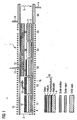
- the furnace 1 overall is composed of graphite, has a double-walled high-grade steel enclosure and, in accordance with Figure 1 , is subdivided into six successive segments S1...S6.
- locks 2, 3 in the form of gas curtains composed of an inert gas are provided on the inlet and outlet sides.
- the oxygen partial pressure in the furnace 1 must in any event be kept extremely low.
- the locks 2, 3 simultaneously enable substrates 4 to be transported by means of a transport device 5 through the individual segments S1...S6 of the furnace 1 in a continuous method.
- the transport device 5 in accordance with Figure 3 can comprise graphite rollers 6 which are mounted rotatably in the furnace 1 and on which the substrates 4 are pushed in segments longitudinally through the furnace 1.
- a displaceable and rotatable push rod 8 concomitantly provided with transport lugs 7 with the spacing pitch of the substrates 4 and equipped with a drive (not illustrated) is provided for this purpose.
- the transport lugs 7, before each transport travel are brought into engagement with the substrates 4 by rotation of the push rod 8 upwards and all the substrates 4 are accelerated simultaneously.
- the substrates 4 are braked, their leading edge engaging with the transport lug 7 of the respective preceding substrate 4.
- the transport lugs 7 are pivoted away again, whereupon the transport rod 8 is moved back to its starting position again.
- the residence duration of the substrates 4 in the individual segments S1...Sn is in each case identical and is 60 seconds, for example.
- the gas guiding in the interior of the furnace 1 is configured in such a way that all the gases and vapours supplied to the furnace 1 or arising in the latter are guided from the segment S1 via the following segments S2...Sn to an exhaust gas channel 9. Gas transport in the opposite direction is precluded.
- the furnace 1 contains six segments connected to one another via a continuous furnace channel, the segment S1 being temperature-regulated to an internal temperature of approximately 150°C, such that the substrates 4 introduced into the segment 1 are immediately subjected to a first heating process.
- the oxygen and hydrogen entrained into the segment S1 with the transport of the substrates 4 are also removed completely from the segment S1.
- the substrates are heated to a temperature of 400°C, and to approximately 500°C in the following segment S3, the temperature gradient varying from segment to segment in such a way that the heating rate is significantly higher, e.g. approximately twice as high, in the second section S2 than in the preceding section S1 and the succeeding section S3, until finally the end and reaction temperature is reached in the section S4 with 550°C. This reaction temperature is maintained in the succeeding section S5.
- Figure 1 illustrates adjacent to the section S5 a section S6, illustrated with an active cooling device 14 in the form of a water cooling. Since, in the event of excessively rapid cooling, thermally induced problems can occur with large-area substrates, it is also possible to insert an intermediate section without heating before the section S6, or to omit the cooling device of the section S6.
- metallic precursor layers 10 composed of copper, gallium and indium are situated on a molybdenum layer on the previously prepared substrates 4.
- substrates 4 comprising glass are firstly provided with a first molybdenum layer by sputtering, onto which layer are then sputtered a second layer composed of copper/gallium (CuGA) from a composite target and, finally, a third layer composed of indium from an indium target under a high vacuum ( Figure 1 ).
- a first molybdenum layer by sputtering, onto which layer are then sputtered a second layer composed of copper/gallium (CuGA) from a composite target and, finally, a third layer composed of indium from an indium target under a high vacuum ( Figure 1 ).
- CuGA copper/gallium
- the precursor layers are converted into a semiconducting CIGS layer in the segments S3-S5.
- This process requires firstly a temperature of 550°C in the segment S3 S5, and the presence of vaporous chalcogen, e.g. vaporous selenium.
- the substrates 4 are heated from 400°C to approximately 500°C in the segment S3 and to 550°C - 600°C in the segment S4 and a chalcogen vapour/carrier gas mixture is simultaneously conducted into the segments S3-S5 with sufficient concentration onto the surface of the substrates 4.
- the metallic precursor layer is converted abruptly into the desired semiconducting CIGS layer, after which the excess chalcogen vapour/carrier gas mixture is disposed of via the exhaust gas channel 9.
- the heating of the segments S1-S5 can be effected externally with the aid of an electrical or other heating 15 illustrated schematically in Figure 1 .
- the heating is then effected by the heated graphite walls, or in the segment S6, or in further segments the cooling is effected by, for example, cooled graphite walls of the furnace channel.
- chalcogen vapour/carrier gas mixture can be provided from an additional source 12.
- the substrates, prior to introduction into the furnace 1 have already been provided with a vapour-deposited chalcogen layer, which then evaporates in the segments S2 and S3 and is conducted by means of the internal gas guiding in the furnace 1 as chalcogen vapour 13, e.g. selenium vapour, into segment S4, and S5, where, if appropriate, residual chalcogen still present finally evaporates and is likewise available there for the conversion process.
- the conversion process is referred to as selenium annealing in the case where selenium vapour is used as the chalcogen.
- the two variants can also be combined with one another.
- An additional chalcogen vapour/carrier gas mixture can simultaneously be introduced into the segment S2, S3 or S3 if the concentration of the chalcogen evaporated from the substrates is insufficient ( Figure 1 ).
- the substrates 4 After a predetermined residence duration in the segment S5, generally 60 seconds, the substrates 4 are pushed into a further segment S6, in which cooling as rapidly as possible is effected by a cooling device 14, whereupon the substrates 4 are then discharged through a lock or pushed into a further segment S and from there discharged through a lock with a temperature of less than 100°C.
- the furnace 1 can also contain more than six segments, and that other temperature stipulations can also be set/chosen in the individual segments, provided that a temperature of 500-600°C is reached in the segment in which the metallic precursor layer is intended to be converted into the desired CIGS layer. A temperature of 550°C is a minimum here.
- the pressure in the furnace 1 can be at ambient pressure, e.g. at 1000 hPa.
Landscapes
- Chemical & Material Sciences (AREA)
- Chemical Kinetics & Catalysis (AREA)
- Engineering & Computer Science (AREA)
- Materials Engineering (AREA)
- Organic Chemistry (AREA)
- Mechanical Engineering (AREA)
- Metallurgy (AREA)
- Physics & Mathematics (AREA)
- Thermal Sciences (AREA)
- General Chemical & Material Sciences (AREA)
- Geochemistry & Mineralogy (AREA)
- Life Sciences & Earth Sciences (AREA)
- Photovoltaic Devices (AREA)
- Physical Vapour Deposition (AREA)
- Surface Treatment Of Glass (AREA)
- Chemical Vapour Deposition (AREA)
- Glass Compositions (AREA)
- Physical Or Chemical Processes And Apparatus (AREA)
- Physical Deposition Of Substances That Are Components Of Semiconductor Devices (AREA)
Description
- The present invention concerns a Method for thermally converting metallic precursor layers on substrates into semiconducting layers, and also an apparatus for carrying out the method and for producing solar modules on substrates.
- Such convertible metallic layers, which are also referred to as precursor layers, can contain copper, gallium and indium. The precursor layer can be applied to the substrate, which can be a glass substrate, by means of known technologies, e.g. by sputtering. For the conversion into semiconducting CIGS layers (CIGS: copper indium gallium selenide), so-called chalcogens, that is to say selenium, sulphur, tellurium and compounds thereof among one another or with other substances or mixtures thereof, have to be supplied onto said layers. At room temperature, that is to say around 20°C, said chalcogens assume a solid state of matter and evaporate at temperatures above approximately 350°C. Such glass substrates prepared with a CIGS layer can then be processed further as blanks to form solar modules, this including various contact-connections and, if appropriate, the application of passivations, filter layers, etc.
- What is essential for a good efficiency is for the precursor layer to be converted as completely as possible into the CIGS layer with an identical layer thickness over the area.
- According to the prior art, methods for thermally converting these prepared precursor layers into semiconducting layers have been disclosed which proceed either under vacuum, or else under atmospheric conditions with the supply of hydrogen-containing gases (
EP 0 318 315 A2 - The problem in the vacuum processes is the long conversion time (also called process time). In industrial conversion this leads to problems because long process times are always accompanied by low productivity. One solution would be, on the one hand, to use many machines simultaneously, but this would mean high costs in terms of capital expenditure, or else, on the other hand, to accelerate the processes. However, the prior art does not offer any indications in respect thereof.
-
EP 0 662 247 B1 -
EP 1 424 735 -
WO 2005/086238 describes a chamber having separated heating elements to anneal copper indium gallium diselenide solar cells. - The invention is based on the object, then, of providing an accelerated and simple-to-realize fast method for thermally converting metallic layers on any desired substrates into semiconducting layers, and also an apparatus suitable for carrying out the method and serving for producing solar modules with high efficiency.
- This is achieved by means of a method comprising the features of
claim 1. - The substrates previously prepared at least with a metallic precursor layer are heated in a furnace, which is segmented into different temperature regions, at a pressure at approximately atmospheric ambient pressure in a plurality of steps in each case to a predetermined temperature up to the end temperature between 400°C and 600°C and are converted into semiconducting layers whilst maintaining the end temperature in an atmosphere comprising a mixture of a carrier gas and vaporous chalcogens.
- The substrates are subsequently cooled to room temperature in at least one step.
- In one development of the invention, the substrate is previously prepared with a precursor layer and, above the latter, with a layer of chalcogens prior to introduction into the furnace.
- This chalcogen layer is preferably produced by vapour deposition of selenium onto the precursor layer.
- The invention is furthermore characterized in that the precursor layers are produced by successive sputtering of copper, indium and gallium.
- For this purpose, substrates comprising glass are firstly provided with a first molybdenum layer by sputtering, onto which layer are then sputtered a second layer composed of copper/gallium (CuGA) from a composite target and, finally, a third layer composed of indium from an indium target under a high vacuum.
- Furthermore, the heating of the substrates and the conversion of the precursor layers are performed in the absence of oxygen and hydrogen, or with a lowest possible oxygen partial pressure.
- After the conclusion of the conversion of the metallic precursor layers into CIGS layers, the substrate can also be cooled in a step-response function.
- In a further configuration of the invention, the substrates are transported step by step through the segmented furnace and are in each case heated to a higher temperature in successive segments, the predetermined residence duration in the individual segments being identical.
- The residence duration can be 60 seconds.
- Furthermore, the substrates are heated in the segments from room temperature, that is to say from an ambient temperature of approximately 20°C, with a decreasing temperature difference up to the end and reaction temperature, the temperature gradient varying from segment to segment in such a way that the heating rate is approximately twice as high in the second section as in the preceding section and the succeeding section, in which the end and reaction temperature is reached.
- As an alternative, the heating process can be effected in each section in a step-response function to the respective desired temperature.
- The heating can be performed in stages from room temperature to 150°C, 400°C and 500°C - 600°C, in which case the 550°C mark must not be exceeded as end temperature.
- The heating in the individual sections is performed over in each case an identical time duration, which can be 60 seconds.
- The substrates are cooled for example at a cooling rate of 8°C/sec.
- Furthermore, the pressure in the process chamber during the conversion process can be set to atmospheric pressure, e.g. to approximately 1000 hPa.
- A further configuration of the invention is characterized in that in the segment with the highest target temperature, a mixture of a chalcogen vapour/carrier gas mixture is brought over the surface of the substrate.
- The chalcogen vapour/carrier gas mixture can also be supplied from a heated source outside the muffle furnace.
- As an alternative, the chalcogen vapour/carrier gas mixture can contain vaporous chalcogen evaporated from the substrate in preceding segments.
- In a particular configuration of the invention, the chalcogen vapour/carrier gas mixture is produced from a mixture of chalcogen evaporated from the substrates in a preceding segment and additionally supplied chalcogen vapour from a source.
- A mixture of selenium vapour and nitrogen can be used as chalcogen vapour/carrier gas mixture.
- The object on which the invention is based is also achieved by means of an apparatus comprising the features of
claim 15. - Therein, the furnace is divided into a plurality of successive sections having different temperature regions, which are connected to one another by a continuous furnace channel, in which case, between an inlet-side section and an outlet-side section, further sections that can be heated independently of one another are arranged as heating zones and afterwards at least one section is arranged as a cooling zone. In the furnace channel that connects the sections there is situated a thermally and mechanically low-mass transport device for the step-by-step and simultaneous transport of all the substrates situated in the sections at a high speed from one section to the respective next section. The furnace is equipped with inlet- and outlet-side locks.
- Furthermore, the inlet-side section can be embodied as lock introduction chamber and the outlet-side section can be embodied as output lock.
- In one development of the invention, ambient pressure should prevail in the furnace.
- The transport device comprises graphite rollers which are mounted rotatably in the furnace and on which the substrates are guided displaceably in segments longitudinally through the furnace channel, and in that a displaceable and rotatable push rod concomitantly provided with transport lugs with the spacing pitch of the substrates is mounted between the rollers, the transport lugs of which, as viewed in the transport direction, can in each case be brought into engagement with the trailing edge of the substrates, it being possible for the leading edge of the substrates to be brought into engagement with the transport lug of the respective preceding substrate for braking purposes. The transport lugs can be brought into engagement by rotation of the push rod and, after transport travel has been effected, can be pivoted into a position out of engagement with the substrates.
- The residence duration of the substrates in the individual segments is identical and can be 60 seconds, for example.
- A further development of the invention is characterized in that the furnace is subdivided into six segments, it being possible for the segments to be temperature-regulated to different, respectively successively higher target temperatures; and a chalcogen vapour/carrier gas mixture with a predetermined concentration being situated in the segment having the highest target temperature.
- The target temperatures are graded in the individual segments in such a way that a target temperature of for example 150°C can be set in the first segment, a target temperature of 400°C can be set in the following segment, and a target temperature of 550°C can be set in the next segment, for the substrates.
- Furthermore, the segment following the segment having the highest target temperature is connected to an exhaust gas channel for discharging and conditioning excess chalcogen vapour/carrier gas mixture.
- Finally, the inlet- and outlet-side locks comprise gas curtains that ensure that the interior of the furnace is sufficiently sealed with respect to oxygen and hydrogen.
- A solar module comprising a CIGS layer on a substrate, can be produced by providing a substrate prepared with a metallic precursor layer, heating the substrate in a plurality of stages to in each case a higher target temperature with different temperature gradients up to the conversion temperature of 550°C for converting the precursor layer into a CIGS layer with a vaporous chalcogen applied to the precursor layer.
- The cooling can be effected for example in a step-response function or at a cooling rate of approximately 8-10°C/second.
- The temperature gradient varies from segment to segment in such a way that the heating rate is approximately twice as high in the second section as in the preceding section and the succeeding section, in which the end and reaction temperature is reached.
- The method according to the invention achieves a particularly uniform lattice structure of the CIGS layer in association with a higher efficiency of the solar module.
- Preferably, vaporous selenium, sulphur, tellurium, compounds thereof among one another or with other substances or mixtures thereof are used as the chalcogen.
- Furthermore, the metallic precursor layers contain copper, indium and gallium.
- The invention realizes an accelerated method for converting the metallic layers into semiconducting layers.
- It has been shown that the processes for converting the metallic layers into semiconducting layers depend both on the temperature and on the ambient pressure. Although it is generally known that chemical reactions - the conversion of the metallic layers to semiconducting semiconductor layers being such a chemical reaction - are a function of temperature and of pressure, the temperature dependence of the reactions has always been utilized heretofore for the present problem, which can be regarded as an indication that experts have not taken into account, that is to say have overlooked, the variation of the process pressure with regard to the conversion of metallic layers into semiconducting layers.
- Advantages of the present method are a faster conversion of metallic layers into semiconducting layers, shorter cycle times in the industrial process and a more cost-effective fabrication since lower capital expenditure arises owing to fewer installations required.
- The present invention concerns a novel thermal process for any desired substrates in which metallic layers, which can contain copper, gallium and indium, are converted with selenium and/or sulphur into semiconducting semiconductor layers. The conversion is effected at ambient or atmospheric pressure.
- The special feature of the present invention is that rather than working under vacuum, work is performed under atmospheric conditions, or under increased process pressure, whereby the speed of the chemical reactions involved in the conversion is considerably increased.
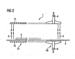
- The invention will be explained in more detail below on the basis of an exemplary embodiment. The associated drawings showing not true to scale:
- Figure 1
- a schematic illustration of a furnace that is divided into a plurality of segments and is suitable for the step-by-step transport of substrates;
- Figure 2
- schematically illustrated details of the furnace according to
Figure 1 ; and - Figure 3
- a schematic plan view of the transport device.
- The method according to the invention for thermally converting metallic layers, which can contain copper, gallium or indium, on substrates into semiconducting CIGS layers can be performed per se in any desired
furnace 1, e.g. a muffle furnace, which has to meet the following preconditions. - The
furnace 1 must comprise heatable or coolable segments S1...Sn, of which the heatable segments S1...Sn must be suitable at least in part for carrying out fast thermal processes. - Furthermore, the
furnace 1 must be able to be operated under atmospheric pressure and must be provided with suitable devices for feeding in and discharging gas. - A further important recondition is that care is taken to ensure that the interior of the
furnace 1, over the entire length thereof, is constantly kept largely free of oxygen and, if appropriate, also of hydrogen. - The
furnace 1 overall is composed of graphite, has a double-walled high-grade steel enclosure and, in accordance withFigure 1 , is subdivided into six successive segments S1...S6. - In order to keep the interior of the
furnace 1 free of oxygen and hydrogen, locks 2, 3 in the form of gas curtains composed of an inert gas are provided on the inlet and outlet sides. The oxygen partial pressure in thefurnace 1 must in any event be kept extremely low. Thelocks 2, 3 simultaneously enablesubstrates 4 to be transported by means of atransport device 5 through the individual segments S1...S6 of thefurnace 1 in a continuous method. - The
transport device 5 in accordance withFigure 3 can comprisegraphite rollers 6 which are mounted rotatably in thefurnace 1 and on which thesubstrates 4 are pushed in segments longitudinally through thefurnace 1. A displaceable and rotatable push rod 8 concomitantly provided withtransport lugs 7 with the spacing pitch of thesubstrates 4 and equipped with a drive (not illustrated) is provided for this purpose. - In order to carry out the transport of all the
substrates 4 simultaneously, the transport lugs 7, before each transport travel, are brought into engagement with thesubstrates 4 by rotation of the push rod 8 upwards and all thesubstrates 4 are accelerated simultaneously. At the end of each transport travel, thesubstrates 4 are braked, their leading edge engaging with thetransport lug 7 of the respective precedingsubstrate 4. After the transport travel has been effected, the transport lugs 7 are pivoted away again, whereupon the transport rod 8 is moved back to its starting position again. - The residence duration of the
substrates 4 in the individual segments S1...Sn is in each case identical and is 60 seconds, for example. - The gas guiding in the interior of the
furnace 1 is configured in such a way that all the gases and vapours supplied to thefurnace 1 or arising in the latter are guided from the segment S1 via the following segments S2...Sn to anexhaust gas channel 9. Gas transport in the opposite direction is precluded. - In accordance with
Figure 1 , thefurnace 1 contains six segments connected to one another via a continuous furnace channel, the segment S1 being temperature-regulated to an internal temperature of approximately 150°C, such that thesubstrates 4 introduced into thesegment 1 are immediately subjected to a first heating process. In this segment, the oxygen and hydrogen entrained into the segment S1 with the transport of thesubstrates 4 are also removed completely from the segment S1. - In the next segment S2, the substrates are heated to a temperature of 400°C, and to approximately 500°C in the following segment S3, the temperature gradient varying from segment to segment in such a way that the heating rate is significantly higher, e.g. approximately twice as high, in the second section S2 than in the preceding section S1 and the succeeding section S3, until finally the end and reaction temperature is reached in the section S4 with 550°C. This reaction temperature is maintained in the succeeding section S5.
-
Figure 1 illustrates adjacent to the section S5 a section S6, illustrated with anactive cooling device 14 in the form of a water cooling. Since, in the event of excessively rapid cooling, thermally induced problems can occur with large-area substrates, it is also possible to insert an intermediate section without heating before the section S6, or to omit the cooling device of the section S6. - As will be explained in more detail below, metallic precursor layers 10 composed of copper, gallium and indium are situated on a molybdenum layer on the previously
prepared substrates 4. - For this purpose,
substrates 4 comprising glass are firstly provided with a first molybdenum layer by sputtering, onto which layer are then sputtered a second layer composed of copper/gallium (CuGA) from a composite target and, finally, a third layer composed of indium from an indium target under a high vacuum (Figure 1 ). - The precursor layers are converted into a semiconducting CIGS layer in the segments S3-S5. This process requires firstly a temperature of 550°C in the segment S3 S5, and the presence of vaporous chalcogen, e.g. vaporous selenium.
- For this purpose, by way of example, the
substrates 4 are heated from 400°C to approximately 500°C in the segment S3 and to 550°C - 600°C in the segment S4 and a chalcogen vapour/carrier gas mixture is simultaneously conducted into the segments S3-S5 with sufficient concentration onto the surface of thesubstrates 4. In this case, the metallic precursor layer is converted abruptly into the desired semiconducting CIGS layer, after which the excess chalcogen vapour/carrier gas mixture is disposed of via theexhaust gas channel 9. - The heating of the segments S1-S5 can be effected externally with the aid of an electrical or
other heating 15 illustrated schematically inFigure 1 . Within thefurnace 1, the heating is then effected by the heated graphite walls, or in the segment S6, or in further segments the cooling is effected by, for example, cooled graphite walls of the furnace channel. - There are various possibilities for producing the necessary chalcogen concentration in the segments S3-S5. Thus, a chalcogen vapour/carrier gas mixture can be provided from an
additional source 12. Another possibility is that the substrates, prior to introduction into thefurnace 1, have already been provided with a vapour-deposited chalcogen layer, which then evaporates in the segments S2 and S3 and is conducted by means of the internal gas guiding in thefurnace 1 aschalcogen vapour 13, e.g. selenium vapour, into segment S4, and S5, where, if appropriate, residual chalcogen still present finally evaporates and is likewise available there for the conversion process. - The conversion process is referred to as selenium annealing in the case where selenium vapour is used as the chalcogen. As an alternative, the two variants can also be combined with one another. An additional chalcogen vapour/carrier gas mixture can simultaneously be introduced into the segment S2, S3 or S3 if the concentration of the chalcogen evaporated from the substrates is insufficient (
Figure 1 ). - After a predetermined residence duration in the segment S5, generally 60 seconds, the
substrates 4 are pushed into a further segment S6, in which cooling as rapidly as possible is effected by acooling device 14, whereupon thesubstrates 4 are then discharged through a lock or pushed into a further segment S and from there discharged through a lock with a temperature of less than 100°C. - It goes without saying that the
furnace 1 can also contain more than six segments, and that other temperature stipulations can also be set/chosen in the individual segments, provided that a temperature of 500-600°C is reached in the segment in which the metallic precursor layer is intended to be converted into the desired CIGS layer. A temperature of 550°C is a minimum here. - The pressure in the
furnace 1 can be at ambient pressure, e.g. at 1000 hPa. - What is crucial for the process control is the interplay between the transport of the
substrates 4 through thefurnace 1 from segment to segment through the furnace channel. In this case, it must be ensured that enough vaporous chalcogens, e.g. selenium vapour, are present in the furnace atmosphere above thesubstrates 4 in the segment S4 when the reaction temperature is reached. Only then can an abrupt conversion of copper/gallium and indium of theprecursor layer 10 to CIGS take place. This is also achieved by each segment S1-S6 being equipped at any time with onesubstrate 4 or a plurality of substrates alongside one another, such that this can be designated as quasi-continuous operation of thefurnace 1. -
- 1
- Furnace
- 2
- Inlet-side flow lock
- 3
- Outlet-side flow lock
- 4
- Substrate
- 5
- Transport device
- 6
- Graphite roller
- 7
- Transport lug*
- 8
- Push rod
- 9
- Exhaust gas channel
- 10
- Precursor layer
- 11
- CIGS layer
- 12
- Source
- 13
- Chalcogen vapour
- 14
- Cooling device
- 15
- Heating
Claims (20)
- Method for thermally converting metallic precursor layers on a substrate into semiconducting layers, wherein the substrates (4) prepared at least with a metallic precursor layer (10) are heated in a furnace (1), which is segmented into a plurality of temperature regions, to an end temperature between 400 °C and 600 °C and are converted into semiconducting layers whilst maintaining the end temperature in an atmosphere comprising vaporous chalcogens,
characterized- in that the substrates (4) are prepared with the metallic precursor layer (10) before they are heated in the furnace (1),- in that the substrates (4) are heated in the furnace (1) at a pressure at approximately atmospheric ambient pressure in a plurality of steps in each case to a predetermined temperature up to the end temperature,- in that the atmosphere in which the substrates (4) are converted into semiconducting layers comprises a mixture of a carrier gas and vaporous chalcogens, and- in that a push rod (8) is rotated in order to bring transport lugs (7) of the push rod (8) into engagement with the substrates (4), the push rod (8) is then accelerated and in doing so the substrates (4) are transported simultaneously through the segmented furnace (1). - Method according to Claim 1,
characterized in that
the substrates (4) are subsequently cooled to room temperature in at least one step. - Method according to Claim 1,
characterized in that
the substrate (4) is previously prepared with a precursor layer (10) and, above the latter, with a layer of chalcogens prior to introduction into the furnace (1). - Method according to Claim 3,
characterized in that
the chalcogen layer is produced principally by vapour deposition of selenium onto the precursor layer (10). - Method according to Claims 1 to 4,
characterized in that
the precursor layer (10) is produced in a preceding process by successive sputtering of copper, indium and gallium. - Method according to Claim 5,
characterized in that
substrates (4) comprising glass are firstly provided with a first molybdenum layer by sputtering, onto which layer are then sputtered a second layer composed of copper/gallium from a composite target and, finally, a third layer composed of indium from an indium target under high vacuum. - Method according to Claim 1,
characterized in that
the heating of the substrates (4) and the conversion of the precursor layer (10) into a CIGS layer are performed in the absence of oxygen and hydrogen. - Method according to any of Claims 1 to 7,
characterized in that
the substrates (4) are transported step by step through a segmented furnace (1) and are in each case heated to a higher temperature in successive segments (S1 ... Sn), the predetermined residence duration in the individual segments (S1 .... Sn) being identical. - Method according to any of Claims 1 to 8,
chararacterized in that
the heating is effected in stages from room temperature to 150 °C, 400 °C and 500 °C to 600 °C, or at least 550 °C. - Method according to any of Claims 1 to 9,
characterized in that
the heating to the next higher temperature in the individual sections is effected over in each case an identical time duration, which can be 60 seconds. - Method according to any of Claims 1 to 10,
characterized in that
atmospheric pressure is set, e. g. to 1000 hPa, in the furnace (1) during the conversion process. - Method according to any of Claims 1 to 11,
characterized in that
in the segment with the highest target temperature, a mixture of a chalcogen vapour/carrier gas mixture is brought over the surface of the substrate, and in that the chalcogens vapour/carrier gas mixture is supplied from a source. - Method according to any of Claims 1 to 12,
characterized in that
in the segment with the highest target temperature, a mixture of a chalcogen vapour/carrier gas mixture is brought over the surface of the substrate, and in that the chalcogen vapour/carrier gas mixture contains vaporous chalcogen evaporated from the substrate in preceding segments. - Method according to any of Claims 1 to 13,
characterized in that
a mixture of selenium vapour and nitrogen is used as chalcogen vapour/carrier gas mixture. - Apparatus for carrying out the method in a furnace, wherein the furnace (1) is divided into a plurality of successive sections (S1 ... Sn) having different temperature which are connected to one another by a continuous furnace channel, in which case, between an inlet-side section (S1) and an outlet-side section (Sn), further sections that can be heated independently of one another are arranged as heating zones and a transport device (5) for simultaneous transport of all substrates (4) situated in the sections (S1 ... Sn) from one section (S1 ... Sn) to the respective next section (S1 ... Sn) is provided,
characterized- in that at least one section is arranged as a cooling zone after the further sections,- in that the furnace (1) is equipped with inlet- and outlet-side locks (2, 3),- in that the transport device (5) has a particularly low thermal and mechanical mass and is situated in the furnace channel that connects the sections (S1 -. Sn),- in that the substrates (4) can be transported step-by-step by means of the transport device (5),- in that the transport device (5) comprises graphite rollers (6) which are mounted rotatably in the furnace (1) and on which the substrates (4) are guided displaceably in segments longitudinally through the furnace (1), and- in that for transport of the substrates (4) at a particular high speed a displaceable and rotatable push rod (8) concomitantly provided with transport lugs (7) with the spacing pitch of the substrates (4) is mounted between the rollers (6), the transport lugs (7) of which, as viewed in the transport direction, can in each case be brought into engagement with the trailing edge of the substrates (4). - Apparatus according to Claim 15,
characterized in that
the inlet-side section is embodied as a lock introduction chamber and the outlet-side section is embodied as output lock. - Apparatus according to any of Claims 15 to 16,
characterized in that
ambient pressure prevails in the furnace (1). - Apparatus according to any of Claims 15 to 17,
characterized in that
the transport lugs (7) can be brought into engagement by rotation of the push rod (8) and, after transport travel has been effected, can be pivoted into a position out of engagement with the substrates (4). - Apparatus according to any of Claims 15 to 18,
characterized in that
the segment (S6) following the segment having the highest desired temperature is connected to an exhaust gas channel (9) for discharging excess chalcogen vapour/carrier gas mixture. - Apparatus according to any of Claims 15 to 19,
characterised in that
the inlet- and outlet-side locks (2, 3) comprise gas curtains.
Applications Claiming Priority (5)
| Application Number | Priority Date | Filing Date | Title |
|---|---|---|---|
| DE102007043051 | 2007-09-11 | ||
| DE102007047098 | 2007-10-01 | ||
| DE102007047099 | 2007-10-01 | ||
| DE102007048204 | 2007-10-08 | ||
| PCT/EP2008/007466 WO2009033674A2 (en) | 2007-09-11 | 2008-09-11 | Method and apparatus for thermally converting metallic precursor layers into semiconducting layers, and also solar module |
Publications (2)
| Publication Number | Publication Date |
|---|---|
| EP2205773A2 EP2205773A2 (en) | 2010-07-14 |
| EP2205773B1 true EP2205773B1 (en) | 2014-11-12 |
Family
ID=40380095
Family Applications (2)
| Application Number | Title | Priority Date | Filing Date |
|---|---|---|---|
| EP08804026A Withdrawn EP2205772A2 (en) | 2007-09-11 | 2008-09-11 | Method and arrangement for providing chalcogens |
| EP08830338.3A Not-in-force EP2205773B1 (en) | 2007-09-11 | 2008-09-11 | Method and apparatus for thermally converting metallic precursor layers into semiconducting layers |
Family Applications Before (1)
| Application Number | Title | Priority Date | Filing Date |
|---|---|---|---|
| EP08804026A Withdrawn EP2205772A2 (en) | 2007-09-11 | 2008-09-11 | Method and arrangement for providing chalcogens |
Country Status (7)
| Country | Link |
|---|---|
| US (3) | US20100203668A1 (en) |
| EP (2) | EP2205772A2 (en) |
| JP (2) | JP2010539323A (en) |
| KR (2) | KR20100052429A (en) |
| AU (2) | AU2008297944A1 (en) |
| TW (2) | TWI555864B (en) |
| WO (2) | WO2009034131A2 (en) |
Families Citing this family (34)
| Publication number | Priority date | Publication date | Assignee | Title |
|---|---|---|---|---|
| DE102009009022A1 (en) | 2009-02-16 | 2010-08-26 | Centrotherm Photovoltaics Ag | Method and device for coating flat substrates with chalcogens |
| DE102009011496A1 (en) | 2009-03-06 | 2010-09-16 | Centrotherm Photovoltaics Ag | Process and device for the thermal conversion of metallic precursor layers into semiconducting layers with chalcogen recovery |
| DE102009012200A1 (en) | 2009-03-11 | 2010-09-16 | Centrotherm Photovoltaics Ag | Thermal conversion of metallic precursor layer into semiconductor layer in thin layer solar cell, involves introducing chalcogen vapor/carrier gas mixture on substrate having precursor layer, heating, converting and cooling |
| DE102009011695A1 (en) | 2009-03-09 | 2010-09-16 | Centrotherm Photovoltaics Ag | Thermal conversion of metallic precursor layer into semiconductor layer in thin layer solar cell, involves introducing chalcogen vapor/carrier gas mixture on substrate having precursor layer, heating, converting and cooling |
| KR101245371B1 (en) * | 2009-06-19 | 2013-03-19 | 한국전자통신연구원 | Solar cell and method of fabricating the same |
| EP2278625A1 (en) | 2009-07-24 | 2011-01-26 | centrotherm photovoltaics AG | Method and apparatus for deposition of a layer of an Indium Chalcogenide onto a substrate |
| JP2013504215A (en) * | 2009-09-02 | 2013-02-04 | ボルマン、ブレント | Methods and devices for processing precursor layers in a Group VIA environment |
| IT1395908B1 (en) | 2009-09-17 | 2012-11-02 | Advanced Res On Pv Tech S R L | PROCESS FOR THE PRODUCTION OF SOLAR FILMS WITH THIN FILMS CU (IN, GA) SE2 / CDS |
| FR2951022B1 (en) * | 2009-10-07 | 2012-07-27 | Nexcis | MANUFACTURE OF THIN LAYERS WITH PHOTOVOLTAIC PROPERTIES, BASED ON TYPE I-III-VI2 ALLOY, BY SUCCESSIVE ELECTRO-DEPOSITS AND THERMAL POST-TREATMENT. |
| DE102009053532B4 (en) | 2009-11-18 | 2017-01-05 | Centrotherm Photovoltaics Ag | Method and apparatus for producing a compound semiconductor layer |
| EP2369034B1 (en) | 2010-03-26 | 2013-01-30 | Saint-Gobain Glass France | Method for refilling a selenium evaporation chamber |
| EP2369033A1 (en) | 2010-03-26 | 2011-09-28 | Saint-Gobain Glass France | Method for refilling an evaporation chamber |
| EP2371991B1 (en) | 2010-03-26 | 2013-01-30 | Saint-Gobain Glass France | Method for discontinuous refilling of a selenium evaporation chamber |
| DE102010018595A1 (en) | 2010-04-27 | 2011-10-27 | Centrothem Photovoltaics Ag | Process for producing a compound semiconductor layer |
| JP2012015323A (en) * | 2010-06-30 | 2012-01-19 | Fujifilm Corp | Method of manufacturing cis-based film |
| JP2012015328A (en) * | 2010-06-30 | 2012-01-19 | Fujifilm Corp | Manufacturing method of cis-based film |
| JP2012015314A (en) * | 2010-06-30 | 2012-01-19 | Fujifilm Corp | Manufacturing method of cis-based film |
| DE102010034653A1 (en) | 2010-08-17 | 2012-02-23 | Centrotherm Photovoltaics Ag | Process for the condensation of chalcogen vapor and apparatus for carrying out the process |
| DE102010035569A1 (en) | 2010-08-26 | 2012-03-01 | Centrotherm Photovoltaics Ag | Continuous furnace |
| WO2012025607A1 (en) * | 2010-08-27 | 2012-03-01 | Saint-Gobain Glass France | Device and method for heat-treating a plurality of multi-layer bodies |
| KR20140007332A (en) * | 2010-09-15 | 2014-01-17 | 프리커서 에너제틱스, 인코퍼레이티드. | Inks with alkali metals for thin film solar cell processes |
| KR101371077B1 (en) * | 2011-03-30 | 2014-03-07 | 씨디에스(주) | Apparatus for forming thin film |
| TW201250017A (en) * | 2011-06-08 | 2012-12-16 | Ind Tech Res Inst | Method and apparatus for depositing selenium thin-film and plasma head thereof |
| JP5709730B2 (en) * | 2011-11-15 | 2015-04-30 | 京セラ株式会社 | Thin film manufacturing method |
| WO2013125818A1 (en) * | 2012-02-24 | 2013-08-29 | 영남대학교 산학협력단 | Solar cell manufacturing apparatus and solar cell manufacturing method |
| US20130309848A1 (en) | 2012-05-16 | 2013-11-21 | Alliance For Sustainable Energy, Llc | High throughput semiconductor deposition system |
| WO2014095503A1 (en) | 2012-12-20 | 2014-06-26 | Saint-Gobain Glass France | Method for producing a compound semiconductor, and thin-film solar cell |
| US10317139B2 (en) * | 2013-10-09 | 2019-06-11 | United Technologies Corporation | Method and apparatus for processing process-environment-sensitive material |
| DE102013113108B4 (en) * | 2013-11-27 | 2024-08-29 | Hanwha Q Cells Gmbh | Solar cell manufacturing process |
| CN105363397A (en) * | 2014-08-19 | 2016-03-02 | 姚小兵 | Steam system |
| TWI550717B (en) | 2014-08-25 | 2016-09-21 | 新能光電科技股份有限公司 | Heat treatment method and product obtained thereby |
| TWI617684B (en) * | 2016-10-07 | 2018-03-11 | 國家中山科學研究院 | Integrated fast selenium vulcanization process equipment |
| US10190234B1 (en) | 2017-10-30 | 2019-01-29 | Wisconsin Alumni Research Foundation | Continuous system for fabricating multilayer heterostructures via hydride vapor phase epitaxy |
| TWI689455B (en) * | 2019-07-30 | 2020-04-01 | 群翊工業股份有限公司 | Nitrogen box capable of preventing board deviation from continuous passage |
Family Cites Families (17)
| Publication number | Priority date | Publication date | Assignee | Title |
|---|---|---|---|---|
| US2426377A (en) * | 1943-12-07 | 1947-08-26 | Ruben Samuel | Selenium rectifier and method of making |
| JPS5320950B2 (en) * | 1972-07-12 | 1978-06-29 | ||
| US4576830A (en) * | 1984-11-05 | 1986-03-18 | Chronar Corp. | Deposition of materials |
| US5248349A (en) * | 1992-05-12 | 1993-09-28 | Solar Cells, Inc. | Process for making photovoltaic devices and resultant product |
| US6202591B1 (en) * | 1998-11-12 | 2001-03-20 | Flex Products, Inc. | Linear aperture deposition apparatus and coating process |
| US6143080A (en) * | 1999-02-02 | 2000-11-07 | Silicon Valley Group Thermal Systems Llc | Wafer processing reactor having a gas flow control system and method |
| JP2001049432A (en) * | 1999-08-02 | 2001-02-20 | Sony Corp | Work movable reactive sputtering apparatus and work movable reactive sputtering method |
| DE60237159D1 (en) * | 2001-07-06 | 2010-09-09 | Honda Motor Co Ltd | METHOD FOR FORMING A LIGHT ABSORBING LAYER |
| JP2005133122A (en) * | 2003-10-29 | 2005-05-26 | Sony Corp | Film forming apparatus and film forming method |
| SE0400582D0 (en) | 2004-03-05 | 2004-03-05 | Forskarpatent I Uppsala Ab | Method for in-line process control of the CIGS process |
| MX2007013335A (en) * | 2005-04-26 | 2008-03-24 | First Solar Inc | System and method for depositing a material on a substrate. |
| US7931937B2 (en) * | 2005-04-26 | 2011-04-26 | First Solar, Inc. | System and method for depositing a material on a substrate |
| US7955031B2 (en) * | 2005-07-06 | 2011-06-07 | First Solar, Inc. | Material supply system and method |
| US20070111367A1 (en) * | 2005-10-19 | 2007-05-17 | Basol Bulent M | Method and apparatus for converting precursor layers into photovoltaic absorbers |
| BRPI0710139A2 (en) * | 2006-04-14 | 2011-08-23 | Silica Tech Llc | PLASMA DEPOSITION APPARATUS TO MAKE SOLAR CELLS, AND, METHOD FOR FORMING A SOLAR CELL LAYER |
| JP2008011467A (en) * | 2006-06-30 | 2008-01-17 | Toshiba Corp | Display panel imaging method and display panel imaging apparatus |
| JP2010509779A (en) * | 2006-11-10 | 2010-03-25 | ソロパワー、インコーポレイテッド | Open reel reaction of precursor film to form solar cell absorber |
-
2008
- 2008-09-11 EP EP08804026A patent/EP2205772A2/en not_active Withdrawn
- 2008-09-11 TW TW097134932A patent/TWI555864B/en not_active IP Right Cessation
- 2008-09-11 JP JP2010523539A patent/JP2010539323A/en not_active Withdrawn
- 2008-09-11 US US12/528,913 patent/US20100203668A1/en not_active Abandoned
- 2008-09-11 JP JP2010523359A patent/JP2010539679A/en not_active Withdrawn
- 2008-09-11 EP EP08830338.3A patent/EP2205773B1/en not_active Not-in-force
- 2008-09-11 KR KR1020097021149A patent/KR20100052429A/en not_active Withdrawn
- 2008-09-11 KR KR1020097021552A patent/KR20100051586A/en not_active Withdrawn
- 2008-09-11 US US12/529,872 patent/US20100151129A1/en not_active Abandoned
- 2008-09-11 AU AU2008297944A patent/AU2008297944A1/en not_active Abandoned
- 2008-09-11 AU AU2008297124A patent/AU2008297124A1/en not_active Abandoned
- 2008-09-11 TW TW097134931A patent/TWI424073B/en not_active IP Right Cessation
- 2008-09-11 WO PCT/EP2008/062061 patent/WO2009034131A2/en not_active Ceased
- 2008-09-11 WO PCT/EP2008/007466 patent/WO2009033674A2/en not_active Ceased
-
2015
- 2015-08-12 US US14/824,806 patent/US20150368789A1/en not_active Abandoned
Also Published As
| Publication number | Publication date |
|---|---|
| WO2009034131A2 (en) | 2009-03-19 |
| JP2010539679A (en) | 2010-12-16 |
| TWI555864B (en) | 2016-11-01 |
| EP2205772A2 (en) | 2010-07-14 |
| KR20100052429A (en) | 2010-05-19 |
| AU2008297124A1 (en) | 2009-03-19 |
| TW200914634A (en) | 2009-04-01 |
| TW200914633A (en) | 2009-04-01 |
| AU2008297944A1 (en) | 2009-03-19 |
| US20150368789A1 (en) | 2015-12-24 |
| EP2205773A2 (en) | 2010-07-14 |
| TWI424073B (en) | 2014-01-21 |
| WO2009034131A3 (en) | 2009-05-22 |
| US20100151129A1 (en) | 2010-06-17 |
| WO2009033674A3 (en) | 2009-05-22 |
| US20100203668A1 (en) | 2010-08-12 |
| WO2009033674A2 (en) | 2009-03-19 |
| JP2010539323A (en) | 2010-12-16 |
| KR20100051586A (en) | 2010-05-17 |
Similar Documents
| Publication | Publication Date | Title |
|---|---|---|
| US20100203668A1 (en) | Method and apparatus for thermally converting metallic precursor layers into semiconducting layers, and also solar module | |
| EP1424735B1 (en) | Method for forming light-absorbing layer | |
| EP2291868B1 (en) | Device and method for tempering objects in a treatment chamber | |
| US20100226629A1 (en) | Roll-to-roll processing and tools for thin film solar cell manufacturing | |
| US9111980B2 (en) | Gas exhaust for high volume, low cost system for epitaxial silicon deposition | |
| US20160064593A1 (en) | METHOD AND APPARATUS FOR DEPOSITING COPPER-INDIUM-GALLIUM SELENIDE (CuInGaSe2-CIGS) THIN FILMS AND OTHER MATERIALS ON A SUBSTRATE | |
| US20090183675A1 (en) | Reactor to form solar cell absorbers | |
| WO2011146301A1 (en) | Chalcogenide-based materials and methods of making such materials under vacuum using post-chalcogenization techniques | |
| KR20090110293A (en) | Reel-to-Reel Reaction of Precursor to Form Cell Absorber | |
| CN101668877B (en) | Method and apparatus for thermally converting metallic precursor layers into semiconducting layers, and also solar module | |
| WO2010100560A1 (en) | Process and device for the thermal conversion of metallic precursor layers into semiconducting layers with chalcogen recovery | |
| KR101284760B1 (en) | Rapid thermal process apparatus for solar cell and processing method using thereof | |
| US20120289033A1 (en) | Method and device for producing a compound semiconductor layer | |
| US20120034734A1 (en) | System and method for fabricating thin-film photovoltaic devices | |
| DE102009011695A1 (en) | Thermal conversion of metallic precursor layer into semiconductor layer in thin layer solar cell, involves introducing chalcogen vapor/carrier gas mixture on substrate having precursor layer, heating, converting and cooling | |
| WO2010078088A1 (en) | Reactor to form solar cell absorbers in roll-to-roll fashion | |
| WO2011135420A1 (en) | Process for the production of a compound semiconductor layer | |
| RU2354006C1 (en) | METHOD FOR PRODUCTION OF THIN FILM OF COPPER AND INDIUM DISELENIDE CuInSe2 | |
| JP2005116755A (en) | Solar cell manufacturing equipment | |
| JP2012015323A (en) | Method of manufacturing cis-based film |
Legal Events
| Date | Code | Title | Description |
|---|---|---|---|
| PUAI | Public reference made under article 153(3) epc to a published international application that has entered the european phase |
Free format text: ORIGINAL CODE: 0009012 |
|
| 17P | Request for examination filed |
Effective date: 20100517 |
|
| AK | Designated contracting states |
Kind code of ref document: A2 Designated state(s): AT BE BG CH CY CZ DE DK EE ES FI FR GB GR HR HU IE IS IT LI LT LU LV MC MT NL NO PL PT RO SE SI SK TR |
|
| AX | Request for extension of the european patent |
Extension state: AL BA MK RS |
|
| RIN1 | Information on inventor provided before grant (corrected) |
Inventor name: SCHMID, DIETER Inventor name: HARTUNG, ROBERT, MICHAEL Inventor name: LENZ, REINHARD |
|
| DAX | Request for extension of the european patent (deleted) | ||
| 17Q | First examination report despatched |
Effective date: 20130724 |
|
| GRAP | Despatch of communication of intention to grant a patent |
Free format text: ORIGINAL CODE: EPIDOSNIGR1 |
|
| INTG | Intention to grant announced |
Effective date: 20140303 |
|
| GRAP | Despatch of communication of intention to grant a patent |
Free format text: ORIGINAL CODE: EPIDOSNIGR1 |
|
| INTG | Intention to grant announced |
Effective date: 20140605 |
|
| GRAS | Grant fee paid |
Free format text: ORIGINAL CODE: EPIDOSNIGR3 |
|
| GRAA | (expected) grant |
Free format text: ORIGINAL CODE: 0009210 |
|
| AK | Designated contracting states |
Kind code of ref document: B1 Designated state(s): AT BE BG CH CY CZ DE DK EE ES FI FR GB GR HR HU IE IS IT LI LT LU LV MC MT NL NO PL PT RO SE SI SK TR |
|
| REG | Reference to a national code |
Ref country code: GB Ref legal event code: FG4D |
|
| REG | Reference to a national code |
Ref country code: CH Ref legal event code: EP |
|
| REG | Reference to a national code |
Ref country code: AT Ref legal event code: REF Ref document number: 695828 Country of ref document: AT Kind code of ref document: T Effective date: 20141115 |
|
| REG | Reference to a national code |
Ref country code: IE Ref legal event code: FG4D |
|
| REG | Reference to a national code |
Ref country code: DE Ref legal event code: R096 Ref document number: 602008035356 Country of ref document: DE Effective date: 20141224 |
|
| REG | Reference to a national code |
Ref country code: NL Ref legal event code: T3 |
|
| REG | Reference to a national code |
Ref country code: AT Ref legal event code: MK05 Ref document number: 695828 Country of ref document: AT Kind code of ref document: T Effective date: 20141112 |
|
| PG25 | Lapsed in a contracting state [announced via postgrant information from national office to epo] |
Ref country code: PT Free format text: LAPSE BECAUSE OF FAILURE TO SUBMIT A TRANSLATION OF THE DESCRIPTION OR TO PAY THE FEE WITHIN THE PRESCRIBED TIME-LIMIT Effective date: 20150312 Ref country code: ES Free format text: LAPSE BECAUSE OF FAILURE TO SUBMIT A TRANSLATION OF THE DESCRIPTION OR TO PAY THE FEE WITHIN THE PRESCRIBED TIME-LIMIT Effective date: 20141112 Ref country code: LT Free format text: LAPSE BECAUSE OF FAILURE TO SUBMIT A TRANSLATION OF THE DESCRIPTION OR TO PAY THE FEE WITHIN THE PRESCRIBED TIME-LIMIT Effective date: 20141112 Ref country code: FI Free format text: LAPSE BECAUSE OF FAILURE TO SUBMIT A TRANSLATION OF THE DESCRIPTION OR TO PAY THE FEE WITHIN THE PRESCRIBED TIME-LIMIT Effective date: 20141112 Ref country code: NO Free format text: LAPSE BECAUSE OF FAILURE TO SUBMIT A TRANSLATION OF THE DESCRIPTION OR TO PAY THE FEE WITHIN THE PRESCRIBED TIME-LIMIT Effective date: 20150212 Ref country code: IS Free format text: LAPSE BECAUSE OF FAILURE TO SUBMIT A TRANSLATION OF THE DESCRIPTION OR TO PAY THE FEE WITHIN THE PRESCRIBED TIME-LIMIT Effective date: 20150312 |
|
| PG25 | Lapsed in a contracting state [announced via postgrant information from national office to epo] |
Ref country code: HR Free format text: LAPSE BECAUSE OF FAILURE TO SUBMIT A TRANSLATION OF THE DESCRIPTION OR TO PAY THE FEE WITHIN THE PRESCRIBED TIME-LIMIT Effective date: 20141112 Ref country code: LV Free format text: LAPSE BECAUSE OF FAILURE TO SUBMIT A TRANSLATION OF THE DESCRIPTION OR TO PAY THE FEE WITHIN THE PRESCRIBED TIME-LIMIT Effective date: 20141112 Ref country code: AT Free format text: LAPSE BECAUSE OF FAILURE TO SUBMIT A TRANSLATION OF THE DESCRIPTION OR TO PAY THE FEE WITHIN THE PRESCRIBED TIME-LIMIT Effective date: 20141112 Ref country code: GR Free format text: LAPSE BECAUSE OF FAILURE TO SUBMIT A TRANSLATION OF THE DESCRIPTION OR TO PAY THE FEE WITHIN THE PRESCRIBED TIME-LIMIT Effective date: 20150213 Ref country code: SE Free format text: LAPSE BECAUSE OF FAILURE TO SUBMIT A TRANSLATION OF THE DESCRIPTION OR TO PAY THE FEE WITHIN THE PRESCRIBED TIME-LIMIT Effective date: 20141112 Ref country code: CY Free format text: LAPSE BECAUSE OF FAILURE TO SUBMIT A TRANSLATION OF THE DESCRIPTION OR TO PAY THE FEE WITHIN THE PRESCRIBED TIME-LIMIT Effective date: 20141112 Ref country code: PL Free format text: LAPSE BECAUSE OF FAILURE TO SUBMIT A TRANSLATION OF THE DESCRIPTION OR TO PAY THE FEE WITHIN THE PRESCRIBED TIME-LIMIT Effective date: 20141112 |
|
| PG25 | Lapsed in a contracting state [announced via postgrant information from national office to epo] |
Ref country code: SK Free format text: LAPSE BECAUSE OF FAILURE TO SUBMIT A TRANSLATION OF THE DESCRIPTION OR TO PAY THE FEE WITHIN THE PRESCRIBED TIME-LIMIT Effective date: 20141112 Ref country code: RO Free format text: LAPSE BECAUSE OF FAILURE TO SUBMIT A TRANSLATION OF THE DESCRIPTION OR TO PAY THE FEE WITHIN THE PRESCRIBED TIME-LIMIT Effective date: 20141112 Ref country code: EE Free format text: LAPSE BECAUSE OF FAILURE TO SUBMIT A TRANSLATION OF THE DESCRIPTION OR TO PAY THE FEE WITHIN THE PRESCRIBED TIME-LIMIT Effective date: 20141112 Ref country code: CZ Free format text: LAPSE BECAUSE OF FAILURE TO SUBMIT A TRANSLATION OF THE DESCRIPTION OR TO PAY THE FEE WITHIN THE PRESCRIBED TIME-LIMIT Effective date: 20141112 Ref country code: DK Free format text: LAPSE BECAUSE OF FAILURE TO SUBMIT A TRANSLATION OF THE DESCRIPTION OR TO PAY THE FEE WITHIN THE PRESCRIBED TIME-LIMIT Effective date: 20141112 |
|
| REG | Reference to a national code |
Ref country code: DE Ref legal event code: R097 Ref document number: 602008035356 Country of ref document: DE |
|
| PLBE | No opposition filed within time limit |
Free format text: ORIGINAL CODE: 0009261 |
|
| STAA | Information on the status of an ep patent application or granted ep patent |
Free format text: STATUS: NO OPPOSITION FILED WITHIN TIME LIMIT |
|
| 26N | No opposition filed |
Effective date: 20150813 |
|
| PG25 | Lapsed in a contracting state [announced via postgrant information from national office to epo] |
Ref country code: IT Free format text: LAPSE BECAUSE OF FAILURE TO SUBMIT A TRANSLATION OF THE DESCRIPTION OR TO PAY THE FEE WITHIN THE PRESCRIBED TIME-LIMIT Effective date: 20141112 |
|
| PG25 | Lapsed in a contracting state [announced via postgrant information from national office to epo] |
Ref country code: SI Free format text: LAPSE BECAUSE OF FAILURE TO SUBMIT A TRANSLATION OF THE DESCRIPTION OR TO PAY THE FEE WITHIN THE PRESCRIBED TIME-LIMIT Effective date: 20141112 |
|
| PG25 | Lapsed in a contracting state [announced via postgrant information from national office to epo] |
Ref country code: LU Free format text: LAPSE BECAUSE OF FAILURE TO SUBMIT A TRANSLATION OF THE DESCRIPTION OR TO PAY THE FEE WITHIN THE PRESCRIBED TIME-LIMIT Effective date: 20150911 Ref country code: MC Free format text: LAPSE BECAUSE OF FAILURE TO SUBMIT A TRANSLATION OF THE DESCRIPTION OR TO PAY THE FEE WITHIN THE PRESCRIBED TIME-LIMIT Effective date: 20141112 |
|
| REG | Reference to a national code |
Ref country code: CH Ref legal event code: PL |
|
| GBPC | Gb: european patent ceased through non-payment of renewal fee |
Effective date: 20150911 |
|
| REG | Reference to a national code |
Ref country code: IE Ref legal event code: MM4A |
|
| REG | Reference to a national code |
Ref country code: FR Ref legal event code: ST Effective date: 20160531 |
|
| PG25 | Lapsed in a contracting state [announced via postgrant information from national office to epo] |
Ref country code: LI Free format text: LAPSE BECAUSE OF NON-PAYMENT OF DUE FEES Effective date: 20150930 Ref country code: GB Free format text: LAPSE BECAUSE OF NON-PAYMENT OF DUE FEES Effective date: 20150911 Ref country code: CH Free format text: LAPSE BECAUSE OF NON-PAYMENT OF DUE FEES Effective date: 20150930 Ref country code: IE Free format text: LAPSE BECAUSE OF NON-PAYMENT OF DUE FEES Effective date: 20150911 |
|
| PG25 | Lapsed in a contracting state [announced via postgrant information from national office to epo] |
Ref country code: FR Free format text: LAPSE BECAUSE OF NON-PAYMENT OF DUE FEES Effective date: 20150930 |
|
| PG25 | Lapsed in a contracting state [announced via postgrant information from national office to epo] |
Ref country code: MT Free format text: LAPSE BECAUSE OF FAILURE TO SUBMIT A TRANSLATION OF THE DESCRIPTION OR TO PAY THE FEE WITHIN THE PRESCRIBED TIME-LIMIT Effective date: 20141112 |
|
| PG25 | Lapsed in a contracting state [announced via postgrant information from national office to epo] |
Ref country code: HU Free format text: LAPSE BECAUSE OF FAILURE TO SUBMIT A TRANSLATION OF THE DESCRIPTION OR TO PAY THE FEE WITHIN THE PRESCRIBED TIME-LIMIT; INVALID AB INITIO Effective date: 20080911 Ref country code: BG Free format text: LAPSE BECAUSE OF FAILURE TO SUBMIT A TRANSLATION OF THE DESCRIPTION OR TO PAY THE FEE WITHIN THE PRESCRIBED TIME-LIMIT Effective date: 20141112 |
|
| PG25 | Lapsed in a contracting state [announced via postgrant information from national office to epo] |
Ref country code: TR Free format text: LAPSE BECAUSE OF FAILURE TO SUBMIT A TRANSLATION OF THE DESCRIPTION OR TO PAY THE FEE WITHIN THE PRESCRIBED TIME-LIMIT Effective date: 20141112 |
|
| PG25 | Lapsed in a contracting state [announced via postgrant information from national office to epo] |
Ref country code: BE Free format text: LAPSE BECAUSE OF FAILURE TO SUBMIT A TRANSLATION OF THE DESCRIPTION OR TO PAY THE FEE WITHIN THE PRESCRIBED TIME-LIMIT Effective date: 20141112 |
|
| PGFP | Annual fee paid to national office [announced via postgrant information from national office to epo] |
Ref country code: DE Payment date: 20180627 Year of fee payment: 11 |
|
| PGFP | Annual fee paid to national office [announced via postgrant information from national office to epo] |
Ref country code: NL Payment date: 20180920 Year of fee payment: 11 |
|
| REG | Reference to a national code |
Ref country code: DE Ref legal event code: R119 Ref document number: 602008035356 Country of ref document: DE |
|
| REG | Reference to a national code |
Ref country code: NL Ref legal event code: MM Effective date: 20191001 |
|
| PG25 | Lapsed in a contracting state [announced via postgrant information from national office to epo] |
Ref country code: NL Free format text: LAPSE BECAUSE OF NON-PAYMENT OF DUE FEES Effective date: 20191001 Ref country code: DE Free format text: LAPSE BECAUSE OF NON-PAYMENT OF DUE FEES Effective date: 20200401 |