EP2204656A1 - Improved MEMS probe for probe cards for integrated circuits - Google Patents
Improved MEMS probe for probe cards for integrated circuits Download PDFInfo
- Publication number
- EP2204656A1 EP2204656A1 EP09181012A EP09181012A EP2204656A1 EP 2204656 A1 EP2204656 A1 EP 2204656A1 EP 09181012 A EP09181012 A EP 09181012A EP 09181012 A EP09181012 A EP 09181012A EP 2204656 A1 EP2204656 A1 EP 2204656A1
- Authority
- EP
- European Patent Office
- Prior art keywords
- probe
- access terminal
- beam element
- integrated circuit
- conductive
- Prior art date
- Legal status (The legal status is an assumption and is not a legal conclusion. Google has not performed a legal analysis and makes no representation as to the accuracy of the status listed.)
- Withdrawn
Links
- 239000000523 sample Substances 0.000 title claims abstract description 213
- 238000012360 testing method Methods 0.000 claims abstract description 58
- 239000004065 semiconductor Substances 0.000 claims abstract description 30
- 239000000463 material Substances 0.000 claims abstract description 29
- 239000000758 substrate Substances 0.000 claims description 54
- 238000000034 method Methods 0.000 claims description 14
- 239000003990 capacitor Substances 0.000 claims description 10
- 239000004020 conductor Substances 0.000 claims description 10
- 230000008878 coupling Effects 0.000 claims description 5
- 238000010168 coupling process Methods 0.000 claims description 5
- 238000005859 coupling reaction Methods 0.000 claims description 5
- 238000004891 communication Methods 0.000 claims description 3
- 230000004936 stimulating effect Effects 0.000 claims 1
- WAZUWHGJMMZVHH-UHFFFAOYSA-N 1,2,3-trichloro-5-(2,6-dichlorophenyl)benzene Chemical group ClC1=C(Cl)C(Cl)=CC(C=2C(=CC=CC=2Cl)Cl)=C1 WAZUWHGJMMZVHH-UHFFFAOYSA-N 0.000 description 14
- 238000004519 manufacturing process Methods 0.000 description 5
- 230000008569 process Effects 0.000 description 4
- 230000004044 response Effects 0.000 description 4
- 239000000956 alloy Substances 0.000 description 3
- 229910045601 alloy Inorganic materials 0.000 description 3
- 229910010293 ceramic material Inorganic materials 0.000 description 3
- 230000002950 deficient Effects 0.000 description 3
- 238000005259 measurement Methods 0.000 description 3
- 230000015654 memory Effects 0.000 description 3
- PXHVJJICTQNCMI-UHFFFAOYSA-N Nickel Chemical compound [Ni] PXHVJJICTQNCMI-UHFFFAOYSA-N 0.000 description 2
- KDLHZDBZIXYQEI-UHFFFAOYSA-N Palladium Chemical compound [Pd] KDLHZDBZIXYQEI-UHFFFAOYSA-N 0.000 description 2
- XUIMIQQOPSSXEZ-UHFFFAOYSA-N Silicon Chemical compound [Si] XUIMIQQOPSSXEZ-UHFFFAOYSA-N 0.000 description 2
- 230000007547 defect Effects 0.000 description 2
- 238000005516 engineering process Methods 0.000 description 2
- 230000002427 irreversible effect Effects 0.000 description 2
- 229910052710 silicon Inorganic materials 0.000 description 2
- 239000010703 silicon Substances 0.000 description 2
- YFSLABAYQDPWPF-UHFFFAOYSA-N 1,2,3-trichloro-4-(2,3,5-trichlorophenyl)benzene Chemical compound ClC1=CC(Cl)=C(Cl)C(C=2C(=C(Cl)C(Cl)=CC=2)Cl)=C1 YFSLABAYQDPWPF-UHFFFAOYSA-N 0.000 description 1
- RYGMFSIKBFXOCR-UHFFFAOYSA-N Copper Chemical compound [Cu] RYGMFSIKBFXOCR-UHFFFAOYSA-N 0.000 description 1
- 230000005679 Peltier effect Effects 0.000 description 1
- 230000005678 Seebeck effect Effects 0.000 description 1
- BQCADISMDOOEFD-UHFFFAOYSA-N Silver Chemical compound [Ag] BQCADISMDOOEFD-UHFFFAOYSA-N 0.000 description 1
- 230000009471 action Effects 0.000 description 1
- 230000004075 alteration Effects 0.000 description 1
- XAGFODPZIPBFFR-UHFFFAOYSA-N aluminium Chemical compound [Al] XAGFODPZIPBFFR-UHFFFAOYSA-N 0.000 description 1
- 229910052782 aluminium Inorganic materials 0.000 description 1
- 229910052790 beryllium Inorganic materials 0.000 description 1
- ATBAMAFKBVZNFJ-UHFFFAOYSA-N beryllium atom Chemical compound [Be] ATBAMAFKBVZNFJ-UHFFFAOYSA-N 0.000 description 1
- 230000000903 blocking effect Effects 0.000 description 1
- 230000015556 catabolic process Effects 0.000 description 1
- 229910052802 copper Inorganic materials 0.000 description 1
- 239000010949 copper Substances 0.000 description 1
- 238000006731 degradation reaction Methods 0.000 description 1
- 230000001419 dependent effect Effects 0.000 description 1
- 238000013461 design Methods 0.000 description 1
- 230000000694 effects Effects 0.000 description 1
- 238000013100 final test Methods 0.000 description 1
- 239000011888 foil Substances 0.000 description 1
- PCHJSUWPFVWCPO-UHFFFAOYSA-N gold Chemical compound [Au] PCHJSUWPFVWCPO-UHFFFAOYSA-N 0.000 description 1
- 229910052737 gold Inorganic materials 0.000 description 1
- 239000010931 gold Substances 0.000 description 1
- 238000007689 inspection Methods 0.000 description 1
- 239000011810 insulating material Substances 0.000 description 1
- WPBNNNQJVZRUHP-UHFFFAOYSA-L manganese(2+);methyl n-[[2-(methoxycarbonylcarbamothioylamino)phenyl]carbamothioyl]carbamate;n-[2-(sulfidocarbothioylamino)ethyl]carbamodithioate Chemical compound [Mn+2].[S-]C(=S)NCCNC([S-])=S.COC(=O)NC(=S)NC1=CC=CC=C1NC(=S)NC(=O)OC WPBNNNQJVZRUHP-UHFFFAOYSA-L 0.000 description 1
- 238000001465 metallisation Methods 0.000 description 1
- 238000012986 modification Methods 0.000 description 1
- 230000004048 modification Effects 0.000 description 1
- 229910052759 nickel Inorganic materials 0.000 description 1
- 230000003287 optical effect Effects 0.000 description 1
- 238000004806 packaging method and process Methods 0.000 description 1
- 229910052763 palladium Inorganic materials 0.000 description 1
- 238000002161 passivation Methods 0.000 description 1
- 238000012545 processing Methods 0.000 description 1
- 229910052709 silver Inorganic materials 0.000 description 1
- 239000004332 silver Substances 0.000 description 1
- 238000005476 soldering Methods 0.000 description 1
- 238000006467 substitution reaction Methods 0.000 description 1
- 238000012546 transfer Methods 0.000 description 1
- WFKWXMTUELFFGS-UHFFFAOYSA-N tungsten Chemical compound [W] WFKWXMTUELFFGS-UHFFFAOYSA-N 0.000 description 1
- 229910052721 tungsten Inorganic materials 0.000 description 1
- 239000010937 tungsten Substances 0.000 description 1
Images



Classifications
-
- G—PHYSICS
- G01—MEASURING; TESTING
- G01R—MEASURING ELECTRIC VARIABLES; MEASURING MAGNETIC VARIABLES
- G01R1/00—Details of instruments or arrangements of the types included in groups G01R5/00 - G01R13/00 and G01R31/00
- G01R1/02—General constructional details
- G01R1/06—Measuring leads; Measuring probes
- G01R1/067—Measuring probes
- G01R1/06711—Probe needles; Cantilever beams; "Bump" contacts; Replaceable probe pins
- G01R1/06716—Elastic
-
- G—PHYSICS
- G01—MEASURING; TESTING
- G01R—MEASURING ELECTRIC VARIABLES; MEASURING MAGNETIC VARIABLES
- G01R1/00—Details of instruments or arrangements of the types included in groups G01R5/00 - G01R13/00 and G01R31/00
- G01R1/02—General constructional details
- G01R1/06—Measuring leads; Measuring probes
- G01R1/067—Measuring probes
- G01R1/06711—Probe needles; Cantilever beams; "Bump" contacts; Replaceable probe pins
- G01R1/06716—Elastic
- G01R1/06727—Cantilever beams
-
- G—PHYSICS
- G01—MEASURING; TESTING
- G01R—MEASURING ELECTRIC VARIABLES; MEASURING MAGNETIC VARIABLES
- G01R1/00—Details of instruments or arrangements of the types included in groups G01R5/00 - G01R13/00 and G01R31/00
- G01R1/02—General constructional details
- G01R1/06—Measuring leads; Measuring probes
- G01R1/067—Measuring probes
- G01R1/06711—Probe needles; Cantilever beams; "Bump" contacts; Replaceable probe pins
- G01R1/06733—Geometry aspects
Definitions
- the present invention relates to systems for testing integrated circuits (IC) and particularly it relates to probe cards for testing ICs.
- the ICs are usually manufactured in form of dice on a semiconductor material wafer. Particularly, after the manufacturing operations, the semiconductor material wafer is subdivided in dice, each including a respective IC.
- the ICs Before the ICs are encapsulated and sent to the buyers, and before the ICs are installed in complex electronic systems, they have to be tested in order to evaluate their functionality, and particularly for assessing that they are not defective. During the test, it is possible to detect information regarding global or local defects (such as the presence of short circuits and undesired breakings) and more generally regarding the operation of the IC on each tested dice (for example, checking the waveforms of one or more output signals generated by the IC on each tested die). In this way it is possible to make only the dice that have fulfilled predetermined requirement perform the subsequent phases of the manufacturing process (such as the connection of the terminal wires, the packaging and the final test).
- the subsequent phases of the manufacturing process such as the connection of the terminal wires, the packaging and the final test.
- the dice including the ICs are tested before the semiconductor material wafer is subdivided in single dice.
- the test performed at the wafer level is denoted “Wafer Sort” or “Electrical Wafer Sort” (EWS).
- test apparatus In order to perform the test, a test apparatus is employed.
- Such test apparatus comprises a tester coupled with the semiconductor material wafer comprising the die to be tested by means of a proper probe card.
- test signals include test stimulus (for example, commands, memory location addresses, data to be written in the memory device) generated by the tester and sent to each die to be tested through the probe card, and test response signals, which are generated by the ICs integrated in each die during the test phase in response to the received test stimulus.
- test response signals are sent by the IC integrated in each die to the tester through the probe card; such signals are then processed by the tester to the purpose of obtaining an indication regarding the correct/incorrect operation of the IC integrated in the dice.
- the probe card is electrically coupled with the dice by means of proper probes.
- the probe card includes a Printed Circuit Board (PCB) connected to a plurality of mechanical probes adapted to physically contact input/output contact pads included in the dice to be tested.
- PCB Printed Circuit Board
- Each input/output contact pad is formed by an enlarged metallization region surrounded and possibly partially covered by a passivation layer.
- the contact pad is etched or scratched by the mechanical action exerted by the probe tip. In this way, it is possible to proceed to the test signals exchange between the tester and the die to be tested.
- a first category of known probe cards comprises the probe cards provided with so-called cantilever probes.
- Such probes comprise a ring (for example made of aluminum, special alloys, or ceramic material) which is provided with an epoxidic support attached thereto.
- epoxidic support is adapted to support a plurality of test elements comprising elastic cantilever probes, made of an alloy having good electrical and mechanical properties.
- each cantilever probe includes a beam having a first end connected to the epoxidic support and a second end including a tip, which in use it is directed to contact a contact pad of the die of the IC to be tested.
- the head of the probe card includes a top guide plate stacked on a bottom guide plate.
- Each probe has a tip protruding from the bottom guide plate and is adapted to electrically contacting the corresponding contact pads of the die to be tested.
- a contact interface known as space transformer is connected to the top guide plate and is adapted to electrically couple the probes to the PCB in such a way to allow the exchange of signals between the tester and the die to be tested.
- a further type of probe card provides the use of microelectromechanical probes, or MEMS probes (wherein MEMS is the acronym of MicroElectroMechanical System).
- MEMS probe it is intended a probe obtainable through lithographic processes that are similar to those used for the manufacturing of the ICs. Thanks to the use of such lithographic processes it is possible to implement a great number of MEMS probes having sufficiently homogeneous structural and electrical features in a relatively economical way.
- an elastic metallic beam having an end that is connected to a substrate (for example, of a semiconductor or ceramic material) by means of one or more semiconductor support pillars, and the other end is connected to a protruding tip adapted to electrically contact the contact pads of the dice to be tested.
- the substrate is provided with proper conductive tracks connected to the support pillars.
- MEMS probes such as probes constituted by a single properly shaped metallic beam that is directly connected to the substrate, probes constituted by a stringy elastic element connected to the substrate and provided with a laminar tip, probes comprising silicon beams, and probes constituted by thin bent foils made of conductive materials.
- Each known MEMS probe is structured in such a way to comprise a single conductive path between the tip of the probe itself and the substrate to which it is connected. This feature complicates in a sensible way the probes' integrity verify operations. Such verify operations, required to individuate possible defective probes to be discarded and substituted, includes measurements of electric characteristics of the probes, such as the electric resistance of the probe. Since a known MEMS probe comprises a single conductive path between the tip of the probe itself and the substrate to which it is connected, the electric resistance of a MEMS probe is typically measured positioning the probe card on a conductive metallic plate in such a way the tip of the probe is in contact with such plate, and connecting a measuring device between the metallic plate and an end of the conductive track of the substrate coupled with the probe.
- an aspect of the present invention regards a microelectromechanical probe.
- the probe is adapted to contact a corresponding terminal of an integrated circuit, integrated on at least one chip of a semiconductor material wafer during a test phase of the wafer.
- the probe includes a support structure comprising a first access terminal and a second access terminal; said support structure defining a conductive path between said first access terminal and said second access terminal.
- the probe further includes a probe region connected to the support structure; said probe region comprises at least one conductive tip adapted to contact the corresponding terminal of the integrated circuit during the test phase for providing at least one test signal received from the first access terminal and the second access terminal to the integrated circuit through at least one portion of the conductive path, and/or providing at least one test signal generated by the integrated circuit to at least one between the first access terminal and the second access terminal trough at least one portion of the conductive path.
- Said probe region is arranged on the conductive path of the support structure between said first access terminal and said second access terminal.
- a further aspect of the present invention regards a probe card.
- a still further aspect of the present invention regards a test apparatus.
- a further aspect of the present invention regards a method for verifying the integrity of the probes.
- FIG. 1 there is schematically illustrated a sectional view of a portion of a test apparatus 100 comprising a probe card 105 adapted to electrically couple circuits integrated in dice 102 of a semiconductor material wafer 110 to be tested.
- the wafer 110 is located on a chuck / hub 115 capable of being moved along the three orthogonal directions "x", "y” and “z” schematically shown in the figure; the chuck 115 may be further rotated and inclined. Once the semiconductor wafer 110 is positioned on the chuck 115, the latter is moved in such a way to bring the wafer 110 to be tested in contact with the probe card 105.
- the probe card 105 includes a PCB 125 connected to a substrate 130 (for example, formed by a semiconductor or ceramic material).
- the substrate 130 supports a plurality of MEMS probes 135 adapted to electrically contact pads 137 formed on the dice 102 of the wafer 110 to be tested.
- the PCB 125 comprises the circuits required for the communication between a tester (not illustrated in the figure) and the wafer 110 to be tested.
- the PCB 125 comprises circuits for processing data/signals that control the whole operation of the probe card 105, and that may operate under the control of a software stored in a memory unit (for example, one or more memories included in the PCB 125).
- probes 135 are supported by a substrate 130, the concepts of the present invention are applicable to the case of probes 135 directly connected to the PCB 125.
- Particular or “fiducial” marks 140 may be provided on the PCB 125 or on the substrate 130 for allowing the correct alignment between the probe card 105 and the wafer 110.
- the probes 135 are arranged on the substrate 130 in such a way each one of them results adapted to establish a relationship communication with a respective contact pad 137 of a die 102 of the wafer 110 to be tested.
- the Figure 2A is a prospect view illustrating the structure of a MEMS probe 135 according to an embodiment known in the art.
- the probe 135 comprises an elastic beam 210 of a conductor material (such as gold, silver, palladium, nickel, copper, manganese, tungsten, beryllium and corresponding alloys, or silicon) which extends substantially parallel to a bottom surface 215 of the substrate 130.
- a conductor material such as gold, silver, palladium, nickel, copper, manganese, tungsten, beryllium and corresponding alloys, or silicon
- the elastic beam 210 may substantially extends along the x direction.
- An end of the elastic beam 210 is connected to the substrate 130 through a conductive pillar 220 which substantially extends along the z direction.
- the other end of the elastic beam 210 is provided with a protruding tip 230 adapted to electrically contact a contact pad 137 of the wafer 110 to be tested.
- the probe 135 may be possibly covered in part by at least one layer of conductor material in order to have proper electric and mechanic characteristics.
- the probe 135 is capable of exchanging test signals with the PCB 125 over the substrate 130 by means of a corresponding conductive track 240 which crosses the substrate 130. Particularly, a first end of such conductive track 240 is connected to the pillar 220 of the probe 135 by the bottom surface 215 of the substrate 130, while a second end is connected to the PCB 125 by a top surface 245 of the substrate 130 opposed to the bottom surface 215.
- a probe 135 structured in this way has a single conductive path that starts from the tip 230, crosses the elastic beam 210, continues along the pillar 220 and reaches the PCB 130 through the conductive track 240.
- Figure 2B it is illustrated a method normally used for verifying the integrity of the probe 135.
- the conductive path defined by the probe has to be characterized by an equivalent electric resistance that is sufficiently reduced. Indeed, the electric resistance increasing due to the presence of possible defects, breakings or structural deformations of the probe 135 may be such to invalidate the correct transferring of the test signals from the circuits integrated in the wafer 110 to be tested to the tester and vice versa.
- the probe card 105 is typically positioned on a metallic plate, identified in Figure 2B with the reference 250.
- the metallic plate is electrically coupled with the end of the conductive track 240 on the top surface 245 of the substrate 130 by means of a resistance measuring device, identified with the reference 260.
- the measuring device 260 may include a voltage generator 265 adapted to generate a measuring voltage Vg having a predetermined value; the voltage difference applied between the metallic plate and the end of the conductive track 240 on the top surface 245 by such generator generates a current Im flowing through the path formed by: metallic plate, probe's tip, elastic beam, pillar, conductive track and voltage generator included in the measuring device. Knowing the resistance of the conductive track 240, of the metallic plate 250 and the internal resistance of the measuring device 260, it is possible to determine the equivalent resistance of the probe 135 by measuring the current Im by means of an amperometer 270.
- positioning the probe card 105 on the metallic plate 250 may be dangerous, since it is possible to damage the tip 230 of the probe 135 in an irreversible way.
- such drawback is solved modifying the structure of the probe 135 in such a way that it may be crossed by current during the integrity verifying without having to necessarily contacting the tip 230.
- Figures 3A and 3B illustrate in detail the structure of the probe 135 according to an embodiment of the present invention. Particularly, Figure 3A shows the probe 135 according to a prospect view, while the Figure 3B according to a top view.
- the probe 135 comprises a first elastic beam 310 of a semiconductor material which substantially extends along the x direction, i.e. it is substantially parallel to the bottom surface 215 of the substrate 130.
- An end 315 of such first elastic beam 310 is connected to the substrate 130 by means of a pillar 320 of semiconductor or conductor material which substantially extends along the z direction.
- the other end of the first elastic beam 310 - identified in figure with the reference 325 - is connected to the tip 230.
- the probe 135 comprises a second elastic beam 330 positioned at an height (along the z axis) different than the first elastic beam 310.
- the second elastic beam 330 may be in a position closer to the bottom surface 215 of the substrate 130 with respect to the first elastic beam 310.
- An end 340 of the second elastic beam 330 is connected to the end 325 of the first elastic beam 310 by means of a conductive material connection element, indicated in the figure with the reference 345.
- the probe 135 of Figures 3A and 3B has a conductive path that starts and ends on the top surface 245 of the substrate 130. Particularly, such conductive path crosses the conductive track 365, reaches the pillar 355, carries on along the elastic beam 330, continues trough the connection element 345 for reaching the elastic beam 310, carries on along the pillar 320 and reaches again the top surface 245 through the conductive path 365.
- the measuring device 260 it is sufficient to connect the measuring device 260 between the first conductive track 360 and the second conductive track 365.
- the current Im generated by the measuring device 260 flows through the path formed by: conductive track 365, pillar 355, second elastic beam 330, connection element 345, first elastic beam 310, pillar 320, conductive track 360 and voltage generator 265 within the measuring device 260; naturally, the path may be crossed in the opposite direction as well.
- the MEMS probe is at least partially comprised into / surrounded by the sacrificial oxide (or any other equivalent sacrificial insulating material employed in a MEMS technology process) it is possible to perform the electrical test. Obviously the sacrificial oxide will be removed to use the probe.
- the probe 135 may be connected to the PCB 125 with ease by short-circuiting the first conductive track 360 and the second conductive track 365 to a corresponding contact on the PCB 125.
- test signals are capable of reaching the tip 230 of the probe 135 even if one of the two contact terminals 430, 440 results to be defective.
- This embodiment is particularly but not exclusively useful for high current applications.
- the substrate 410 may be provided with two distinct conductive tracks, each one adapted to be contacted to a respective conductive track in the substrate 130.
- the substrate 410 includes a conductive track 450 connected to the first conductive track 360 by means of the first terminal 430 and a second conductive track 460 connected to the second conductive track 365 by means of the second terminal 440.
- the conductive tracks 450 and 460 may be connected, for example, to different electronic systems or circuits on the PCB 125 or external systems connected to the PCB 125.
- the probe 135 may be connected to the substrate 130 by directly connecting the beams to the substrate 130.
- the first elastic beam 310 and the second elastic beam 330 are shaped in such a way to exhibit folds with a component in the z direction at the ends 315 and 350, respectively.
- the probe may receive/transmit test signals from/to the PCB 125 (and, thus, from/to the tester) without any pillar.
- an housing 610 in the end of the probe 135 coupled with the tip 230 for example by connecting the connection element 345 between the end 340 of the second elastic beam 330 and an intermediate point (but close to the end 325) of the first elastic beam 310.
- a protruding blocking element 615 adapted to cooperate with the housing 610 when the probe is subjected to a deformation - whose direction is indicated with the reference 620 - generated in response to possible excessive pressures of the wafer 110 to be tested against the probe card 105, it is possible to safeguard the integrity of the probe 135.
- the probe 135 may conduct currents having relatively high values. In this way, it is possible to increment the maximum current a MEMS probe may conduct, which, as it is well known, is lower than the maximum current a probe of the cantilever type or fabricated by means of vertical technologies is able to conduct.
- the probe may be provided with at least one additional tip, identified with the reference 710. It has to be noted that in case of high currents, the contact pads 137 formed on the dice 102 of the wafer 110 to be tested which will be contacted by the probes 135, as well as the probe tip surfaces, will have an higher size.
- the bonds on the size of the probes 135 are less restrictive, and thus it is possible to simplify their structure.
- the first elastic beam 310 and the second elastic beam 330 are arranged side to side on a same plane at a same distance (according the z direction) from the bottom surface 215 of the substrate 130.
- the double-beam structure according to one embodiment of the present invention may be advantageously employed for implementing a termocouple or a temperature sensor adapted for example to efficiently measure the temperature of the devices integrated in the dice 102 of the wafer 110 to be tested by directly using the probe card 105.
- the probe 135 illustrated in the Figures 8A and 8B may be easily employed as a termocouple, realizing for example the first elastic beam 310 with a material different than that of the second elastic beam 330 to the purpose of exploiting the Seebeck effect for measuring a temperature value based on a corresponding voltage difference developing across the first elastic beam 310 and the second elastic beam 330.
- the probe 135 may be employed to set a specific temperature in a certain area of a device integrated in the dice 102 of the wafer 110 or to transfer heat from such device to the probe card 105 through the probe (e.g., so as to chill the device) by properly biasing the probe and then exploiting the Peltier effect.
- the beams 310 and 330 of the elastic probe 135 may be advantageously employed for forming the bottom plate of a capacitor; the top plate of such capacitor - identified in figure with the reference 1010 - may be implemented by means of a metallic layer formed on the bottom surface 215 of the substrate 130 properly connected to a conductive track 1020 formed in the substrate 130 itself.
- the beams 310 and 330 are subjected to a deformation which depends on the pressure exerted by the wafer 110 against the probe card 105.
- the effect of such deformation changes the value of the capacitor's capacitance; particularly, the value of the capacitance increases when the beams 310 and 330 of the probe 135 come close to the bottom surface 215 of the substrate 130.
- a proper capacitance measuring device (not illustrated in figure) it is possible to obtain an information on the actual pressure exerted by the wafer 110.
- the beams 310 and 330 illustrated in the Figure 10B have a tapered shape, whose width (along the y direction) increases as approaching to the pillars connected to the substrate 130.
- the bottom plate of the capacitor may be implemented using a probe with a singular beam having a higher width (along the y direction).
- this structure may be employed for increasing or reducing the pressure exerted by the probe 135 on the wafer 110 by properly biasing the two plates of the capacitor by means of a proper biasing device (not shown in the figure).
- the probes 135 may be arranged in more than one level, aligned along a same axis with respect the plane (x, y) - or with a little deviation-, include beams 310, 330 provided with multiple folds with components along the directions x, y, z, or being provided with tips 320 having different shape and size, in such a way to be capable of better optimize the electric contact with the contact pads 137 formed on the dice 102 of the wafer 110 to be tested.
- the proposed double-beam structure may be advantageously exploited for forming an electric link with protruding contact regions ("bumps") formed on the wafer 110, for example arranging a plurality of tips on each beam 310, 330 adapted to cooperate with such bumps.
- bumps protruding contact regions
Landscapes
- Physics & Mathematics (AREA)
- General Physics & Mathematics (AREA)
- Geometry (AREA)
- Testing Or Measuring Of Semiconductors Or The Like (AREA)
- Measuring Leads Or Probes (AREA)
Abstract
Description
- The present invention relates to systems for testing integrated circuits (IC) and particularly it relates to probe cards for testing ICs.
- The ICs are usually manufactured in form of dice on a semiconductor material wafer. Particularly, after the manufacturing operations, the semiconductor material wafer is subdivided in dice, each including a respective IC.
- Before the ICs are encapsulated and sent to the buyers, and before the ICs are installed in complex electronic systems, they have to be tested in order to evaluate their functionality, and particularly for assessing that they are not defective. During the test, it is possible to detect information regarding global or local defects (such as the presence of short circuits and undesired breakings) and more generally regarding the operation of the IC on each tested dice (for example, checking the waveforms of one or more output signals generated by the IC on each tested die). In this way it is possible to make only the dice that have fulfilled predetermined requirement perform the subsequent phases of the manufacturing process (such as the connection of the terminal wires, the packaging and the final test).
- According to a known test technique, the dice including the ICs are tested before the semiconductor material wafer is subdivided in single dice. The test performed at the wafer level is denoted "Wafer Sort" or "Electrical Wafer Sort" (EWS).
- In order to perform the test, a test apparatus is employed. Such test apparatus comprises a tester coupled with the semiconductor material wafer comprising the die to be tested by means of a proper probe card.
- The tester is adapted to manage the signals that are used for performing the test; in the following, such signals will be denoted "test signals". The test signals include test stimulus (for example, commands, memory location addresses, data to be written in the memory device) generated by the tester and sent to each die to be tested through the probe card, and test response signals, which are generated by the ICs integrated in each die during the test phase in response to the received test stimulus. The test response signals are sent by the IC integrated in each die to the tester through the probe card; such signals are then processed by the tester to the purpose of obtaining an indication regarding the correct/incorrect operation of the IC integrated in the dice.
- In order to allow the exchange of test signals, the probe card is electrically coupled with the dice by means of proper probes. Particularly, the probe card includes a Printed Circuit Board (PCB) connected to a plurality of mechanical probes adapted to physically contact input/output contact pads included in the dice to be tested.
- Each input/output contact pad is formed by an enlarged metallization region surrounded and possibly partially covered by a passivation layer.
- During the test, the contact pad is etched or scratched by the mechanical action exerted by the probe tip. In this way, it is possible to proceed to the test signals exchange between the tester and the die to be tested.
- A first category of known probe cards comprises the probe cards provided with so-called cantilever probes. Such probes comprise a ring (for example made of aluminum, special alloys, or ceramic material) which is provided with an epoxidic support attached thereto. Such epoxidic support is adapted to support a plurality of test elements comprising elastic cantilever probes, made of an alloy having good electrical and mechanical properties. Particularly, each cantilever probe includes a beam having a first end connected to the epoxidic support and a second end including a tip, which in use it is directed to contact a contact pad of the die of the IC to be tested.
- As an alternative to the probe cards including cantilever probes, it is possible to provide substantially vertical probes which comprise conductive wires passing through holes formed in a head of the probe card. In detail, the head of the probe card includes a top guide plate stacked on a bottom guide plate. Each probe has a tip protruding from the bottom guide plate and is adapted to electrically contacting the corresponding contact pads of the die to be tested. A contact interface known as space transformer is connected to the top guide plate and is adapted to electrically couple the probes to the PCB in such a way to allow the exchange of signals between the tester and the die to be tested.
- A further type of probe card provides the use of microelectromechanical probes, or MEMS probes (wherein MEMS is the acronym of MicroElectroMechanical System). With the term of MEMS probe it is intended a probe obtainable through lithographic processes that are similar to those used for the manufacturing of the ICs. Thanks to the use of such lithographic processes it is possible to implement a great number of MEMS probes having sufficiently homogeneous structural and electrical features in a relatively economical way.
- Among the various types of known MEMS probes for the use in the integrated circuits probe card field, one of the most widespread is constituted by an elastic metallic beam having an end that is connected to a substrate (for example, of a semiconductor or ceramic material) by means of one or more semiconductor support pillars, and the other end is connected to a protruding tip adapted to electrically contact the contact pads of the dice to be tested. The substrate is provided with proper conductive tracks connected to the support pillars. In this way, the exchange of test signals between the generic die and the tester through a MEMS probe may be implemented through a conductive path comprising the tip, the elastic beam, the support pillars and the conductive tracks formed in the substrate.
- Further equivalent types of MEMS probes are known to those skilled in the art, such as probes constituted by a single properly shaped metallic beam that is directly connected to the substrate, probes constituted by a stringy elastic element connected to the substrate and provided with a laminar tip, probes comprising silicon beams, and probes constituted by thin bent foils made of conductive materials.
- Each known MEMS probe is structured in such a way to comprise a single conductive path between the tip of the probe itself and the substrate to which it is connected. This feature complicates in a sensible way the probes' integrity verify operations. Such verify operations, required to individuate possible defective probes to be discarded and substituted, includes measurements of electric characteristics of the probes, such as the electric resistance of the probe. Since a known MEMS probe comprises a single conductive path between the tip of the probe itself and the substrate to which it is connected, the electric resistance of a MEMS probe is typically measured positioning the probe card on a conductive metallic plate in such a way the tip of the probe is in contact with such plate, and connecting a measuring device between the metallic plate and an end of the conductive track of the substrate coupled with the probe. However, positioning the probe card on a metallic plate may be dangerous, since it is possible to damage the MEMS probes, and particularly, the tips thereof, in an irreversible way. Moreover, a measurement of such type requires the use of expensive apparatuses which have to be equipped with proper interfaces and instrumentations based on the structure of the probe card.
- In view of the state of the art herein illustrated, it is an object of the present invention overcoming the abovementioned drawbacks.
- Different aspects of the solution according to an embodiment of the present invention are depicted in the independent claims.
- Advantageous embodiments are described in the dependent claims.
- Particularly, an aspect of the present invention regards a microelectromechanical probe. The probe is adapted to contact a corresponding terminal of an integrated circuit, integrated on at least one chip of a semiconductor material wafer during a test phase of the wafer. The probe includes a support structure comprising a first access terminal and a second access terminal; said support structure defining a conductive path between said first access terminal and said second access terminal. The probe further includes a probe region connected to the support structure; said probe region comprises at least one conductive tip adapted to contact the corresponding terminal of the integrated circuit during the test phase for providing at least one test signal received from the first access terminal and the second access terminal to the integrated circuit through at least one portion of the conductive path, and/or providing at least one test signal generated by the integrated circuit to at least one between the first access terminal and the second access terminal trough at least one portion of the conductive path. Said probe region is arranged on the conductive path of the support structure between said first access terminal and said second access terminal.
- A further aspect of the present invention regards a probe card.
- A still further aspect of the present invention regards a test apparatus.
- A further aspect of the present invention regards a method for verifying the integrity of the probes.
- A solution according to one or more embodiments of the invention, such as other features and advantages, will be best understood by reading the following detailed description of some embodiments thereof, given purely by way of a non-limitative example, to be read in conjunction with the accompanying drawings. In this respect, it is expressly intended that the figures are not necessary drawn to scale and that, unless otherwise indicated, they are merely intended to conceptually illustrate the structures and procedures described herein. Particularly:
-
Figure 1 schematically illustrates a sectional view of a test apparatus comprising a probe card for the electric coupling with a semiconductor wafer to be tested; -
Figure 2A schematically illustrates a MEMS probe adapted to be employed in the probe card ofFigure 1 according to an embodiment known in the art; -
Figure 2B illustrates a known method for verifying the integrity of the probe ofFigure 2A ; -
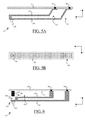
Figures 3A and 3B schematically show a MEMS probe according to an embodiment of the present invention; -
Figure 3C illustrates a method for verifying the integrity of the probes ofFigures 3A and 3B according to an embodiment of the present invention; -
Figure 4A and 4B illustrates how the probe ofFigures 3A and 3B may be connected to a substrate according to two embodiments of the present invention; -
Figure 5A and 5B schematically illustrates a MEMS probe according to a further embodiment of the present invention; -
Figure 6 schematically shows a MEMS probe according to a still further embodiment of the present invention; -
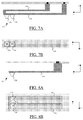
Figures 7A and 7B schematically illustrate a MEMS probe according to an embodiment of the present invention; -
Figures 8A and 8B schematically illustrate a MEMS probe according to an alternative embodiment of the present invention; -
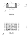
Figures 9A and 9B schematically illustrate a MEMS probe according to a still further alternative embodiment of the present invention, and -
Figures 10A and 10B schematically illustrate a MEMS probe according to a further embodiment of the present invention. - With reference to
Figure 1 , there is schematically illustrated a sectional view of a portion of atest apparatus 100 comprising aprobe card 105 adapted to electrically couple circuits integrated indice 102 of asemiconductor material wafer 110 to be tested. - The
wafer 110 is located on a chuck /hub 115 capable of being moved along the three orthogonal directions "x", "y" and "z" schematically shown in the figure; thechuck 115 may be further rotated and inclined. Once thesemiconductor wafer 110 is positioned on thechuck 115, the latter is moved in such a way to bring thewafer 110 to be tested in contact with theprobe card 105. - In the considered example, the
probe card 105 includes aPCB 125 connected to a substrate 130 (for example, formed by a semiconductor or ceramic material). Thesubstrate 130 supports a plurality of MEMS probes 135 adapted toelectrically contact pads 137 formed on thedice 102 of thewafer 110 to be tested. - The
PCB 125 comprises the circuits required for the communication between a tester (not illustrated in the figure) and thewafer 110 to be tested. For example, thePCB 125 comprises circuits for processing data/signals that control the whole operation of theprobe card 105, and that may operate under the control of a software stored in a memory unit (for example, one or more memories included in the PCB 125). - Although in the considered example the
probes 135 are supported by asubstrate 130, the concepts of the present invention are applicable to the case ofprobes 135 directly connected to thePCB 125. - Particular or "fiducial" marks 140 may be provided on the
PCB 125 or on thesubstrate 130 for allowing the correct alignment between theprobe card 105 and thewafer 110. - The
probes 135 are arranged on thesubstrate 130 in such a way each one of them results adapted to establish a relationship communication with arespective contact pad 137 of adie 102 of thewafer 110 to be tested. - The
Figure 2A is a prospect view illustrating the structure of aMEMS probe 135 according to an embodiment known in the art. Particularly, theprobe 135 comprises anelastic beam 210 of a conductor material (such as gold, silver, palladium, nickel, copper, manganese, tungsten, beryllium and corresponding alloys, or silicon) which extends substantially parallel to abottom surface 215 of thesubstrate 130. For example, making use of the conventions used inFigure 1 , theelastic beam 210 may substantially extends along the x direction. An end of theelastic beam 210 is connected to thesubstrate 130 through aconductive pillar 220 which substantially extends along the z direction. The other end of theelastic beam 210 is provided with a protrudingtip 230 adapted to electrically contact acontact pad 137 of thewafer 110 to be tested. Theprobe 135 may be possibly covered in part by at least one layer of conductor material in order to have proper electric and mechanic characteristics. Theprobe 135 is capable of exchanging test signals with thePCB 125 over thesubstrate 130 by means of a correspondingconductive track 240 which crosses thesubstrate 130. Particularly, a first end of suchconductive track 240 is connected to thepillar 220 of theprobe 135 by thebottom surface 215 of thesubstrate 130, while a second end is connected to thePCB 125 by atop surface 245 of thesubstrate 130 opposed to thebottom surface 215. - As already discussed above, a
probe 135 structured in this way has a single conductive path that starts from thetip 230, crosses theelastic beam 210, continues along thepillar 220 and reaches thePCB 130 through theconductive track 240. - In
Figure 2B it is illustrated a method normally used for verifying the integrity of theprobe 135. In order to consider theprobe 135 as usable in a test operation, the conductive path defined by the probe has to be characterized by an equivalent electric resistance that is sufficiently reduced. Indeed, the electric resistance increasing due to the presence of possible defects, breakings or structural deformations of theprobe 135 may be such to invalidate the correct transferring of the test signals from the circuits integrated in thewafer 110 to be tested to the tester and vice versa. - For this purpose, the
probe card 105 is typically positioned on a metallic plate, identified inFigure 2B with thereference 250. The metallic plate is electrically coupled with the end of theconductive track 240 on thetop surface 245 of thesubstrate 130 by means of a resistance measuring device, identified with thereference 260. - For example, the measuring
device 260 may include avoltage generator 265 adapted to generate a measuring voltage Vg having a predetermined value; the voltage difference applied between the metallic plate and the end of theconductive track 240 on thetop surface 245 by such generator generates a current Im flowing through the path formed by: metallic plate, probe's tip, elastic beam, pillar, conductive track and voltage generator included in the measuring device. Knowing the resistance of theconductive track 240, of themetallic plate 250 and the internal resistance of the measuringdevice 260, it is possible to determine the equivalent resistance of theprobe 135 by measuring the current Im by means of anamperometer 270. - As already mentioned in the introduction of the present document, positioning the
probe card 105 on themetallic plate 250 may be dangerous, since it is possible to damage thetip 230 of theprobe 135 in an irreversible way. - Although different methods for measuring the resistance of the
probes 135 are known, for example making use of measuring devices different than the measuringdevice 260, the conformation of the conductive path of theprobe 135 illustrated inFigure 2A always requires a "closure" of the circuit between theconductive track 240 and thetip 230 of theprobe 135. This requires that the tip 230 - i.e. the most fragile part of the probe 135 - is necessarily contacted in some way. - According to an embodiment of the present invention, such drawback is solved modifying the structure of the
probe 135 in such a way that it may be crossed by current during the integrity verifying without having to necessarily contacting thetip 230. As will be more clear in the following to the present description, this results to be possible by providing theprobe 135 with a conductive path which crosses all theprobe 135 and that can by "closed" between two points arranged by thesubstrate 130. - The
Figures 3A and 3B illustrate in detail the structure of theprobe 135 according to an embodiment of the present invention. Particularly,Figure 3A shows theprobe 135 according to a prospect view, while theFigure 3B according to a top view. - According said embodiment, the
probe 135 comprises a firstelastic beam 310 of a semiconductor material which substantially extends along the x direction, i.e. it is substantially parallel to thebottom surface 215 of thesubstrate 130. Anend 315 of such firstelastic beam 310 is connected to thesubstrate 130 by means of apillar 320 of semiconductor or conductor material which substantially extends along the z direction. The other end of the first elastic beam 310 - identified in figure with the reference 325 - is connected to thetip 230. Theprobe 135 comprises a secondelastic beam 330 positioned at an height (along the z axis) different than the firstelastic beam 310. For example, the secondelastic beam 330 may be in a position closer to thebottom surface 215 of thesubstrate 130 with respect to the firstelastic beam 310. Anend 340 of the secondelastic beam 330 is connected to theend 325 of the firstelastic beam 310 by means of a conductive material connection element, indicated in the figure with thereference 345. The other end of thesecond beam 330 - identified in the figure with the reference 350 - is connected to the
substrate 130 by means of a semiconductor orconductor material pillar 355 which substantially extends along the z direction. Theprobe 135 is capable of exchanging test signals with thePCB 125 by means of two conductive tracks which cross thesubstrate 130, identified with thereferences conductive track 360 is connected to thepillar 320 of the probe of thesubstrate 130, while a secondconductive track 365 is connected to thepillar 355. Both theconductive tracks substrate 130 until thetop surface 245. - Unlike the
probe 135 illustrated inFigure 2A , theprobe 135 ofFigures 3A and 3B has a conductive path that starts and ends on thetop surface 245 of thesubstrate 130. Particularly, such conductive path crosses theconductive track 365, reaches thepillar 355, carries on along theelastic beam 330, continues trough theconnection element 345 for reaching theelastic beam 310, carries on along thepillar 320 and reaches again thetop surface 245 through theconductive path 365. - Thanks to the peculiar structure of the
probe 135 illustrated in theFigures 3A and 3B , it is possible to measure the electric resistance of the conductive track - and, thus, to verify the effective integrity of the probe - in a easier and especially safer way, without having to contact thetip 230 in any way. - Particularly, as it is illustrated in
Figure 3C , according to an embodiment of the present invention it is sufficient to connect themeasuring device 260 between the firstconductive track 360 and the secondconductive track 365. In this way, the current Im generated by the measuringdevice 260 flows through the path formed by:conductive track 365,pillar 355, secondelastic beam 330,connection element 345, firstelastic beam 310,pillar 320,conductive track 360 andvoltage generator 265 within the measuringdevice 260; naturally, the path may be crossed in the opposite direction as well. - In case the MEMS probe is at least partially comprised into / surrounded by the sacrificial oxide (or any other equivalent sacrificial insulating material employed in a MEMS technology process) it is possible to perform the electrical test. Obviously the sacrificial oxide will be removed to use the probe.
- It has to be noted that with this solution it may not be possible to verify with electrical measurements the correct operation of the
tip 230 of theprobe 135, sincesuch tip 230 is not crossed by the current Im. However, in order to verify the integrity of thetip 230 it is sufficient to carry out an optical inspection, for assessing if the shape of the tip respects predetermined specifications or not. - The
probe 135 may be connected to thePCB 125 with ease by short-circuiting the firstconductive track 360 and the secondconductive track 365 to a corresponding contact on thePCB 125. - Alternatively, according to an embodiment of the present invention illustrated in
Figure 4A , it is possible to provide a further substrate - identified with the reference 410- including a singleconductive track 420, and connecting an end of such conductive track to the firstconductive track 360 by means of afirst contact terminal 430 and to the secondconductive track 365 by means of asecond contact terminal 440. In this way, the test signals are capable of reaching thetip 230 of theprobe 135 even if one of the twocontact terminals probe 135 due to the passing of time. This embodiment is particularly but not exclusively useful for high current applications. - According to a further embodiment of the present invention illustrated in
Figure 4B , thesubstrate 410 may be provided with two distinct conductive tracks, each one adapted to be contacted to a respective conductive track in thesubstrate 130. Particularly, thesubstrate 410 includes aconductive track 450 connected to the firstconductive track 360 by means of thefirst terminal 430 and a secondconductive track 460 connected to the secondconductive track 365 by means of thesecond terminal 440. Then, theconductive tracks PCB 125 or external systems connected to thePCB 125. - According to an alternative embodiment of the present invention, the
probe 135 may be connected to thesubstrate 130 by directly connecting the beams to thesubstrate 130. For example, in theprobe 135 illustrated in theFigures 5A and 5B , the firstelastic beam 310 and the secondelastic beam 330 are shaped in such a way to exhibit folds with a component in the z direction at theends end 315 of the firstelastic beam 310 to the firstconductive track 360 in thesubstrate 130 and theend 350 of the secondelastic beam 330 to the secondconductive track 365, the probe may receive/transmit test signals from/to the PCB 125 (and, thus, from/to the tester) without any pillar. - According to a further embodiment of the present invention, illustrated in
Figure 6 , it is possible to provide anhousing 610 in the end of theprobe 135 coupled with thetip 230, for example by connecting theconnection element 345 between theend 340 of the secondelastic beam 330 and an intermediate point (but close to the end 325) of the firstelastic beam 310. In this way, by connecting to thebottom surface 215 of the substrate 130 a protruding blockingelement 615 adapted to cooperate with thehousing 610 when the probe is subjected to a deformation - whose direction is indicated with the reference 620 - generated in response to possible excessive pressures of thewafer 110 to be tested against theprobe card 105, it is possible to safeguard the integrity of theprobe 135. - Being provided with two
distinct beams probe 135 according to one of the embodiments of the present invention may conduct currents having relatively high values. In this way, it is possible to increment the maximum current a MEMS probe may conduct, which, as it is well known, is lower than the maximum current a probe of the cantilever type or fabricated by means of vertical technologies is able to conduct.. On this regard, as illustrated in theFigures 7A and 7B , the probe may be provided with at least one additional tip, identified with thereference 710. It has to be noted that in case of high currents, thecontact pads 137 formed on thedice 102 of thewafer 110 to be tested which will be contacted by theprobes 135, as well as the probe tip surfaces, will have an higher size. In this case, the bonds on the size of theprobes 135 are less restrictive, and thus it is possible to simplify their structure. Particularly, in theprobe 135 according to an embodiment of the present invention illustrated in theFigures 8A and 8B , the firstelastic beam 310 and the secondelastic beam 330 are arranged side to side on a same plane at a same distance (according the z direction) from thebottom surface 215 of thesubstrate 130. - According to a further embodiment of the present invention illustrated in the
Figures 9A and 9B , it is possible to provide a single beam - identified with the reference 910 - connected to thesubstrate 130 by means of twopillars beam 910; one ormore tips 230 may be positioned on the median portion of thebeam 910. - The double-beam structure according to one embodiment of the present invention may be advantageously employed for implementing a termocouple or a temperature sensor adapted for example to efficiently measure the temperature of the devices integrated in the
dice 102 of thewafer 110 to be tested by directly using theprobe card 105. Theprobe 135 illustrated in theFigures 8A and 8B may be easily employed as a termocouple, realizing for example the firstelastic beam 310 with a material different than that of the secondelastic beam 330 to the purpose of exploiting the Seebeck effect for measuring a temperature value based on a corresponding voltage difference developing across the firstelastic beam 310 and the secondelastic beam 330. Moreover, by realizing the firstelastic beam 310 with a material different than that of the secondelastic beam 330, theprobe 135 may be employed to set a specific temperature in a certain area of a device integrated in thedice 102 of thewafer 110 or to transfer heat from such device to theprobe card 105 through the probe (e.g., so as to chill the device) by properly biasing the probe and then exploiting the Peltier effect. - According to a further embodiment of the present invention, it is possible to exploit the
probe 135 for efficiently measuring the pressure exerted by thewafer 110 against theprobe card 105 during the test operations. Particularly, making reference to theFigures 10A and 10B , thebeams elastic probe 135 may be advantageously employed for forming the bottom plate of a capacitor; the top plate of such capacitor - identified in figure with the reference 1010 - may be implemented by means of a metallic layer formed on thebottom surface 215 of thesubstrate 130 properly connected to aconductive track 1020 formed in thesubstrate 130 itself. During the test operations, thebeams wafer 110 against theprobe card 105. The effect of such deformation changes the value of the capacitor's capacitance; particularly, the value of the capacitance increases when thebeams probe 135 come close to thebottom surface 215 of thesubstrate 130. As a consequence, by measuring the capacity of the capacitor using a proper capacitance measuring device (not illustrated in figure) it is possible to obtain an information on the actual pressure exerted by thewafer 110. In order to improve the reliability of the measure, it is convenient to increase the width of thebeams 310 and 330 (along the y direction), and thus increasing the capacitive coupling between the plates. For example, thebeams Figure 10B have a tapered shape, whose width (along the y direction) increases as approaching to the pillars connected to thesubstrate 130. According to an alternative embodiment of the present invention the bottom plate of the capacitor may be implemented using a probe with a singular beam having a higher width (along the y direction). Advantageously, this structure may be employed for increasing or reducing the pressure exerted by theprobe 135 on thewafer 110 by properly biasing the two plates of the capacitor by means of a proper biasing device (not shown in the figure). - Regarding the production of the various probes proposed according to the embodiments of the present invention, it is sufficient to exploit any one among the MEMS manufacturing lithographic process known to the skilled in the art, starting for example from a sacrificial substrate formed for example by a semiconductor material wafer, and then soldering the probes to the final substrate, or using the semiconductor material wafer as the final substrate.
- Naturally, in order to satisfy local and specific requirements, a person skilled in the art may apply to the solution described above many modifications and alterations. Particularly, although the present invention has been described with a certain degree of particularity with reference to preferred embodiment(s) thereof, it should be understood that various omissions, substitutions and changes in the form and details as well as other embodiments are possible; moreover, it is expressly intended that specific elements and/or method steps described in connection with any disclosed embodiment of the invention may be incorporated in any other embodiment as a general matter of design choice.
- Particularly, the concepts of the present invention may be applied to any type of MEMS probe known to the skilled technician, but that has not been described in detail.
- For example, the
probes 135 according to any one among the embodiments of the present invention may be arranged in more than one level, aligned along a same axis with respect the plane (x, y) - or with a little deviation-, includebeams tips 320 having different shape and size, in such a way to be capable of better optimize the electric contact with thecontact pads 137 formed on thedice 102 of thewafer 110 to be tested. - Moreover, the proposed double-beam structure may be advantageously exploited for forming an electric link with protruding contact regions ("bumps") formed on the
wafer 110, for example arranging a plurality of tips on eachbeam
Claims (13)
- A microelectromechanical probe (135) adapted to contact a corresponding terminal of an integrated circuit, integrated on at least one chip (102) of a semiconductor material wafer (110) during a test phase of the wafer, said probe including:a support structure (310, 330, 355, 325, 345) comprising a first access terminal and a second access terminal, said support structure defining a conductive path between said first access terminal and said second access terminal;a probe region (230) connected to the support structure, said probe region comprising at least one conductive tip adapted to contact the corresponding terminal of the integrated circuit during the test phase for:characterized in that- providing at least one test signal received from the first access terminal and the second access terminal to the integrated circuit through at least one portion of the conductive path, and/or- providing at least one test signal generated by the integrated circuit to at least one between the first access terminal and the second access terminal trough at least one portion of the conductive path,
said probe region is arranged on the conductive path of the support structure between said first access terminal and said second access terminal. - The probe according to claim 1, wherein the probe is adapted to be connected to a first surface of a substrate element (130) comprising a first conductive track (360) and a second conductive track (365), said first access terminal and said second access terminal being adapted to be connected to the first conductive track and to the second conductive track, respectively, for providing/receiving the at least one test signal.
- The probe according to claim 2, wherein said support structure comprises at least one beam element (310, 330; 910) that extends along a direction substantially parallel to the first surface of the substrate element, a portion of said conductive path being defined by said at least one beam element.
- The probe according to claim 3, wherein the probe region is connected to the at least one beam element.
- The probe according to claim 3 or claim 4, wherein:- said at least one beam element comprises a first beam element (310) and a second beam element (330);- the first beam element is connected to the first conductive track by means of a first pillar element (320) and the second beam element is connected to the second conductive track by means of a second pillar element (355), a further portion of said conductive path being defined by said first and second pillar elements;- the first beam element is connected to the second beam element by means of a link element (345), a still further portion of said conductive path being defined by said link element.
- The probe according to claim 5, wherein:- the first pillar element and the second pillar element are connected to a first end of the first beam element and to a first end of the second beam element, respectively;- the link element is connected to a second end of the first beam element and to a second end of the second beam element; and- the probe region is connected to the second end of at least one between the first and the second beam elements.
- A probe card (105) adapted to be used for testing at least one integrated circuit, integrated on at least one corresponding chip (102) of a semiconductor material wafer (110), the probe card comprising a board (125) adapted to the coupling with a test apparatus, and a plurality of probes (135) coupled with said board by means of a substrate element (130),
characterized in that
said probes comprise at least one probe according to any one among the preceding claims. - A test apparatus (100) for testing at least one integrated circuit, integrated on at least one chip (102) belonging to a semiconductor material wafer (110), the apparatus comprising:a probe card (105) adapted to behave as a communication interface between a tester and the chip of the semiconductor material wafer,characterized in that
the probe card is constructed according to claim 7. - A method for verifying the integrity of a microelectromechanical probe (135) adapted to contact a corresponding terminal of an integrated circuit, integrated on at least one chip (102) of a semiconductor material wafer (110) during a test phase of the wafer, said probe including:a support structure (310, 330, 355, 325, 345) comprising a first access terminal and a second access terminal, said support structure defining a conductive path between said first access terminal and said second access terminal;a probe region (230) connected to the support structure, said probe region comprising at least one conductive tip adapted to contact the corresponding terminal of the integrated circuit during the test phase for:- providing at least one test signal received from the first access terminal and the second access terminal to the integrated circuit through at least one portion of the conductive path, and/or- providing at least one test signal generated by the integrated circuit to at least one between the first access terminal and the second access terminal trough at least one portion of the conductive path, said probe region is arranged on the conductive path of the support structure between said first access terminal and said second access terminal, said method for verifying including:- accessing the first and the second input terminals with a measuring device (260);- stimulating the probe with said measuring device in such a way the conductive path is crossed by a measuring current (Im), and- assessing the integrity of the probe based on the measuring current.
- Use of a probe (135) adapted to contact a corresponding terminal of an integrated circuit, integrated on at least one chip (102) of a semiconductor material wafer (110), as a device for measuring the temperature of the terminal,
characterized in that- said probe is the probe of claim 5 or 6; and- the first beam element (310) is made of a conductive material of a first type, and the second beam element (330) is made of a conductive material of a second type different from the first one, said use comprising:- measuring a voltage difference between the first beam element and the second beam element, and- measuring the temperature of said terminal based on said voltage difference. - Use of a probe (135) adapted to contact a corresponding terminal of an integrated circuit, integrated on at least one chip (102) of a semiconductor material wafer (110), as a device for exchanging heat with the terminal,
characterized in that- said probe is the probe of claim 5 or 6; and- the first beam element (310) is made of a conductive material of a first type, and the second beam element (330) is made of a conductive material of a second type different from the first one, said use comprising:- biasing the probe with a biasing voltage, and- exchanging heat with the terminal based on a corresponding voltage difference developing between the first beam element and the second beam element because of said biasing voltage. - Use of a probe card (105) adapted to be used for testing at least one integrated circuit, integrated on at least one corresponding chip (102) of a semiconductor material wafer (110), for measuring the pressure exerted by the semiconductor material wafer against the probe card, the probe card comprising a board (125) adapted to the coupling to a test apparatus, and a plurality of probes (135) coupled with said board by means of a substrate element (130),
characterized in that- said probes include at least one probe according to any one among claims 1-6; and- the substrate element includes a metallic layer (1010) in correspondence of the at least one probe, said metallic layer and said at least one probe defining the plates of a capacitor;, said use comprising:- measuring the capacity of said capacitor, and- measuring the pressure exerted by the semiconductor material wafer against the probe card based on the measured capacity. - Use of a probe card (105) adapted to be used for testing at least one integrated circuit, integrated on at least one corresponding chip (102) of a semiconductor material wafer (110), for controlling the pressure exerted by the semiconductor material wafer against the probe card, the probe card comprising a board (125) adapted to the coupling to a test apparatus, and a plurality of probes (135) coupled with said board by means of a substrate element (130),
characterized in that- said probes include at least one probe according to any one among claims 1-6; and- the substrate element includes a metallic layer (1010) in correspondence of the at least one probe, said metallic layer and said at least one probe defining the plates of a capacitor, said use comprising:- biasing said capacitor with a biasing voltage, and- controlling the pressure exerted by the semiconductor material wafer against the probe card based on such biasing voltage.
Applications Claiming Priority (1)
| Application Number | Priority Date | Filing Date | Title |
|---|---|---|---|
| ITMI20082347 | 2008-12-30 |
Publications (1)
| Publication Number | Publication Date |
|---|---|
| EP2204656A1 true EP2204656A1 (en) | 2010-07-07 |
Family
ID=41258346
Family Applications (1)
| Application Number | Title | Priority Date | Filing Date |
|---|---|---|---|
| EP09181012A Withdrawn EP2204656A1 (en) | 2008-12-30 | 2009-12-30 | Improved MEMS probe for probe cards for integrated circuits |
Country Status (2)
| Country | Link |
|---|---|
| US (1) | US8441272B2 (en) |
| EP (1) | EP2204656A1 (en) |
Cited By (2)
| Publication number | Priority date | Publication date | Assignee | Title |
|---|---|---|---|---|
| WO2012143797A1 (en) * | 2011-04-21 | 2012-10-26 | Freescale Semiconductor, Inc. | System and method to test a semiconductor power switch |
| WO2022033300A1 (en) * | 2020-08-14 | 2022-02-17 | 强一半导体(苏州)有限公司 | Mems probe card |
Families Citing this family (7)
| Publication number | Priority date | Publication date | Assignee | Title |
|---|---|---|---|---|
| ITMI20072399A1 (en) * | 2007-12-20 | 2009-06-21 | St Microelectronics Srl | PROBE BOARD IMPROVED TO TEST INTEGRATED CIRCUITS |
| JP6407672B2 (en) * | 2014-11-18 | 2018-10-17 | ルネサスエレクトロニクス株式会社 | Manufacturing method of semiconductor device |
| CN107402319A (en) * | 2016-05-19 | 2017-11-28 | 苏州明皜传感科技有限公司 | Measure the probe card of micro- electric capacity |
| KR102675691B1 (en) * | 2017-11-15 | 2024-06-14 | 카프레스 에이/에스 | A probe for testing an electrical property of a test sample |
| US11740279B2 (en) * | 2020-04-24 | 2023-08-29 | Kla Corporation | Measuring temperature-modulated properties of a test sample |
| US12019097B2 (en) * | 2021-08-30 | 2024-06-25 | Taiwan Semiconductor Manufacturing Company, Ltd. | Method for forming probe head structure |
| US12529724B2 (en) * | 2023-05-19 | 2026-01-20 | Fei Company | Capacitance-based detection of probe contact |
Citations (11)
| Publication number | Priority date | Publication date | Assignee | Title |
|---|---|---|---|---|
| US4056777A (en) * | 1974-08-14 | 1977-11-01 | Electroglas, Inc. | Microcircuit test device with multi-axes probe control |
| US5475318A (en) * | 1993-10-29 | 1995-12-12 | Robert B. Marcus | Microprobe |
| EP0752587A2 (en) * | 1995-07-07 | 1997-01-08 | Hewlett-Packard Company | Electrical connection structure |
| DE19944980A1 (en) * | 1998-09-21 | 2000-03-23 | Advantest Corp | Encased electrical connection for a connecting structure used for testing, e.g., semiconductor wafer has a holding structure arranged between an elastomeric element and PCB substrate |
| US6181144B1 (en) * | 1998-02-25 | 2001-01-30 | Micron Technology, Inc. | Semiconductor probe card having resistance measuring circuitry and method fabrication |
| WO2001084166A1 (en) * | 2000-05-02 | 2001-11-08 | Thomas Di Stefano | Compliant probe apparatus |
| US20020005728A1 (en) * | 1999-04-15 | 2002-01-17 | Gordon M. Babson | Micro probe and method of fabricating same |
| US20020113609A1 (en) * | 1999-01-19 | 2002-08-22 | Hiroshi Noda | Probe stylus |
| US20040142583A1 (en) * | 1998-12-02 | 2004-07-22 | Formfactor, Inc. | Spring interconnect structures |
| KR20050067758A (en) * | 2003-12-29 | 2005-07-05 | 동부아남반도체 주식회사 | Probe card |
| US20070018664A1 (en) * | 2005-07-25 | 2007-01-25 | Samsung Electronics Co., Ltd. | Probe card, test apparatus having the probe card, and test method using the test apparatus |
Family Cites Families (10)
| Publication number | Priority date | Publication date | Assignee | Title |
|---|---|---|---|---|
| US7063541B2 (en) * | 1997-03-17 | 2006-06-20 | Formfactor, Inc. | Composite microelectronic spring structure and method for making same |
| US6811406B2 (en) * | 2001-04-12 | 2004-11-02 | Formfactor, Inc. | Microelectronic spring with additional protruding member |
| JP3574444B2 (en) * | 2002-08-27 | 2004-10-06 | 沖電気工業株式会社 | Method of measuring contact resistance of probe and method of testing semiconductor device |
| US20060038576A1 (en) * | 2004-08-19 | 2006-02-23 | Pooya Tadayon | Sort interface unit having probe capacitors |
| KR100626570B1 (en) * | 2004-12-24 | 2006-09-25 | 주식회사 파이컴 | Probe card manufacturing method including probe for detection and probe card, probe card inspection system |
| US7245135B2 (en) * | 2005-08-01 | 2007-07-17 | Touchdown Technologies, Inc. | Post and tip design for a probe contact |
| US7579856B2 (en) * | 2006-04-21 | 2009-08-25 | Formfactor, Inc. | Probe structures with physically suspended electronic components |
| US7952375B2 (en) * | 2006-06-06 | 2011-05-31 | Formfactor, Inc. | AC coupled parameteric test probe |
| DE102007013063A1 (en) * | 2007-03-19 | 2008-10-09 | Qimonda Ag | Apparatus and method for electrical contacting of semiconductor devices for test purposes |
| US7898266B2 (en) * | 2008-06-04 | 2011-03-01 | Seagate Technology Llc | Probe with electrostatic actuation and capacitive sensor |
-
2009
- 2009-12-29 US US12/649,109 patent/US8441272B2/en active Active
- 2009-12-30 EP EP09181012A patent/EP2204656A1/en not_active Withdrawn
Patent Citations (11)
| Publication number | Priority date | Publication date | Assignee | Title |
|---|---|---|---|---|
| US4056777A (en) * | 1974-08-14 | 1977-11-01 | Electroglas, Inc. | Microcircuit test device with multi-axes probe control |
| US5475318A (en) * | 1993-10-29 | 1995-12-12 | Robert B. Marcus | Microprobe |
| EP0752587A2 (en) * | 1995-07-07 | 1997-01-08 | Hewlett-Packard Company | Electrical connection structure |
| US6181144B1 (en) * | 1998-02-25 | 2001-01-30 | Micron Technology, Inc. | Semiconductor probe card having resistance measuring circuitry and method fabrication |
| DE19944980A1 (en) * | 1998-09-21 | 2000-03-23 | Advantest Corp | Encased electrical connection for a connecting structure used for testing, e.g., semiconductor wafer has a holding structure arranged between an elastomeric element and PCB substrate |
| US20040142583A1 (en) * | 1998-12-02 | 2004-07-22 | Formfactor, Inc. | Spring interconnect structures |
| US20020113609A1 (en) * | 1999-01-19 | 2002-08-22 | Hiroshi Noda | Probe stylus |
| US20020005728A1 (en) * | 1999-04-15 | 2002-01-17 | Gordon M. Babson | Micro probe and method of fabricating same |
| WO2001084166A1 (en) * | 2000-05-02 | 2001-11-08 | Thomas Di Stefano | Compliant probe apparatus |
| KR20050067758A (en) * | 2003-12-29 | 2005-07-05 | 동부아남반도체 주식회사 | Probe card |
| US20070018664A1 (en) * | 2005-07-25 | 2007-01-25 | Samsung Electronics Co., Ltd. | Probe card, test apparatus having the probe card, and test method using the test apparatus |
Non-Patent Citations (1)
| Title |
|---|
| DATABASE WPI Week 200650, Derwent World Patents Index; AN 2006-486445 * |
Cited By (3)
| Publication number | Priority date | Publication date | Assignee | Title |
|---|---|---|---|---|
| WO2012143797A1 (en) * | 2011-04-21 | 2012-10-26 | Freescale Semiconductor, Inc. | System and method to test a semiconductor power switch |
| WO2022033300A1 (en) * | 2020-08-14 | 2022-02-17 | 强一半导体(苏州)有限公司 | Mems probe card |
| US12222369B2 (en) | 2020-08-14 | 2025-02-11 | Maxone Semiconductor Co., Ltd. | MEMS probe card |
Also Published As
| Publication number | Publication date |
|---|---|
| US8441272B2 (en) | 2013-05-14 |
| US20100164526A1 (en) | 2010-07-01 |
Similar Documents
| Publication | Publication Date | Title |
|---|---|---|
| US8441272B2 (en) | MEMS probe for probe cards for integrated circuits | |
| JP5486866B2 (en) | Manufacturing method of semiconductor device | |
| CN101946182B (en) | Improved probe card for testing integrated circuits | |
| KR20050041885A (en) | Fabrication method of semiconductor integrated circuit device | |
| JP2001056345A (en) | Probing card and method of manufacturing the same | |
| CN101154609B (en) | Bump testing unit, device and testing method | |
| KR20020026852A (en) | Fabrication method of semiconductor integrated circuit device and its testing apparatus | |
| CN110907788B (en) | Probe card inspection wafer and probe card inspection system | |
| KR100787829B1 (en) | Probe card test device and test method | |
| KR100712561B1 (en) | Wafer type probe card, manufacturing method thereof and semiconductor inspection device provided with wafer type probe card | |
| JP5854879B2 (en) | Non-contact type probe card | |
| US8786303B2 (en) | Semiconductor device having a plurality of pads | |
| US12449479B2 (en) | Testing system for integrated circuit device, and signal source and power supplying apparatus | |
| JP2005315775A (en) | Four-terminal inspection method and single-terminal inspection jig using a single-sided moving probe | |
| US12094789B2 (en) | Analog sense points for measuring circuit die | |
| KR20090075515A (en) | Probe Cards and Test Equipment Including the Same | |
| US20080061812A1 (en) | Component-attach test vehicle | |
| JP4962929B2 (en) | PROBER DEVICE AND PROBE ASSEMBLY USED FOR THE SAME | |
| TWI881360B (en) | Probe cadr structure for high frequency test and testing method thereof | |
| JP2008205282A (en) | Probe card | |
| KR200221077Y1 (en) | Conductive polymer probe card | |
| JPH0720150A (en) | Probe card and test apparatus using the same | |
| JPH04236440A (en) | Semiconductor test apparatus | |
| KR20100067861A (en) | Probe card and manufacturing methods thereof | |
| JP2007012709A (en) | Semiconductor inspection apparatus and semiconductor device inspection method |
Legal Events
| Date | Code | Title | Description |
|---|---|---|---|
| PUAI | Public reference made under article 153(3) epc to a published international application that has entered the european phase |
Free format text: ORIGINAL CODE: 0009012 |
|
| AK | Designated contracting states |
Kind code of ref document: A1 Designated state(s): AT BE BG CH CY CZ DE DK EE ES FI FR GB GR HR HU IE IS IT LI LT LU LV MC MK MT NL NO PL PT RO SE SI SK SM TR |
|
| AX | Request for extension of the european patent |
Extension state: AL BA RS |
|
| 17P | Request for examination filed |
Effective date: 20101215 |
|
| 17Q | First examination report despatched |
Effective date: 20110110 |
|
| RAP1 | Party data changed (applicant data changed or rights of an application transferred) |
Owner name: STMICROELECTRONICS SRL |
|
| STAA | Information on the status of an ep patent application or granted ep patent |
Free format text: STATUS: THE APPLICATION IS DEEMED TO BE WITHDRAWN |
|
| 18D | Application deemed to be withdrawn |
Effective date: 20150701 |