EP2204474A1 - Method for fabricating multi-component nanowires - Google Patents
Method for fabricating multi-component nanowires Download PDFInfo
- Publication number
- EP2204474A1 EP2204474A1 EP09011927A EP09011927A EP2204474A1 EP 2204474 A1 EP2204474 A1 EP 2204474A1 EP 09011927 A EP09011927 A EP 09011927A EP 09011927 A EP09011927 A EP 09011927A EP 2204474 A1 EP2204474 A1 EP 2204474A1
- Authority
- EP
- European Patent Office
- Prior art keywords
- nanowires
- component
- aluminum oxide
- anodized aluminum
- solution
- Prior art date
- Legal status (The legal status is an assumption and is not a legal conclusion. Google has not performed a legal analysis and makes no representation as to the accuracy of the status listed.)
- Granted
Links
Images






Classifications
-
- C—CHEMISTRY; METALLURGY
- C30—CRYSTAL GROWTH
- C30B—SINGLE-CRYSTAL GROWTH; UNIDIRECTIONAL SOLIDIFICATION OF EUTECTIC MATERIAL OR UNIDIRECTIONAL DEMIXING OF EUTECTOID MATERIAL; REFINING BY ZONE-MELTING OF MATERIAL; PRODUCTION OF A HOMOGENEOUS POLYCRYSTALLINE MATERIAL WITH DEFINED STRUCTURE; SINGLE CRYSTALS OR HOMOGENEOUS POLYCRYSTALLINE MATERIAL WITH DEFINED STRUCTURE; AFTER-TREATMENT OF SINGLE CRYSTALS OR A HOMOGENEOUS POLYCRYSTALLINE MATERIAL WITH DEFINED STRUCTURE; APPARATUS THEREFOR
- C30B7/00—Single-crystal growth from solutions using solvents which are liquid at normal temperature, e.g. aqueous solutions
- C30B7/12—Single-crystal growth from solutions using solvents which are liquid at normal temperature, e.g. aqueous solutions by electrolysis
-
- B—PERFORMING OPERATIONS; TRANSPORTING
- B82—NANOTECHNOLOGY
- B82B—NANOSTRUCTURES FORMED BY MANIPULATION OF INDIVIDUAL ATOMS, MOLECULES, OR LIMITED COLLECTIONS OF ATOMS OR MOLECULES AS DISCRETE UNITS; MANUFACTURE OR TREATMENT THEREOF
- B82B3/00—Manufacture or treatment of nanostructures by manipulation of individual atoms or molecules, or limited collections of atoms or molecules as discrete units
-
- C—CHEMISTRY; METALLURGY
- C25—ELECTROLYTIC OR ELECTROPHORETIC PROCESSES; APPARATUS THEREFOR
- C25D—PROCESSES FOR THE ELECTROLYTIC OR ELECTROPHORETIC PRODUCTION OF COATINGS; ELECTROFORMING; APPARATUS THEREFOR
- C25D1/00—Electroforming
- C25D1/04—Wires; Strips; Foils
-
- C—CHEMISTRY; METALLURGY
- C30—CRYSTAL GROWTH
- C30B—SINGLE-CRYSTAL GROWTH; UNIDIRECTIONAL SOLIDIFICATION OF EUTECTIC MATERIAL OR UNIDIRECTIONAL DEMIXING OF EUTECTOID MATERIAL; REFINING BY ZONE-MELTING OF MATERIAL; PRODUCTION OF A HOMOGENEOUS POLYCRYSTALLINE MATERIAL WITH DEFINED STRUCTURE; SINGLE CRYSTALS OR HOMOGENEOUS POLYCRYSTALLINE MATERIAL WITH DEFINED STRUCTURE; AFTER-TREATMENT OF SINGLE CRYSTALS OR A HOMOGENEOUS POLYCRYSTALLINE MATERIAL WITH DEFINED STRUCTURE; APPARATUS THEREFOR
- C30B29/00—Single crystals or homogeneous polycrystalline material with defined structure characterised by the material or by their shape
- C30B29/10—Inorganic compounds or compositions
- C30B29/46—Sulfur-, selenium- or tellurium-containing compounds
-
- C—CHEMISTRY; METALLURGY
- C30—CRYSTAL GROWTH
- C30B—SINGLE-CRYSTAL GROWTH; UNIDIRECTIONAL SOLIDIFICATION OF EUTECTIC MATERIAL OR UNIDIRECTIONAL DEMIXING OF EUTECTOID MATERIAL; REFINING BY ZONE-MELTING OF MATERIAL; PRODUCTION OF A HOMOGENEOUS POLYCRYSTALLINE MATERIAL WITH DEFINED STRUCTURE; SINGLE CRYSTALS OR HOMOGENEOUS POLYCRYSTALLINE MATERIAL WITH DEFINED STRUCTURE; AFTER-TREATMENT OF SINGLE CRYSTALS OR A HOMOGENEOUS POLYCRYSTALLINE MATERIAL WITH DEFINED STRUCTURE; APPARATUS THEREFOR
- C30B29/00—Single crystals or homogeneous polycrystalline material with defined structure characterised by the material or by their shape
- C30B29/60—Single crystals or homogeneous polycrystalline material with defined structure characterised by the material or by their shape characterised by shape
-
- B—PERFORMING OPERATIONS; TRANSPORTING
- B82—NANOTECHNOLOGY
- B82Y—SPECIFIC USES OR APPLICATIONS OF NANOSTRUCTURES; MEASUREMENT OR ANALYSIS OF NANOSTRUCTURES; MANUFACTURE OR TREATMENT OF NANOSTRUCTURES
- B82Y40/00—Manufacture or treatment of nanostructures
Definitions
- the present invention relates to a method for fabricating nanowires. More particularly, the present invention relates to a method for fabricating multi-component nanowires used to implement a nanowire-based memory device by an electroplating process using a multi-component solution.
- PRAM phase change random access memory
- ReRAM resistive random access memory
- DRAM dynamic random access memory
- the PRAM basically operates based on a different principle from that of a general semiconductor memory, and writes data using a phenomenon that the crystalline state of phase change materials based on chalcogenide compounds is changed by electrical switching.
- nanowires have been suggested as an alternative for a thin film as a memory layer in the PRAM.
- VLS vapor-liquid-solid
- CVD chemical vapor deposition
- PVD physical vapor deposition
- these conventional methods has a problem that the fabrication cost is high because the price of equipment used to fabricate nanowires is high or the process takes a long time and is complicated. That is, the conventional methods have been carried out usually by sputtering, E-beam evaporation or plasma enhanced chemical vapor deposition (PECVD), but have a problem that the fabrication cost is high and the fabrication process is complicated because high-priced equipment is used and the fabrication is performed in high temperature and vacuum.
- PECVD plasma enhanced chemical vapor deposition
- an object of the present invention to provide a method for fabricating multi-component nanowires, which makes the fabrication process easier and offers low fabrication cost by enabling it to fabricate multi-component nanowires in a nanotemplate having a plurality of pores by an electroplating process with the use of a multi-component solution.
- a method for fabricating multi-component nanowires including the steps of: (a) preparing an anodized aluminum oxide nanotemplate having a plurality of pores; (b) forming an electrode layer on one surface of the anodized aluminum oxide nanotemplate; (c) injecting the anodized aluminum oxide nanotemplate in a predetermined multi-component solution and then growing multi-component nanowires through the pores of the anodized aluminum oxide nanotemplate by an electroplating process in which the anodized aluminum oxide nanotemplate is used as a cathode; and (d) removing the anodized aluminum oxide nanotemplate.
- the diameter of the pores can be several tens to several hundreds nanometers.
- the electrode layer can comprise gold (Au).
- the multi-component solution is an Ag-Se solution
- Ag-Se nanowires can grow.
- the Ag-Se solution can include Ag and Se as precursors and nitric acid and ethylglycerol as solvents.
- the multi-component solution is a Ge-Sb-Te solution
- Ge-Sb-Te nanowires can grow.
- the Ge-Sb-Te solution can include GeO 2 , SbO 2 , and TeO 2 as precursors and hydrochloric acid and ethylglycerol as solvents.
- a platinum electrode can be used as an anode.
- a composition ratio of the multi-component nanowires can be determined depending on the change of at least one of a mixing ratio of precursors in the multi-component solution and a current density applied during the electroplating process.
- the anodized aluminum oxide nanotemplate can be removed with a NaOH solution.
- multi-component nanowires fabricated by the method disclosed above.
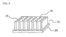
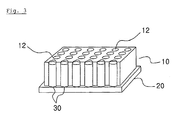
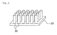
- Figs. 1 to 4 show the configuration of a method for fabricating multi-component nanowires in accordance with one embodiment of the present invention.
- an anodized aluminum oxide nanotemplate 10 is prepared.
- the anodized aluminum oxide nanotemplate 10 having a plurality of pores 12 formed thereon can be fabricated as follows.
- an aluminum having a purity of 99.999% is electrochemically etched to planarize a surface thereof, and then the aluminum is anodized in oxalic acid at a voltage of 40 V and a temperature of 4°C.
- the anodization When the anodization is carried out once, the uniformity of the pores 12 is poor, and therefore it is preferable to carry out the anodization twice in order to improve the uniformity of the pores 12.
- a firstly-formed anodized aluminum oxide layer is removed with chromic acid at a temperature of 65°C.
- the second anodization is carried out under the same condition as the first anodization.
- the aluminum is removed with a silver nitrate aqueous solution in order to leave only an anodized aluminum oxide layer formed by carrying out anodization twice.
- the pores 12 are expanded by using a phosphoric acid aqueous solution, thereby improving the uniformity of the pores 12 of the anodized aluminum oxide nanotemplate 10.
- the preparation of the anodized aluminum oxide nanotemplate 10 having the plurality of the pores 12 is completed (see Fig. 1 ).
- the diameter of the pores 12 formed on the anodized aluminum oxide nanotemplate 10 is preferably several tens to several hundreds nanometers (nm).
- an electrode layer 20 is formed on one surface of the anodized aluminum oxide nanotemplate 10.
- the electrode layer 20 is formed at a thickness of 300 to 400 nm by E-beam evaporation process on one surface of the anodized aluminum oxide nanotemplate 10 after completion of the formation of the anodized aluminum oxide nanotemplate 10.
- the material of the electrode layer 20 may comprise gold (Au).
- multi-component nanowires 30 are grown through the pores 12 of the anodized aluminum oxide nanotemplate 10 by using an electroplating process.
- the anodized aluminum oxide nanotemplate 10 having the plurality of pores 12 is injected in a multi-component solution, and then the electroplating process is carried out by using the anodized aluminum oxide nanotemplate 10 as a cathode.
- the multi-component solution used at this time may be an Ag-Se or Ge-Sb-Te solution for growing Ag-Se nanowires or Ge-Sb-Te nanowires that constitute the memory layer of the PRAM.
- a platinum electrode may be used as an opposite electrode of the anodized aluminum oxide nanotemplate 10 which is used as the cathode, i.e., an anode.
- the purity of the platinum is preferably 99.99%.
- the precursors may include Ag and Se and the solvents may include nitric acid and ethylglycerol.
- the solvents may include nitric acid and ethylglycerol.
- 0.1 mol of Ag, 0.05 mol of Se, 10 ml of nitric acid, and 100 ml of ethylglycerol were used.
- the precursors may include GeO 2 , SbO 2 , and TeO 2 and the solvents may include hydrochloric acid and ethylglycerol.
- the solvents may include hydrochloric acid and ethylglycerol.
- a composition ratio of the multi-component nanowires can be determined depending on the change of at least one of a mixing ratio of the precursors in a multi-component solution and an applied current density.
- the current density is preferably 2 mA/cm 2
- the current density is preferably 1 mA/cm 2 .
- the anodized aluminum oxide nanotemplate 10 is removed, thereby finally obtaining multi-component nanowires 30.
- the anodized aluminum oxide nanotemplate 10 is preferably removed with NaOH (sodium hydroxide) solution.
- the multi-component nanowires 30 are washed with ultrapure water and ethanol.
- Fig. 5 is a photograph of Ag-Se nanowires taken by scanning electron microscopy (SEM). It can be seen that Ag-Se nanowires are grown uniformly in the anodized aluminum oxide nanotemplate.
- Fig. 6 is a photograph of Ag-Se nanowires taken by transmission electron microscopy (TEM). It can also be seen that Ag-Se nanowires are grown uniformly in the anodized aluminum oxide nanotemplate.
- TEM transmission electron microscopy
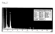
- Fig. 7 is a graph showing the results of analysis of Ag-Se nanowires obtained by energy dispersive X-ray spectroscopy (EDS). It can be seen that the composition ratio of Ag and Se constituting Ag-Se nanowires is 2:1, which is the same as the mixing ratio of the precursors (that is, Ag and Se) in the multi-component (Ag-Se) solution.
- EDS energy dispersive X-ray spectroscopy
- Figs. 8-9 show the properties of Ag-Se thin film formed on a silicon wafer by an electroplating process under the same environment as the multi-component (Ag-Se) solution in which Ag-Se nanowires are grown, which is a comparative example of Figs. 5-7 .
- gold (Au) is deposited at a thickness of 300 ⁇ 400 nm on the silicon wafer by E-beam evaporation process, and then Ag-Se thin film is formed thereon.
- Fig. 8 is a photograph of Ag-Se nanowires taken by scanning electron microscopy
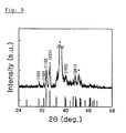
- Fig. 9 is a graph showing the results of X-ray diffraction analysis of Ag-Se thin film.
- the upper peak represents an X-ray diffraction peak of Ag-Se thin film grown by the electroplating process in this embodiment
- the lower peak represents an X-ray diffraction peak of a typical silver selenide (Ag 2 Se).
- the composition ratio of Ag-Se nanowires grown by electroplating in this embodiment is 2:1, which is the mixing ratio of Ag and Se serving as the precursors in the multi-component (Ag-Se) solution.
- the composition ratio of final multi-component nanowires can be controlled based on the mixing ratio of the precursors in the multi-component solution.
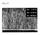
- Fig. 10 is a photograph of Ge-Sb-Te nanowires taken by scanning electron microscopy, which also shows the results of analysis of GST nanowires obtained by energy dispersive X-ray spectroscopy (EDS). It can be seen that Ge-Sb-Te nanowires are grown uniformly in an anodized aluminum oxide nanotemplate and the composition of the Ge-Sb-Te nanowires is 1:6:6.5. From this, according to the method for fabricating multi-component nanowires of the present invention, even if there are three or more types of precursors in a multi-component solution, multi-component nanowires containing all of these precursors can be fabricated.
- EDS energy dispersive X-ray spectroscopy
- Fig. 11 is a view of Ge-Sb-Te nanowires taken by transmission electron microscopy. Also, it can be found that Ge-Sb-Te nanowires are grown uniformly in an anodized aluminum oxide nanotemplate.
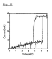
- Figs. 12 and 13 are graphs showing current changes (I-V) of Ag-Se nanowires and Ag-Se thin film, which are the results measured by using conductive atomic force microscopy (C-AFM) and 4-probe station, respectively.
- C-AFM conductive atomic force microscopy
- the method for fabricating multi-component nanowires in accordance with the present invention can fabricate multi-component nanowires in a nanotemplate having a plurality of pores by electroplating with the use of a multi-component solution, thereby making the nanowires fabrication process easier and thus offering low fabrication cost.
- the method for fabricating multi-component nanowires in accordance with the present invention has been described with respect to Ag-Se nanowires and Ge-Sb-Te nanowires that are applicable to PRAM devices, the present invention is not limited thereto but may also be applied to Ag-Se nanowire-based, Ge-Sb-Te nanowire-based ReRAM devices, and In-Se nanowire-based, Te-Se nanowire-based, and In-Ag-Se nanowire-based PRAM and ReRAM devices.
- the method for fabricating multi-component nanowires in accordance with the present invention may also be utilized in the fields of nanobiosensors, fuel cells, and biological cell isolation, in addition to the memory devices including PRAM and ReRAM.
Landscapes
- Chemical & Material Sciences (AREA)
- Engineering & Computer Science (AREA)
- Crystallography & Structural Chemistry (AREA)
- Organic Chemistry (AREA)
- Metallurgy (AREA)
- Materials Engineering (AREA)
- Electrochemistry (AREA)
- Chemical Kinetics & Catalysis (AREA)
- Nanotechnology (AREA)
- Inorganic Chemistry (AREA)
- Manufacturing & Machinery (AREA)
- Semiconductor Memories (AREA)
- Electroplating Methods And Accessories (AREA)
- Crystals, And After-Treatments Of Crystals (AREA)
Abstract
Description
- The present invention relates to a method for fabricating nanowires. More particularly, the present invention relates to a method for fabricating multi-component nanowires used to implement a nanowire-based memory device by an electroplating process using a multi-component solution.
- A phase change random access memory (PRAM) or a resistive random access memory (ReRAM), which is one of non-volatile memories, is attracting attention as a leading next generation memory device which can replace a dynamic random access memory (DRAM), which is a mainstream memory at present, owing to the advantages such as high storage speed and density, non-volatility, small size, low-power consumption and low-production cost, and so on, and thus many studies have been conducted on the PRAM and the ReRAM.
- The PRAM basically operates based on a different principle from that of a general semiconductor memory, and writes data using a phenomenon that the crystalline state of phase change materials based on chalcogenide compounds is changed by electrical switching.
- To realize a memory device of a very small size, nanowires have been suggested as an alternative for a thin film as a memory layer in the PRAM.
- Conventional nanowire fabrication methods include a vapor-liquid-solid (VLS) process (that is, an epitaxial process), a chemical vapor deposition (CVD) process, and a physical vapor deposition (PVD) process.
- However, these conventional methods has a problem that the fabrication cost is high because the price of equipment used to fabricate nanowires is high or the process takes a long time and is complicated. That is, the conventional methods have been carried out usually by sputtering, E-beam evaporation or plasma enhanced chemical vapor deposition (PECVD), but have a problem that the fabrication cost is high and the fabrication process is complicated because high-priced equipment is used and the fabrication is performed in high temperature and vacuum.
- It is, therefore, an object of the present invention to provide a method for fabricating multi-component nanowires, which makes the fabrication process easier and offers low fabrication cost by enabling it to fabricate multi-component nanowires in a nanotemplate having a plurality of pores by an electroplating process with the use of a multi-component solution.
- In accordance with one aspect of the present invention, there is provided a method for fabricating multi-component nanowires, including the steps of: (a) preparing an anodized aluminum oxide nanotemplate having a plurality of pores; (b) forming an electrode layer on one surface of the anodized aluminum oxide nanotemplate; (c) injecting the anodized aluminum oxide nanotemplate in a predetermined multi-component solution and then growing multi-component nanowires through the pores of the anodized aluminum oxide nanotemplate by an electroplating process in which the anodized aluminum oxide nanotemplate is used as a cathode; and (d) removing the anodized aluminum oxide nanotemplate.
- The diameter of the pores can be several tens to several hundreds nanometers.
- The electrode layer can comprise gold (Au).
- If the multi-component solution is an Ag-Se solution, Ag-Se nanowires can grow.
- The Ag-Se solution can include Ag and Se as precursors and nitric acid and ethylglycerol as solvents.
- If the multi-component solution is a Ge-Sb-Te solution, Ge-Sb-Te nanowires can grow.
- The Ge-Sb-Te solution can include GeO2, SbO2, and TeO2 as precursors and hydrochloric acid and ethylglycerol as solvents.
- In the step (c), a platinum electrode can be used as an anode.
- In the step (c), a composition ratio of the multi-component nanowires can be determined depending on the change of at least one of a mixing ratio of precursors in the multi-component solution and a current density applied during the electroplating process.
- In the step (d), the anodized aluminum oxide nanotemplate can be removed with a NaOH solution.
- In accordance with another aspect of the present invention, there are provided multi-component nanowires fabricated by the method disclosed above.
- The above and other objects and features of the present invention will become apparent from the following description of preferred embodiments, given in conjunction with the accompanying drawings, in which:
-
Figs. 1 to 4 are views showing the configuration of a method for fabricating multi-component nanowires in accordance with one embodiment of the present invention; -
Fig. 5 is a photograph of Ag-Se nanowires taken by scanning electron microscopy; -
Fig. 6 is a photograph of Ag-Se nanowires taken by transmission electron microscopy; -
Fig. 7 is a graph showing the results of analysis of Ag-Se nanowires obtained by energy dispersive X-ray spectroscopy; -
Fig. 8 is a photograph of Ag-Se thin film taken by a scanning electron microscopy; -
Fig. 9 is a graph showing the results of X-ray diffraction analysis of Ag-Se nanowires; -
Fig. 10 is a photograph of Ge-Sb-Te nanowires taken by scanning electron microscopy, which shows the results of analysis of Ge-Sb-Te nanowires obtained by energy dispersive X-ray spectroscopy; -
Fig. 11 is a view of Ge-Sb-Te nanowires taken by transmission electron microscopy; -
Fig. 12 is a graph showing current changes (I-V) of Ag-Se nanowires; and -
Fig. 13 is a graph showing current changes (I-V) of Ag-Se thin film. - In the following detailed description, reference is made to the accompanying drawings that show, by way of illustration, specific embodiments in which the invention may be practiced. These embodiments are described in sufficient detail to enable those skilled in the art to practice the invention. It is to be understood that the various embodiments of the invention, although different from one another, are not necessarily mutually exclusive. For example, a particular feature, structure, or characteristic described herein in connection with one embodiment may be implemented within other embodiments without departing from the spirit and scope of the present invention. Also, it should be understood that the positions or arrangements of individual elements in the embodiment may be changed without separating the spirit and scope of the present invention. The following detailed description is, therefore, not to be taken in a limiting sense, and the scope of the present invention is defined only by the appended claims that should be appropriately interpreted along with the full range of equivalents to which the claims are entitled. In the drawings, like reference numerals denote like or similar elements or functions through the several views.
- Hereinafter, the configuration of the present invention will be described in detail with reference to the accompanying drawings.
-
Figs. 1 to 4 show the configuration of a method for fabricating multi-component nanowires in accordance with one embodiment of the present invention. - First of all, referring to
Fig. 1 , an anodizedaluminum oxide nanotemplate 10 is prepared. - The anodized
aluminum oxide nanotemplate 10 having a plurality ofpores 12 formed thereon can be fabricated as follows. - First, an aluminum having a purity of 99.999% is electrochemically etched to planarize a surface thereof, and then the aluminum is anodized in oxalic acid at a voltage of 40 V and a temperature of 4°C.
- When the anodization is carried out once, the uniformity of the
pores 12 is poor, and therefore it is preferable to carry out the anodization twice in order to improve the uniformity of thepores 12. To this end, a firstly-formed anodized aluminum oxide layer is removed with chromic acid at a temperature of 65°C. The second anodization is carried out under the same condition as the first anodization. - Next, the aluminum is removed with a silver nitrate aqueous solution in order to leave only an anodized aluminum oxide layer formed by carrying out anodization twice.
- Lastly, the
pores 12 are expanded by using a phosphoric acid aqueous solution, thereby improving the uniformity of thepores 12 of the anodizedaluminum oxide nanotemplate 10. Thus, finally, the preparation of the anodizedaluminum oxide nanotemplate 10 having the plurality of thepores 12 is completed (seeFig. 1 ). - In the above procedure, the diameter of the
pores 12 formed on the anodizedaluminum oxide nanotemplate 10 is preferably several tens to several hundreds nanometers (nm). - Next, referring to
Fig. 2 , anelectrode layer 20 is formed on one surface of the anodizedaluminum oxide nanotemplate 10. - Preferably, the
electrode layer 20 is formed at a thickness of 300 to 400 nm by E-beam evaporation process on one surface of the anodizedaluminum oxide nanotemplate 10 after completion of the formation of the anodizedaluminum oxide nanotemplate 10. Here, the material of theelectrode layer 20 may comprise gold (Au). - Next, referring to
Fig. 3 ,multi-component nanowires 30 are grown through thepores 12 of the anodizedaluminum oxide nanotemplate 10 by using an electroplating process. - That is, the anodized
aluminum oxide nanotemplate 10 having the plurality ofpores 12 is injected in a multi-component solution, and then the electroplating process is carried out by using the anodizedaluminum oxide nanotemplate 10 as a cathode. - The multi-component solution used at this time may be an Ag-Se or Ge-Sb-Te solution for growing Ag-Se nanowires or Ge-Sb-Te nanowires that constitute the memory layer of the PRAM.
- In the electroplating, a platinum electrode may be used as an opposite electrode of the anodized
aluminum oxide nanotemplate 10 which is used as the cathode, i.e., an anode. Here, the purity of the platinum is preferably 99.99%. - If the multi-component solution is Ag-Se solution, the precursors may include Ag and Se and the solvents may include nitric acid and ethylglycerol. In this embodiment, in case of producing a total of 500 mℓ of Ag-Se solution, 0.1 mol of Ag, 0.05 mol of Se, 10 mℓ of nitric acid, and 100 mℓ of ethylglycerol were used.
- If the multi-component solution is Ge-Sb-Te solution, the precursors may include GeO2, SbO2, and TeO2 and the solvents may include hydrochloric acid and ethylglycerol. In this embodiment, in case of producing a total of 500 mℓ of Ge-Sb-Te solution, 0.0428 mol of GeO2, 0.0028 mol of SbO2 0.007 mol of
TeO 2 10 mℓ of hydrochloric acid, and 100 mℓ of ethylglycerol were used. - In the electroplating process of growing multi-component nanowires, a composition ratio of the multi-component nanowires can be determined depending on the change of at least one of a mixing ratio of the precursors in a multi-component solution and an applied current density.
- In this embodiment, if the multi-component solution is Ag-Se solution, the current density is preferably 2 mA/cm2, and if the multi-component solution is Ge-Sb-Te solution, the current density is preferably 1 mA/cm2.
- Lastly, referring to
Fig. 4 , the anodizedaluminum oxide nanotemplate 10 is removed, thereby finally obtainingmulti-component nanowires 30. At this time, the anodizedaluminum oxide nanotemplate 10 is preferably removed with NaOH (sodium hydroxide) solution. Afterwards, it is preferred that themulti-component nanowires 30 are washed with ultrapure water and ethanol. -
Fig. 5 is a photograph of Ag-Se nanowires taken by scanning electron microscopy (SEM). It can be seen that Ag-Se nanowires are grown uniformly in the anodized aluminum oxide nanotemplate. -
Fig. 6 is a photograph of Ag-Se nanowires taken by transmission electron microscopy (TEM). It can also be seen that Ag-Se nanowires are grown uniformly in the anodized aluminum oxide nanotemplate. -
Fig. 7 is a graph showing the results of analysis of Ag-Se nanowires obtained by energy dispersive X-ray spectroscopy (EDS). It can be seen that the composition ratio of Ag and Se constituting Ag-Se nanowires is 2:1, which is the same as the mixing ratio of the precursors (that is, Ag and Se) in the multi-component (Ag-Se) solution. -
Figs. 8-9 show the properties of Ag-Se thin film formed on a silicon wafer by an electroplating process under the same environment as the multi-component (Ag-Se) solution in which Ag-Se nanowires are grown, which is a comparative example ofFigs. 5-7 . To this end, gold (Au) is deposited at a thickness of 300∼400 nm on the silicon wafer by E-beam evaporation process, and then Ag-Se thin film is formed thereon. -
Fig. 8 is a photograph of Ag-Se nanowires taken by scanning electron microscopy, andFig. 9 is a graph showing the results of X-ray diffraction analysis of Ag-Se thin film. - In
Fig. 9 , the upper peak represents an X-ray diffraction peak of Ag-Se thin film grown by the electroplating process in this embodiment, and the lower peak represents an X-ray diffraction peak of a typical silver selenide (Ag2Se). As shown therein, considering that the upper and lower peaks match each other, it can be seen that the composition ratio of Ag-Se nanowires grown by electroplating in this embodiment is 2:1, which is the mixing ratio of Ag and Se serving as the precursors in the multi-component (Ag-Se) solution. In view of this, according to the method for fabricating multi-component nanowires of the present invention, the composition ratio of final multi-component nanowires can be controlled based on the mixing ratio of the precursors in the multi-component solution. -
Fig. 10 is a photograph of Ge-Sb-Te nanowires taken by scanning electron microscopy, which also shows the results of analysis of GST nanowires obtained by energy dispersive X-ray spectroscopy (EDS). It can be seen that Ge-Sb-Te nanowires are grown uniformly in an anodized aluminum oxide nanotemplate and the composition of the Ge-Sb-Te nanowires is 1:6:6.5. From this, according to the method for fabricating multi-component nanowires of the present invention, even if there are three or more types of precursors in a multi-component solution, multi-component nanowires containing all of these precursors can be fabricated. -
Fig. 11 is a view of Ge-Sb-Te nanowires taken by transmission electron microscopy. Also, it can be found that Ge-Sb-Te nanowires are grown uniformly in an anodized aluminum oxide nanotemplate. -
Figs. 12 and13 are graphs showing current changes (I-V) of Ag-Se nanowires and Ag-Se thin film, which are the results measured by using conductive atomic force microscopy (C-AFM) and 4-probe station, respectively. - As shown therein, both Ag-Se nanowires and Ag-Se thin film undergo an abrupt change in resistance at a certain voltage. Hence, this embodiment shows that Ag-Se nanowires grown by the electroplating process are sufficiently applicable to a nanowire-based PRAM device.
- As described above, the method for fabricating multi-component nanowires in accordance with the present invention can fabricate multi-component nanowires in a nanotemplate having a plurality of pores by electroplating with the use of a multi-component solution, thereby making the nanowires fabrication process easier and thus offering low fabrication cost.
- Although the method for fabricating multi-component nanowires in accordance with the present invention has been described with respect to Ag-Se nanowires and Ge-Sb-Te nanowires that are applicable to PRAM devices, the present invention is not limited thereto but may also be applied to Ag-Se nanowire-based, Ge-Sb-Te nanowire-based ReRAM devices, and In-Se nanowire-based, Te-Se nanowire-based, and In-Ag-Se nanowire-based PRAM and ReRAM devices.
- Further, the method for fabricating multi-component nanowires in accordance with the present invention may also be utilized in the fields of nanobiosensors, fuel cells, and biological cell isolation, in addition to the memory devices including PRAM and ReRAM.
- While the present invention has been described with respect to certain preferred embodiments, it will be apparent to those skilled in the art that various changes and modifications may be made without departing from the scope of the invention as defined in the following claims.
Claims (11)
- A method for fabricating multi-component nanowires, comprising the steps of:(a) preparing an anodized aluminum oxide nanotemplate having a plurality of pores;(b) forming an electrode layer on one surface of the anodized aluminum oxide nanotemplate;(c) injecting the anodized aluminum oxide nanotemplate in a predetermined multi-component solution and then growing multi-component nanowires through the pores of the anodized aluminum oxide nanotemplate by an electroplating process in which the anodized aluminum oxide nanotemplate is used as a cathode; and(d) removing the anodized aluminum oxide nanotemplate.
- The method of claim 1, wherein the diameter of the pores is several tens to several hundreds nanometers.
- The method of claim 1, wherein the electrode layer comprises gold (Au).
- The method of claim 1, wherein if the multi-component solution is an Ag-Se solution, Ag-Se nanowires grow.
- The method of claim 4, wherein the Ag-Se solution includes Ag and Se as precursors and nitric acid and ethylglycerol as solvents.
- The method of claim 1, wherein if the multi-component solution is a Ge-Sb-Te solution, Ge-Sb-Te nanowires grow.
- The method of claim 6, wherein the Ge-Sb-Te solution includes GeO2, SbO2, and TeO2 as precursors and hydrochloric acid and ethylglycerol as solvents.
- The method of claim 1, wherein in said step (c), a platinum electrode is used as an anode.
- The method of claim 1, wherein in said step (c), a composition ratio of the multi-component nanowires is determined depending on the change of at least one of a mixing ratio of precursors in the multi-component solution and a current density applied during the electroplating process.
- The method of claim 1, wherein in said step (d), the anodized aluminum oxide nanotemplate is removed with a NaOH solution.
- Multi-component nanowires fabricated by the method of any one of claims 1 to 10.
Applications Claiming Priority (1)
| Application Number | Priority Date | Filing Date | Title |
|---|---|---|---|
| KR1020080137859A KR101093364B1 (en) | 2008-12-31 | 2008-12-31 | Method of manufacturing polycyclic nanowires |
Publications (2)
| Publication Number | Publication Date |
|---|---|
| EP2204474A1 true EP2204474A1 (en) | 2010-07-07 |
| EP2204474B1 EP2204474B1 (en) | 2012-08-01 |
Family
ID=41478678
Family Applications (1)
| Application Number | Title | Priority Date | Filing Date |
|---|---|---|---|
| EP09011927A Active EP2204474B1 (en) | 2008-12-31 | 2009-09-18 | Method for fabricating Ge-Sb-Te nanowires |
Country Status (4)
| Country | Link |
|---|---|
| US (1) | US20100163419A1 (en) |
| EP (1) | EP2204474B1 (en) |
| JP (2) | JP2010156038A (en) |
| KR (1) | KR101093364B1 (en) |
Families Citing this family (8)
| Publication number | Priority date | Publication date | Assignee | Title |
|---|---|---|---|---|
| JP2789836B2 (en) | 1991-03-20 | 1998-08-27 | 王子製紙株式会社 | Sheet stacking and unloading device |
| KR101332422B1 (en) * | 2011-01-07 | 2013-12-02 | 건국대학교 산학협력단 | Templated electrochemical growth of single-crystal Cu2O nanowire arrays |
| CN102330058B (en) * | 2011-09-20 | 2013-07-03 | 北京航空航天大学 | Method for preparing multi-grade antimonytelluride nano wire harness array by adopting physical vapor deposition |
| KR101411332B1 (en) | 2013-12-17 | 2014-06-27 | 연세대학교 산학협력단 | Implanted-ion assisted growth method of metal oxide Nanowire and pattening device using the method |
| CN104803348A (en) * | 2015-04-20 | 2015-07-29 | 中国科学院光电技术研究所 | Method for preparing high-aspect-ratio polymer nano-pillar array by using sacrificial template |
| CN109795975A (en) * | 2018-12-28 | 2019-05-24 | 南京大学 | A kind of metal micro-/ nano linear array and preparation method thereof |
| CN110310891B (en) * | 2019-06-28 | 2021-10-01 | 惠科股份有限公司 | Preparation method of metal nanowire conductive film and thin film transistor |
| CN118299445B (en) * | 2024-06-06 | 2024-08-16 | 中北大学 | Self-powered photoelectric detection device with wide spectral response and preparation method thereof |
Citations (2)
| Publication number | Priority date | Publication date | Assignee | Title |
|---|---|---|---|---|
| EP1925696A2 (en) | 2006-11-01 | 2008-05-28 | KOREA University, Industry & Academy Collaboration Foundation of Korea University, Industry & Academy Collaboration Foundation | Iron-gold barcode nanowire and manufacturing method thereof |
| US20080156654A1 (en) | 2006-08-08 | 2008-07-03 | Joseph Wang | Identification Based On Compositionally Encoded Nanostructures |
Family Cites Families (12)
| Publication number | Priority date | Publication date | Assignee | Title |
|---|---|---|---|---|
| JPH10106047A (en) * | 1996-10-01 | 1998-04-24 | Sony Corp | Manufacturing method of optical recording medium |
| JP3675326B2 (en) * | 2000-10-06 | 2005-07-27 | キヤノン株式会社 | Multi-channel plate manufacturing method |
| JP2002150626A (en) * | 2000-11-13 | 2002-05-24 | Mitsubishi Chemicals Corp | Manufacturing method of stamper and information recording medium |
| JP3899413B2 (en) * | 2004-03-12 | 2007-03-28 | 独立行政法人物質・材料研究機構 | Nanomaterial fabrication method |
| JP2006140334A (en) * | 2004-11-12 | 2006-06-01 | Canon Inc | Thermoelectric conversion element |
| FR2885913B1 (en) * | 2005-05-18 | 2007-08-10 | Centre Nat Rech Scient | COMPOSITE ELEMENT COMPRISING A CONDUCTIVE SUBSTRATE AND A NANOSTRUCTURED METAL COATING. |
| JP4364180B2 (en) * | 2005-08-17 | 2009-11-11 | 株式会社東芝 | Manufacturing method of integrated circuit device |
| JP5361130B2 (en) * | 2005-08-26 | 2013-12-04 | 公益財団法人神奈川科学技術アカデミー | Porous polymer membrane and method for producing the same |
| KR100747074B1 (en) | 2006-10-25 | 2007-08-07 | 금오공과대학교 산학협력단 | Method for producing nanorods using anodized aluminum oxide template (AOOTHemTolerance) and nanorods obtained using the same |
| KR100817535B1 (en) | 2007-01-19 | 2008-03-27 | 한양대학교 산학협력단 | Semiconductor nanowires and manufacturing method thereof, and semiconductor device comprising the same |
| US7918984B2 (en) * | 2007-09-17 | 2011-04-05 | International Business Machines Corporation | Method of electrodepositing germanium compound materials on a substrate |
| US20090243584A1 (en) * | 2008-03-25 | 2009-10-01 | Guigen Zhang | Fabrication of microstructures integrated with nanopillars along with their applications as electrodes in sensors |
-
2008
- 2008-12-31 KR KR1020080137859A patent/KR101093364B1/en active Active
-
2009
- 2009-09-16 JP JP2009214183A patent/JP2010156038A/en active Pending
- 2009-09-18 EP EP09011927A patent/EP2204474B1/en active Active
- 2009-09-24 US US12/566,431 patent/US20100163419A1/en not_active Abandoned
-
2013
- 2013-06-11 JP JP2013122472A patent/JP5525090B2/en active Active
Patent Citations (2)
| Publication number | Priority date | Publication date | Assignee | Title |
|---|---|---|---|---|
| US20080156654A1 (en) | 2006-08-08 | 2008-07-03 | Joseph Wang | Identification Based On Compositionally Encoded Nanostructures |
| EP1925696A2 (en) | 2006-11-01 | 2008-05-28 | KOREA University, Industry & Academy Collaboration Foundation of Korea University, Industry & Academy Collaboration Foundation | Iron-gold barcode nanowire and manufacturing method thereof |
Non-Patent Citations (6)
| Title |
|---|
| CHEN ET AL.: "Silver Selenide Nanowires by Electrodeposition", J. ELECTROCHEMICAL SOCIETY, vol. 150, no. 3, 28 January 2003 (2003-01-28), pages G183 - G186 |
| CHEN ET AL: "Silver selenide nanowires by electrodeposition", J. ELECTROCHEMICAL SOCIETY, vol. 150, no. 3, 28 January 2003 (2003-01-28), USA, pages G183 - G186, XP002562979 * |
| CHUANGUI JIN ET AL.: "Large-area Sb2Te3 nanowire arrays", J. PHYS. CHEM. B, vol. 109, no. 4, 2005, pages 1430 - 1432 |
| CHUANGUI JIN ET AL: "Large-area Sb2Te3 nanowire arrays", J.PHYS.CHEM B, vol. 109, no. 4, 2005, pages 1430 - 1432, XP002562980 * |
| VENKATASAMY ET AL.: "ALD approach toward electrodeposition of Sb2Te3 for phase-change memory application", J. ELECTROCHEM. SOC., vol. 155, no. 11, pages D693 - D698 |
| VENKATASAMY ET AL.: "ALD approach toward electrodeposition of Sb2Te3 for phase-change memory applications", J.ELECTROCHEM. SOC., vol. 155, no. 11, 5 November 2008 (2008-11-05), USA, pages D693 - D698, XP002562981 * |
Also Published As
| Publication number | Publication date |
|---|---|
| JP5525090B2 (en) | 2014-06-18 |
| JP2013177696A (en) | 2013-09-09 |
| US20100163419A1 (en) | 2010-07-01 |
| KR101093364B1 (en) | 2011-12-14 |
| KR20100079391A (en) | 2010-07-08 |
| EP2204474B1 (en) | 2012-08-01 |
| JP2010156038A (en) | 2010-07-15 |
Similar Documents
| Publication | Publication Date | Title |
|---|---|---|
| US20100163419A1 (en) | Method for fabricating multi-component nanowires | |
| US9281476B2 (en) | Resistive memory and method for fabricating the same | |
| US20140217354A1 (en) | Large array of upward pointing p-i-n diodes having large and uniform current | |
| US11227995B2 (en) | Si2Te3 resistive memory | |
| WO2013043410A1 (en) | Methods and apparatus for including an air gap in carbon-based memory devices | |
| CA2324927A1 (en) | Memory element with memory material comprising phase-change material and dielectric material | |
| EP2539936A2 (en) | Memory cell with silicon-containing carbon switching layer and methods for forming the same | |
| US20110133151A1 (en) | Memory cell that includes a carbon-based memory element and methods of forming the same | |
| WO2010078467A1 (en) | Modulation of resistivity in carbon-based read-writeable materials | |
| US20120085985A1 (en) | Electrically actuated device | |
| CN102544355B (en) | Phase-change storage material and preparation method thereof as well as storage device provided therewith and preparation method thereof | |
| CN100397561C (en) | A kind of preparation method of nanophase change memory device unit | |
| CN101976675B (en) | Phase change memory using wide band gap semiconductor diode as gating tube and method | |
| US20110182115A1 (en) | METHOD FOR FABRICATING INDIUM (In)-ANTIMONY (Sb)-TELLURIUM (Te) NANOWIRES AND PHASE-CHANGE MEMORY DEVICE COMPRISING THE NANOWIRES | |
| US12284925B2 (en) | Memory device having a switching element thicker at a first side than at a second side and method of forming the same | |
| KR101092424B1 (en) | Method for forming In-Sb-Te thin film by chemical vapor deposition and method for manufacturing phase-change memory device using the same | |
| WO2011109271A1 (en) | A memory cell that includes a carbon-based memory element and methods of forming the same | |
| CN101599531B (en) | A storage unit of resistive random access memory and its preparation method | |
| KR101764336B1 (en) | Bottom-up resistive random access memory and method of fabricating the same | |
| US11713518B2 (en) | Method for forming chalcogenide thin film | |
| Pham et al. | Surface Mapping of Resistive Switching CrOx Thin Films | |
| CN103540976B (en) | A kind of telluro ternary heterojunction nanowire and preparation method thereof | |
| Kumar et al. | Resistive switching in copper oxide nanorods: a bottom up approach applicable for enhanced scalability | |
| Shi-Long et al. | High speed and ultra-low-power phase change line cell memory based on SiSb thin films with nanoscale gap of electrodes less than 100 nm | |
| AU2001281595B2 (en) | Single molecule array on silicon substrate for quantum computer |
Legal Events
| Date | Code | Title | Description |
|---|---|---|---|
| PUAI | Public reference made under article 153(3) epc to a published international application that has entered the european phase |
Free format text: ORIGINAL CODE: 0009012 |
|
| AK | Designated contracting states |
Kind code of ref document: A1 Designated state(s): AT BE BG CH CY CZ DE DK EE ES FI FR GB GR HR HU IE IS IT LI LT LU LV MC MK MT NL NO PL PT RO SE SI SK SM TR |
|
| AX | Request for extension of the european patent |
Extension state: AL BA RS |
|
| 17P | Request for examination filed |
Effective date: 20101209 |
|
| 17Q | First examination report despatched |
Effective date: 20110822 |
|
| GRAP | Despatch of communication of intention to grant a patent |
Free format text: ORIGINAL CODE: EPIDOSNIGR1 |
|
| RIC1 | Information provided on ipc code assigned before grant |
Ipc: C30B 29/60 20060101ALI20120109BHEP Ipc: C25D 1/04 20060101AFI20120109BHEP Ipc: C30B 7/12 20060101ALI20120109BHEP Ipc: C30B 29/46 20060101ALI20120109BHEP |
|
| RTI1 | Title (correction) |
Free format text: METHOD FOR FABRICATING GE-SB-TE NANOWIRES |
|
| GRAS | Grant fee paid |
Free format text: ORIGINAL CODE: EPIDOSNIGR3 |
|
| GRAA | (expected) grant |
Free format text: ORIGINAL CODE: 0009210 |
|
| AK | Designated contracting states |
Kind code of ref document: B1 Designated state(s): AT BE BG CH CY CZ DE DK EE ES FI FR GB GR HR HU IE IS IT LI LT LU LV MC MK MT NL NO PL PT RO SE SI SK SM TR |
|
| REG | Reference to a national code |
Ref country code: GB Ref legal event code: FG4D |
|
| REG | Reference to a national code |
Ref country code: AT Ref legal event code: REF Ref document number: 568773 Country of ref document: AT Kind code of ref document: T Effective date: 20120815 Ref country code: CH Ref legal event code: EP |
|
| REG | Reference to a national code |
Ref country code: IE Ref legal event code: FG4D |
|
| REG | Reference to a national code |
Ref country code: DE Ref legal event code: R096 Ref document number: 602009008575 Country of ref document: DE Effective date: 20120927 |
|
| REG | Reference to a national code |
Ref country code: NL Ref legal event code: VDEP Effective date: 20120801 |
|
| REG | Reference to a national code |
Ref country code: AT Ref legal event code: MK05 Ref document number: 568773 Country of ref document: AT Kind code of ref document: T Effective date: 20120801 |
|
| REG | Reference to a national code |
Ref country code: LT Ref legal event code: MG4D Effective date: 20120801 |
|
| PG25 | Lapsed in a contracting state [announced via postgrant information from national office to epo] |
Ref country code: IS Free format text: LAPSE BECAUSE OF FAILURE TO SUBMIT A TRANSLATION OF THE DESCRIPTION OR TO PAY THE FEE WITHIN THE PRESCRIBED TIME-LIMIT Effective date: 20121201 Ref country code: CY Free format text: LAPSE BECAUSE OF FAILURE TO SUBMIT A TRANSLATION OF THE DESCRIPTION OR TO PAY THE FEE WITHIN THE PRESCRIBED TIME-LIMIT Effective date: 20120801 Ref country code: FI Free format text: LAPSE BECAUSE OF FAILURE TO SUBMIT A TRANSLATION OF THE DESCRIPTION OR TO PAY THE FEE WITHIN THE PRESCRIBED TIME-LIMIT Effective date: 20120801 Ref country code: LT Free format text: LAPSE BECAUSE OF FAILURE TO SUBMIT A TRANSLATION OF THE DESCRIPTION OR TO PAY THE FEE WITHIN THE PRESCRIBED TIME-LIMIT Effective date: 20120801 Ref country code: HR Free format text: LAPSE BECAUSE OF FAILURE TO SUBMIT A TRANSLATION OF THE DESCRIPTION OR TO PAY THE FEE WITHIN THE PRESCRIBED TIME-LIMIT Effective date: 20120801 Ref country code: NO Free format text: LAPSE BECAUSE OF FAILURE TO SUBMIT A TRANSLATION OF THE DESCRIPTION OR TO PAY THE FEE WITHIN THE PRESCRIBED TIME-LIMIT Effective date: 20121101 Ref country code: AT Free format text: LAPSE BECAUSE OF FAILURE TO SUBMIT A TRANSLATION OF THE DESCRIPTION OR TO PAY THE FEE WITHIN THE PRESCRIBED TIME-LIMIT Effective date: 20120801 |
|
| PG25 | Lapsed in a contracting state [announced via postgrant information from national office to epo] |
Ref country code: PL Free format text: LAPSE BECAUSE OF FAILURE TO SUBMIT A TRANSLATION OF THE DESCRIPTION OR TO PAY THE FEE WITHIN THE PRESCRIBED TIME-LIMIT Effective date: 20120801 Ref country code: GR Free format text: LAPSE BECAUSE OF FAILURE TO SUBMIT A TRANSLATION OF THE DESCRIPTION OR TO PAY THE FEE WITHIN THE PRESCRIBED TIME-LIMIT Effective date: 20121102 Ref country code: BE Free format text: LAPSE BECAUSE OF FAILURE TO SUBMIT A TRANSLATION OF THE DESCRIPTION OR TO PAY THE FEE WITHIN THE PRESCRIBED TIME-LIMIT Effective date: 20120801 Ref country code: SI Free format text: LAPSE BECAUSE OF FAILURE TO SUBMIT A TRANSLATION OF THE DESCRIPTION OR TO PAY THE FEE WITHIN THE PRESCRIBED TIME-LIMIT Effective date: 20120801 Ref country code: SE Free format text: LAPSE BECAUSE OF FAILURE TO SUBMIT A TRANSLATION OF THE DESCRIPTION OR TO PAY THE FEE WITHIN THE PRESCRIBED TIME-LIMIT Effective date: 20120801 Ref country code: LV Free format text: LAPSE BECAUSE OF FAILURE TO SUBMIT A TRANSLATION OF THE DESCRIPTION OR TO PAY THE FEE WITHIN THE PRESCRIBED TIME-LIMIT Effective date: 20120801 Ref country code: PT Free format text: LAPSE BECAUSE OF FAILURE TO SUBMIT A TRANSLATION OF THE DESCRIPTION OR TO PAY THE FEE WITHIN THE PRESCRIBED TIME-LIMIT Effective date: 20121203 |
|
| PG25 | Lapsed in a contracting state [announced via postgrant information from national office to epo] |
Ref country code: NL Free format text: LAPSE BECAUSE OF FAILURE TO SUBMIT A TRANSLATION OF THE DESCRIPTION OR TO PAY THE FEE WITHIN THE PRESCRIBED TIME-LIMIT Effective date: 20120801 |
|
| PG25 | Lapsed in a contracting state [announced via postgrant information from national office to epo] |
Ref country code: EE Free format text: LAPSE BECAUSE OF FAILURE TO SUBMIT A TRANSLATION OF THE DESCRIPTION OR TO PAY THE FEE WITHIN THE PRESCRIBED TIME-LIMIT Effective date: 20120801 Ref country code: MC Free format text: LAPSE BECAUSE OF NON-PAYMENT OF DUE FEES Effective date: 20120930 Ref country code: RO Free format text: LAPSE BECAUSE OF FAILURE TO SUBMIT A TRANSLATION OF THE DESCRIPTION OR TO PAY THE FEE WITHIN THE PRESCRIBED TIME-LIMIT Effective date: 20120801 Ref country code: DK Free format text: LAPSE BECAUSE OF FAILURE TO SUBMIT A TRANSLATION OF THE DESCRIPTION OR TO PAY THE FEE WITHIN THE PRESCRIBED TIME-LIMIT Effective date: 20120801 Ref country code: CZ Free format text: LAPSE BECAUSE OF FAILURE TO SUBMIT A TRANSLATION OF THE DESCRIPTION OR TO PAY THE FEE WITHIN THE PRESCRIBED TIME-LIMIT Effective date: 20120801 Ref country code: ES Free format text: LAPSE BECAUSE OF FAILURE TO SUBMIT A TRANSLATION OF THE DESCRIPTION OR TO PAY THE FEE WITHIN THE PRESCRIBED TIME-LIMIT Effective date: 20121112 |
|
| PG25 | Lapsed in a contracting state [announced via postgrant information from national office to epo] |
Ref country code: IT Free format text: LAPSE BECAUSE OF FAILURE TO SUBMIT A TRANSLATION OF THE DESCRIPTION OR TO PAY THE FEE WITHIN THE PRESCRIBED TIME-LIMIT Effective date: 20120801 Ref country code: SK Free format text: LAPSE BECAUSE OF FAILURE TO SUBMIT A TRANSLATION OF THE DESCRIPTION OR TO PAY THE FEE WITHIN THE PRESCRIBED TIME-LIMIT Effective date: 20120801 |
|
| PLBE | No opposition filed within time limit |
Free format text: ORIGINAL CODE: 0009261 |
|
| STAA | Information on the status of an ep patent application or granted ep patent |
Free format text: STATUS: NO OPPOSITION FILED WITHIN TIME LIMIT |
|
| REG | Reference to a national code |
Ref country code: IE Ref legal event code: MM4A |
|
| 26N | No opposition filed |
Effective date: 20130503 |
|
| PG25 | Lapsed in a contracting state [announced via postgrant information from national office to epo] |
Ref country code: BG Free format text: LAPSE BECAUSE OF FAILURE TO SUBMIT A TRANSLATION OF THE DESCRIPTION OR TO PAY THE FEE WITHIN THE PRESCRIBED TIME-LIMIT Effective date: 20121101 Ref country code: IE Free format text: LAPSE BECAUSE OF NON-PAYMENT OF DUE FEES Effective date: 20120918 |
|
| REG | Reference to a national code |
Ref country code: DE Ref legal event code: R097 Ref document number: 602009008575 Country of ref document: DE Effective date: 20130503 |
|
| PG25 | Lapsed in a contracting state [announced via postgrant information from national office to epo] |
Ref country code: MT Free format text: LAPSE BECAUSE OF FAILURE TO SUBMIT A TRANSLATION OF THE DESCRIPTION OR TO PAY THE FEE WITHIN THE PRESCRIBED TIME-LIMIT Effective date: 20120801 |
|
| PG25 | Lapsed in a contracting state [announced via postgrant information from national office to epo] |
Ref country code: TR Free format text: LAPSE BECAUSE OF FAILURE TO SUBMIT A TRANSLATION OF THE DESCRIPTION OR TO PAY THE FEE WITHIN THE PRESCRIBED TIME-LIMIT Effective date: 20120801 |
|
| REG | Reference to a national code |
Ref country code: CH Ref legal event code: PL |
|
| PG25 | Lapsed in a contracting state [announced via postgrant information from national office to epo] |
Ref country code: SM Free format text: LAPSE BECAUSE OF FAILURE TO SUBMIT A TRANSLATION OF THE DESCRIPTION OR TO PAY THE FEE WITHIN THE PRESCRIBED TIME-LIMIT Effective date: 20120801 Ref country code: LU Free format text: LAPSE BECAUSE OF NON-PAYMENT OF DUE FEES Effective date: 20120918 |
|
| PG25 | Lapsed in a contracting state [announced via postgrant information from national office to epo] |
Ref country code: HU Free format text: LAPSE BECAUSE OF FAILURE TO SUBMIT A TRANSLATION OF THE DESCRIPTION OR TO PAY THE FEE WITHIN THE PRESCRIBED TIME-LIMIT Effective date: 20090918 Ref country code: CH Free format text: LAPSE BECAUSE OF NON-PAYMENT OF DUE FEES Effective date: 20130930 Ref country code: LI Free format text: LAPSE BECAUSE OF NON-PAYMENT OF DUE FEES Effective date: 20130930 |
|
| PG25 | Lapsed in a contracting state [announced via postgrant information from national office to epo] |
Ref country code: MK Free format text: LAPSE BECAUSE OF FAILURE TO SUBMIT A TRANSLATION OF THE DESCRIPTION OR TO PAY THE FEE WITHIN THE PRESCRIBED TIME-LIMIT Effective date: 20120801 |
|
| REG | Reference to a national code |
Ref country code: FR Ref legal event code: PLFP Year of fee payment: 7 |
|
| REG | Reference to a national code |
Ref country code: FR Ref legal event code: PLFP Year of fee payment: 8 |
|
| REG | Reference to a national code |
Ref country code: FR Ref legal event code: PLFP Year of fee payment: 9 |
|
| REG | Reference to a national code |
Ref country code: FR Ref legal event code: PLFP Year of fee payment: 10 |
|
| PGFP | Annual fee paid to national office [announced via postgrant information from national office to epo] |
Ref country code: DE Payment date: 20250904 Year of fee payment: 17 |
|
| PGFP | Annual fee paid to national office [announced via postgrant information from national office to epo] |
Ref country code: GB Payment date: 20250904 Year of fee payment: 17 |
|
| PGFP | Annual fee paid to national office [announced via postgrant information from national office to epo] |
Ref country code: FR Payment date: 20250904 Year of fee payment: 17 |