EP2204346A1 - Thermal fluid flow sensor and method of manufacturing the same - Google Patents
Thermal fluid flow sensor and method of manufacturing the same Download PDFInfo
- Publication number
- EP2204346A1 EP2204346A1 EP09015011A EP09015011A EP2204346A1 EP 2204346 A1 EP2204346 A1 EP 2204346A1 EP 09015011 A EP09015011 A EP 09015011A EP 09015011 A EP09015011 A EP 09015011A EP 2204346 A1 EP2204346 A1 EP 2204346A1
- Authority
- EP
- European Patent Office
- Prior art keywords
- film
- resistive element
- temperature
- fluid flow
- heater
- Prior art date
- Legal status (The legal status is an assumption and is not a legal conclusion. Google has not performed a legal analysis and makes no representation as to the accuracy of the status listed.)
- Granted
Links
Images






Classifications
-
- B—PERFORMING OPERATIONS; TRANSPORTING
- B81—MICROSTRUCTURAL TECHNOLOGY
- B81B—MICROSTRUCTURAL DEVICES OR SYSTEMS, e.g. MICROMECHANICAL DEVICES
- B81B3/00—Devices comprising flexible or deformable elements, e.g. comprising elastic tongues or membranes
- B81B3/0064—Constitution or structural means for improving or controlling the physical properties of a device
- B81B3/0067—Mechanical properties
- B81B3/0072—For controlling internal stress or strain in moving or flexible elements, e.g. stress compensating layers
-
- G—PHYSICS
- G01—MEASURING; TESTING
- G01F—MEASURING VOLUME, VOLUME FLOW, MASS FLOW OR LIQUID LEVEL; METERING BY VOLUME
- G01F1/00—Measuring the volume flow or mass flow of fluid or fluent solid material wherein the fluid passes through a meter in a continuous flow
- G01F1/68—Measuring the volume flow or mass flow of fluid or fluent solid material wherein the fluid passes through a meter in a continuous flow by using thermal effects
- G01F1/684—Structural arrangements; Mounting of elements, e.g. in relation to fluid flow
- G01F1/6845—Micromachined devices
-
- G—PHYSICS
- G01—MEASURING; TESTING
- G01F—MEASURING VOLUME, VOLUME FLOW, MASS FLOW OR LIQUID LEVEL; METERING BY VOLUME
- G01F1/00—Measuring the volume flow or mass flow of fluid or fluent solid material wherein the fluid passes through a meter in a continuous flow
- G01F1/68—Measuring the volume flow or mass flow of fluid or fluent solid material wherein the fluid passes through a meter in a continuous flow by using thermal effects
- G01F1/684—Structural arrangements; Mounting of elements, e.g. in relation to fluid flow
- G01F1/688—Structural arrangements; Mounting of elements, e.g. in relation to fluid flow using a particular type of heating, cooling or sensing element
- G01F1/69—Structural arrangements; Mounting of elements, e.g. in relation to fluid flow using a particular type of heating, cooling or sensing element of resistive type
- G01F1/692—Thin-film arrangements
-
- G—PHYSICS
- G01—MEASURING; TESTING
- G01F—MEASURING VOLUME, VOLUME FLOW, MASS FLOW OR LIQUID LEVEL; METERING BY VOLUME
- G01F1/00—Measuring the volume flow or mass flow of fluid or fluent solid material wherein the fluid passes through a meter in a continuous flow
- G01F1/68—Measuring the volume flow or mass flow of fluid or fluent solid material wherein the fluid passes through a meter in a continuous flow by using thermal effects
- G01F1/696—Circuits therefor, e.g. constant-current flow meters
- G01F1/698—Feedback or rebalancing circuits, e.g. self heated constant temperature flowmeters
- G01F1/699—Feedback or rebalancing circuits, e.g. self heated constant temperature flowmeters by control of a separate heating or cooling element
-
- G—PHYSICS
- G01—MEASURING; TESTING
- G01F—MEASURING VOLUME, VOLUME FLOW, MASS FLOW OR LIQUID LEVEL; METERING BY VOLUME
- G01F5/00—Measuring a proportion of the volume flow
-
- B—PERFORMING OPERATIONS; TRANSPORTING
- B81—MICROSTRUCTURAL TECHNOLOGY
- B81B—MICROSTRUCTURAL DEVICES OR SYSTEMS, e.g. MICROMECHANICAL DEVICES
- B81B2201/00—Specific applications of microelectromechanical systems
- B81B2201/02—Sensors
- B81B2201/0292—Sensors not provided for in B81B2201/0207 - B81B2201/0285
-
- B—PERFORMING OPERATIONS; TRANSPORTING
- B81—MICROSTRUCTURAL TECHNOLOGY
- B81B—MICROSTRUCTURAL DEVICES OR SYSTEMS, e.g. MICROMECHANICAL DEVICES
- B81B2203/00—Basic microelectromechanical structures
- B81B2203/01—Suspended structures, i.e. structures allowing a movement
- B81B2203/0127—Diaphragms, i.e. structures separating two media that can control the passage from one medium to another; Membranes, i.e. diaphragms with filtering function
-
- Y—GENERAL TAGGING OF NEW TECHNOLOGICAL DEVELOPMENTS; GENERAL TAGGING OF CROSS-SECTIONAL TECHNOLOGIES SPANNING OVER SEVERAL SECTIONS OF THE IPC; TECHNICAL SUBJECTS COVERED BY FORMER USPC CROSS-REFERENCE ART COLLECTIONS [XRACs] AND DIGESTS
- Y10—TECHNICAL SUBJECTS COVERED BY FORMER USPC
- Y10T—TECHNICAL SUBJECTS COVERED BY FORMER US CLASSIFICATION
- Y10T29/00—Metal working
- Y10T29/49—Method of mechanical manufacture
- Y10T29/49002—Electrical device making
- Y10T29/49082—Resistor making
- Y10T29/49083—Heater type
Definitions
- the total film thickness of the insulating film in the diaphragm has a large difference between a portion without the wirings and the heater portion and the sensor portion of the microprocessed wirings, resulting in a deflection due to an imbalance of stress.
- hatching is used even in a plan view so as to make the drawings easy to see.
- a measuring element 1 which is the thermal fluid flow sensor of the first embodiment is composed of a semiconductor substrate 2, a heater resistive element 3, a temperature-measuring resistive element for heater resistive element 4, a temperature-measuring resistive element, an air-temperature-measuring resistive element 6, heater-temperature-controlling resistive elements 7 and 8, terminal electrodes 9A to 9I, and draw-out wirings 10A, 10B, 10C1,10C2, 10D, 10E, 10F, 10G, 10H1, 10H2, 10I1, and 10I2, etc.
- the measuring element 1 measures the air temperature of an air flow 13 by the air-temperature-measuring resistive element 6, and calculates a temperature difference ( ⁇ Th) by comparing the measured air temperature with a resistance increase of the temperature-measuring resistive element for heater resistive element 4 heated by the heater resistive element 3, and resistances of the temperature-measuring resistive elements 5A, 5B, 5C, and 5D are changed by the air flow warmed by the heater resistive element 3.
- the wiring structure is in a loopback meandering pattern to match the resistance values of the respective resistive elements and setting values.
- a barrier metal film of, for example, a TiN (titanium nitride) film can be formed as a third metal film before depositing the Al alloy film to form a stacked film of the barrier metal film and the Al alloy film.
- the contact resistance is increased when the barrier metal film is formed to be relatively thick, the thickness of the barrier metal film is preferable to be about 20 nm. Meanwhile, if the problem of increasing resistance can be avoided as an efficient contact area is ensured, the thickness of the barrier metal film can be smaller than or equal to 200 nm.
- the second metal film 24 is patterned by dry etching or wet etching using a photolithography method to form the terminal electrodes 9A to 9I.
- a protective film 25 on the terminal electrodes 9A to 91 e.g., a polyimide film is formed, and the opening 11 and an opening (not illustrated) for connecting the terminal electrodes 9A to 9I and the external circuit(s) are formed on at least the heater resistive element 3, the temperature-measuring resistive element for heater resistive element 4, the upstream temperature-measuring resistive elements 5A and 5B, and the downstream temperature-measuring resistive elements 5C and 5D by etching using a photolithography method.
- the protective film 25 can be a photo-sensitive organic film having a thickness of 2 to 3 ⁇ m.
- the circuit illustrated in FIG 11 has two bridge circuits, one of them is a heater-controlling bridge circuit composed of the temperature-measuring resistive element for heater resistive element 4, the air-temperature-measuring resistive element 6, and the heater-temperature-controlling resistive elements 7 and 8, and the other is a temperature-sensor bridge circuit composed of the four temperature-measuring resistive elements (the upstream temperature-measuring resistive elements 5A and 5B and the downstream temperature-measuring resistive elements 5C and 5D).
- the terminal electrode 9D electrically connected to both of the temperature-measuring resistive element for heater resistive element 4 and the heater-temperature-controlling resistive element 7 via the draw-out wiring 10D corresponds to a node A in FIG 11 .
- terminal electrode 9E electrically connected to both of the air-temperature-measuring resistive element 6 and the heater-temperature-controlling resistive element 8 via the draw-out wiring 10E corresponds to a node B in FIG 11 .
- terminal electrode 9I electrically connected to both of the upstream temperature-measuring resistive element 5A and the downstream temperature-measuring resistive element 5D via the two draw-out wirings 10I1 and 10I2 corresponds to a node C in FIG 11 .
- respective resistance values of the temperature-measuring resistive element for heater resistive element 4, the air-temperature-measuring resistive element 6, and the heater-temperature-controlling resistive elements 7 and 8 are set to make a potential difference between the node A (terminal electrode 9D) and the node B (terminal electrode 9E) to be 0 V when a gas heated by the heater resistive element 3 is at a temperature higher than the intake air temperature by a fixed temperature ( ⁇ Th, e.g., 100°C).
- ⁇ Th e.g. 100°C
- the heater-controlling bridge circuit is designed to change the current in the heater resistive element 3 with controlling the transistor 34 by the control circuit 35, so that the bridge circuit is maintained at an equilibrium state (potential difference between A and B is 0 V).
- a pitch of sensor wirings (the upstream temperature-measuring resistive elements 5A and 5B and the downstream temperature-measuring resistive elements 5C and 5D) is set to about 1.2 ⁇ m, and a pitch of the heater wirings (the heater resistive element 3) is set to about 20 ⁇ m, and a shift amount of the surface of the sensor is illustrated in FIG 12 .
- a silicon oxide film (the first insulating film 14) formed on the semiconductor substrate 2 by a thermal treatment is about 200 nm
- a silicon nitride film (the second insulating film 15) formed by a CVD method is about 200 nm
- a silicon oxide film (the third insulating film 16) deposited by a CVD method is about 350 nm
- a silicon nitride film (the fourth insulating film 17) for compensating the tensile stress of the silicon nitride film above is about 140 nm
- a silicon oxide film (the fifth insulating film 18) above the silicon nitride film is about 150 nm
- a Mo film the heater resistive element 3, the temperature-measuring resistive element for heater resistive element 4, the temperature-measuring resistive element (the upstream temperature-measuring resistive elements 5A and 5B and the downstream temperature-measuring resistive elements 5C and
- the shift amount of the surface of the diaphragm structure portion is increased when the wiring pitch is smaller than or equal to about 6 nm, more particularly, the shift amount is drastically increased when the wiring pitch is smaller than or equal to about 1.2 ⁇ m.
- the shift amount of the surface of the diaphragm structure is about 0.1 ⁇ m even when the wiring pitch is as minute as 1.2 ⁇ m.
Landscapes
- Physics & Mathematics (AREA)
- Fluid Mechanics (AREA)
- General Physics & Mathematics (AREA)
- Engineering & Computer Science (AREA)
- Mechanical Engineering (AREA)
- Computer Hardware Design (AREA)
- Microelectronics & Electronic Packaging (AREA)
- Measuring Volume Flow (AREA)
Abstract
Description
- The present invention relates to a thermal fluid flow sensor and a manufacturing technique of the thermal fluid flow sensor. More particularly, the present invention relates to a technique effectively applied to a thermal fluid flow sensor suitable for a thermal fluid flow meter which measures intake air of an internal-combustion engine.
- Among fluid flow sensors which are used in an air flow meter for measuring an intake air amount provided to an electronically-controlled fuel injection device for an internal-combustion engine in, e.g., vehicles, thermal fluid flow sensors are in the main stream because they can directly detect a mass amount of air.
- Among those thermal fluid flow sensors, a thermal air flow sensor manufactured by the semiconductor micromachining technology particularly has attracted attention because it can reduce the manufacturing cost and can be driven with low power. As to such an air flow sensor, Japanese Patent Application Laid-Open Publication No.
H11-194043 H11-271123 - Japanese Patent Application Laid-Open Publication No.
H11-295127 - Japanese Patent Application Laid-Open Publication No.
2002-131106 - The above-mentioned techniques, however, do not consider an influence from the wiring shape due to processings. When wirings of the sensor portion are subjected to microprocessing to obtain a high resistance value as required for an improvement in sensitivity, the pitch of the line width and line spacing is narrowed, and thus the coverage of the insulating film to be formed on the wirings are damaged, causing a shift in a remnant stress value of the insulating film which is designed to be a flat film.
- Particularly, as to a film having tensile stress, since a silicon nitride film having very large remnant stress per unit film thickness is used, an influence of unevenness becomes large when the film is formed thinner, resulting in a change of the remnant stress of the wiring portion underwent microprocessing to compressive stress, and thus a deflection occurs in the film due to an imbalance of stress in the diaphragm to change the resistance values of the heater and sensor. A temperature difference (ΔTh) to be a reference is calculated from the resistance values of the heater and sensor. Thereby, when the diaphragm is operated as being set by a setting value while the resistance value is being changed, problems such as a lowering in detection accuracy due to a lowering in ΔTh, a destruction of the film structure due to abnormal heating of the heater by an excess current, and so forth occur.
- While there are a planarizing processing using the spin on glass for reducing unevenness on the wiring and a planarizing technique of insulating films by the CMP method, as the wiring pattern on the diaphragm has a large variation in roughness and denseness, the total film thickness of the insulating film in the diaphragm has a large difference between a portion without the wirings and the heater portion and the sensor portion of the microprocessed wirings, resulting in a deflection due to an imbalance of stress.
- A preferred aim of the present invention is to eliminate the deflection of the diaphragm due to an imbalance of stress even when microprocessing of wirings is performed and to provide a thermal fluid flow sensor having a high detection accuracy in a flow measurement.
- The above and other preferred aims and novel characteristics of the present invention will be apparent from the description of the present specification and the accompanying drawings.
- The typical ones of the inventions disclosed in the present application will be briefly described as follows.
- The preferred aim of the present invention is achieved by adding a film having tensile stress compensating a lack of tensile stress of the upper layer to an insulating film of a layer below the sensor which requires microprocessing to adjust the film thickness.
- More specifically, a thermal fluid flow sensor of the present invention is a thermal fluid flow sensor for measuring an air flow having a heating resistive member provided in a diaphragm structure and a temperature-measuring resistive member provided next to the heating resistive member. The thermal fluid flow sensor has an insulating film formed by stacking a first film having tensile stress and a second film having compressive stress, the insulating film being formed to an upper layer and a lower layer of the heating resistive member and the temperature-measuring resistive member. At least the insulating film at the lower layer of the temperature-measuring resistive member has the first film and the second film being alternately formed having two or more first films.
- The effects obtained by typical aspects of the present invention will be briefly described below.
- When a film having tensile stress equivalent to tensile stress of an upper layer of the sensor is added to a lower layer of the sensor, the tensile stress can be larger than remnant stress of a setting value of the heater, and thus deflection in the diaphragm including the sensor portion underwent a microprocessing is prevented so that a thermal fluid flow sensor having a high accuracy and small resistance fluctuation is provided.
-
-
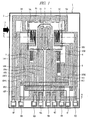
FIG. 1 is a plan view of main parts illustrating an example of a thermal fluid flow sensor according to a first embodiment of the present invention; -
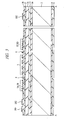
FIG 2 is a plan view of main parts illustrating a manufacturing process of the thermal fluid flow sensor according to the first embodiment of the present invention; -
FIG 3 is a cross-sectional view of main parts illustrating the thermal fluid flow sensor in the manufacturing process continued fromFIG 2 ; -
FIG 4 is a cross-sectional view of main parts illustrating the thermal fluid flow sensor in the manufacturing process continued fromFIG 3 ; -
FIG 5 is a cross-sectional view of main parts illustrating the thermal fluid flow sensor in the manufacturing process continued fromFIG 4 ; -
FIG 6 is a cross-sectional view of main parts illustrating the thermal fluid flow sensor in the manufacturing process continued fromFIG 5 ; -
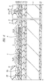
FIG 7 is a cross-sectional view of main parts illustrating the thermal fluid flow sensor in the manufacturing process continued fromFIG 6 ; -
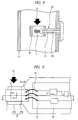
FIG 8 is a schematic layout diagram illustrating a thermal fluid flow meter attached to an air intake path of an internal-combustion engine of, e.g., a vehicle, the thermal fluid flow meter having the thermal fluid flow sensor of the first embodiment of the present invention mounted thereto; -
FIG. 9 is a plan view of main parts illustrating a part ofFIG 8 in an enlarged manner; -
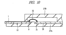
FIG 10 is a cross-sectional view of main parts taken along the line B-B ofFIG 9 ; -
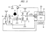
FIG 11 is a circuit diagram illustrating an example of the thermal fluid flow sensor according to the first embodiment of the present invention; -
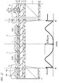
FIG 12 is an explanatory diagram illustrating a shift amount of a surface of a thermal fluid flow sensor which has been compared to the thermal fluid flow sensor according to the first embodiment of the present invention and studied by the inventor of the present invention; -
FIG. 13 is an explanatory diagram illustrating a shift amount of a surface of the thermal fluid flow sensor according to the first embodiment of the present invention; -
FIG 14 is an explanatory diagram illustrating a relation between a wiring pitch and a shift amount of surfaces of the thermal fluid flow sensors; -
FIG 15 is an explanatory diagram illustrating a relation between a total energizing time and a resistance change rate; and -
FIG 16 is a cross-sectional view of main parts of a thermal fluid flow sensor according to a second embodiment of the present invention. - In the embodiments described below, the invention will be described in a plurality of sections or embodiments when required as a matter of convenience. However, these sections or embodiments are not irrelevant to each other unless otherwise stated, and the one relates to the entire or a part of the other as a modification example, details, or a supplementary explanation thereof.
- Also, in the embodiments described below, when referring to the number of elements (including number of pieces, values, amount, range, and the like), the number of the elements is not limited to a specific number unless otherwise stated or except the case where the number is apparently limited to a specific number in principle. The number larger or smaller than the specified number is also applicable.
- Further, in the embodiments described below, it goes without saying that the components (including element steps) are not always indispensable unless otherwise stated or except the case where the components are apparently indispensable in principle. Also, it is needless to say that the expression "(be) formed of an element A" or "comprising an element A" or the like used for describing the components in the embodiments does not limit the element to the cited one(s) unless otherwise stated that the element is limited to the cited one(s).
- Similarly, in the embodiments described below, when the shape of the components, positional relation thereof, and the like are mentioned, the substantially approximate and similar shapes and the like are included therein unless otherwise stated or except the case where it is conceivable that they are apparently excluded in principle. The same goes for the numerical value and the range described above.
- Also, regarding material etc., specified material is main material and thus do not eliminate secondary elements, additives, and added components unless otherwise stated that the specified material is not a main one or the specified material is not a main one in principle or in the situation.
- Also, components having the same function are denoted by the same reference symbols throughout the drawings for describing the embodiments, and the repetitive description thereof is omitted.
- Also, in some drawings used in the embodiments, hatching is used even in a plan view so as to make the drawings easy to see.
- Hereinafter, the embodiments of the present invention will be described in detail with reference to the drawings.
- A plan view of main parts of an example of a thermal fluid flow sensor according to a first embodiment is illustrated in
FIG. 1 . - A
measuring element 1 which is the thermal fluid flow sensor of the first embodiment is composed of asemiconductor substrate 2, a heaterresistive element 3, a temperature-measuring resistive element for heaterresistive element 4, a temperature-measuring resistive element, an air-temperature-measuringresistive element 6, heater-temperature-controllingresistive elements terminal electrodes 9A to 9I, and draw-outwirings 10A, 10B, 10C1,10C2, 10D, 10E, 10F, 10G, 10H1, 10H2, 10I1, and 10I2, etc. - The
semiconductor substrate 2 is formed of, for example, single crystal silicon (Si). - The heater
resistive element 3 is formed on thesemiconductor substrate 2 interposing an insulating film, and has a wiring width of, for example, about 1 to 150 µm. - The temperature-measuring resistive element for heater
resistive element 4 is used for detecting temperature of the heaterresistive element 3, and has a wiring width of, for example, about 0.5 to 100 µm. - The temperature-measuring resistive element is composed of two upstream temperature-measuring
resistive elements resistive elements resistive element 3. Wiring widths of the upstream temperature-measuringresistive elements resistive elements - The air-temperature-measuring
resistive element 6 is used for measuring the air temperature, and has a wiring width of, for example, about 0.5 to 10 µm. - Wiring widths of the heater-temperature-controlling
resistive elements - The
terminal electrodes 9A to 9I are used for connecting signals of the temperature-measuringelement 1 to an external circuit(s). - The draw-out wiring 10A electrically connects the heater
resistive element 3 to theterminal electrode 9A, and has a wiring width of, for example, about 30 to 500 µm. - The draw-out
wiring 10B electrically connects the heaterresistive element 3 to theterminal electrode 9B, and has a wiring width of, for example, about 30 to 500 µm. - The two draw-out wirings 10C1 and 10C2 (mainly, the draw-out wiring 10C1) electrically connect the heater-temperature-controlling
resistive element 7 and the heater-temperature-controllingresistive element 8 to theterminal electrode 9C, and have wiring widths of, for example, about 30 to 500 µm. - The draw-out
wiring 10D electrically connects the temperature-measuring resistive element for heaterresistive element 4 and the heater-temperature-controllingresistive element 7 to theterminal electrode 9D, and has a wiring width of, for example, about 30 to 500 µm. - The draw-out
wiring 10E electrically connects the air-temperature-measuringresistive element 6 and the heater-temperature-controllingresistive element 8 to theterminal electrode 9E, and has a wiring width of, for example, about 30 to 500 µm. - The draw-out
wiring 10F electrically connects the upstream temperature-measuringresistive element 5A and the downstream temperature-measuringresistive element 5C to theterminal electrode 9F, and has a wiring width of, for example, about 30 to 500 µm. - The draw-out
wiring 10G electrically connects the temperature-measuring resistive element for heaterresistive element 4, the air-temperature-measuringresistive element 6, the upstream temperature-measuringresistive element 5B, and the downstream temperature-measuringresistive element 5D to theterminal electrode 9G, and has a wiring width of, for example, about 30 to 500 µm. - The two draw-out wirings 10H1 and 10H2 electrically connect the upstream temperature-measuring
resistive element 5B, and the downstream temperature-measuringresistive element 5C to theterminal electrode 9H, and have wiring widths of, for example, about 30 to 500 µm. - The two draw-out wirings 10I1 and 10I2 electrically connect the upstream temperature-measuring
resistive element 5A and the downstream temperature-measuringresistive element 5D to the terminal electrode 9I, and have wiring widths of, for example, about 30 to 500 µm. - Further, an
opening 11 is provided to at least the heaterresistive element 3, the temperature-measuring resistive element for heaterresistive element 4, and a protective film provided on the temperature-measuring resistive element, and the Si substrate at the lower layer (semiconductor substrate 2) of theopening 11 is removed to have adiaphragm structure 12. Here, according to thediaphragm structure 12, an outer circumference of theopening 11 of the protective film is positioned inside of an outer circumference of thediaphragm structure 12 by more than or equal to 50 µm in the plane. - The measuring
element 1 measures the air temperature of anair flow 13 by the air-temperature-measuringresistive element 6, and calculates a temperature difference (ΔTh) by comparing the measured air temperature with a resistance increase of the temperature-measuring resistive element for heaterresistive element 4 heated by the heaterresistive element 3, and resistances of the temperature-measuringresistive elements resistive element 3. Note that, in the first embodiment, the wiring structure is in a loopback meandering pattern to match the resistance values of the respective resistive elements and setting values. - Next, an example of a method of manufacturing the thermal fluid flow sensor according to the first embodiment will be described in sequence with reference to
FIGS. 2 to 7 . - First, as illustrated in
FIG 2 , thesemiconductor substrate 2 formed of single crystal silicon (Si) is prepared. Subsequently, a first insulatingfilm 14 is formed on a main surface of thesemiconductor substrate 2, and further, a second insulatingfilm 15, a third insulatingfilm 16, a fourth insulatingfilm 17, and a fifth insulatingfilm 18 are sequentially formed. The first insulatingfilm 14 is, for example, a silicon oxide film formed in a furnace body at a high temperature, and has a thickness of about 200 nm. The second insulatingfilm 15 is, for example, a silicon nitride film formed by using a CVD method, and has a thickness of about 100 to 200 nm. The first insulatingfilm 14 and the second insulatingfilm 15 are formed on a back surface of thesemiconductor 2 also. The thirdinsulating film 16 is a silicon oxide film formed by using a CVD method, and has a thickness of about 500 nm. The fourth insulatingfilm 17 is a silicon nitride film formed by using a CVD method similarly to the second insulatingfilm 15 or a silicon nitride film formed by using a plasma CVD method, and has a thickness in a range of about 20 to 200 nm as determined by the wiring pitch of the sensor portion. The fifth insulatingfilm 18 is a silicon oxide film formed by, for example, a CVD method or a plasma CVD method, and has a thickness of 100 to 300 nm. Note that the first insulatingfilm 14, the third insulatingfilm 16, and the fifth insulatingfilm 18 are films (second film) having compressive stress with remnant stress of about 50 to 250 MPa, and the second insulatingfilm 15 and the fourth insulatingfilm 17 are films (first film) having tensile stress of 700 to 1200 MPa. Also, the second insulatingfilm 15 and the fourth insulatingfilm 17 can be aluminum nitride films having tensile stress of 500 to 1200 MPa. - Next, as a
first metal film 19, a Mo (molybdenum) film is formed by, for example, sputtering to be about 150 nm. Here, to improve adhesiveness and crystalline quality, the fifth insulatingfilm 18 which is a base of thefirst metal film 19 is etched by 5 nm to 20 nm by sputtering etching using argon (Ar) gas before depositing the Mo film, and a temperature of thesemiconductor substrate 2 upon depositing the Mo film is set at about 200 to 500°C. Also, to further improve the crystalline quality of the Mo film, a thermal treatment at about 1000°C in a nitride atmosphere is performed in a furnace body or a lamp heating apparatus. - Next, as illustrated in
FIG 3 , thefirst metal film 19 is patterned by etching using photolithography to form the heaterresistive element 3, the temperature-measuring resistive element for heaterresistive element 4, the temperature-measuring resistive element (the upstream temperature-measuringresistive elements resistive elements resistive element 6, the heater-temperature-controllingresistive elements first metal film 19 is over-etched in the processing, the fifth insulatingfilm 18 that is the base is etched by about 50 nm in regions where thefirst metal film 19 is not formed. Therefore, a step between the portion formed of thefirst metal film 19 such as the heaterresistive element 3 and the portion formed of the fifth insulatingfilm 18 formed by processing thefirst metal film 19 is about 200 nm in total. - Next, as illustrated in
FIG. 4 , a sixth insulatingfilm 20, a seventh insulatingfilm 21, and an eighth insulatingfilm 22 are sequentially formed at the upper layer of the heaterresistive element 3, the temperature-measuring resistive element for heaterresistive element 4, the temperature-measuring resistive element 5 (the upstream temperature-measuringresistive elements resistive elements resistive element 6, the heater-temperature-controllingresistive elements film 20 is a silicon oxide film deposited by, for example, a CVD method or a low-temperature CVD method using plasma with TEOS as a source, and has a thickness of about 500 nm. The seventh insulatingfilm 21 is a silicon nitride film deposited by, for example, a CVD method or a low-temperature CVD method using plasma, and has a thickness of about 150 to 200 nm. The eighth insulatingfilm 22 is a silicon oxide film deposited by, for example, a CVD method or a low-temperature CVD method using plasma with TEOS as a source, and has a thickness of about 100 to 500 nm. Note that the sixth insulatingfilm 20 and the eighth insulatingfilm 22 being silicon oxide films are films (second film) having compressive stress with remnant stress at the room temperature of about 50 to 250 MPa, and the seventh insulatingfilm 21 being a silicon nitride film is a film (first film) having tensile stress with remnant stress at the room temperature of about 700 MPa to 1200 MPa. The reason of making the remnant stress (tensile stress) of the seventh insulatingfilm 21 larger than the total remnant stress (compressive stress) of the sixth insulatingfilm 20 and the eighth insulatingfilm 22 in this manner is to prevent deflection of these insulating films to be caused when the temperature of actually using the thermal fluid flow sensor exceeds the temperature of forming these insulating films, making the total remnant stress of the sixth insulatingfilm 20 and the eighth insulatingfilm 22 be larger than the remnant stress of the seventh insulatingfilm 21. Also, when the seventh insulatingfilm 21 is formed of a silicon nitride film formed by a low-temperature CVD using plasma, the condition is adjusted to obtain desired tensile stress by performing a thermal treatment at 800°C or higher, preferably, about 1000°C. As to the silicon oxide films as the sixth insulatingfilm 20 and the eighth insulatingfilm 22, it is preferable to perform a thermal treatment after depositing the silicon oxide films because a thermal treatment at about 1000°C improves the humidity resistance. - Next, as illustrated in
FIG. 5 , aconnection hole 23 which exposes a part of the draw-out wirings 10A to 10I2 is formed by dry etching or wet etching using a photolithography method. Incidentally, inFIG 5 , other connection holes 23 than theconnection hole 23 reaching the draw-outwiring 10G are not illustrated. Then, as asecond metal film 24, an Al (aluminum) alloy film of about 1 µm thick is deposited to bury theconnection hole 23. Note that the surface of the draw-out wirings 10A to 10I2 can be subjected to sputtering etching by Ar (argon) gas before forming thesecond metal film 24 to make the contact between thesecond metal film 24 and the draw-outwiring 10G better. Further, to make the contact surer, a barrier metal film of, for example, a TiN (titanium nitride) film can be formed as a third metal film before depositing the Al alloy film to form a stacked film of the barrier metal film and the Al alloy film. Note that the contact resistance is increased when the barrier metal film is formed to be relatively thick, the thickness of the barrier metal film is preferable to be about 20 nm. Meanwhile, if the problem of increasing resistance can be avoided as an efficient contact area is ensured, the thickness of the barrier metal film can be smaller than or equal to 200 nm. Also, while the TiN film has been exemplified as the barrier metal film, a TiW (titanium tungsten) film, a Ti (titanium) film, or a stacked film of a TiW film and a Ti film can be used. - Next, as illustrated in
FIG 6 , thesecond metal film 24 is patterned by dry etching or wet etching using a photolithography method to form theterminal electrodes 9A to 9I. Next, as aprotective film 25 on theterminal electrodes 9A to 91, e.g., a polyimide film is formed, and theopening 11 and an opening (not illustrated) for connecting theterminal electrodes 9A to 9I and the external circuit(s) are formed on at least the heaterresistive element 3, the temperature-measuring resistive element for heaterresistive element 4, the upstream temperature-measuringresistive elements resistive elements protective film 25 can be a photo-sensitive organic film having a thickness of 2 to 3µm. - Next, as illustrated in
FIG 7 , a pattern (not illustrated) of a photoresist film is formed on the back surface of thesemiconductor substrate 2 by a photolithography method, and the first insulatingfilm 14 and the second insulatingfilm 15 formed on the back surface are removed by dry etching or wet etching. Then, thesemiconductor substrate 2 is subjected to wet etching from the back surface in KOH (potassium hydroxide), TMAH (Tetramethylammonium hydroxide), or a solution containing KOH and/or TMAH using the remained part of the first insulatingfilm 14 and the second insulatingfilm 15 as a mask so that thediaphragm structure 12 is formed. Thediaphragm structure 12 is designed to be larger than theopening 11 of theprotective film 25, more preferably, is formed to be larger than every side lines of theopening 11 of theprotective film 25 by 50 µm or more. The total thickness of the insulating films (the first insulatingfilm 14, second insulatingfilm 15, third insulatingfilm 16, fourth insulatingfilm 17, fifth insulatingfilm 18, sixth insulatingfilm 20, seventh insulatingfilm 21, and eighth insulating film 22) configured in thediaphragm structure 12 is preferably larger than or equal to 1.5 µm. When the total thickness is thinner than 1.5 µm, the strength of the insulating films configured in thediaphragm structure 12 is lowered, and a fear of destroying the structure by collision of dusts contained in the intake air of a vehicle is increased. However, the first insulatingfilm 14 plays a role of a buffering film against dust collision from below. If the configuration is designed not to have dust collision, the first insulatingfilm 14 can be omitted. - Note that, in the present embodiment described in the foregoing, while a thermal fluid flow sensor in which the
first metal film 19 to be the heaterresistive element 3 etc. is formed of Mo has been described, thefirst metal film 19 can be formed of other materials such as a metal other than Mo, a metal nitride compound, a metal silicide compound, polycrystalline silicon, or polycrystalline silicon in which phosphorus or boron is doped as an impurity. When a metal is used, a metal containing, for example, α-Ta (alpha tantalum), Ti (titanium), W (tungsten), Co (cobalt), Ni (nickel), Fe (iron), Nb (niobium), Hf (hafnium), Cr (chrome), Zr (zirconium), or the like as its main component can be exemplified. When a metal nitride compound is used, TaN (tantalum nitride), MoN (molybdenum nitride), WN (tungsten nitride), or the like can be exemplified. When a metal silicide compound is used, MoSi (molybdenum silicide), CoSi (cobalt silicide), NiSi (nickel silicide), or the like can be exemplified. - Also, while breakage of the
diaphragm structure 12 due to water pressure in a chip-dicing process after completing processes to thesemiconductor substrate 2 in a wafer state is considered, there is no problem in the strength when the total film thickness of the stacked insulating film (the first insulatingfilm 14, second insulatingfilm 15, third insulatingfilm 16, fourth insulatingfilm 17, fifth insulatingfilm 18, sixth insulatingfilm 20, seventh insulatingfilm 21, and eighth insulating film 22) configured in thediaphragm structure 12 is larger than or equal to 1.5 µm. -
FIG 8 is a schematic layout diagram of a thermal fluid flow meter attached to an air intake path of an internal-combustion engine of a vehicle or the like, on which the thermal fluid flow sensor according to the first embodiment is mounted. A thermalfluid flow meter 26 is formed of the measuringelement 1 described above that is the thermal fluid flow sensor, a supportingmember 27 having an upper portion and a lower portion, and anexternal circuit 28, the measuringelement 1 being arranged in a by-path 30 provided inside anair path 29. Theexternal circuit 28 is electrically connected to the terminals of the measuringelement 1 via the supportingmember 27. The taken-in air flows in a direction of an air flow illustrated by the arrow (air flow 13) inFIG 8 or a direction opposite to that. -
FIG 9 is a plan view of main parts illustrating a part ofFIG 8 described above (the measuringelement 1 and the supporting member 27) in an enlarged manner.FIG 10 is a cross-sectional view of main parts taken along the line B-B ofFIG 9 . - As illustrated in
FIGS. 9 and10 , the measuringelement 1 is fixed on the supportingmember 27A at the lower portion, and each of theterminal electrodes 9A to 9I of the measuringelement 1 andterminal electrode 31 of theexternal circuit 28 are electrically connected by a wire-bonding method using, for example, agold wire 32 or the like. Theterminal electrodes 9A to 91 and thegold wires 32 are protected as being covered by the supportingmember 27B at the upper portion. The upper portion of the supportingmember 27B can be a sealing protection by a resin. - Next, with reference to
FIG. 11 , an operation of the thermalfluid flow meter 26 described above will be described.FIG. 11 is a circuit diagram illustrating the measuringelement 1 according to the first embodiment and theexternal circuit 28, in which thereference numeral 33 denotes a power source, thereference numeral 34 denotes a transistor for flowing a heating current to the heaterresistive element 3, thereference numeral 35 denotes a control circuit configured by an output circuit including an A/D converter and the like and a CPU (central processing unit) performing arithmetic processing, and thereference numeral 36 denotes a memory circuit. - The circuit illustrated in
FIG 11 has two bridge circuits, one of them is a heater-controlling bridge circuit composed of the temperature-measuring resistive element for heaterresistive element 4, the air-temperature-measuringresistive element 6, and the heater-temperature-controllingresistive elements resistive elements resistive elements - In the measuring
element 1 illustrated inFIG 1 , theterminal electrode 9C is electrically connected to both of the two heater-temperature-controllingresistive elements terminal electrode 9C. Also, theterminal electrode 9F is electrically connected to both of the upstream temperature-measuringresistive element 5A and the downstream temperature-measuringresistive element 5C, and a predetermined potential Vref2 is supplied to theterminal electrode 9F. Further, theterminal electrode 9G is electrically connected to the air-temperature-measuringresistive element 6, the temperature-measuring resistive element for heaterresistive element 4, the upstream temperature-measuringresistive element 5B, and the downstream temperature-measuringresistive element 5D, respectively, via the draw-outwiring 10G, and theterminal electrode 9G is at a ground potential as illustrated inFIG 11 . - The
terminal electrode 9D electrically connected to both of the temperature-measuring resistive element for heaterresistive element 4 and the heater-temperature-controllingresistive element 7 via the draw-outwiring 10D corresponds to a node A inFIG 11 . - Also, the
terminal electrode 9E electrically connected to both of the air-temperature-measuringresistive element 6 and the heater-temperature-controllingresistive element 8 via the draw-outwiring 10E corresponds to a node B inFIG 11 . Further, the terminal electrode 9I electrically connected to both of the upstream temperature-measuringresistive element 5A and the downstream temperature-measuringresistive element 5D via the two draw-out wirings 10I1 and 10I2 corresponds to a node C inFIG 11 . Moreover, theterminal electrode 9H electrically connected to both of the upstream temperature-measuringresistive element 5B and the downstream temperature-measuringresistive element 5C via the two draw-out wirings 10H1 and 10H2 corresponds to a node D inFIG 11 . - Note that, while the ground potential of the heater-controlling bridge circuit and the temperature-sensor bridge circuit is supplied to the
common terminal electrode 9G in the present embodiment, the number of terminal electrodes can be increased to make each of the terminal electrodes to be the ground potential. - In the heater-controlling bridge circuit, respective resistance values of the temperature-measuring resistive element for heater
resistive element 4, the air-temperature-measuringresistive element 6, and the heater-temperature-controllingresistive elements terminal electrode 9D) and the node B (terminal electrode 9E) to be 0 V when a gas heated by the heaterresistive element 3 is at a temperature higher than the intake air temperature by a fixed temperature (ΔTh, e.g., 100°C). When the above-mentioned fixed temperature (ΔTh) is shifted from the setting value, a potential difference is generated between the node A and the node B. The heater-controlling bridge circuit is designed to change the current in the heaterresistive element 3 with controlling thetransistor 34 by thecontrol circuit 35, so that the bridge circuit is maintained at an equilibrium state (potential difference between A and B is 0 V). - On the other hand, since the temperature-sensor bridge circuit is designed to have distances between the heater
resistive element 3 to the respective temperature-measuring resistive elements (the upstream temperature-measuringresistive elements resistive elements terminal electrode 9H) is in an equilibrium state to be 0 V regardless of heating by the heaterresistive element 3. When a voltage is applied to the heaterresistive element 3 and the intake air flows in the direction of theair flow 13, the temperature of the upstream temperature-measuringresistive elements resistive element 3 is lowered and the temperature of the downstream temperature-measuringresistive elements control circuit 35, and an air flow rate (Q) obtained by a comparison table of the voltage difference and the air flow rate recorded in thememory circuit 36 is arithmetically processed and outputted. Note that, even when theair flow 13 is in the opposite direction, the air flow rate can be measured in the same manner. Therefore, a reverse-flow detection is also possible. - Next, a shift amount of a diaphragm surface will be described.
FIG. 12 is a cross-sectional view of main parts a thermal fluid flow sensor of a conventional system having a diaphragm structure, the sensor having been compared with the diaphragm structure 12 (seeFIG 7 ) of the present invention and studied by the inventor of the present invention. In plane,FIG. 12 corresponds to the line A-A inFIG 1 of the first embodiment. In addition, in the conventional thermal fluid flow sensor, a pitch of sensor wirings (the upstream temperature-measuringresistive elements resistive elements FIG 12 . - As illustrated in
FIG 12 , the conventional thermal fluid flow sensor has a structure in which the fourth insulatingfilm 17 formed of a silicon nitride film and the fifth insulatingfilm 18 formed of a silicon oxide film of the thermal fluid flow sensor of the present embodiment are omitted. In the configuration of films, a silicon oxide film (the first insulating film 14) formed on thesemiconductor substrate 2 by a thermal treatment is about 200 nm, a silicon nitride film (the second insulating film 15) formed by a CVD method is about 200 nm, a silicon oxide film (the third insulating film 16) deposited by a CVD method is about 500 nm, a Mo film (the heaterresistive element 3, the temperature-measuring resistive element for heaterresistive element 4, the temperature-measuring resistive element (the upstream temperature-measuringresistive elements resistive elements resistive element 6, the heater-temperature-controllingresistive elements protective film 25, and the diaphragm structure is formed in which thesemiconductor substrate 2 is removed in the region larger than the portions of the heater, the heater temperature sensor, and the temperature difference sensor. - In the structure of the conventional thermal fluid flow sensor as described above, the surface is deflected in the sensor portion (the upstream temperature-measuring
resistive elements resistive elements protective film 25. As the heater portion (the heater resistive element 3) at the center and the sensor portion (the upstream temperature-measuringresistive elements resistive elements resistive element 3, the temperature-measuring resistive element for heaterresistive element 4, and the temperature-measuring element (the upstream temperature-measuringresistive elements resistive elements - On the other hand,
FIG 13 illustrates a shift amount of the surface of the thermal fluid flow sensor of the present embodiment with setting the pitch of the sensor wirings (the upstream temperature-measuringresistive elements resistive elements - In the configuration of each film forming the thermal fluid flow sensor of the present embodiment, a silicon oxide film (the first insulating film 14) formed on the semiconductor substrate 2 by a thermal treatment is about 200 nm, a silicon nitride film (the second insulating film 15) formed by a CVD method is about 200 nm, a silicon oxide film (the third insulating film 16) deposited by a CVD method is about 350 nm, a silicon nitride film (the fourth insulating film 17) for compensating the tensile stress of the silicon nitride film above is about 140 nm, a silicon oxide film (the fifth insulating film 18) above the silicon nitride film is about 150 nm, a Mo film (the heater resistive element 3, the temperature-measuring resistive element for heater resistive element 4, the temperature-measuring resistive element (the upstream temperature-measuring resistive elements 5A and 5B and the downstream temperature-measuring resistive elements 5C and 5D), the air-temperature-measuring resistive element 6, the heater-temperature-controlling resistive elements 7 and 8, and the draw-out wirings 10A to 10I2) patterned on the silicon oxide film is about 150 nm, a silicon oxide film (the sixth insulating film 20) deposited by a plasma CVD method using TEOS as a source is about 500 nm, a silicon nitride film (the seventh insulating film 21) deposited by a plasma CVD method is about 150 nm, and a silicon oxide film (the eighth insulating film 22) deposited by a plasma CVD method using TEOS as a source is about 200 nm. To the portions other than the heater, heater temperature sensor, and the temperature difference sensor, a polyimide film is formed to be about 2 µm as the
protective film 25, and the diaphragm structure is formed in which thesemiconductor substrate 2 is removed in the region larger than the portions of the heater, heater temperature sensor, and the temperature difference sensor. - In such a diaphragm structure of the thermal fluid flow sensor of the present embodiment, the shift amount of the surface can be about only 0.1 µm when comparing the heater portion and the sensor portion at the center, the shift amount being reduced to be about 1/28 (one-twenty-eighth) of the shift amount in the conventional thermal fluid flow sensor. In other words, the deflection occurring in the diaphragm structure can be largely reduced, thereby preventing changes in the resistance values of the heater portion and the sensor portion, and preventing malfunctions such as a lowering in the detection accuracy due to a lowering of ΔTh and/or destruction of the film structure body due to abnormal heating caused by an excess current.
-
FIG 14 is a diagram illustrating a correlation of the pitch of the sensor wirings (the upstream temperature-measuringresistive elements resistive elements FIG 14 , the horizontal axis is the pitch of the sensor wirings and the vertical axis is the shift amount of the surface of the diaphragm structure. - As illustrated in
FIG 14 , in the conventional thermal fluid flow sensor, the shift amount of the surface of the diaphragm structure portion is increased when the wiring pitch is smaller than or equal to about 6 nm, more particularly, the shift amount is drastically increased when the wiring pitch is smaller than or equal to about 1.2 µm. Meanwhile, in the thermal fluid flow sensor of the present embodiment, the shift amount of the surface of the diaphragm structure is about 0.1 µm even when the wiring pitch is as minute as 1.2 µm. Thus, it is understood that an imbalance of stress in the insulating film in the diaphragm structure is resolved in the present embodiment. Note that, in the present embodiment, as compared with the conventional system, the silicon nitride film (the fourth insulating film 17) having a thickness of about 140 nm is added at a lower layer of the wiring layer formed of the first metal film 19 (seeFIG 2 ) corresponding to the wiring pitch set to about 1.2 µm. By setting the thickness of the silicon nitride film corresponding to the wiring pitch, the shift amount of the surface of the diaphragm structure can be reduced. - Also, in the present embodiment, it has been described that the tensile stress of the silicon nitride film (the seventh insulating film 21) formed of the first metal film 19 (see
FIG 2 ) on the wiring has remnant stress of about 700 MPa to 1000 MPa. Meanwhile, as the silicon nitride film on the wiring plays a large role of preventing moisture absorption, the remnant stress may not be within the above-mentioned range. However, when the remnant stress is not within the range, it is necessary to add a silicon nitride film in consideration of the whole remnant stress at a lower layer of the wiring, and the number of layers of the silicon nitride film to be formed at the lower layer of the wiring can be three or more when a film having compressive stress (e.g., a silicon oxide film) is interposed therebetween. Also, the remnant stress may be compressive stress depending on the temperature upon deposition even in a silicon nitride film. Thus, depending on the temperature in the environment of using the thermal fluid flow sensor, the remnant stress is changed from tensile stress to compressive stress and vice versa even in the same film. Therefore, selection of the number of layers of these silicon nitride films and the silicon oxide films and/or the species of the films themselves can be suitably set depending on the environment of using the thermal fluid flow sensor. -
FIG.15 illustrates a resistance change rate of the heater portion per total energizing time when the heater portion (the heater resistive element 3) is energized to be 500°C. InFIG. 15 , the conventional thermal fluid flow sensor (seeFIG 12 ) and the thermal fluid flow sensor of the present embodiment (seeFIG 13 ) are compared in conditions of having the pitch of the sensor wirings (the upstream temperature-measuringresistive elements resistive elements - As illustrated in
FIG. 15 , in the conventional thermal fluid flow sensor, the surface of the sensor portion is deflected like a convex and thus the resistance value of the heater portion is drastically changed even though the surface of the heater portion is in almost the same plane with the uppermost silicon oxide film (the eighth insulating film 22) (see FIG 22 also). On the other hand, in the thermal fluid flow sensor of the present embodiment, about a 0.5% resistance value change was observed in the initial period of energization but there is no change observed in the resistance value thereafter. Note that, also as to the heater temperature sensor (the temperature-measuring resistive element for heater resistive element 4) in a condition of energizing the heater portion at about 500°C, it has been confirmed that the conventional thermal fluid flow sensor has a large resistance value change, and the thermal fluid flow sensor of the present embodiment has almost no resistance value change. Therefore, by making the shift amount of the surface between the sensor portion and the heater portion small, a thermal fluid flow sensor having a high reliability can be achieved. - Note that, in the conventional thermal fluid flow sensor, means of ensuring the tensile stress of the diaphragm structure by simply thickening the silicon nitride film (the second insulating film 15) at a lower layer of the Mo film (the first metal film 19) may be considered. However, since the silicon nitride film has very large remnant stress of 700 MPa to 1000 MPa, warpage of the wafer (the semiconductor substrate 2) is increased when the thickness exceeds 200 nm. Therefore, it is feared that an error in chucking wafers in an apparatus is posed in the upcoming processes after forming the silicon nitride film (the second insulating film 15), and thus adverse effects such as cracks in the silicon nitride film, exfoliation of the film, and/or wafer cracking are/is feared to occur.
- In the above point of view also, as described in the present embodiment, the film having tensile stress is stacked by two layers or more to have a thickness smaller than or equal to 200 nm, and it is preferable to interpose a film having compressive stress between the tensile stress films instead of sequentially stacking the tensile stress films in view of mitigating inertial stress. Consequently, thermal stress resistance can be improved.
- Further, since the thickness of the whole diaphragm structure becomes thicker by the added silicon nitride film, the mechanical strength is increased, thereby improving the dust collision resistance.
- In a second embodiment, prevention of warpage of a wafer due to remnant stress which a film deposited on the wafer (the semiconductor substrate 2) has is considered.
-
FIG 16 illustrates an example of a thermal fluid flow sensor according to the second embodiment, illustrating a cross-sectional view of main parts taken along the line A-A inFIG 1 of the first embodiment. - Thicknesses of respective films configuring the thermal fluid flow sensor of the second embodiment are the same with those of the first embodiment except for the fourth insulating film 17 (a silicon nitride film) having a thickness of about 200 nm (it has been about 140 nm in the first embodiment).
- Next, a manufacturing process of the thermal fluid flow sensor according to the second embodiment will be described. Note that the manufacturing process of the thermal fluid flow sensor of the second embodiment is the same with that of the first embodiment until the step of depositing the fourth insulating film 17 (see
FIG 2 ). - Subsequently, the fourth insulating
film 17 is processed with dry etching using a photoresist pattern patterned by a photolithography method as a mask or the like. In the processing, the fourth insulatingfilm 17 is arranged to cover at least the region of the wiring portion in the diaphragm in plane, and spacing L between the outer circumference of the fourth insulatingfilm 17 and the outer circumference of thediaphragm structure 12 is preferably larger than or equal to 10 µm. By the patterning, the fourth insulatingfilm 17 formed of a silicon nitride film is remained only inside thediaphragm structure 12, so that warpage of the wafer (the semiconductor substrate 2) due to strong tensile stress of the fourth insulatingfilm 17 is mitigated, and thus troubles in wafer transfer in a plasma CVD apparatus which requires electrostatic chucking and/or a stepper apparatus used in a photolithography step which uses vacuum contact can be avoided. - Upcoming steps from the step of depositing the fifth insulating
film 18 are the same with those of the first embodiment. Meanwhile, in the second embodiment, the thickness of the seventh insulating film 21 (silicon nitride film) is about 150 nm to 200 nm, and the thickness of the eighth insulating film 22 (silicon oxide film) is about 300 nm. - In the foregoing, the invention made by the inventor of the present invention has been concretely described based on the embodiments. However, it is needless to say that the present invention is not limited to the foregoing embodiments and various modifications and alterations can be made within the scope of the present invention.
- Other than the thermal fluid flow sensor according to the above-described embodiments, the present invention is applicable to various sensors such as an acceleration sensor, a temperature sensor, and a gas sensor.
Claims (14)
- A thermal fluid flow sensor comprising: a heater resistive element provided in a diaphragm structure body and a temperature-measuring resistive element provided next to the heater resistive element, the thermal fluid flow sensor measuring an air flow rate, wherein
an insulating film formed by stacking a first film having tensile stress and a second film having compressive stress is provided to an upper layer and a lower layer of the heater resistive element and the temperature-measuring resistive element, and
at least the insulating film at the lower layer of the temperature-measuring resistive element has the first film and the second film being alternately formed, and the number of the first film is two or more. - The thermal fluid flow sensor according to claim 1, wherein
the first film is a silicon nitride film or an aluminum nitride film having tensile stress with remnant stress at the room temperature of 700 MPa or more. - The thermal fluid flow sensor according to claim 1, wherein
the second film is a silicon oxide film or a film containing silicon oxide as its main component formed by a plasma CVD method using TEOS (tetraethyl orthosilicate) as a source having compressive stress with remnant stress at the room temperature of 300 MPa or lower. - The thermal fluid flow sensor according to claim 1, wherein
the insulating film at the lower layer of the heater resistive element has a five-layer structure having two layers of the first films and three layers of the second films, and remnant stress at the room temperature of the insulating film as a whole at the lower layer of the heater resistive element is tensile stress. - The thermal fluid flow sensor according to claim 1, wherein
a wiring pitch of the temperature-measuring resistive element is smaller than or equal to 20 µm. - The thermal fluid flow sensor according to claim 5, wherein
the wiring pitch of the temperature-measuring resistive element is smaller than or equal to 6 µm. - The thermal fluid flow sensor according to claim 1, wherein
the insulating film at the upper layer of the heater resistive element and the temperature-measuring resistive element includes a silicon nitride film for preventing moisture absorption. - The thermal fluid flow sensor according to claim 1, wherein
the number of layers of the silicon nitride films included in the insulating film at the lower layer of the heater resistive element is larger than that of the silicon nitride films included in the insulating film at the upper layer of the heater resistive element. - The thermal fluid flow sensor according to claim 1, wherein
the insulating film at the lower layer of the heater resistive element and the insulating film at the upper layer of the heater resistive element have asymmetric configurations of the films. - The thermal fluid flow sensor according to claim 1, wherein
the diaphragm structure body is configured by the insulating films stacked at the upper layer and the lower layer of the heater resistive element, and a total thickness of the insulating films of the upper layer and the lower layer of the heater resistive element is larger than or equal to 1.5 µm. - The thermal fluid flow sensor according to claim 1, wherein
the heater resistive element and the temperature-measuring resistive element are formed of a metal film, a metal nitride compound, a metal silicide compound, poly-silicon, or doped silicon,
the metal film contains any of molybdenum, alpha-tantalum, titanium, tungsten, cobalt, nickel, iron, niobium, hafnium, chrome, zirconium, platinum, or beta-tantalum as its main component,
the metal nitride compound is any of tantalum nitride, molybdenum nitride, tungsten nitride, or titanium nitride,
the metal silicide compound is any of tungsten silicide, molybdenum silicide, cobalt silicide, or nickel silicide, and
phosphorus or born is doped in the doped silicon. - The thermal fluid flow sensor according to claim 1, wherein
an outer circumference of the first film in plane is a region covering at least a microprocessed wiring portion in a diaphragm, and positioned inside an outer circumference of the diaphragm structure body by more than or equal to 10 µm. - A method of manufacturing a thermal fluid flow sensor, the thermal fluid flow sensor having a heater resistive element provided in a diaphragm structure body and a temperature-measurement resistive element provided next to the heater resistive element and measuring an air flow rate, the method comprising the steps of:(a) stacking a first film having tensile stress and a second film having compressive stress on a semiconductor substrate;(b) patterning the first film;(c) forming the heater resistive element and the temperature-measuring resistive element on the first film and the second film after the step (b); and,(d) as the heater resistive element and the temperature-measuring resistive element being exist, stacking the first film having tensile stress and the second film having compressive stress, the first film and the second film being different from those of the step (a), wherein,
in the step (b), the first film is pattered to have its outer circumference positioned inside an outer circumference of the diaphragm structure body. - The method of manufacturing a thermal fluid flow sensor according to claim 13, wherein
the outer circumference of the first film in plane is positioned inside the outer circumference of the diaphragm structure body by more than or equal to 10 µm.
Applications Claiming Priority (1)
| Application Number | Priority Date | Filing Date | Title |
|---|---|---|---|
| JP2008312359A JP5276964B2 (en) | 2008-12-08 | 2008-12-08 | Thermal fluid flow sensor and manufacturing method thereof |
Publications (2)
| Publication Number | Publication Date |
|---|---|
| EP2204346A1 true EP2204346A1 (en) | 2010-07-07 |
| EP2204346B1 EP2204346B1 (en) | 2017-03-15 |
Family
ID=42084618
Family Applications (1)
| Application Number | Title | Priority Date | Filing Date |
|---|---|---|---|
| EP09015011.1A Active EP2204346B1 (en) | 2008-12-08 | 2009-12-03 | Thermal fluid flow sensor and method of manufacturing the same |
Country Status (4)
| Country | Link |
|---|---|
| US (1) | US8429964B2 (en) |
| EP (1) | EP2204346B1 (en) |
| JP (1) | JP5276964B2 (en) |
| CN (2) | CN102735298B (en) |
Cited By (1)
| Publication number | Priority date | Publication date | Assignee | Title |
|---|---|---|---|---|
| EP2503305A1 (en) * | 2011-03-25 | 2012-09-26 | Hitachi Automotive Systems, Ltd. | Thermal fluid flow sensor and method of manufacturing the same |
Families Citing this family (32)
| Publication number | Priority date | Publication date | Assignee | Title |
|---|---|---|---|---|
| JP5406674B2 (en) | 2009-11-06 | 2014-02-05 | 日立オートモティブシステムズ株式会社 | Thermal fluid flow sensor and manufacturing method thereof |
| JP5542505B2 (en) * | 2010-04-01 | 2014-07-09 | 日立オートモティブシステムズ株式会社 | Thermal flow sensor |
| JP5372976B2 (en) * | 2011-01-31 | 2013-12-18 | 日立オートモティブシステムズ株式会社 | Thermal flow sensor |
| DE102011004782A1 (en) * | 2011-02-25 | 2012-08-30 | Harting Kgaa | Removable micro and nano components for space-saving use |
| JP5982398B2 (en) * | 2011-11-28 | 2016-08-31 | 日立オートモティブシステムズ株式会社 | Thermal air flow sensor |
| JP5753807B2 (en) * | 2012-03-14 | 2015-07-22 | 日立オートモティブシステムズ株式会社 | Thermal fluid flow sensor and manufacturing method thereof |
| US9746361B2 (en) | 2012-04-11 | 2017-08-29 | University Of Virginia Patent Foundation | Gaseous flow sensor and related method thereof |
| CN104364620B (en) * | 2012-06-15 | 2017-07-21 | 日立汽车系统株式会社 | Flow sensor and its manufacture method |
| JP5675716B2 (en) * | 2012-06-29 | 2015-02-25 | 日立オートモティブシステムズ株式会社 | Thermal air flow sensor |
| JP5883740B2 (en) * | 2012-08-01 | 2016-03-15 | 日立オートモティブシステムズ株式会社 | Thermal air flow sensor |
| CN103151253B (en) * | 2013-02-22 | 2015-07-22 | 北京京东方光电科技有限公司 | Method for making signal wire, thin film transistor, array substrate and display device |
| JPWO2015076117A1 (en) | 2013-11-20 | 2017-03-16 | 株式会社村田製作所 | Thermal flow sensor |
| JP6362913B2 (en) * | 2014-04-28 | 2018-07-25 | 日立オートモティブシステムズ株式会社 | Thermal air flow sensor |
| GB201410317D0 (en) * | 2014-06-10 | 2014-07-23 | Spts Technologies Ltd | Substrate |
| JP6438706B2 (en) * | 2014-08-22 | 2018-12-19 | 日立オートモティブシステムズ株式会社 | Sensor device |
| JP6158156B2 (en) * | 2014-09-30 | 2017-07-05 | 日立オートモティブシステムズ株式会社 | Method for manufacturing thermal fluid sensor |
| WO2016084664A1 (en) * | 2014-11-28 | 2016-06-02 | 日立オートモティブシステムズ株式会社 | Thermal-type flow rate sensor |
| JP6295209B2 (en) | 2015-01-09 | 2018-03-14 | 日立オートモティブシステムズ株式会社 | Thermal fluid flow sensor |
| JP6300773B2 (en) * | 2015-10-23 | 2018-03-28 | 三菱電機株式会社 | Semiconductor pressure sensor |
| DE102016206549A1 (en) * | 2016-04-19 | 2017-10-19 | Robert Bosch Gmbh | Sensor element for thermal anemometry |
| CN106898829B (en) * | 2017-03-02 | 2023-11-21 | 华霆(合肥)动力技术有限公司 | Battery system instability detection equipment and method |
| DE102017112611A1 (en) * | 2017-06-08 | 2018-12-13 | Heraeus Noblelight Gmbh | Infrared radiator and method for its manufacture |
| CN108328570A (en) * | 2018-01-31 | 2018-07-27 | 北京航天控制仪器研究所 | A kind of MEMS chip splinter method and supporting tool with film back cavity structure |
| JP6661678B2 (en) * | 2018-02-23 | 2020-03-11 | 三菱電機株式会社 | Thermal detection sensor |
| JP6990165B2 (en) * | 2018-12-05 | 2022-01-12 | 日立Astemo株式会社 | Thermal sensors and their manufacturing methods and semiconductor devices |
| US11268839B2 (en) * | 2019-03-05 | 2022-03-08 | Measurement Specialties, Inc. | Resistive flow sensor |
| JP7163247B2 (en) * | 2019-05-28 | 2022-10-31 | 日立Astemo株式会社 | Thermal sensor and humidity detector for internal combustion engine |
| JP7134920B2 (en) | 2019-06-17 | 2022-09-12 | 日立Astemo株式会社 | Thermal sensor device |
| US11410937B2 (en) * | 2020-03-06 | 2022-08-09 | Raytheon Company | Semiconductor device with aluminum nitride anti-deflection layer |
| JP7112001B2 (en) * | 2020-10-15 | 2022-08-03 | ダイキン工業株式会社 | Thermal velocity/flow sensor and air conditioner |
| CN115752610A (en) * | 2022-11-15 | 2023-03-07 | 苏州敏芯微电子技术股份有限公司 | Thermal flow sensor structure |
| WO2026110272A1 (en) * | 2024-11-21 | 2026-05-28 | Astemo株式会社 | Air flow rate sensing device |
Citations (4)
| Publication number | Priority date | Publication date | Assignee | Title |
|---|---|---|---|---|
| US6240777B1 (en) * | 1997-10-07 | 2001-06-05 | Robert Bosch Gmbh | Sensor having a membrane |
| US6450025B1 (en) * | 1998-03-20 | 2002-09-17 | Denso Corporation | Micro-heater and airflow sensor using the same |
| US20030019290A1 (en) * | 2001-07-27 | 2003-01-30 | Takao Iwaki | Flow sensor |
| US20050186696A1 (en) * | 2002-03-27 | 2005-08-25 | Hitachi, Ltd. | Gas flowmeter and manufacturing method thereof |
Family Cites Families (12)
| Publication number | Priority date | Publication date | Assignee | Title |
|---|---|---|---|---|
| JPH11295127A (en) | 1998-04-06 | 1999-10-29 | Mitsubishi Electric Corp | Flow rate detecting element, flow rate sensor, and method of manufacturing flow rate detecting element |
| DE19951595A1 (en) * | 1999-10-27 | 2001-05-17 | Bosch Gmbh Robert | Mass flow sensor comprises a frame formed partially by silicon, metal layer, heating element, temperature measuring element and a membrane having a dielectric and/or non-conducting accommodating layer |
| JP3468731B2 (en) * | 2000-01-14 | 2003-11-17 | 株式会社日立製作所 | Thermal air flow sensor, element, and internal combustion engine controller |
| JP2002131106A (en) | 2000-10-24 | 2002-05-09 | Hitachi Ltd | Micro heater and thermal air flow meter |
| JPWO2003052355A1 (en) * | 2001-12-14 | 2005-04-28 | 三菱電機株式会社 | Flow sensor |
| JP5108234B2 (en) | 2005-02-07 | 2012-12-26 | 日本特殊陶業株式会社 | Micro heater and sensor |
| US7360416B2 (en) * | 2005-07-07 | 2008-04-22 | Ricoh Company, Ltd. | Non-contact condensation detecting apparatus |
| JP4966526B2 (en) | 2005-09-07 | 2012-07-04 | 日立オートモティブシステムズ株式会社 | Flow sensor |
| JP2007309914A (en) * | 2006-04-20 | 2007-11-29 | Denso Corp | Manufacturing method of physical quantity sensor |
| JP2008170382A (en) * | 2007-01-15 | 2008-07-24 | Hitachi Ltd | Thermal fluid flow sensor and manufacturing method thereof |
| JP5202007B2 (en) | 2008-01-29 | 2013-06-05 | 日立オートモティブシステムズ株式会社 | Thermal fluid flow sensor |
| JP5406674B2 (en) * | 2009-11-06 | 2014-02-05 | 日立オートモティブシステムズ株式会社 | Thermal fluid flow sensor and manufacturing method thereof |
-
2008
- 2008-12-08 JP JP2008312359A patent/JP5276964B2/en active Active
-
2009
- 2009-12-03 EP EP09015011.1A patent/EP2204346B1/en active Active
- 2009-12-08 CN CN201210209399.5A patent/CN102735298B/en active Active
- 2009-12-08 US US12/633,142 patent/US8429964B2/en active Active
- 2009-12-08 CN CN200910253536.3A patent/CN101750123B/en active Active
Patent Citations (4)
| Publication number | Priority date | Publication date | Assignee | Title |
|---|---|---|---|---|
| US6240777B1 (en) * | 1997-10-07 | 2001-06-05 | Robert Bosch Gmbh | Sensor having a membrane |
| US6450025B1 (en) * | 1998-03-20 | 2002-09-17 | Denso Corporation | Micro-heater and airflow sensor using the same |
| US20030019290A1 (en) * | 2001-07-27 | 2003-01-30 | Takao Iwaki | Flow sensor |
| US20050186696A1 (en) * | 2002-03-27 | 2005-08-25 | Hitachi, Ltd. | Gas flowmeter and manufacturing method thereof |
Cited By (1)
| Publication number | Priority date | Publication date | Assignee | Title |
|---|---|---|---|---|
| EP2503305A1 (en) * | 2011-03-25 | 2012-09-26 | Hitachi Automotive Systems, Ltd. | Thermal fluid flow sensor and method of manufacturing the same |
Also Published As
| Publication number | Publication date |
|---|---|
| CN101750123B (en) | 2012-08-15 |
| US20100139391A1 (en) | 2010-06-10 |
| JP5276964B2 (en) | 2013-08-28 |
| CN101750123A (en) | 2010-06-23 |
| CN102735298B (en) | 2015-07-15 |
| JP2010133897A (en) | 2010-06-17 |
| CN102735298A (en) | 2012-10-17 |
| EP2204346B1 (en) | 2017-03-15 |
| US8429964B2 (en) | 2013-04-30 |
Similar Documents
| Publication | Publication Date | Title |
|---|---|---|
| EP2204346B1 (en) | Thermal fluid flow sensor and method of manufacturing the same | |
| US8468883B2 (en) | Thermal type flow sensor having a humidity detection portion and an air flow detecting portion | |
| JP5526065B2 (en) | Thermal sensor and manufacturing method thereof | |
| JP5202007B2 (en) | Thermal fluid flow sensor | |
| EP1762851B1 (en) | Flow sensor with metal film resistor | |
| US20100132452A1 (en) | Thermal type fluid flow sensor and manufacturing method thereof | |
| JP4474771B2 (en) | Flow measuring device | |
| JP5753807B2 (en) | Thermal fluid flow sensor and manufacturing method thereof | |
| JP6532810B2 (en) | Flow sensor | |
| WO2015182257A1 (en) | Flow rate sensor and method for manufacturing same | |
| JP6158156B2 (en) | Method for manufacturing thermal fluid sensor | |
| JP2005181016A (en) | Thermal sensor | |
| WO2003102974A1 (en) | Platinum thin film and thermal sensor |
Legal Events
| Date | Code | Title | Description |
|---|---|---|---|
| PUAI | Public reference made under article 153(3) epc to a published international application that has entered the european phase |
Free format text: ORIGINAL CODE: 0009012 |
|
| 17P | Request for examination filed |
Effective date: 20100331 |
|
| AK | Designated contracting states |
Kind code of ref document: A1 Designated state(s): AT BE BG CH CY CZ DE DK EE ES FI FR GB GR HR HU IE IS IT LI LT LU LV MC MK MT NL NO PL PT RO SE SI SK SM TR |
|
| AX | Request for extension of the european patent |
Extension state: AL BA RS |
|
| 17Q | First examination report despatched |
Effective date: 20160520 |
|
| GRAP | Despatch of communication of intention to grant a patent |
Free format text: ORIGINAL CODE: EPIDOSNIGR1 |
|
| INTG | Intention to grant announced |
Effective date: 20161004 |
|
| STAA | Information on the status of an ep patent application or granted ep patent |
Free format text: STATUS: GRANT OF PATENT IS INTENDED |
|
| GRAS | Grant fee paid |
Free format text: ORIGINAL CODE: EPIDOSNIGR3 |
|
| GRAA | (expected) grant |
Free format text: ORIGINAL CODE: 0009210 |
|
| STAA | Information on the status of an ep patent application or granted ep patent |
Free format text: STATUS: THE PATENT HAS BEEN GRANTED |
|
| AK | Designated contracting states |
Kind code of ref document: B1 Designated state(s): AT BE BG CH CY CZ DE DK EE ES FI FR GB GR HR HU IE IS IT LI LT LU LV MC MK MT NL NO PL PT RO SE SI SK SM TR |
|
| REG | Reference to a national code |
Ref country code: CH Ref legal event code: EP Ref country code: GB Ref legal event code: FG4D |
|
| REG | Reference to a national code |
Ref country code: IE Ref legal event code: FG4D |
|
| REG | Reference to a national code |
Ref country code: AT Ref legal event code: REF Ref document number: 875329 Country of ref document: AT Kind code of ref document: T Effective date: 20170415 |
|
| REG | Reference to a national code |
Ref country code: DE Ref legal event code: R096 Ref document number: 602009044710 Country of ref document: DE |
|
| REG | Reference to a national code |
Ref country code: NL Ref legal event code: MP Effective date: 20170315 |
|
| REG | Reference to a national code |
Ref country code: LT Ref legal event code: MG4D |
|
| PG25 | Lapsed in a contracting state [announced via postgrant information from national office to epo] |
Ref country code: GR Free format text: LAPSE BECAUSE OF FAILURE TO SUBMIT A TRANSLATION OF THE DESCRIPTION OR TO PAY THE FEE WITHIN THE PRESCRIBED TIME-LIMIT Effective date: 20170616 Ref country code: LT Free format text: LAPSE BECAUSE OF FAILURE TO SUBMIT A TRANSLATION OF THE DESCRIPTION OR TO PAY THE FEE WITHIN THE PRESCRIBED TIME-LIMIT Effective date: 20170315 Ref country code: HR Free format text: LAPSE BECAUSE OF FAILURE TO SUBMIT A TRANSLATION OF THE DESCRIPTION OR TO PAY THE FEE WITHIN THE PRESCRIBED TIME-LIMIT Effective date: 20170315 Ref country code: NO Free format text: LAPSE BECAUSE OF FAILURE TO SUBMIT A TRANSLATION OF THE DESCRIPTION OR TO PAY THE FEE WITHIN THE PRESCRIBED TIME-LIMIT Effective date: 20170615 Ref country code: FI Free format text: LAPSE BECAUSE OF FAILURE TO SUBMIT A TRANSLATION OF THE DESCRIPTION OR TO PAY THE FEE WITHIN THE PRESCRIBED TIME-LIMIT Effective date: 20170315 |
|
| REG | Reference to a national code |
Ref country code: AT Ref legal event code: MK05 Ref document number: 875329 Country of ref document: AT Kind code of ref document: T Effective date: 20170315 |
|
| PG25 | Lapsed in a contracting state [announced via postgrant information from national office to epo] |
Ref country code: LV Free format text: LAPSE BECAUSE OF FAILURE TO SUBMIT A TRANSLATION OF THE DESCRIPTION OR TO PAY THE FEE WITHIN THE PRESCRIBED TIME-LIMIT Effective date: 20170315 Ref country code: SE Free format text: LAPSE BECAUSE OF FAILURE TO SUBMIT A TRANSLATION OF THE DESCRIPTION OR TO PAY THE FEE WITHIN THE PRESCRIBED TIME-LIMIT Effective date: 20170315 Ref country code: BG Free format text: LAPSE BECAUSE OF FAILURE TO SUBMIT A TRANSLATION OF THE DESCRIPTION OR TO PAY THE FEE WITHIN THE PRESCRIBED TIME-LIMIT Effective date: 20170615 |
|
| PG25 | Lapsed in a contracting state [announced via postgrant information from national office to epo] |
Ref country code: NL Free format text: LAPSE BECAUSE OF FAILURE TO SUBMIT A TRANSLATION OF THE DESCRIPTION OR TO PAY THE FEE WITHIN THE PRESCRIBED TIME-LIMIT Effective date: 20170315 |
|
| PG25 | Lapsed in a contracting state [announced via postgrant information from national office to epo] |
Ref country code: CZ Free format text: LAPSE BECAUSE OF FAILURE TO SUBMIT A TRANSLATION OF THE DESCRIPTION OR TO PAY THE FEE WITHIN THE PRESCRIBED TIME-LIMIT Effective date: 20170315 Ref country code: SK Free format text: LAPSE BECAUSE OF FAILURE TO SUBMIT A TRANSLATION OF THE DESCRIPTION OR TO PAY THE FEE WITHIN THE PRESCRIBED TIME-LIMIT Effective date: 20170315 Ref country code: ES Free format text: LAPSE BECAUSE OF FAILURE TO SUBMIT A TRANSLATION OF THE DESCRIPTION OR TO PAY THE FEE WITHIN THE PRESCRIBED TIME-LIMIT Effective date: 20170315 Ref country code: IT Free format text: LAPSE BECAUSE OF FAILURE TO SUBMIT A TRANSLATION OF THE DESCRIPTION OR TO PAY THE FEE WITHIN THE PRESCRIBED TIME-LIMIT Effective date: 20170315 Ref country code: AT Free format text: LAPSE BECAUSE OF FAILURE TO SUBMIT A TRANSLATION OF THE DESCRIPTION OR TO PAY THE FEE WITHIN THE PRESCRIBED TIME-LIMIT Effective date: 20170315 Ref country code: RO Free format text: LAPSE BECAUSE OF FAILURE TO SUBMIT A TRANSLATION OF THE DESCRIPTION OR TO PAY THE FEE WITHIN THE PRESCRIBED TIME-LIMIT Effective date: 20170315 Ref country code: EE Free format text: LAPSE BECAUSE OF FAILURE TO SUBMIT A TRANSLATION OF THE DESCRIPTION OR TO PAY THE FEE WITHIN THE PRESCRIBED TIME-LIMIT Effective date: 20170315 |
|
| PG25 | Lapsed in a contracting state [announced via postgrant information from national office to epo] |
Ref country code: SM Free format text: LAPSE BECAUSE OF FAILURE TO SUBMIT A TRANSLATION OF THE DESCRIPTION OR TO PAY THE FEE WITHIN THE PRESCRIBED TIME-LIMIT Effective date: 20170315 Ref country code: PL Free format text: LAPSE BECAUSE OF FAILURE TO SUBMIT A TRANSLATION OF THE DESCRIPTION OR TO PAY THE FEE WITHIN THE PRESCRIBED TIME-LIMIT Effective date: 20170315 Ref country code: PT Free format text: LAPSE BECAUSE OF FAILURE TO SUBMIT A TRANSLATION OF THE DESCRIPTION OR TO PAY THE FEE WITHIN THE PRESCRIBED TIME-LIMIT Effective date: 20170717 Ref country code: IS Free format text: LAPSE BECAUSE OF FAILURE TO SUBMIT A TRANSLATION OF THE DESCRIPTION OR TO PAY THE FEE WITHIN THE PRESCRIBED TIME-LIMIT Effective date: 20170715 |
|
| REG | Reference to a national code |
Ref country code: DE Ref legal event code: R097 Ref document number: 602009044710 Country of ref document: DE |
|
| PLBE | No opposition filed within time limit |
Free format text: ORIGINAL CODE: 0009261 |
|
| STAA | Information on the status of an ep patent application or granted ep patent |
Free format text: STATUS: NO OPPOSITION FILED WITHIN TIME LIMIT |
|
| PG25 | Lapsed in a contracting state [announced via postgrant information from national office to epo] |
Ref country code: DK Free format text: LAPSE BECAUSE OF FAILURE TO SUBMIT A TRANSLATION OF THE DESCRIPTION OR TO PAY THE FEE WITHIN THE PRESCRIBED TIME-LIMIT Effective date: 20170315 |
|
| 26N | No opposition filed |
Effective date: 20171218 |
|
| PG25 | Lapsed in a contracting state [announced via postgrant information from national office to epo] |
Ref country code: SI Free format text: LAPSE BECAUSE OF FAILURE TO SUBMIT A TRANSLATION OF THE DESCRIPTION OR TO PAY THE FEE WITHIN THE PRESCRIBED TIME-LIMIT Effective date: 20170315 |
|
| REG | Reference to a national code |
Ref country code: CH Ref legal event code: PL |
|
| GBPC | Gb: european patent ceased through non-payment of renewal fee |
Effective date: 20171203 |
|
| REG | Reference to a national code |
Ref country code: IE Ref legal event code: MM4A |
|
| PG25 | Lapsed in a contracting state [announced via postgrant information from national office to epo] |
Ref country code: LU Free format text: LAPSE BECAUSE OF NON-PAYMENT OF DUE FEES Effective date: 20171203 Ref country code: MT Free format text: LAPSE BECAUSE OF NON-PAYMENT OF DUE FEES Effective date: 20171203 |
|
| REG | Reference to a national code |
Ref country code: FR Ref legal event code: ST Effective date: 20180831 |
|
| REG | Reference to a national code |
Ref country code: BE Ref legal event code: MM Effective date: 20171231 |
|
| PG25 | Lapsed in a contracting state [announced via postgrant information from national office to epo] |
Ref country code: IE Free format text: LAPSE BECAUSE OF NON-PAYMENT OF DUE FEES Effective date: 20171203 Ref country code: FR Free format text: LAPSE BECAUSE OF NON-PAYMENT OF DUE FEES Effective date: 20180102 |
|
| PG25 | Lapsed in a contracting state [announced via postgrant information from national office to epo] |
Ref country code: GB Free format text: LAPSE BECAUSE OF NON-PAYMENT OF DUE FEES Effective date: 20171203 Ref country code: LI Free format text: LAPSE BECAUSE OF NON-PAYMENT OF DUE FEES Effective date: 20171231 Ref country code: BE Free format text: LAPSE BECAUSE OF NON-PAYMENT OF DUE FEES Effective date: 20171231 Ref country code: CH Free format text: LAPSE BECAUSE OF NON-PAYMENT OF DUE FEES Effective date: 20171231 |
|
| PG25 | Lapsed in a contracting state [announced via postgrant information from national office to epo] |
Ref country code: MC Free format text: LAPSE BECAUSE OF FAILURE TO SUBMIT A TRANSLATION OF THE DESCRIPTION OR TO PAY THE FEE WITHIN THE PRESCRIBED TIME-LIMIT Effective date: 20170315 Ref country code: HU Free format text: LAPSE BECAUSE OF FAILURE TO SUBMIT A TRANSLATION OF THE DESCRIPTION OR TO PAY THE FEE WITHIN THE PRESCRIBED TIME-LIMIT; INVALID AB INITIO Effective date: 20091203 |
|
| PG25 | Lapsed in a contracting state [announced via postgrant information from national office to epo] |
Ref country code: CY Free format text: LAPSE BECAUSE OF NON-PAYMENT OF DUE FEES Effective date: 20170315 |
|
| PG25 | Lapsed in a contracting state [announced via postgrant information from national office to epo] |
Ref country code: MK Free format text: LAPSE BECAUSE OF FAILURE TO SUBMIT A TRANSLATION OF THE DESCRIPTION OR TO PAY THE FEE WITHIN THE PRESCRIBED TIME-LIMIT Effective date: 20170315 |
|
| PG25 | Lapsed in a contracting state [announced via postgrant information from national office to epo] |
Ref country code: TR Free format text: LAPSE BECAUSE OF FAILURE TO SUBMIT A TRANSLATION OF THE DESCRIPTION OR TO PAY THE FEE WITHIN THE PRESCRIBED TIME-LIMIT Effective date: 20170315 |
|
| REG | Reference to a national code |
Ref country code: DE Ref legal event code: R082 Ref document number: 602009044710 Country of ref document: DE Representative=s name: STREHL SCHUEBEL-HOPF & PARTNER MBB PATENTANWAE, DE Ref country code: DE Ref legal event code: R081 Ref document number: 602009044710 Country of ref document: DE Owner name: HITACHI ASTEMO, LTD., HITACHINAKA-SHI, JP Free format text: FORMER OWNER: HITACHI AUTOMOTIVE SYSTEMS, LTD., HITACHINAKA-SHI, IBARAKI, JP |
|
| PGFP | Annual fee paid to national office [announced via postgrant information from national office to epo] |
Ref country code: DE Payment date: 20251028 Year of fee payment: 17 |