EP2202961A2 - X-ray detector and method of driving the same - Google Patents
X-ray detector and method of driving the same Download PDFInfo
- Publication number
- EP2202961A2 EP2202961A2 EP09011362A EP09011362A EP2202961A2 EP 2202961 A2 EP2202961 A2 EP 2202961A2 EP 09011362 A EP09011362 A EP 09011362A EP 09011362 A EP09011362 A EP 09011362A EP 2202961 A2 EP2202961 A2 EP 2202961A2
- Authority
- EP
- European Patent Office
- Prior art keywords
- level
- dark level
- reading
- photoelectric transducers
- electric signals
- Prior art date
- Legal status (The legal status is an assumption and is not a legal conclusion. Google has not performed a legal analysis and makes no representation as to the accuracy of the status listed.)
- Withdrawn
Links
Images


Classifications
-
- A—HUMAN NECESSITIES
- A61—MEDICAL OR VETERINARY SCIENCE; HYGIENE
- A61B—DIAGNOSIS; SURGERY; IDENTIFICATION
- A61B6/00—Apparatus or devices for radiation diagnosis; Apparatus or devices for radiation diagnosis combined with radiation therapy equipment
- A61B6/52—Devices using data or image processing specially adapted for radiation diagnosis
-
- H—ELECTRICITY
- H04—ELECTRIC COMMUNICATION TECHNIQUE
- H04N—PICTORIAL COMMUNICATION, e.g. TELEVISION
- H04N25/00—Circuitry of solid-state image sensors [SSIS]; Control thereof
- H04N25/60—Noise processing, e.g. detecting, correcting, reducing or removing noise
- H04N25/63—Noise processing, e.g. detecting, correcting, reducing or removing noise applied to dark current
-
- G—PHYSICS
- G01—MEASURING; TESTING
- G01N—INVESTIGATING OR ANALYSING MATERIALS BY DETERMINING THEIR CHEMICAL OR PHYSICAL PROPERTIES
- G01N23/00—Investigating or analysing materials by the use of wave or particle radiation, e.g. X-rays or neutrons, not covered by groups G01N3/00 – G01N17/00, G01N21/00 or G01N22/00
- G01N23/02—Investigating or analysing materials by the use of wave or particle radiation, e.g. X-rays or neutrons, not covered by groups G01N3/00 – G01N17/00, G01N21/00 or G01N22/00 by transmitting the radiation through the material
- G01N23/04—Investigating or analysing materials by the use of wave or particle radiation, e.g. X-rays or neutrons, not covered by groups G01N3/00 – G01N17/00, G01N21/00 or G01N22/00 by transmitting the radiation through the material and forming images of the material
-
- H—ELECTRICITY
- H04—ELECTRIC COMMUNICATION TECHNIQUE
- H04N—PICTORIAL COMMUNICATION, e.g. TELEVISION
- H04N25/00—Circuitry of solid-state image sensors [SSIS]; Control thereof
- H04N25/30—Circuitry of solid-state image sensors [SSIS]; Control thereof for transforming X-rays into image signals
Definitions
- the present disclosure relates to an X-ray detector and a method of driving the same.
- X-ray detectors which are a type of diagnostic radiation detector, require the photographing of specimens using X-ray sensitive films and the developing of the X-ray sensitive films in order to provide X-ray detection results for analysis.
- TFTs thin-film transistors
- Initial image data obtained using TFTs include not only signal components corresponding to the amount of radiation received but also offset components generated by, for example, leakage currents. Therefore, it is necessary to develop a technique for acquiring precise image data by acquiring stable offset components and correcting initial image data by removing adverse effects caused by the offset components.
- Exemplary embodiments of the present invention provide an X-ray detector having improved reliability.
- Exemplary embodiments of the present invention also provide a method of driving an X-ray detector having improved reliability.
- an X-ray detector comprising a detection module that includes a plurality of gate lines and a plurality of photoelectric transducers connected to the gate lines, respectively, and that converts X-ray radiation into an electric signal; a data reading module that sequentially scans the gate lines, generates a dummy dark level by reading electric signals of the photoelectric transducers during a standby period, generates an offset dark level by reading electric signals from the photoelectric transducers before the photographing or irradiation of a specimen, and generates a bright level by reading electric signals from the photoelectric signals after the photographing of a specimen during an X-ray projection period; and a data processing module that ignores the dummy dark level and generates image data using the bright level and the offset dark level.
- an X-ray detector comprising a detection module that includes a plurality of gate lines and a plurality of photoelectric transducers connected to the gate lines, respectively, and that converts X-ray radiation into an electric signal; a data reading module that sequentially scans the gate lines, generates a dummy dark level by reading electric signals of the photoelectric transducers during a standby period, generates a bright level by reading electric signals from the photoelectric transducers after the photographing or irradiation of a specimen, and then generates an offset dark level by reading electric signals from the photoelectric signals during an X-ray projection period; and a data processing module that ignores the dummy dark level and generates image data using the bright level and the offset dark level.
- a method of driving an X-ray detector comprising providing a plurality of gate lines and a plurality of photoelectric transducers connected to the gate lines, respectively, and converting X-ray radiation into an electric signal; sequentially scanning the gate lines and generating a dummy dark level by reading electric signals of the photoelectric transducers during a standby period; generating an offset dark level before the photographing or irradiation of a specimen by reading electric signals from the photoelectric transducers and generating a bright level by reading electric signals from the photoelectric signals during an X-ray projection period; and ignoring the dummy dark level and generating image data using the bright level and the offset dark level.
- a method of driving an X-ray detector comprising providing a plurality of gate lines and a plurality of photoelectric transducers connected to the gate lines, respectively, and converting X-ray radiation into an electric signal; sequentially scanning the gate lines and generating a dummy dark level by reading electric signals of the photoelectric transducers during a standby period; generating a bright level after the photographing or irradiation of a specimen by reading electric signals from the photoelectric transducers and generating an offset dark level by reading electric signals from the photoelectric signals during an X-ray projection period; and ignoring the dummy dark level and generating image data using the bright level and the offset dark level.
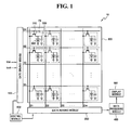
- FIG. 1 is a block diagram of an X-ray detector 10 according to an exemplary embodiment of the present invention
- FIG. 2 is a schematic diagram of a detection module 300 shown in FIG. 1
- FIG. 3 is a timing diagram for explaining the operation of the X-ray detector 10
- FIG. 4 is a circuit diagram of a data reading module 200 shown in FIG. 1
- FIG. 5 is a diagram for explaining the operation of the data reading module 200
- FIGS. 6a and 6b are diagrams for explaining variations in the charge level of a plurality of photoelectric transducers 320 shown in FIG.
- FIGS. 7a and 7b are diagrams for explaining variations in the charge level of the photoelectric transducers 320 during the generation of a dummy dark level by the detection module 300
- FIG. 8 is a diagram for explaining the operation of a data processing module 400 shown in FIG. 1 .
- the X-ray detector 10 may include the detection module 300, a gate driving module 100, the data reading module 200, the data processing module 400, a display module 500, and a control module 600.
- the detection module 300 may include a plurality of display signal lines (G1 through Gn and D1 through Dm) and a plurality of pixels PX connected to the display signal lines (G1 through Gn and D 1 through Dm) and arranged in a matrix.
- Each of the pixels may include a photoelectric transducer 320 sensing radiation and generating an amount of charge corresponding to the amount of radiation sensed, a capacitor 330 accumulating the charge generated by the photoelectric transducer 320, and a switching device 310 transmitting the charge accumulated in the capacitor 330 in response to a control signal, for example, a gate signal.
- a first end of the photoelectric transducer 320 and a first end of the capacitor 330 may be connected to, for example, the source terminal of the transistor 310, a second end of the photoelectric transducer 320 may be connected to a bias power source (not shown) or a ground source, and a second end of the capacitor 330 may be connected to a ground source.
- the detection module 300 may include a substrate 1, a plurality of the switching devices 310, a plurality of the capacitors 330, a plurality of pixel electrodes 12, a plurality of the photoelectric transducers 320, a passivation layer 20, an electrode 24, and a high-voltage direct-current (DC) power source 26.
- the photoelectric transducers 320 may generate an electric signal, that is, an electron-hole pair 6 corresponding to the intensity of an external signal, such as electric waves or magnetic waves incident thereupon.
- the photoelectric transducers 320 may serve as converters converting external radiation , for example, X-rays, into an electric signal.
- the electron-hole pair 6 may gather in each of the pixel electrodes 12, which are disposed below the photoelectric transducers 320, as charge due to a predetermined voltage Ev.
- the charge gathered in each of the pixel electrodes 12 may accumulate in a corresponding capacitor 330, which is formed along with a common electrode. Then, the charge accumulated in each of the capacitors 330 may be transmitted to the data processing module 400 and, thus, an image may be displayed.
- the display signal lines may include the gate lines G1 through Gn transmitting a gate signal and a plurality of data lines D1 through Dm transmitting an electric signal generated by each of the pixels PX to the data reading module 200.
- the gate lines G1 through Gn may extend substantially in a row direction and in parallel with one another.
- the data lines D1 through Dm may extend substantially in a column direction and are substantially parallel with one another.
- the gate driving module 300 may be provided with a gate control signal from by the control module 600 and may sequentially apply a gate signal to the gate lines G1 through Gn.
- the gate control signal is a signal for controlling the operation of the gate driving module 300, and may be obtained by combining a gate-on voltage Von and a gate-off voltage Voff provided by a gate-on/off voltage generation module (not shown).
- the data reading module 200 may be provided with a reading control signal from the control module 600 and may read an electric signal provided by the detection module 300. More specifically, the data reading module 200 may read an electric signal provided by each of the photoelectric transducers 320 and may generate a dummy dark level DDL, an offset dark level ODL, and a bright level BL. This will be described hereinbelow in more detail.
- the data processing module 400 which is provided with the dummy dark level DDL, the offset dark level ODL and the bright level BL, can ignore the dummy dark level DDL and can generate image data based on the bright level BL and the offset dark level ODL. Thereafter, the data processing module 400 transmits the image data to the display module 500 so that the display module 500 can display an image corresponding to the image data.
- the control module 600 can provide the gate control signal to the gate driving module 100 and thus control a plurality of gate signals Gout1 through Gout(n) provided to the gate lines G1 through Gn by the gate driving module 100.
- the control module 600 can provide the reading control signal to the data reading module 200 and thus control the time of generation of the dummy dark level DDL. That is, the control module 600 can control the reading of electric signals from the photoelectric transducers 320 by the data reading module 200.
- the operation of the X-ray detector 10 will hereinafter be described with reference to FIG. 3 .
- the photoelectric transducers 320 receive the radiation transmitted through the specimen and accumulate an amount of charge corresponding to the amount of radiation received in their respective capacitors 330. Thereafter, in order to read the charge accumulated in the capacitors 330, the control module 600 provides the gate control signal to the gate driving module 100. Then, the gate driving module 100 sequentially applies the gate signals Gout1 through Gout(n) to the gate lines G1 through Gn. If the switching devices 310 are turned on in response to the gate signals Gout1 through Gout(n), the charge accumulated in each of the capacitors 330 can be output to the data lines D1 through Dm.
- the data reading module 200 receives the charge levels of a plurality of rows of pixels PX respectively connected to the gate lines G1 through Gn as first through n-th line detection data in response to the application of the gate signals Gout1 through Gout(n) to the gate lines G1 through Gn. For example, if the first gate signal Gout1 is applied to the first gate line G1 during a time period between t1a and t1b, as shown in FIG. 3 , a row of pixels PX connected to the first gate line G1 are driven, and the charge accumulated in each of the capacitors 330 of the row of pixels PX connected to the first gate line G1 is transmitted to the data reading module 200 as the first line detection data through the data lines D1 through Dm.
- the data reading module 200 may include a plurality of charge-to-voltage converters 210_1 through 210_m converting the first through n-th line detection data into voltages received through the data lines D1 through Dm, a multiplexer 220 performing parallel-to-serial conversion on each of the first through n-th line detection data and an analog-to-digital converter 230 converting an analog signal provided by the multiplexer 220 into a digital signal and transmitting the digital signal to the data processing module 400.
- the structure of the data reading module 200 is not restricted to that shown in FIG. 4 . That is, the data reading module 200 may include various circuits, other than those shown in FIG. 4 (particularly, the charge-to-voltage converters 210_1 through 210_m), as long as it can convert charge received from each of the data lines D1 through Dm into a voltage.
- the data reading module 200 may have a standby period STANDBY and an irradiation period PROJECTION. More specifically, during the standby period STANDBY, the data reading module 200 may sequentially scan the gate lines G1 through Gn and may then generate a dummy dark level DDL by reading electric signals from the photoelectric transducers 320. During part of the irradiation period PROJECTION before the irradiation of a specimen, the data reading module 200 may generate an offset dark level ODL by reading electric signals from the photoelectric transducers 320.
- the data reading module 200 can generate a bright level BL by reading electric signals from the photoelectric transducers 320 during the remainder of the irradiation period PROJECTION.
- the data reading module 200 can generate the offset dark level ODL after the generation of the dummy dark level DDL.
- the gate driving module 100 sequentially applies the gate signals Gout1 through Gout(n) to the gate lines G1 through Gn, and repeatedly performs a gate scan operation GS that does not involve reading electric signals from the photoelectric transducers 320. Thereafter, the data reading module 200 can generate the dummy dark level DDL by reading electric signals from the photoelectric transducers 320. Variations in the charge level of the photoelectric transducers 320 during the repeated performing of a gate scan operation GS by the data reading module 200 are as shown in FIGS. 6a and 6b .
- the photoelectric transducers 320 may have a charge level A 1 during a period before performing the gate scan operation GS by the data reading module 200.
- the photoelectric transducers 320 may have a charge level A2 during a period after performing the gate scan operation GS by the data reading module 200.
- the charge level of the photoelectric transducers 320 may increase from A2 to A1 due to a leakage current.
- the data reading module 200 can repeatedly perform the gate scan operation GS and thus remove the charge accumulated in each of the photoelectric transducers 320 due to a leakage current. Therefore, the charge level of the photoelectric transducers 320 can be balanced, that is, can be made to vary between A 1 and A2.
- the data reading module 200 can read the electric signals from the photoelectric transducers 320 and thus generate a dummy dark level DDL during the remainder of the standby period STANDBY.
- the charge level of the photoelectric transducers 320 may be B 1 when the data reading module 200 has not yet read the electric signals from the photoelectric transducers 320, as shown in FIGS. 7a and 7b .
- the charge level B1 may be substantially the same as an increased charge level of the photoelectric transducers 320 due to a leakage current generated after a k-th gate scan operation GSk, that is, the charge level A1 of FIG. 6a .
- the data reading module 200 After the k-th gate scan operation GSk, the data reading module 200 reads the electric signals from the photoelectric transducers 320 and thus generates the dummy dark level DDL. Then, the charge level of the photoelectric transducers 320 will become level B2 shown in FIG. 7b .
- the data reading module 200 can generate more than one dummy dark level DDL by reading the electric signals from the photoelectric transducers 320 more than one time.
- the data reading module 200 can read electric signals from the photoelectric transducers 320 and thus generate an offset dark level ODL until a specimen is irradiated. Thereafter, once the irradiating of the specimen is complete, the data reading module 200 can read the electric signals from the photoelectric transducers 320 and thus generate a bright level BL (see FIG. 5 ) during the remainder of the irradiation period PROJECTION. More specifically, the data reading module 200 generates a dummy dark level DDL, and then generates an offset dark level ODL by reading electric signals from the photoelectric transducers 320. Thereafter, the data reading module 200 generates a bright level BL.
- the specimen may be irradiated more than one time.
- the charge level of the photoelectric transducers 320 during a period after the generation of the dummy dark level DDL by the data reading module 200 may be B2, which is different from the charge level of the photoelectric transducers 320 immediately after a gate scan operation, that is, the charge level A2 of FIG. 6b .
- the charge level of the photoelectric transducers 320 during a period after the generation of the offset dark level ODL by the data reading module 200 may be B2, rather than A2. That is, the charge level of the photoelectric transducers 320 may not be able to be balanced any longer after the generation of a dummy dark level DDL.
- Once an offset dark level ODL is stabilized image data can be generated based on the offset dark level ODL and a bright level BL may be stabilized. Therefore, it is possible to improve the reliability of the X-ray detector 10.
- FIG. 8 represents the flow of data from the data processing module 400.
- the data processing module 400 of FIG. 1 can receive a dummy dark level DDL, an offset dark level ODL and a bright level BL and may generate image data IMAGE DATA based only on the offset dark level ODL and the bright level BL.
- the data reading module 200 does not read any electric signals from the photoelectric transducers 320.
- the data processing module 400 can sequentially receive the dummy dark level DDL, the offset dark level ODL and the bright level BL after the k-th gate scan operation GSk.
- the data processing module 400 stores the offset dark level ODL in a memory, and can generate the image data IMAGE DATA by subtracting the offset dark level ODL from the bright level BL provided by the data reading module 200.
- FIGS. 1 through 8 it is possible to apply a stable dark level to a bright level by generating a dummy dark level and an offset dark level and applying only the offset dark level to the bright level. Therefore, it is possible to acquire precise image data and thus to improve the reliability of an X-ray detector.
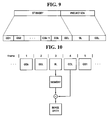
- FIG. 9 is a diagram for explaining the operation of a data reading module 200 of an X-ray detector shown in FIG. 1 according to an exemplary embodiment of the present invention
- FIG. 10 is a diagram for explaining the operation of a data processing module 400 of the X-ray detector according to the exemplary embodiment of FIG. 9 .
- the exemplary embodiment of FIG. 9 is different from the exemplary embodiment of FIGS. 1 through 8 in that the data reading module 200 generates a bright level BL first and then generates an offset dark level ODL.
- the exemplary embodiment of FIG. 9 will hereinafter be described, focusing mainly on differences with the exemplary embodiment of FIGS. 1 through 8 .
- the data reading module 200 may have a standby period STANDBY and an X-ray radiation period PROJECTION. More specifically, during the standby period STANDBY, the data reading module 200 can sequentially scan a plurality of gate lines G1 through Gn and then generate a dummy dark level DDL by reading the electric signals of a plurality of photoelectric transducers 320. During the X-ray radiation period PROJECTION, the irradiating of a specimen can be performed, and the data reading module 200 can generate a bright level BL by reading electric signals from the photoelectric transducers 320. In addition, once the specimen is X-rayed, the data reading module 200 can generate the offset dark level ODL by reading electric signals from the photoelectric transducers 320 during the remainder of the X-ray radiation period PROJECTION.
- the charge level of the photoelectric transducers 320 may be relatively balanced during the standby period STANDBY and, particularly, during a gate scan operation GS.
- the photoelectric transducers 320 has a charge level A after the repeated scanning of the gate lines G1 through Gn and has a charge level B after the generation of a dummy dark level DDL, the charge levels A and B may be different from each other.
- a specimen may be irradiated, and the data reading module 200 can generate a bright level BL and then generate an offset dark level ODL by reading the electric signals from the photoelectric transducers 320 again.
- the data processing module 400 receives a dummy dark level DDL, a bright level BL, and an offset dark level ODL from the data reading module 200, and can generate image data IMAGE DATA based only on the bright level BL and the offset dark level ODL.
- the data processing module 400 can sequentially receive the dummy dark level DDL, the bright level BL, and the offset dark level ODL after a k-th gate scan operation GSk.
- the data processing module 400 can ignore the dummy dark level DDL, and store the bright level in a memory. Then, the data processing module 400 generates the image data IMAGE DATA by subtracting the offset dark level ODL from the bright level BL.
Landscapes
- Engineering & Computer Science (AREA)
- Multimedia (AREA)
- Signal Processing (AREA)
- Health & Medical Sciences (AREA)
- Life Sciences & Earth Sciences (AREA)
- General Health & Medical Sciences (AREA)
- Physics & Mathematics (AREA)
- Medical Informatics (AREA)
- Pathology (AREA)
- Biophysics (AREA)
- Biomedical Technology (AREA)
- Immunology (AREA)
- Biochemistry (AREA)
- Computer Vision & Pattern Recognition (AREA)
- Analytical Chemistry (AREA)
- High Energy & Nuclear Physics (AREA)
- Chemical & Material Sciences (AREA)
- Nuclear Medicine, Radiotherapy & Molecular Imaging (AREA)
- Optics & Photonics (AREA)
- Radiology & Medical Imaging (AREA)
- General Physics & Mathematics (AREA)
- Heart & Thoracic Surgery (AREA)
- Molecular Biology (AREA)
- Surgery (AREA)
- Animal Behavior & Ethology (AREA)
- Public Health (AREA)
- Veterinary Medicine (AREA)
- Measurement Of Radiation (AREA)
- Apparatus For Radiation Diagnosis (AREA)
- Transforming Light Signals Into Electric Signals (AREA)
Abstract
Description
- This application claims priority from Korean Patent Application No.
10-2008-0133628 filed on December 24, 2008 - The present disclosure relates to an X-ray detector and a method of driving the same.
- Conventionally, X-ray detectors, which are a type of diagnostic radiation detector, require the photographing of specimens using X-ray sensitive films and the developing of the X-ray sensitive films in order to provide X-ray detection results for analysis.
- With recent developments in semiconductor technology, research has been conducted on digital X-ray detectors using thin-film transistors (TFTs). Digital X-ray detectors use TFTs as switching devices and can thus readily provide X-ray detection results without the need to expose and develop films.
- Initial image data obtained using TFTs, however, include not only signal components corresponding to the amount of radiation received but also offset components generated by, for example, leakage currents. Therefore, it is necessary to develop a technique for acquiring precise image data by acquiring stable offset components and correcting initial image data by removing adverse effects caused by the offset components.
- Exemplary embodiments of the present invention provide an X-ray detector having improved reliability.
- Exemplary embodiments of the present invention also provide a method of driving an X-ray detector having improved reliability.
- The above and other objects of the present invention will be described in or be understood from the following description of exemplary embodiments.
- According to an exemplary embodiment of the present invention, there is provided an X-ray detector comprising a detection module that includes a plurality of gate lines and a plurality of photoelectric transducers connected to the gate lines, respectively, and that converts X-ray radiation into an electric signal; a data reading module that sequentially scans the gate lines, generates a dummy dark level by reading electric signals of the photoelectric transducers during a standby period, generates an offset dark level by reading electric signals from the photoelectric transducers before the photographing or irradiation of a specimen, and generates a bright level by reading electric signals from the photoelectric signals after the photographing of a specimen during an X-ray projection period; and a data processing module that ignores the dummy dark level and generates image data using the bright level and the offset dark level.
- According to an exemplary embodiment of the present invention, there is provided an X-ray detector comprising a detection module that includes a plurality of gate lines and a plurality of photoelectric transducers connected to the gate lines, respectively, and that converts X-ray radiation into an electric signal; a data reading module that sequentially scans the gate lines, generates a dummy dark level by reading electric signals of the photoelectric transducers during a standby period, generates a bright level by reading electric signals from the photoelectric transducers after the photographing or irradiation of a specimen, and then generates an offset dark level by reading electric signals from the photoelectric signals during an X-ray projection period; and a data processing module that ignores the dummy dark level and generates image data using the bright level and the offset dark level.
- According to an exemplary embodiment of the present invention, there is provided a method of driving an X-ray detector comprising providing a plurality of gate lines and a plurality of photoelectric transducers connected to the gate lines, respectively, and converting X-ray radiation into an electric signal; sequentially scanning the gate lines and generating a dummy dark level by reading electric signals of the photoelectric transducers during a standby period; generating an offset dark level before the photographing or irradiation of a specimen by reading electric signals from the photoelectric transducers and generating a bright level by reading electric signals from the photoelectric signals during an X-ray projection period; and ignoring the dummy dark level and generating image data using the bright level and the offset dark level.
- According to an exemplary embodiment of the present invention, there is provided a method of driving an X-ray detector comprising providing a plurality of gate lines and a plurality of photoelectric transducers connected to the gate lines, respectively, and converting X-ray radiation into an electric signal; sequentially scanning the gate lines and generating a dummy dark level by reading electric signals of the photoelectric transducers during a standby period; generating a bright level after the photographing or irradiation of a specimen by reading electric signals from the photoelectric transducers and generating an offset dark level by reading electric signals from the photoelectric signals during an X-ray projection period; and ignoring the dummy dark level and generating image data using the bright level and the offset dark level.
-
-
FIG. 1 is a block diagram of an X-ray detector according to an exemplary embodiment of the present invention; -
FIG. 2 is a schematic diagram of a detection module used in the detector shown inFIG. 1 ; -
FIG. 3 is a timing diagram for explaining the operation of the X-ray detector shown inFIG. 1 ; -
FIG. 4 is a circuit diagram of a data reading module used in the detector shown inFIG. 1 ; -
FIG. 5 is a diagram for explaining the operation of the data reading module used in the detector shown inFIG. 1 ; -
FIGS. 6a and 6b are diagrams for explaining variations in the charge level of a plurality of photoelectric transducers shown inFIG. 1 during the scanning of a plurality of gate lines by the detection module used in the detector shown inFIG. 1 ; -
FIGS. 7a and 7b are diagrams for explaining variations in the charge level of the photoelectric transducers used in the detector shown inFIG. 1 during the generation of a dummy dark level by the detection module used in the detector shown inFIG. 1 ; -
FIG. 8 is a diagram for explaining the operation of a data processing module used in the detector shown inFIG. 1 ; -
FIG. 9 is a diagram for explaining the operation of a data reading module of an X-ray detector according to an exemplary embodiment of the present invention; and -
FIG. 10 is a diagram for explaining the operation of a data processing module of the X-ray detector according to the exemplary embodiment ofFIG. 9 . - Advantages and features of the present invention and methods of accomplishing the same may be understood more readily by reference to the following detailed description of exemplary embodiments and the accompanying drawings. The present invention may, however, be embodied in many different forms and should not be construed as being limited to the exemplary embodiments set forth herein. Rather, these exemplary embodiments are provided so that this disclosure will be thorough and complete and will fully convey the concept of the invention to those of ordinary skill in the art, and the present invention will only be defined by the appended claims. Like reference numerals refer to like elements throughout the specification.
- Hereinafter, an X-ray detector and a method of driving the same, according to exemplary embodiments of the present invention, will be described in detail with reference to
FIGS. 1 through 8 .FIG. 1 is a block diagram of anX-ray detector 10 according to an exemplary embodiment of the present invention,FIG. 2 is a schematic diagram of adetection module 300 shown inFIG. 1 ,FIG. 3 is a timing diagram for explaining the operation of theX-ray detector 10,FIG. 4 is a circuit diagram of adata reading module 200 shown inFIG. 1 ,FIG. 5 is a diagram for explaining the operation of thedata reading module 200,FIGS. 6a and 6b are diagrams for explaining variations in the charge level of a plurality ofphotoelectric transducers 320 shown inFIG. 1 during the scanning of a plurality of gate lines G1 through Gn by thedetection module 300,FIGS. 7a and 7b are diagrams for explaining variations in the charge level of thephotoelectric transducers 320 during the generation of a dummy dark level by thedetection module 300,FIG. 8 is a diagram for explaining the operation of adata processing module 400 shown inFIG. 1 . - Referring to
FIG. 1 , theX-ray detector 10 may include thedetection module 300, agate driving module 100, thedata reading module 200, thedata processing module 400, adisplay module 500, and acontrol module 600. - The
detection module 300 may include a plurality of display signal lines (G1 through Gn and D1 through Dm) and a plurality of pixels PX connected to the display signal lines (G1 through Gn andD 1 through Dm) and arranged in a matrix. Each of the pixels may include aphotoelectric transducer 320 sensing radiation and generating an amount of charge corresponding to the amount of radiation sensed, acapacitor 330 accumulating the charge generated by thephotoelectric transducer 320, and aswitching device 310 transmitting the charge accumulated in thecapacitor 330 in response to a control signal, for example, a gate signal. More specifically, a first end of thephotoelectric transducer 320 and a first end of thecapacitor 330 may be connected to, for example, the source terminal of thetransistor 310, a second end of thephotoelectric transducer 320 may be connected to a bias power source (not shown) or a ground source, and a second end of thecapacitor 330 may be connected to a ground source. - Referring to
FIG. 2 , thedetection module 300 may include asubstrate 1, a plurality of theswitching devices 310, a plurality of thecapacitors 330, a plurality ofpixel electrodes 12, a plurality of thephotoelectric transducers 320, a passivation layer 20, anelectrode 24, and a high-voltage direct-current (DC)power source 26. Thephotoelectric transducers 320 may generate an electric signal, that is, an electron-hole pair 6 corresponding to the intensity of an external signal, such as electric waves or magnetic waves incident thereupon. Thephotoelectric transducers 320 may serve as converters converting external radiation , for example, X-rays, into an electric signal. The electron-hole pair 6 may gather in each of thepixel electrodes 12, which are disposed below thephotoelectric transducers 320, as charge due to a predetermined voltage Ev. The charge gathered in each of thepixel electrodes 12 may accumulate in acorresponding capacitor 330, which is formed along with a common electrode. Then, the charge accumulated in each of thecapacitors 330 may be transmitted to thedata processing module 400 and, thus, an image may be displayed. - Referring to
FIG. 1 , the display signal lines (G1 through Gn and D1 through Dm) may include the gate lines G1 through Gn transmitting a gate signal and a plurality of data lines D1 through Dm transmitting an electric signal generated by each of the pixels PX to thedata reading module 200. The gate lines G1 through Gn may extend substantially in a row direction and in parallel with one another. The data lines D1 through Dm may extend substantially in a column direction and are substantially parallel with one another. - The
gate driving module 300 may be provided with a gate control signal from by thecontrol module 600 and may sequentially apply a gate signal to the gate lines G1 through Gn. The gate control signal is a signal for controlling the operation of thegate driving module 300, and may be obtained by combining a gate-on voltage Von and a gate-off voltage Voff provided by a gate-on/off voltage generation module (not shown). - The
data reading module 200 may be provided with a reading control signal from thecontrol module 600 and may read an electric signal provided by thedetection module 300. More specifically, thedata reading module 200 may read an electric signal provided by each of thephotoelectric transducers 320 and may generate a dummy dark level DDL, an offset dark level ODL, and a bright level BL. This will be described hereinbelow in more detail. - The
data processing module 400 which is provided with the dummy dark level DDL, the offset dark level ODL and the bright level BL, can ignore the dummy dark level DDL and can generate image data based on the bright level BL and the offset dark level ODL. Thereafter, thedata processing module 400 transmits the image data to thedisplay module 500 so that thedisplay module 500 can display an image corresponding to the image data. - The
control module 600 can provide the gate control signal to thegate driving module 100 and thus control a plurality of gate signals Gout1 through Gout(n) provided to the gate lines G1 through Gn by thegate driving module 100. In addition, thecontrol module 600 can provide the reading control signal to thedata reading module 200 and thus control the time of generation of the dummy dark level DDL. That is, thecontrol module 600 can control the reading of electric signals from thephotoelectric transducers 320 by thedata reading module 200. - The operation of the
X-ray detector 10 will hereinafter be described with reference toFIG. 3 . - Referring to
FIG. 3 , if a specimen (not shown) is irradiated by X-rays during a time period between Ta and Tb, thephotoelectric transducers 320 receive the radiation transmitted through the specimen and accumulate an amount of charge corresponding to the amount of radiation received in theirrespective capacitors 330. Thereafter, in order to read the charge accumulated in thecapacitors 330, thecontrol module 600 provides the gate control signal to thegate driving module 100. Then, thegate driving module 100 sequentially applies the gate signals Gout1 through Gout(n) to the gate lines G1 through Gn. If theswitching devices 310 are turned on in response to the gate signals Gout1 through Gout(n), the charge accumulated in each of thecapacitors 330 can be output to the data lines D1 through Dm. - The
data reading module 200 receives the charge levels of a plurality of rows of pixels PX respectively connected to the gate lines G1 through Gn as first through n-th line detection data in response to the application of the gate signals Gout1 through Gout(n) to the gate lines G1 through Gn. For example, if the first gate signal Gout1 is applied to the first gate line G1 during a time period between t1a and t1b, as shown inFIG. 3 , a row of pixels PX connected to the first gate line G1 are driven, and the charge accumulated in each of thecapacitors 330 of the row of pixels PX connected to the first gate line G1 is transmitted to thedata reading module 200 as the first line detection data through the data lines D1 through Dm. - The structure and operation of the
data reading module 200 will hereinafter be described in detail with reference toFIGS. 4 through 7b . - Referring to
FIG. 4 , thedata reading module 200 may include a plurality of charge-to-voltage converters 210_1 through 210_m converting the first through n-th line detection data into voltages received through the data lines D1 through Dm, amultiplexer 220 performing parallel-to-serial conversion on each of the first through n-th line detection data and an analog-to-digital converter 230 converting an analog signal provided by themultiplexer 220 into a digital signal and transmitting the digital signal to thedata processing module 400. The structure of thedata reading module 200 is not restricted to that shown inFIG. 4 . That is, thedata reading module 200 may include various circuits, other than those shown inFIG. 4 (particularly, the charge-to-voltage converters 210_1 through 210_m), as long as it can convert charge received from each of the data lines D1 through Dm into a voltage. - Referring to
FIG. 5 , thedata reading module 200 may have a standby period STANDBY and an irradiation period PROJECTION. More specifically, during the standby period STANDBY, thedata reading module 200 may sequentially scan the gate lines G1 through Gn and may then generate a dummy dark level DDL by reading electric signals from thephotoelectric transducers 320. During part of the irradiation period PROJECTION before the irradiation of a specimen, thedata reading module 200 may generate an offset dark level ODL by reading electric signals from thephotoelectric transducers 320. Once the specimen is irradiated with the X-rays, thedata reading module 200 can generate a bright level BL by reading electric signals from thephotoelectric transducers 320 during the remainder of the irradiation period PROJECTION. Thedata reading module 200 can generate the offset dark level ODL after the generation of the dummy dark level DDL. - During the standby period STANDBY, the
gate driving module 100 sequentially applies the gate signals Gout1 through Gout(n) to the gate lines G1 through Gn, and repeatedly performs a gate scan operation GS that does not involve reading electric signals from thephotoelectric transducers 320. Thereafter, thedata reading module 200 can generate the dummy dark level DDL by reading electric signals from thephotoelectric transducers 320. Variations in the charge level of thephotoelectric transducers 320 during the repeated performing of a gate scan operation GS by thedata reading module 200 are as shown inFIGS. 6a and 6b . - Referring to
FIGS. 6a and 6b , thephotoelectric transducers 320 may have acharge level A 1 during a period before performing the gate scan operation GS by thedata reading module 200. On the other hand, thephotoelectric transducers 320 may have a charge level A2 during a period after performing the gate scan operation GS by thedata reading module 200. During a time period between the end of the gate scan operation GS and the beginning of another gate scan operation GS, however, the charge level of thephotoelectric transducers 320 may increase from A2 to A1 due to a leakage current. In order to address this problem, thedata reading module 200 can repeatedly perform the gate scan operation GS and thus remove the charge accumulated in each of thephotoelectric transducers 320 due to a leakage current. Therefore, the charge level of thephotoelectric transducers 320 can be balanced, that is, can be made to vary betweenA 1 and A2. - Once the repeated scanning of the gate lines G1 through Gn is complete, the
data reading module 200 can read the electric signals from thephotoelectric transducers 320 and thus generate a dummy dark level DDL during the remainder of the standby period STANDBY. The charge level of thephotoelectric transducers 320 may beB 1 when thedata reading module 200 has not yet read the electric signals from thephotoelectric transducers 320, as shown inFIGS. 7a and 7b . The charge level B1 may be substantially the same as an increased charge level of thephotoelectric transducers 320 due to a leakage current generated after a k-th gate scan operation GSk, that is, the charge level A1 ofFIG. 6a . - After the k-th gate scan operation GSk, the
data reading module 200 reads the electric signals from thephotoelectric transducers 320 and thus generates the dummy dark level DDL. Then, the charge level of thephotoelectric transducers 320 will become level B2 shown inFIG. 7b . Thedata reading module 200 can generate more than one dummy dark level DDL by reading the electric signals from thephotoelectric transducers 320 more than one time. - During the X-ray irradiation period PROJECTION, the
data reading module 200 can read electric signals from thephotoelectric transducers 320 and thus generate an offset dark level ODL until a specimen is irradiated. Thereafter, once the irradiating of the specimen is complete, thedata reading module 200 can read the electric signals from thephotoelectric transducers 320 and thus generate a bright level BL (seeFIG. 5 ) during the remainder of the irradiation period PROJECTION. More specifically, thedata reading module 200 generates a dummy dark level DDL, and then generates an offset dark level ODL by reading electric signals from thephotoelectric transducers 320. Thereafter, thedata reading module 200 generates a bright level BL. During the irradiation period PROJECTION, the specimen may be irradiated more than one time. - The charge level of the
photoelectric transducers 320 during a period after the generation of the dummy dark level DDL by thedata reading module 200 may be B2, which is different from the charge level of thephotoelectric transducers 320 immediately after a gate scan operation, that is, the charge level A2 ofFIG. 6b . Thus, the charge level of thephotoelectric transducers 320 during a period after the generation of the offset dark level ODL by thedata reading module 200 may be B2, rather than A2. That is, the charge level of thephotoelectric transducers 320 may not be able to be balanced any longer after the generation of a dummy dark level DDL. Thus, it is possible to generate a stable offset dark level ODL by reading electric signals from thephotoelectric transducers 320 again. Once an offset dark level ODL is stabilized, image data can be generated based on the offset dark level ODL and a bright level BL may be stabilized. Therefore, it is possible to improve the reliability of theX-ray detector 10. - The operation of the
data processing module 400 will hereinafter be described in detail with reference toFIG. 8 , which represents the flow of data from thedata processing module 400. - Referring to
FIG. 8 , thedata processing module 400 ofFIG. 1 can receive a dummy dark level DDL, an offset dark level ODL and a bright level BL and may generate image data IMAGE DATA based only on the offset dark level ODL and the bright level BL. During a gate scan operation GS performed by thegate driving module 100, thedata reading module 200 does not read any electric signals from thephotoelectric transducers 320. Thus, thedata processing module 400 can sequentially receive the dummy dark level DDL, the offset dark level ODL and the bright level BL after the k-th gate scan operation GSk. Thedata processing module 400 stores the offset dark level ODL in a memory, and can generate the image data IMAGE DATA by subtracting the offset dark level ODL from the bright level BL provided by thedata reading module 200. - According to the exemplary embodiment of
FIGS. 1 through 8 , it is possible to apply a stable dark level to a bright level by generating a dummy dark level and an offset dark level and applying only the offset dark level to the bright level. Therefore, it is possible to acquire precise image data and thus to improve the reliability of an X-ray detector. - An X-ray detector and a method of driving the same, according to an exemplary embodiment of the present invention, will hereinafter be described in detail with reference to
FIGS. 9 and 10. FIG. 9 is a diagram for explaining the operation of adata reading module 200 of an X-ray detector shown inFIG. 1 according to an exemplary embodiment of the present invention, andFIG. 10 is a diagram for explaining the operation of adata processing module 400 of the X-ray detector according to the exemplary embodiment ofFIG. 9 . - The exemplary embodiment of
FIG. 9 is different from the exemplary embodiment ofFIGS. 1 through 8 in that thedata reading module 200 generates a bright level BL first and then generates an offset dark level ODL. For convenience, the exemplary embodiment ofFIG. 9 will hereinafter be described, focusing mainly on differences with the exemplary embodiment ofFIGS. 1 through 8 . - Referring to
FIG. 9 , thedata reading module 200 may have a standby period STANDBY and an X-ray radiation period PROJECTION. More specifically, during the standby period STANDBY, thedata reading module 200 can sequentially scan a plurality of gate lines G1 through Gn and then generate a dummy dark level DDL by reading the electric signals of a plurality ofphotoelectric transducers 320. During the X-ray radiation period PROJECTION, the irradiating of a specimen can be performed, and thedata reading module 200 can generate a bright level BL by reading electric signals from thephotoelectric transducers 320. In addition, once the specimen is X-rayed, thedata reading module 200 can generate the offset dark level ODL by reading electric signals from thephotoelectric transducers 320 during the remainder of the X-ray radiation period PROJECTION. - In the exemplary embodiment of
FIGS. 9 and 10 , like in the exemplary embodiment ofFIGS. 1 through 8 , the charge level of thephotoelectric transducers 320 may be relatively balanced during the standby period STANDBY and, particularly, during a gate scan operation GS. Thus, thephotoelectric transducers 320 has a charge level A after the repeated scanning of the gate lines G1 through Gn and has a charge level B after the generation of a dummy dark level DDL, the charge levels A and B may be different from each other. During the X-ray radiation period PROJECTION, a specimen may be irradiated, and thedata reading module 200 can generate a bright level BL and then generate an offset dark level ODL by reading the electric signals from thephotoelectric transducers 320 again. - Referring to
FIG. 10 , thedata processing module 400 receives a dummy dark level DDL, a bright level BL, and an offset dark level ODL from thedata reading module 200, and can generate image data IMAGE DATA based only on the bright level BL and the offset dark level ODL. - More specifically, the
data processing module 400 can sequentially receive the dummy dark level DDL, the bright level BL, and the offset dark level ODL after a k-th gate scan operation GSk. Thedata processing module 400 can ignore the dummy dark level DDL, and store the bright level in a memory. Then, thedata processing module 400 generates the image data IMAGE DATA by subtracting the offset dark level ODL from the bright level BL. - According to the exemplary embodiment of
FIGS. 9 and 10 , it is possible to apply a stable dark level to a bright level by generating a dummy dark level and an offset dark level and applying only the offset dark level to the bright level. Therefore, it is possible to acquire precise image data and thus to improve the reliability of an X-ray detector.
Claims (15)
- An X-ray detector comprising:a detection module that includes a plurality of gate lines and a plurality of photoelectric transducers connected to the gate lines, respectively, to convert X-ray radiation into electric signals;a data reading module that sequentially scans the plurality of gate lines, generates a dummy dark level by reading the electric signals of the plurality of photoelectric transducers during a standby period, generates an offset dark level by reading the electric signals from the plurality of photoelectric transducers before irradiating a specimen, and generates a bright level by reading the electric signals from the photoelectric transducers after the irradiation of a specimen, during an X-ray radiation period; anda data processing module generates image data using the bright level and the offset dark level.
- The X-ray detector of claim 1, wherein the data reading module generates the offset dark level immediately after the generation of the dummy dark level.
- The X-ray detector of claim 2, wherein the data reading module generates more than one dummy dark level by reading the electric signals from the photoelectric transducers more than one time.
- The X-ray detector of claim 1, further comprising a control module that provides a control signal to the data reading module to control the generation of the dummy dark level.
- The X-ray detector of claim 1, wherein the data processing module stores the offset dark level and generates the image data by subtracting the offset dark level from the bright level.
- The X-ray detector of claim 1, wherein the X-ray detector irradiates the specimen more than one time during the X-ray radiation period.
- An X-ray detector comprising:a detection module that includes a plurality of gate lines and a plurality of photoelectric transducers connected to the plurality of gate lines, respectively, to convert X-ray radiation into electric signals;a data reading module that sequentially scans the plurality of gate lines generates a dummy dark level by reading the electric signals of the plurality of photoelectric transducers during a standby period, generates a bright level by reading the electric signals from the plurality of photoelectric transducers after irradiating a specimen, and then generates an offset dark level by reading the electric signals from the plurality of photoelectric transducers during an irradiation period; anda data processing module generates image data using the bright level and the offset dark level.
- The X-ray detector of claim 7, wherein the data reading module generates the bright level immediately after generation of the dummy dark level.
- The X-ray detector of claim 8, wherein the data reading module generates more than one dummy dark level by reading the electric signals from the plurality of photoelectric transducers more than one time.
- The X-ray detector of claim 7, wherein the data processing module stores the bright level and generates the image data by subtracting the offset dark level from the bright level.
- The X-ray detector of claim 7, wherein the X-ray detector irradiates the specimen more than one time during the irradiation period.
- A method of driving an X-ray detector, the method comprising:providing a plurality of gate lines and a plurality of photoelectric transducers connected to the plurality of gate lines, respectively, and converting X-ray radiation into electric signals;sequentially scanning the gate lines and generating a dummy dark level by reading the electric signals of the plurality of photoelectric transducers during a standby period;generating an offset dark level before irradiating a specimen by reading the electric signals from the plurality of photoelectric transducers and generating a bright level by reading the electric signals from the plurality of photoelectric transducers during an X-ray radiation period; andignoring the dummy dark level and generating image data using only the bright level and the offset dark level.
- The method of claim 12, wherein the generating of the offset dark level comprises generating the offset dark level immediately after the generating of the dummy dark level.
- The method of claim 13, wherein the generating of the dummy dark level comprises generating more than one dummy dark level by reading the electric signals from the plurality of photoelectric transducers more than one time.
- The method of claim 12, wherein the generating of the image data comprises storing the offset dark level and generating the image data by subtracting the offset dark level from the bright level.
Applications Claiming Priority (1)
| Application Number | Priority Date | Filing Date | Title |
|---|---|---|---|
| KR1020080133628A KR101571044B1 (en) | 2008-12-24 | 2008-12-24 | Radiation detection apparatus and driving method thereof |
Publications (2)
| Publication Number | Publication Date |
|---|---|
| EP2202961A2 true EP2202961A2 (en) | 2010-06-30 |
| EP2202961A3 EP2202961A3 (en) | 2015-04-01 |
Family
ID=42046237
Family Applications (1)
| Application Number | Title | Priority Date | Filing Date |
|---|---|---|---|
| EP09011362.2A Withdrawn EP2202961A3 (en) | 2008-12-24 | 2009-09-04 | X-ray detector and method of driving the same |
Country Status (3)
| Country | Link |
|---|---|
| US (1) | US7915594B2 (en) |
| EP (1) | EP2202961A3 (en) |
| KR (1) | KR101571044B1 (en) |
Families Citing this family (5)
| Publication number | Priority date | Publication date | Assignee | Title |
|---|---|---|---|---|
| FR2921756B1 (en) * | 2007-09-27 | 2009-12-25 | Commissariat Energie Atomique | PIXEL MATRIX HAVING VOLTAGE REGULATORS. |
| US8791419B2 (en) * | 2010-12-15 | 2014-07-29 | Carestream Health, Inc. | High charge capacity pixel architecture, photoelectric conversion apparatus, radiation image pickup system and methods for same |
| CN106252371B (en) * | 2016-08-23 | 2019-07-16 | 上海奕瑞光电子科技股份有限公司 | A kind of radioscopic image sensor and the method for correcting image interference |
| CN106206637B (en) * | 2016-08-23 | 2019-07-16 | 上海奕瑞光电子科技股份有限公司 | An X-ray image sensor and method for correcting image interference |
| KR102860701B1 (en) * | 2023-01-11 | 2025-09-17 | 주식회사 레이언스 | X-ray detector and image processing device |
Citations (1)
| Publication number | Priority date | Publication date | Assignee | Title |
|---|---|---|---|---|
| EP1477932A2 (en) * | 2003-05-16 | 2004-11-17 | Canon Kabushiki Kaisha | Radiation imaging apparatus |
Family Cites Families (8)
| Publication number | Priority date | Publication date | Assignee | Title |
|---|---|---|---|---|
| JP3897389B2 (en) * | 1996-02-22 | 2007-03-22 | キヤノン株式会社 | Photoelectric conversion device driving method and photoelectric conversion device |
| US6448561B1 (en) * | 1996-02-26 | 2002-09-10 | Canon Kabushiki Kaisha | Photoelectric conversion apparatus and driving method of the apparatus |
| US5920070A (en) * | 1996-11-27 | 1999-07-06 | General Electric Company | Solid state area x-ray detector with adjustable bias |
| US6904126B2 (en) * | 2002-06-19 | 2005-06-07 | Canon Kabushiki Kaisha | Radiological imaging apparatus and method |
| JP2005287773A (en) * | 2004-03-31 | 2005-10-20 | Canon Inc | Image photographing apparatus and image photographing system |
| JP4744831B2 (en) | 2004-09-09 | 2011-08-10 | 株式会社東芝 | X-ray diagnostic equipment |
| JP4965931B2 (en) * | 2005-08-17 | 2012-07-04 | キヤノン株式会社 | Radiation imaging apparatus, radiation imaging system, control method thereof, and control program |
| JP2007151761A (en) | 2005-12-02 | 2007-06-21 | Canon Inc | Radiation imaging apparatus, system and method, and program |
-
2008
- 2008-12-24 KR KR1020080133628A patent/KR101571044B1/en active Active
-
2009
- 2009-08-10 US US12/538,284 patent/US7915594B2/en not_active Expired - Fee Related
- 2009-09-04 EP EP09011362.2A patent/EP2202961A3/en not_active Withdrawn
Patent Citations (1)
| Publication number | Priority date | Publication date | Assignee | Title |
|---|---|---|---|---|
| EP1477932A2 (en) * | 2003-05-16 | 2004-11-17 | Canon Kabushiki Kaisha | Radiation imaging apparatus |
Also Published As
| Publication number | Publication date |
|---|---|
| KR20100075029A (en) | 2010-07-02 |
| US20100155613A1 (en) | 2010-06-24 |
| EP2202961A3 (en) | 2015-04-01 |
| US7915594B2 (en) | 2011-03-29 |
| KR101571044B1 (en) | 2015-11-24 |
Similar Documents
| Publication | Publication Date | Title |
|---|---|---|
| JP5361628B2 (en) | Imaging apparatus and imaging system, control method thereof, and program thereof | |
| US8809795B2 (en) | Imaging apparatus, radiation imaging system, controlling method of imaging apparatus, and recording medium recording control program of imaging apparatus | |
| JP5792923B2 (en) | Radiation imaging apparatus, radiation imaging system, control method thereof, and program thereof | |
| US7227926B2 (en) | Imaging apparatus and imaging system | |
| JP5642166B2 (en) | Imaging system and control method thereof | |
| US9256306B2 (en) | Sensing apparatus and driving method thereof | |
| US8680471B2 (en) | Imaging apparatus, imaging system, method of controlling the apparatus and the system, and program | |
| US20110095169A1 (en) | Imaging apparatus, imaging system, method of controlling the apparatus and the system, and program | |
| CN110971843B (en) | Radiographic apparatus, control method thereof, and radiographic system | |
| CN102640017B (en) | Image pickup device, image pickup system, control method therefor | |
| US7915594B2 (en) | X-ray detector and method of driving the same | |
| CN102525493A (en) | Imaging apparatus, imaging system, and method for controlling imaging apparatus | |
| WO2018135293A1 (en) | Radiation imaging device and radiation imaging system | |
| US8410450B2 (en) | Apparatus for detecting X-rays and method of operating the same | |
| US20090184253A1 (en) | Light or radiation image pickup apparatus | |
| JP3696176B2 (en) | Imaging device | |
| CN106252371B (en) | A kind of radioscopic image sensor and the method for correcting image interference | |
| CN106129078A (en) | A kind of radioscopic image sensor and the method for correction image disruption thereof | |
| CN106206637B (en) | An X-ray image sensor and method for correcting image interference | |
| US10695015B2 (en) | Solid-state image capturing device, radiation image capturing system, and method of controlling solid-state image capturing device | |
| WO2020149098A1 (en) | Radiographic imaging device and radiographic imaging system | |
| JP2023063061A (en) | Radiation imaging control device, radiation imaging control method and program | |
| JP2014030216A (en) | Imaging apparatus, imaging system, control method of imaging apparatus and imaging system and program of the same |
Legal Events
| Date | Code | Title | Description |
|---|---|---|---|
| PUAI | Public reference made under article 153(3) epc to a published international application that has entered the european phase |
Free format text: ORIGINAL CODE: 0009012 |
|
| AK | Designated contracting states |
Kind code of ref document: A2 Designated state(s): AT BE BG CH CY CZ DE DK EE ES FI FR GB GR HR HU IE IS IT LI LT LU LV MC MK MT NL NO PL PT RO SE SI SK SM TR |
|
| AX | Request for extension of the european patent |
Extension state: AL BA RS |
|
| RAP1 | Party data changed (applicant data changed or rights of an application transferred) |
Owner name: SAMSUNG ELECTRONICS CO., LTD. |
|
| RAP1 | Party data changed (applicant data changed or rights of an application transferred) |
Owner name: SAMSUNG DISPLAY CO., LTD. |
|
| PUAL | Search report despatched |
Free format text: ORIGINAL CODE: 0009013 |
|
| AK | Designated contracting states |
Kind code of ref document: A3 Designated state(s): AT BE BG CH CY CZ DE DK EE ES FI FR GB GR HR HU IE IS IT LI LT LU LV MC MK MT NL NO PL PT RO SE SI SK SM TR |
|
| AX | Request for extension of the european patent |
Extension state: AL BA RS |
|
| RIC1 | Information provided on ipc code assigned before grant |
Ipc: H04N 5/217 20110101ALI20150223BHEP Ipc: H04N 5/32 20060101AFI20150223BHEP |
|
| 17P | Request for examination filed |
Effective date: 20150507 |
|
| RBV | Designated contracting states (corrected) |
Designated state(s): AT BE BG CH CY CZ DE DK EE ES FI FR GB GR HR HU IE IS IT LI LT LU LV MC MK MT NL NO PL PT RO SE SI SK SM TR |
|
| 17Q | First examination report despatched |
Effective date: 20150601 |
|
| RAP1 | Party data changed (applicant data changed or rights of an application transferred) |
Owner name: SAMSUNG DISPLAY CO., LTD. |
|
| STAA | Information on the status of an ep patent application or granted ep patent |
Free format text: STATUS: THE APPLICATION IS DEEMED TO BE WITHDRAWN |
|
| 18D | Application deemed to be withdrawn |
Effective date: 20180626 |