EP2202801A2 - Compound semiconductor device and manufacturing method of the same - Google Patents
Compound semiconductor device and manufacturing method of the same Download PDFInfo
- Publication number
- EP2202801A2 EP2202801A2 EP09171693A EP09171693A EP2202801A2 EP 2202801 A2 EP2202801 A2 EP 2202801A2 EP 09171693 A EP09171693 A EP 09171693A EP 09171693 A EP09171693 A EP 09171693A EP 2202801 A2 EP2202801 A2 EP 2202801A2
- Authority
- EP
- European Patent Office
- Prior art keywords
- layer
- electrode
- compound semiconductor
- gan layer
- semiconductor device
- Prior art date
- Legal status (The legal status is an assumption and is not a legal conclusion. Google has not performed a legal analysis and makes no representation as to the accuracy of the status listed.)
- Granted
Links
Images






Classifications
-
- H—ELECTRICITY
- H10—SEMICONDUCTOR DEVICES; ELECTRIC SOLID-STATE DEVICES NOT OTHERWISE PROVIDED FOR
- H10D—INORGANIC ELECTRIC SEMICONDUCTOR DEVICES
- H10D62/00—Semiconductor bodies, or regions thereof, of devices having potential barriers
- H10D62/10—Shapes, relative sizes or dispositions of the regions of the semiconductor bodies; Shapes of the semiconductor bodies
- H10D62/102—Constructional design considerations for preventing surface leakage or controlling electric field concentration
- H10D62/103—Constructional design considerations for preventing surface leakage or controlling electric field concentration for increasing or controlling the breakdown voltage of reverse-biased devices
- H10D62/105—Constructional design considerations for preventing surface leakage or controlling electric field concentration for increasing or controlling the breakdown voltage of reverse-biased devices by having particular doping profiles, shapes or arrangements of PN junctions; by having supplementary regions, e.g. junction termination extension [JTE]
- H10D62/106—Constructional design considerations for preventing surface leakage or controlling electric field concentration for increasing or controlling the breakdown voltage of reverse-biased devices by having particular doping profiles, shapes or arrangements of PN junctions; by having supplementary regions, e.g. junction termination extension [JTE] having supplementary regions doped oppositely to or in rectifying contact with regions of the semiconductor bodies, e.g. guard rings with PN or Schottky junctions
-
- H—ELECTRICITY
- H10—SEMICONDUCTOR DEVICES; ELECTRIC SOLID-STATE DEVICES NOT OTHERWISE PROVIDED FOR
- H10D—INORGANIC ELECTRIC SEMICONDUCTOR DEVICES
- H10D30/00—Field-effect transistors [FET]
- H10D30/01—Manufacture or treatment
- H10D30/015—Manufacture or treatment of FETs having heterojunction interface channels or heterojunction gate electrodes, e.g. HEMT
-
- H—ELECTRICITY
- H10—SEMICONDUCTOR DEVICES; ELECTRIC SOLID-STATE DEVICES NOT OTHERWISE PROVIDED FOR
- H10D—INORGANIC ELECTRIC SEMICONDUCTOR DEVICES
- H10D30/00—Field-effect transistors [FET]
- H10D30/40—FETs having zero-dimensional [0D], one-dimensional [1D] or two-dimensional [2D] charge carrier gas channels
- H10D30/47—FETs having zero-dimensional [0D], one-dimensional [1D] or two-dimensional [2D] charge carrier gas channels having two-dimensional [2D] charge carrier gas channels, e.g. nanoribbon FETs or high electron mobility transistors [HEMT]
- H10D30/471—High electron mobility transistors [HEMT] or high hole mobility transistors [HHMT]
- H10D30/475—High electron mobility transistors [HEMT] or high hole mobility transistors [HHMT] having wider bandgap layer formed on top of lower bandgap active layer, e.g. undoped barrier HEMTs such as i-AlGaN/GaN HEMTs
- H10D30/4755—High electron mobility transistors [HEMT] or high hole mobility transistors [HHMT] having wider bandgap layer formed on top of lower bandgap active layer, e.g. undoped barrier HEMTs such as i-AlGaN/GaN HEMTs having wide bandgap charge-carrier supplying layers, e.g. modulation doped HEMTs such as n-AlGaAs/GaAs HEMTs
-
- H—ELECTRICITY
- H10—SEMICONDUCTOR DEVICES; ELECTRIC SOLID-STATE DEVICES NOT OTHERWISE PROVIDED FOR
- H10D—INORGANIC ELECTRIC SEMICONDUCTOR DEVICES
- H10D30/00—Field-effect transistors [FET]
- H10D30/40—FETs having zero-dimensional [0D], one-dimensional [1D] or two-dimensional [2D] charge carrier gas channels
- H10D30/47—FETs having zero-dimensional [0D], one-dimensional [1D] or two-dimensional [2D] charge carrier gas channels having two-dimensional [2D] charge carrier gas channels, e.g. nanoribbon FETs or high electron mobility transistors [HEMT]
- H10D30/471—High electron mobility transistors [HEMT] or high hole mobility transistors [HHMT]
- H10D30/477—Vertical HEMTs or vertical HHMTs
-
- H—ELECTRICITY
- H10—SEMICONDUCTOR DEVICES; ELECTRIC SOLID-STATE DEVICES NOT OTHERWISE PROVIDED FOR
- H10D—INORGANIC ELECTRIC SEMICONDUCTOR DEVICES
- H10D30/00—Field-effect transistors [FET]
- H10D30/60—Insulated-gate field-effect transistors [IGFET]
- H10D30/611—Insulated-gate field-effect transistors [IGFET] having multiple independently-addressable gate electrodes influencing the same channel
- H10D30/615—Insulated-gate field-effect transistors [IGFET] having multiple independently-addressable gate electrodes influencing the same channel comprising a MOS gate electrode and at least one non-MOS gate electrode
-
- H—ELECTRICITY
- H10—SEMICONDUCTOR DEVICES; ELECTRIC SOLID-STATE DEVICES NOT OTHERWISE PROVIDED FOR
- H10D—INORGANIC ELECTRIC SEMICONDUCTOR DEVICES
- H10D62/00—Semiconductor bodies, or regions thereof, of devices having potential barriers
- H10D62/10—Shapes, relative sizes or dispositions of the regions of the semiconductor bodies; Shapes of the semiconductor bodies
- H10D62/117—Shapes of semiconductor bodies
-
- H—ELECTRICITY
- H10—SEMICONDUCTOR DEVICES; ELECTRIC SOLID-STATE DEVICES NOT OTHERWISE PROVIDED FOR
- H10D—INORGANIC ELECTRIC SEMICONDUCTOR DEVICES
- H10D62/00—Semiconductor bodies, or regions thereof, of devices having potential barriers
- H10D62/50—Physical imperfections
- H10D62/57—Physical imperfections the imperfections being on the surface of the semiconductor body, e.g. the body having a roughened surface
-
- H—ELECTRICITY
- H10—SEMICONDUCTOR DEVICES; ELECTRIC SOLID-STATE DEVICES NOT OTHERWISE PROVIDED FOR
- H10D—INORGANIC ELECTRIC SEMICONDUCTOR DEVICES
- H10D62/00—Semiconductor bodies, or regions thereof, of devices having potential barriers
- H10D62/80—Semiconductor bodies, or regions thereof, of devices having potential barriers characterised by the materials
- H10D62/85—Semiconductor bodies, or regions thereof, of devices having potential barriers characterised by the materials being Group III-V materials, e.g. GaAs
- H10D62/8503—Nitride Group III-V materials, e.g. AlN or GaN
-
- H—ELECTRICITY
- H10—SEMICONDUCTOR DEVICES; ELECTRIC SOLID-STATE DEVICES NOT OTHERWISE PROVIDED FOR
- H10D—INORGANIC ELECTRIC SEMICONDUCTOR DEVICES
- H10D64/00—Electrodes of devices having potential barriers
- H10D64/60—Electrodes characterised by their materials
- H10D64/66—Electrodes having a conductor capacitively coupled to a semiconductor by an insulator, e.g. MIS electrodes
- H10D64/68—Electrodes having a conductor capacitively coupled to a semiconductor by an insulator, e.g. MIS electrodes characterised by the insulator, e.g. by the gate insulator
- H10D64/693—Electrodes having a conductor capacitively coupled to a semiconductor by an insulator, e.g. MIS electrodes characterised by the insulator, e.g. by the gate insulator the insulator comprising nitrogen, e.g. nitrides, oxynitrides or nitrogen-doped materials
Definitions
- the embodiments discussed herein are directed to a compound semiconductor device and a manufacturing method thereof.
- a band gap of GaN is 3.4 eV, and it is larger than a band gap of GaAs (1.4 eV). Accordingly, a withstand voltage of a GaN based HEMT is high, and it is expectable as a high withstand voltage electronic device for automobiles and so on.
- a horizontal structure in which a source and a drain are disposed in parallel to a surface of a substrate
- a vertical structure in which a source and a drain are disposed perpendicularly to a surface of a substrate, as structures of the GaN based HEMT.
- 2DEG two-dimensional electron gas
- the normally-off operation is enabled by a structure in which a recess is formed at a compound semiconductor layer positioning directly below the gate electrode (gate recess structure) as for the GaN based HEMT having the horizontal structure.
- the normally-off operation is enabled, but a threshold voltage is 1 V or less, and a leak current may be generated even though the gate voltage is "0" (zero) V.
- the threshold voltage is 1 V or less, because noise increases and operations become unstable when the high voltage is applied.
- a first compound semiconductor device includes: an electron transit layer; a compound semiconductor layer formed over the electron transit layer; and a source electrode, a drain electrode and a gate electrode formed over the compound semiconductor layer.
- a recess portion is formed inside an area between the source electrode and the drain electrode of the compound semiconductor layer and at a portion separating from the gate electrode.
- a second compound semiconductor device includes: an electron transit layer; a compound semiconductor layer formed over the electron transit layer; a gate electrode and a source electrode formed over the compound semiconductor layer, and a drain electrode formed below the electron transit layer.
- a recess portion is formed inside an area between the source electrode and the gate electrode of the compound semiconductor layer.
- FIG. 1 is a sectional view illustrating a structure of a GaN based HEMT (compound semiconductor device) according to the first embodiment.
- an undoped i-AlN layer 2 with a thickness of approximately 1 ⁇ m to 100 ⁇ m (for example, 25 ⁇ m) is formed on a substrate 1 such as an n-type conductive single-crystal SiC substrate. Relatively large concaves and convexes exist at a surface of the i-AlN layer 2.
- An undoped i-AlN layer 3 of which thickness is 100 nm or less (for example, 20 nm to 50 nm) is formed on the i-AlN layer 2.
- a GaN layer 4 of which thickness is approximately 0.1 ⁇ m to 10 ⁇ m (for example, 0.5 ⁇ m) is formed on the i-AlN layer 3.
- Fe which is a transition metal element, is contained in the GaN layer 4 as an impurity.
- a content ratio of Fe is, for example, approximately 1 ⁇ 10 18 cm -3 to 1 ⁇ 10 20 cm -3 .
- the thickness of the GaN layer 4 is approximately 0.1 ⁇ m to 10 ⁇ m, and therefore, a surface of the GaN layer 4 is flat even though the concaves and convexes exist at the surface of the i-AlN layer 2.
- An undoped i-GaN layer 5 of which thickness is approximately 0.1 ⁇ m to 10 ⁇ m is formed on the GaN layer 4. Fe is not contained in the i-GaN layer 5.
- n-type n-AlGaN layer 6 of which thickness is approximately 5 nm to 50 nm is formed on the i-GaN layer 5.
- An n-type n-GaN layer 7 of which thickness is approximately 0.1 nm to 10 nm is formed on the n-AlGaN layer 6.
- Si is contained in the n-AlGaN layer 6 and the n-GaN layer 7 as an impurity with a concentration of approximately 5 ⁇ 10 17 cm -3 to 5 ⁇ 10 19 cm -3 .
- a trench 11 for element isolation is formed in the n-AlGaN layer 6 and the n-GaN layer 7, and an element isolation insulating film 12 is embedded in the trench 11.
- a source electrode 21s and a drain electrode 21d are formed on the n-GaN layer 7.
- the source electrode 21s and the drain electrode 21d may be constituted by, for example, a Ta film and an A1 film formed thereon, and the source electrode 21s and the drain electrode 21d form an ohmic junction with the n-GaN layer 7.
- an SiN film 22 covering the n-GaN layer 7, the source electrode 21s and the drain electrode 21d is formed, and a gate electrode 21g is formed on the SiN film 22 between the source electrode 21s and the drain electrode 21d.
- a thickness of the SiN film 22 is approximately 10 nm to 2000 nm.
- an opening is formed in the SiN film 22 between the source electrode 21s and the gate electrode 21g, and a recess portion 7a is formed at a portion exposing from this opening of the n-GaN layer 7.
- the recess portion 7a may either stop at the n-GaN layer 7 or extend up to the n-AlGaN layer 6.
- a recess electrode 21r extending upward from the recess portion 7a is formed.
- the gate electrode 21g and the recess electrode 21r may be constituted by, for example, an Ni film and an Au film formed thereon, and the recess electrode 21r forms a schottky junction with the n-Ga
- the source electrode 21s and the recess electrode 21r are grounded.
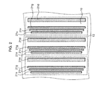
- a piece of GaN based HEMT is constituted. Further, the GaN based HEMTs as stated above are provided so as to be arranged in one direction via the element isolation insulating film 12 as illustrated in FIG. 2 . A region surrounded by the element isolation insulating film 12 is an element region 10. The GaN based HEMTs may be provided so as to be arranged in two directions via the element isolation insulating film 12.
- the i-GaN layer 5 functions as an electron transit layer and the n-AlGaN layer 6 functions as an electron supply layer.
- the i-AlN layer 2 functions as an insulating layer insulating between the substrate 1 and compound semiconductor layers including the i-GaN layer 5.
- a thickness of the i-GaN layer 5 is 0.5 ⁇ m or more so that the two-dimensional electron gas inside the i-GaN layer 5 is difficult to be affected by Fe added to the GaN layer 4.
- the two-dimensional electron gas appears at a surface layer portion of the i-GaN layer 5 as stated above, but in the present embodiment, the recess electrode 21r forming the schottky-junction with the n-GaN layer 7 is provided inside the recess portion 7a, and the recess electrode 21r is grounded. Accordingly, the two-dimensional electron gas does not exist at the surface layer portion of the i-GaN layer 5 at downward of the recess electrode 21r. Consequently, a leak current does not flow between the source electrode 21s and the drain electrode 21d under a state in which the voltage is not applied to the gate electrode 21g and an electric field seldom exists between the gate electrode 21g and the source electrode 21s. Namely, the normally-off operation is enabled.
- the current does not flow if the voltage higher than the conventional one is not applied to the gate electrode 21g, because the two-dimensional electron gas does not exist at the surface layer portion of the i-GaN layer 5 at downward of the recess electrode 21r. Namely, a threshold voltage increases.
- FIG. 3 is a band diagram illustrating an energy structure at downward of the recess electrode 21r.
- a conduction band at the recess electrode 21r side of the i-GaN layer 5 is pulled up and the two-dimensional electron gas is unable to exist there under a state in which the voltage is not applied to the gate electrode 21g.
- a predetermined voltage for example, 5V
- the conduction band becomes approximately even and the current flows. The normally-off operation is enabled as stated above.
- FIG. 4 is a graphic chart illustrating a relation between a drain current and a gate voltage in the first embodiment. This graphic chart represents a simulation result when the source electrode 21s and the recess electrode 21r are grounded and the voltage of +20 V is applied to the drain electrode 21d. As illustrated in FIG. 4 , a threshold voltage Vth exceeds 2 V, and the drain current when the voltage applied to the gate electrode 21g (gate voltage) is "0" (zero) V is "0" (zero) A/m.
- the first embodiment it is possible to obtain the high threshold voltage, and to reduce the leak current when the gate voltage is "0" (zero) V.
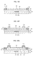
- FIG. 5A to FIG. 5I are sectional views illustrating the manufacturing method of the GaN based HEMT (compound semiconductor device) according to the first embodiment in process sequence.
- the i-AlN layer 2 is formed on the substrate 1 by, for example, a hydride vapor phase epitaxy (HVPE) method, as illustrated in FIG. 5A .
- HVPE hydride vapor phase epitaxy
- trimethylaluminum gas, ammonia gas, and HCl gas are used as source gas
- a growth pressure is set at an atmospheric pressure
- a growth speed is set at 100 ⁇ m/h.
- the i-AlN layer 3, the GaN layer 4, the i-GaN layer 5, the n-AlGaN layer 6, and the n-GaN layer 7 are sequentially formed on the i-AlN layer 2 by, for example, a metal organic chemical vapor deposition (MOCVD) method.
- MOCVD metal organic chemical vapor deposition
- the trimethylaluminum gas is used as a material of Al
- trimethylgallium gas is used as a material of Ga
- the ammonia gas is used as a material of N.
- a flow rate of the ammonia gas is set at, for example, 100 ccm to 10 LM.
- the growth pressure is set at 50 Torr to 300 Torr, a growth temperature is set at 1000°C to 1200°C.
- a growth temperature is set at 1000°C to 1200°C.
- a metal-organic material containing Fe such as ferrocene is used as a material of Fe.
- diluted SiH 4 is used as a material of Si.
- a flow rate of the diluted SiH 4 is set at, for example, a several ccm.
- the trench 11 penetrating the n-GaN layer 7 and the n-AlGaN layer 6 and reaching the i-GaN layer 5 is formed by a photolithography and an etching, as illustrated in FIG. 5B .
- the element isolation insulating film 12 is embedded in the trench 11 by, for example, a plasma CVD method.
- an element isolation region may be formed by an ion implantation of Ar or the like, instead of the formation of the trench 11 and the element isolation insulating film 12.
- the source electrode 21s and the drain electrode 21d are then formed on the n-GaN layer 7 by a lift-off method, as illustrated in FIG. 5C .
- a new resist pattern opening areas to form the source electrode 21s and the drain electrode 21d is formed, vapor depositions of Ta and Al are performed, and thereafter, Ta and Al adhered on the resist pattern are removed together with the resist pattern, to form the source electrode 21s and the drain electrode 21d.
- Thicknesses of a Ta film, an Al film are, for example, respectively approximately 20 nm, 200 nm.
- a heat treatment is performed from 400°C to 1000°C, for example, at 600°C in a nitride atmosphere to establish ohmic characteristics.
- the SiN film 22 is formed on a whole surface by, for example, a plasma CVD method, as illustrated in FIG. 5D .
- a resist pattern 31 having an opening 31a corresponding to an area to form the recess portion 7a and covering the other area is formed on the SiN film 22, as illustrated in FIG. 5E .
- an opening is formed in the SiN film 22 by etching the SiN film 22 while using the resist pattern 31 as a mask, and the recess portion 7a is formed by further etching the surface layer portion of the n-GaN layer 7, as illustrated in FIG. 5F .
- a remaining thickness of a portion where the recess portion 7a is formed of the n-GaN layer 7 is preferable to be 10 nm or less, and it is set to be, for example, approximately 5 nm to 10 nm.
- the resist pattern 31 is then removed.
- a difference between the thickness (remaining thickness) of the portion where the recess portion 7a is formed of the n-GaN layer 7 and the thickness of the other portion is 5 nm or more.
- a reason why the remaining thickness is preferable to be set at 10 nm or less is because there may be a case when the appearance of the two-dimensional electron gas cannot be suppressed enough if the remaining thickness exceeds 10 nm.
- a reason why the difference of the thicknesses is preferable to be set at 5 nm or more is because there may be a case when an effect of the recess cannot be fully obtained and the normally-off operation becomes difficult when the difference is less than 5 nm.
- a resist pattern 32 having an opening 32g corresponding to an area to form the gate electrode 21g and an opening 32a exposing the recess portion 7a, and covering the other area is formed on the SiN film 22, as illustrated in FIG. 5G .
- the gate electrode 21g and the recess electrode 21r are formed by performing vapor depositions of Ni and Au, as illustrated in FIG. 5H .
- Thicknesses of an Ni film and an Au film are, for example, respectively approximately 10 nm and 300 nm.
- the gate electrode 21g and the recess electrode 21r can be formed by a lift-off method.
- the GaN based HEMT according to the first embodiment is completed as stated above. After that, a semiconductor device in which the GaN based HEMTs are integrated is completed by forming a passivation film, external electrodes, and so on if necessary.
- the recess electrode 21r and the source electrode 21s are separated from each other, and the SiN film 22 exists therebetween, but the recess electrode 21r and the source electrode 21s may be directly in contact.
- FIG. 6 is a sectional view illustrating a structure of a GaN based HEMT (compound semiconductor device) according to the second embodiment.
- the recess electrode 21r provided in the first embodiment is not provided in the second embodiment. However, damages capturing electrons exist around the recess portion 7a.
- the other constitution is the same as the first embodiment.
- a piece of GaN based HEMT is constituted as stated above. Besides, the GaN based HEMTs are provided so as to be arranged in one direction via the element isolation insulating film 12, as illustrated in FIG. 7 . The region surrounded by the element isolation insulating film 12 is the element region 10. The GaN based HEMTs may be provided so as to be arranged in two directions via the element isolation insulating film 12.
- the two-dimensional electron gas appears at the surface layer portion of the i-GaN layer 5 in the second embodiment as stated above as same as the first embodiment, and the two-dimensional electron gas does not exist at the surface layer portion of the i-GaN layer 5 at downward of the recess portion 7a. This is because the electrons are captured by the damages around the recess portion 7a, and a balance of electric charges is established.
- FIG. 8 is a graphic chart illustrating a relation between a drain current and a gate voltage in the second embodiment. This graphic chart represents a simulation result when the source electrode 21s and the recess electrode 21r are grounded, and a voltage of +20 V is applied to the drain electrode 21d. As illustrated in FIG. 8 , the threshold voltage Vth is approximately 1 V, but the drain current when the voltage applied to the gate electrode 21g (gate voltage) is "0" (zero) V is "0" (zero) A/m.
- the leak current when the gate voltage is "0" (zero) V can also be reduced by the second embodiment.
- the structure is simple compared to the first embodiment, and therefore, a manufacture thereof is easy, and the cost can be reduced.
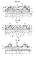
- FIG. 9A to FIG. 9C are sectional views illustrating the manufacturing method of the GaN based HEMT (compound semiconductor device) according to the second embodiment in process sequence.
- the processes up to the formation of the recess portion 7a are performed as same as the first embodiment.
- a dry etching such as a reactive ion etching (RIE) using chlorine gas is performed when the recess portion 7a is formed.
- RIE reactive ion etching
- a pressure is set to be approximately 0.1 Pa to 10 Pa (for example, 2 Pa)
- a flow rate of the chlorine gas is set to be approximately 0.1 sccm to 10 sccm (for example, 2.5 sccm).
- the n-GaN layer 7 is processed under the condition as stated above, and thereby, the recess portion 7a in which many traps capturing electrons exist therearound is formed.
- the resist pattern 31 used for the formation of the recess portion 7a is removed, and a resist pattern 42 having an opening 42g corresponding to an area to form the gate electrode 21g and covering the other area is formed on the SiN film 22, as illustrated in FIG. 9A .
- the gate electrode 21g is formed by performing the vapor deposition of Ni and Au, as illustrated in FIG. 9B .
- Thicknesses of the Ni film and Au film are, for example, respectively approximately 10 nm and 300 nm.
- the gate electrode 21g can be formed by the lift-off method as stated above.
- the GaN based HEMT according to the second embodiment is completed as stated above.
- the opening for the source electrode and the opening for the drain electrode may be formed only in the n-GaN layer 7, and the source electrode 21s and the drain electrode 21d may be formed in these openings.
- a part of the n-GaN layer 7 may remain or a part of the n-AlGaN layer 6 may be removed as for depths of these openings. Namely, the depths of the openings are not necessarily match with the thickness of the n-GaN layer 7.
- the gate electrode 21g and the n-GaN layer 7 may be directly in contact, and the gate electrode 21g may form the schottky junction with the n-GaN layer 7. Further, a recess portion may also be formed at the n-GaN layer 7 at downward of the gate electrode 21g. Namely, a gate recess structure may be taken. A depth of the recess portion as stated above may match with the thickness of the n-GaN layer 7, or the depth may either be shallower or deeper than the thickness of the n-GaN layer 7. It should be noted that it is preferable to perform the etching evenly. When the gate recess structure is taken, it is suitable for a high-speed operation because a response becomes high-speed. On the other hand, when the gate recess structure is not taken, the leak current can be suppressed more certainly. Accordingly, an adoption of the gate recess structure may be selected depending on uses thereof.
- An insulating film may exist between the recess electrode 21r and the n-GaN layer 7. Namely, it may be an MIS structure.
- an SiN film, an SiO 2 film, an HfO film, an HfNO film, an Al 2 O 3 film, a TaO film, and so on can be cited as the insulating film.
- a thickness of this insulating film is, for example, approximately 0.1 nm to 50 nm. There may be a case when the leak current increases conversely or reliability decreases because of a reason that the insulating film may be formed in island state and so on when the thickness of the insulating film is less than 0.1 nm.
- the recess electrode 21r is provided between the gate electrode 21g and the drain electrode 21d. It should be noted that there are a case when a withstand voltage is easy to become low because a high voltage is applied to the drain electrode 21d, and a case when it becomes difficult to suppress the appearance of the two-dimensional electron gas effectively, in the constitution as stated above. Accordingly, it is preferable that the recess electrode 21r is provided between the gate electrode 21g and the source electrode 21s.
- a silicon carbide (SiC) substrate, a sapphire substrate, a silicon substrate, a GaN substrate, a GaAs substrate, and so on may be used as the substrate 1.
- the substrate 1 may either be conductive, semi-insulating, or insulating.
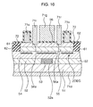
- FIG. 10 is a sectional view illustrating a structure of the GaN based HEMT (compound semiconductor device) according to the third embodiment.
- a non-doped i-AlN layer 52 having an opening 52a is formed on an n-type n-GaN layer 51.
- a thickness of the n-GaN layer 51 is approximately 0.1 ⁇ m to 100 ⁇ m (for example, 25 ⁇ m), and a thickness of the i-AlN layer 52 is approximately 0.02 ⁇ m to 20 ⁇ m.
- a planer shape of the opening 52a as a current passing area is, for example, a rectangle of which lengths in horizontal and vertical are respectively 0.5 ⁇ m and 500 ⁇ m.
- Fe which is a transition metal element, is contained in the n-GaN layer 51 as an impurity. A content ratio of Fe is approximately 1 ⁇ 10 17 cm -3 to 5 ⁇ 10 19 cm -3 .
- a GaN film 53 is formed in the opening 52a.
- a non-doped i-GaN layer 54, an n-type n-AlGaN layer 55, and an n-type n-GaN layer 56 are formed on the i-AlN layer 52 and the GaN layer 53.
- a thickness of the i-GaN layer 54 is approximately 1 ⁇ m to 2 ⁇ m.
- a thickness of the n-AlGaN layer 55 is approximately 20 nm to 30 nm.
- a thickness of the n-GaN layer 56 is approximately 3 nm to 8 nm.
- Si is contained in the n-AlGaN layer 55 and the n-GaN layer 56 as an impurity with a concentration of approximately 1 ⁇ 10 17 cm -3 to 5 ⁇ 10 19 cm -3 .
- a trench 61 for element isolation are formed in the n-AlGaN layer 55 and the n-GaN layer 56, and element isolation insulating film 62 is embedded in the trench 61.
- a source electrode 71s of which planer shape is square is formed on the n-GaN layer 56.
- the source electrode 71s may be constituted by, for example, a Ta film and an Al film formed thereon, and the source electrode 71s forms the ohmic junction with the n-GaN layer 56.
- an SiN film 72 covering the n-GaN layer 56 and the source electrode 71s is formed, and a gate electrode 71g is formed on the SiN film 72 at an area surrounded by the source electrode 71s.
- a thickness of the SiN film 72 is approximately 1 nm to 2000 nm.
- an opening is formed in the SiN film 72 between the source electrode 71s and the gate electrode 71g, and a recess portion 56a is formed at a portion exposing from the opening of the n-GaN layer 56.
- a recess electrode 71r extending upward from the recess portion 56a is formed.
- the gate electrode 71g and the recess electrode 71r may be constituted by, for example, an Ni film and an Au film formed thereon, and the recess electrode 71r forms the schottky junction with the n-GaN layer 56.
- the source electrode 71s and the recess electrode 71r are grounded.
- a drain electrode 71d is formed at a rear surface of the n-GaN layer 51.
- the drain electrode 71d may be constituted by, for example, a Ta film and an Al film formed thereon, and the drain electrode 71d forms the ohmic junction with the n-GaN layer 51.
- a piece of GaN based HEMT is constituted. Further, the GaN based HEMTs as stated above are provided so as to be arranged in one direction via the element isolation insulating film 62 as illustrated in FIG. 11 . A region surrounded by the element isolation insulating film 62 is an element region 60. The GaN based HEMTs may be provided so as to be arranged in two directions via the element isolation insulating film 62.
- the n-AlGaN layer 55 functions as an electron supplying layer supplying electrons to the i-GaN layer 54 (electron transit layer).
- a band gap of the n-AlGaN layer 55 is wide, and therefore, a deep potential well is formed in the i-GaN layer 54 at a region in the vicinity of an interface with the n-AlGaN layer 55, and two-dimensional electron gas (2DEG) appears there.
- the i-AlN layer 52 functions as an insulating layer insulating between a compound semiconductor layer including the i-GaN layer 54, and the n-GaN layer 51 and the drain electrode 71d.
- a thickness of the i-GaN layer 54 is 0.5 ⁇ m or more so that the two-dimensional electron gas inside the i-GaN layer 54 is difficult to be affected by Fe added to the n-GaN layer 51.
- the two-dimensional electron gas appears at a surface layer portion of the i-GaN layer 54, but in the present embodiment, the recess electrode 71r which forms the schottky junction with the n-GaN layer 56 is provided in the recess portion 56a, and the recess electrode 71r is grounded. Accordingly, the two-dimensional electron gas does not exist at the surface layer portion of the i-GaN layer 54 at downward of the recess electrode 71r resulting from the same reason as the first embodiment.
- a leak current does not flow between the source electrode 71s and the drain electrode 71d under a state in which the voltage is not applied to the gate electrode 71g and an electric field seldom exists between the gate electrode 71g and the source electrode 71s. Namely, the normally-off operation is enabled. Besides, the current does not flow if the voltage higher than the conventional one is not applied to the gate electrode 71g, because the two-dimensional electron gas does not exist at the surface layer portion of the i-GaN layer 54 at downward of the recess electrode 71r. Namely, the threshold voltage increases resulting from the same reason as the first embodiment.
- the third embodiment it is possible to obtain the high threshold voltage, and to reduce the leak current when the gate voltage is "0" (zero) V, in addition that the normally-off operation is enabled also in the vertical structure.
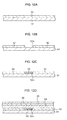
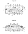
- FIG. 12A to FIG. 12N are sectional views illustrating the manufacturing method of the GaN based HEMT (compound semiconductor device) according to the third embodiment in process sequence.
- the i-AlN layer 52 is formed on the n-GaN layer 51 by an HVPE method, as illustrated in FIG. 12A .
- the opening 52a is formed at the i-AlN layer 52, as illustrated in FIG. 12B .
- a resist pattern exposing an area to form the opening 52a is formed on the i-AlN layer 52, and the i-AIN layer 52 is etched by using this resist pattern as a mask. After that, the resist pattern is removed.
- the GaN layer 53 is formed in the opening 52a by, for example, an MOCVD method, as illustrated in FIG. 12C .
- the i-GaN layer 54, the n-AlGaN layer 55, and the n-GaN layer 56 are formed in this sequence on the i-AlN layer 52 and the GaN layer 53 by, for example, an MOCVD method, as illustrated in FIG. 12D .
- the trench 61 penetrating the n-GaN layer 56 and the n-AlGaN layer 55 and reaching the i-GaN layer 54 is formed by a photolithography and an etching, as illustrated in FIG. 12E .
- the element isolation insulating film 62 is embedded inside the trench 61 by, for example, a plasma CVD method.
- an element isolation region may be formed by an ion implantation such as Ar, instead of the formation of the trench 61 and the element isolation insulating film 62.
- the source electrode 71s is then formed on the n-GaN layer 56 by a lift-off method, as illustrated in FIG. 12F .
- a new resist pattern opening an area to form the source electrode 71s is formed, vapor depositions of Ta and Al are performed, and thereafter, Ta and Al adhered on the resist pattern are removed together with the resist pattern.
- Thicknesses of a Ta film, an Al film are set to be, for example, respectively approximately 20 nm, 200 nm.
- the heat treatment is performed from 400°C to 1000°C, for example, at 600°C in a nitride atmosphere to establish the ohmic characteristics.
- the SiN film 72 is formed on a whole surface by, for example, a plasma CVD method, as illustrated in FIG. 12G .
- a resist pattern 81 having an opening 81a corresponding to an area to form the recess portion 56a and covering the other area is formed on the SiN film 72, as illustrated in FIG. 12H .
- an opening is formed in the SiN film 72 by etching the SiN film 72 with using the resist pattern 81 as a mask, as illustrated in FIG. 12I , and the recess portion 56a is formed by etching the surface layer portion of the n-GaN layer 56.
- a remaining thickness of a portion where the recess portion 56a is formed of the n-GaN layer 56 is preferable to be 10 nm or less, and it is set to be, for example, approximately 5 nm to 10 nm.
- the resist pattern 81 is then removed.
- a resist pattern 82 having an opening 82g corresponding to an area to form the gate electrode 71g and an opening 82a exposing the recess portion 56a and covering the other area is formed on the SiN film 72, as illustrated in FIG. 12J .
- the gate electrode 71g and the recess electrode 71r are formed by performing vapor depositions of Ni and Au, as illustrated in FIG. 12K .
- Thicknesses of an Ni film and an Au film are, for example, respectively approximately 10 nm and 300 nm.
- the gate electrode 71g and the recess electrode 71r can be formed by a lift-off method.
- a surface protecting layer 83 is formed on a whole surface at a front surface side of the n-GaN layer 51, as illustrated in FIG. 12M , and the front-and-rear of the n-GaN layer 51 are reversed.
- the drain electrode 71d is formed on the whole surface of the rear surface of the n-GaN layer 51.
- the GaN based HEMT according to the third embodiment is completed as stated above. After that, a semiconductor device in which the GaN based HEMTs are integrated is completed by forming the passivation film, external electrodes, and so on if necessary.
- an n-type conductive GaN substrate may be used as the n-GaN layer 51 in the third embodiment.
- the n-GaN layer 51 may be formed on a conductive substrate.
- the opening for the source electrode is formed only in the n-GaN layer 56, and the source electrode 71s may be formed in the opening.
- a part of the n-GaN layer 56 may remain or a part of the n-AlGaN layer 55 may be removed, as for a depth of the opening. Namely, the depth of the opening is not necessarily match with the thickness of the n-GaN layer 56.
- the gate electrode 71g and the n-GaN layer 56 may be directly in contact, and the gate electrode 71g may form the schottky junction with the n-GaN layer 56. Further, a recess portion may be formed at the n-GaN layer 56 also at downward of the gate electrode 71g. Namely, the gate recess structure may be taken. A depth of the recess portion as stated above may match with the thickness of the n-GaN layer 56, or the depth may be shallower than the thickness of the n-GaN layer 56. It should be noted that it is preferable to perform the etching evenly. When the gate recess structure is taken, it is suitable for a high-speed operation because a response becomes high-speed. On the other hand, when the gate recess structure is not taken, the leak current can be suppressed more certainly. Accordingly, the adoption of the gate recess structure may be selected depending on uses thereof.
- the structures of the gate electrode, the source electrode, the drain electrode and the recess electrode are not limited to the ones in the above-stated embodiments.
- these electrodes may be constituted by a single layer.
- the formation method thereof is not limited to the lift-off method.
- the heat treatment after the formations of the source electrode and the drain electrode may not be performed as long as the ohmic characteristics can be obtained. The heat treatment may be performed for the gate electrode and the recess electrode.
- Any one kind or a combination of two kinds or more from among gold, nickel, platinum, copper, tungsten nitride, titanium nitride, palladium, cobalt, rhodium, rhenium, and iridium can be cited as materials of the gate electrode and the recess electrode.
- each layer is not limited to the ones in the above-stated embodiments.
- the recess electrode is not necessarily connected to the source electrode, and also, it is not necessary to be grounded as long as the electric potential different from the gate electrode is supplied thereto.
- an insulating film of which relative dielectric constant is three or less is provided between the source electrode and the gate electrode.
- a porous SiOH film, a carbon fluoride film, an organic silica film, and so on can be cited as the insulating film as stated above.
Landscapes
- Junction Field-Effect Transistors (AREA)
Abstract
Description
- The embodiments discussed herein are directed to a compound semiconductor device and a manufacturing method thereof.
- Conventionally, a study relating to a high electron mobility transistor (HEMT) in which an AlGaN layer and a GaN layer are formed over a substrate by crystal growth, and the GaN layer functions as an electron transit layer has been performed. A band gap of GaN is 3.4 eV, and it is larger than a band gap of GaAs (1.4 eV). Accordingly, a withstand voltage of a GaN based HEMT is high, and it is expectable as a high withstand voltage electronic device for automobiles and so on.
- Besides, there are a horizontal structure, in which a source and a drain are disposed in parallel to a surface of a substrate, and a vertical structure, in which a source and a drain are disposed perpendicularly to a surface of a substrate, as structures of the GaN based HEMT.
- In the GaN based HEMT, a current flows in a channel because two-dimensional electron gas (2DEG) resulting from a difference between lattice constants exists at the channel positioning in a vicinity of a gate electrode, caused by a structure of the GaN based HEMT even in a case when a voltage is not applied to the gate electrode. Namely, a normally-on operation is performed. On the other hand, it is also conceivable that current flows between the source and the drain when "0" (zero) V is unintentionally applied to the gate electrode, when a power is turned on, when the gate electrode is broken, or the like. Accordingly, a normally-off operation of the GaN based HEMT is desired from a point of view of fail-safe.
- The normally-off operation is enabled by a structure in which a recess is formed at a compound semiconductor layer positioning directly below the gate electrode (gate recess structure) as for the GaN based HEMT having the horizontal structure.
- However, in the gate recess structure as stated above, the normally-off operation is enabled, but a threshold voltage is 1 V or less, and a leak current may be generated even though the gate voltage is "0" (zero) V. Besides, it is difficult to use it for an electronic device to which a high voltage is applied if the threshold voltage is 1 V or less, because noise increases and operations become unstable when the high voltage is applied. It is possible to increase the threshold voltage by changing a material from the GaN based material, but it may result in a case that a sufficient current cannot be obtained, or it becomes easy to break only by changing the material.
- On the other hand, a study has also been performed to enable the normally-off operation in the GaN based HEMT having the vertical structure, but mass production thereof is difficult by either method.
- The following are examples of related art of the present invention: Japanese Laid-open Patent Publication No.
2006-140368 WO 2006/001369 ; and Japanese Journal of Applied Physics vol. 46, No. 21, 2007, pp. L503-L505. - It is desirable to provide a compound semiconductor device and a manufacturing method thereof capable of reducing a leak current at a power-off time, and preferably obtaining a high threshold voltage.
- According to embodiments of an aspect of the invention, a first compound semiconductor device includes: an electron transit layer; a compound semiconductor layer formed over the electron transit layer; and a source electrode, a drain electrode and a gate electrode formed over the compound semiconductor layer. A recess portion is formed inside an area between the source electrode and the drain electrode of the compound semiconductor layer and at a portion separating from the gate electrode.
- According to embodiments of another aspect, a second compound semiconductor device, includes: an electron transit layer; a compound semiconductor layer formed over the electron transit layer; a gate electrode and a source electrode formed over the compound semiconductor layer, and a drain electrode formed below the electron transit layer. A recess portion is formed inside an area between the source electrode and the gate electrode of the compound semiconductor layer.
- Preferred features of the present invention will now be described, purely by way of example, with reference to the accompanying drawings, in which:-
-
FIG. 1 is a sectional view illustrating a structure of a GaN based HEMT (compound semiconductor device) according to a first embodiment; -
FIG. 2 is a layout view illustrating the structure of the GaN based HEMT according to the first embodiment; -
FIG. 3 is a band diagram illustrating an energy structure at downward of arecess electrode 21r; -
FIG. 4 is a graphic chart illustrating a relation between a drain current and a gate voltage in the first embodiment; -
FIG. 5A to FIG. 5I are sectional views illustrating a manufacturing method of the GaN based HEMT according to the first embodiment in process sequence; -
FIG. 6 is a sectional view illustrating a structure of a GaN based HEMT (compound semiconductor device) according to a second embodiment; -
FIG. 7 is a layout view illustrating the structure of the GaN based HEMT according to the second embodiment; -
FIG. 8 is a graphic chart illustrating a relation between a drain current and a gate voltage in the second embodiment; -
FIG. 9A to FIG. 9C are sectional views illustrating a manufacturing method of the GaN based HEMT according to the second embodiment in process sequence; -
FIG. 10 is a sectional view illustrating a structure of a GaN based HEMT (compound semiconductor device) according to a third embodiment; -
FIG. 11 is a layout view illustrating the structure of the GaN based HEMT according to the third embodiment; -
FIG. 12A to FIG. 12N are sectional views illustrating a manufacturing method of the GaN based HEMT according to the third embodiment in process sequence. - First, a first embodiment is described.
FIG. 1 is a sectional view illustrating a structure of a GaN based HEMT (compound semiconductor device) according to the first embodiment. - In the first embodiment, an undoped i-
AlN layer 2 with a thickness of approximately 1 µm to 100 µm (for example, 25 µm) is formed on asubstrate 1 such as an n-type conductive single-crystal SiC substrate. Relatively large concaves and convexes exist at a surface of the i-AlN layer 2. An undoped i-AlN layer 3 of which thickness is 100 nm or less (for example, 20 nm to 50 nm) is formed on the i-AlN layer 2. AGaN layer 4 of which thickness is approximately 0.1 µm to 10 µm (for example, 0.5 µm) is formed on the i-AlN layer 3. Fe, which is a transition metal element, is contained in theGaN layer 4 as an impurity. A content ratio of Fe is, for example, approximately 1 × 1018 cm-3 to 1 × 1020 cm-3. The thickness of theGaN layer 4 is approximately 0.1 µm to 10 µm, and therefore, a surface of theGaN layer 4 is flat even though the concaves and convexes exist at the surface of the i-AlN layer 2. An undoped i-GaN layer 5 of which thickness is approximately 0.1 µm to 10 µm is formed on theGaN layer 4. Fe is not contained in the i-GaN layer 5. An n-type n-AlGaN layer 6 of which thickness is approximately 5 nm to 50 nm is formed on the i-GaN layer 5. An n-type n-GaN layer 7 of which thickness is approximately 0.1 nm to 10 nm is formed on the n-AlGaN layer 6. For example, Si is contained in the n-AlGaN layer 6 and the n-GaN layer 7 as an impurity with a concentration of approximately 5 × 1017 cm-3 to 5 × 1019 cm-3. - A
trench 11 for element isolation is formed in the n-AlGaN layer 6 and the n-GaN layer 7, and an elementisolation insulating film 12 is embedded in thetrench 11. Asource electrode 21s and adrain electrode 21d are formed on the n-GaN layer 7. Thesource electrode 21s and thedrain electrode 21d may be constituted by, for example, a Ta film and an A1 film formed thereon, and thesource electrode 21s and thedrain electrode 21d form an ohmic junction with the n-GaN layer 7. - Further, an
SiN film 22 covering the n-GaN layer 7, thesource electrode 21s and thedrain electrode 21d is formed, and agate electrode 21g is formed on theSiN film 22 between thesource electrode 21s and thedrain electrode 21d. A thickness of theSiN film 22 is approximately 10 nm to 2000 nm. Besides, an opening is formed in the SiNfilm 22 between thesource electrode 21s and thegate electrode 21g, and arecess portion 7a is formed at a portion exposing from this opening of the n-GaN layer 7. Therecess portion 7a may either stop at the n-GaN layer 7 or extend up to the n-AlGaN layer 6. Arecess electrode 21r extending upward from therecess portion 7a is formed. Thegate electrode 21g and therecess electrode 21r may be constituted by, for example, an Ni film and an Au film formed thereon, and therecess electrode 21r forms a schottky junction with the n-GaN layer 7. - Besides, the
source electrode 21s and therecess electrode 21r are grounded. - As stated above, a piece of GaN based HEMT is constituted. Further, the GaN based HEMTs as stated above are provided so as to be arranged in one direction via the element
isolation insulating film 12 as illustrated inFIG. 2 . A region surrounded by the elementisolation insulating film 12 is anelement region 10. The GaN based HEMTs may be provided so as to be arranged in two directions via the elementisolation insulating film 12. - In the first embodiment as stated above, electrons are induced in a vicinity of an interface between the i-
GaN layer 5 and the n-AlGaN layer 6 by a piezoelectric effect resulting from a lattice mismatch. As a result, two-dimensional electron gas (2DEG) appears, and this portion functions as an electron transit layer and the n-AlGaN layer 6 functions as an electron supply layer. Besides, the i-AlN layer 2 functions as an insulating layer insulating between thesubstrate 1 and compound semiconductor layers including the i-GaN layer 5. Incidentally, it is desirable that a thickness of the i-GaN layer 5 is 0.5 µm or more so that the two-dimensional electron gas inside the i-GaN layer 5 is difficult to be affected by Fe added to theGaN layer 4. - The two-dimensional electron gas appears at a surface layer portion of the i-
GaN layer 5 as stated above, but in the present embodiment, therecess electrode 21r forming the schottky-junction with the n-GaN layer 7 is provided inside therecess portion 7a, and therecess electrode 21r is grounded. Accordingly, the two-dimensional electron gas does not exist at the surface layer portion of the i-GaN layer 5 at downward of therecess electrode 21r. Consequently, a leak current does not flow between thesource electrode 21s and thedrain electrode 21d under a state in which the voltage is not applied to thegate electrode 21g and an electric field seldom exists between thegate electrode 21g and thesource electrode 21s. Namely, the normally-off operation is enabled. Besides, the current does not flow if the voltage higher than the conventional one is not applied to thegate electrode 21g, because the two-dimensional electron gas does not exist at the surface layer portion of the i-GaN layer 5 at downward of therecess electrode 21r. Namely, a threshold voltage increases. -
FIG. 3 is a band diagram illustrating an energy structure at downward of therecess electrode 21r.
As illustrated inFIG. 3 , a conduction band at therecess electrode 21r side of the i-GaN layer 5 is pulled up and the two-dimensional electron gas is unable to exist there under a state in which the voltage is not applied to thegate electrode 21g. On the other hand, when a predetermined voltage (for example, 5V) is applied to thegate electrode 21g, the conduction band becomes approximately even and the current flows. The normally-off operation is enabled as stated above. -
FIG. 4 is a graphic chart illustrating a relation between a drain current and a gate voltage in the first embodiment. This graphic chart represents a simulation result when thesource electrode 21s and therecess electrode 21r are grounded and the voltage of +20 V is applied to thedrain electrode 21d. As illustrated inFIG. 4 , a threshold voltage Vth exceeds 2 V, and the drain current when the voltage applied to thegate electrode 21g (gate voltage) is "0" (zero) V is "0" (zero) A/m. - As stated above, according to the first embodiment, it is possible to obtain the high threshold voltage, and to reduce the leak current when the gate voltage is "0" (zero) V.
- Next, a manufacturing method of the GaN based HEMT (compound semiconductor device) according to the first embodiment is described.
FIG. 5A to FIG. 5I are sectional views illustrating the manufacturing method of the GaN based HEMT (compound semiconductor device) according to the first embodiment in process sequence. - In the first embodiment, first, the i-
AlN layer 2 is formed on thesubstrate 1 by, for example, a hydride vapor phase epitaxy (HVPE) method, as illustrated inFIG. 5A . At this time, for example, trimethylaluminum gas, ammonia gas, and HCl gas are used as source gas, a growth pressure is set at an atmospheric pressure, and a growth speed is set at 100 µm/h. - Next, the i-
AlN layer 3, theGaN layer 4, the i-GaN layer 5, the n-AlGaN layer 6, and the n-GaN layer 7 are sequentially formed on the i-AlN layer 2 by, for example, a metal organic chemical vapor deposition (MOCVD) method. When these layers are formed, the trimethylaluminum gas is used as a material of Al, trimethylgallium gas is used as a material of Ga, and the ammonia gas is used as a material of N. Besides, a flow rate of the ammonia gas is set at, for example, 100 ccm to 10 LM. Besides, the growth pressure is set at 50 Torr to 300 Torr, a growth temperature is set at 1000°C to 1200°C. When theGaN layer 4 containing Fe is formed, for example, a metal-organic material containing Fe such as ferrocene is used as a material of Fe. Besides, when the n-AlGaN layer 6 and the n-GaN layer 7 are formed, for example, diluted SiH4 is used as a material of Si. A flow rate of the diluted SiH4 is set at, for example, a several ccm. - Subsequently, the
trench 11 penetrating the n-GaN layer 7 and the n-AlGaN layer 6 and reaching the i-GaN layer 5 is formed by a photolithography and an etching, as illustrated inFIG. 5B . Next, the elementisolation insulating film 12 is embedded in thetrench 11 by, for example, a plasma CVD method. Incidentally, an element isolation region may be formed by an ion implantation of Ar or the like, instead of the formation of thetrench 11 and the elementisolation insulating film 12. - The
source electrode 21s and thedrain electrode 21d are then formed on the n-GaN layer 7 by a lift-off method, as illustrated inFIG. 5C . A new resist pattern opening areas to form thesource electrode 21s and thedrain electrode 21d is formed, vapor depositions of Ta and Al are performed, and thereafter, Ta and Al adhered on the resist pattern are removed together with the resist pattern, to form thesource electrode 21s and thedrain electrode 21d. Thicknesses of a Ta film, an Al film are, for example, respectively approximately 20 nm, 200 nm. A heat treatment is performed from 400°C to 1000°C, for example, at 600°C in a nitride atmosphere to establish ohmic characteristics. - Next, the
SiN film 22 is formed on a whole surface by, for example, a plasma CVD method, as illustrated inFIG. 5D . - After that, a resist
pattern 31 having anopening 31a corresponding to an area to form therecess portion 7a and covering the other area is formed on theSiN film 22, as illustrated inFIG. 5E . - Subsequently, an opening is formed in the
SiN film 22 by etching theSiN film 22 while using the resistpattern 31 as a mask, and therecess portion 7a is formed by further etching the surface layer portion of the n-GaN layer 7, as illustrated inFIG. 5F . A remaining thickness of a portion where therecess portion 7a is formed of the n-GaN layer 7 is preferable to be 10 nm or less, and it is set to be, for example, approximately 5 nm to 10 nm. The resistpattern 31 is then removed. Besides, it is preferable that a difference between the thickness (remaining thickness) of the portion where therecess portion 7a is formed of the n-GaN layer 7 and the thickness of the other portion is 5 nm or more. A reason why the remaining thickness is preferable to be set at 10 nm or less is because there may be a case when the appearance of the two-dimensional electron gas cannot be suppressed enough if the remaining thickness exceeds 10 nm. Besides, a reason why the difference of the thicknesses is preferable to be set at 5 nm or more is because there may be a case when an effect of the recess cannot be fully obtained and the normally-off operation becomes difficult when the difference is less than 5 nm. - Next, a resist
pattern 32 having anopening 32g corresponding to an area to form thegate electrode 21g and anopening 32a exposing therecess portion 7a, and covering the other area is formed on theSiN film 22, as illustrated inFIG. 5G . - After that, the
gate electrode 21g and therecess electrode 21r are formed by performing vapor depositions of Ni and Au, as illustrated inFIG. 5H . Thicknesses of an Ni film and an Au film are, for example, respectively approximately 10 nm and 300 nm. - Subsequently, Ni and Au adhered on the resist
pattern 32 are removed together with the resistpattern 32, as illustrated inFIG. 5I . Thus, thegate electrode 21g and therecess electrode 21r can be formed by a lift-off method. - Next, a wiring to ground the
source electrode 21s and therecess electrode 21r, and so on are formed. - The GaN based HEMT according to the first embodiment is completed as stated above. After that, a semiconductor device in which the GaN based HEMTs are integrated is completed by forming a passivation film, external electrodes, and so on if necessary.
- In the first embodiment, the
recess electrode 21r and thesource electrode 21s are separated from each other, and theSiN film 22 exists therebetween, but therecess electrode 21r and thesource electrode 21s may be directly in contact. - Next, a second embodiment is described.
FIG. 6 is a sectional view illustrating a structure of a GaN based HEMT (compound semiconductor device) according to the second embodiment. - The
recess electrode 21r provided in the first embodiment is not provided in the second embodiment. However, damages capturing electrons exist around therecess portion 7a. The other constitution is the same as the first embodiment. - A piece of GaN based HEMT is constituted as stated above. Besides, the GaN based HEMTs are provided so as to be arranged in one direction via the element
isolation insulating film 12, as illustrated inFIG. 7 . The region surrounded by the elementisolation insulating film 12 is theelement region 10. The GaN based HEMTs may be provided so as to be arranged in two directions via the elementisolation insulating film 12. - The two-dimensional electron gas appears at the surface layer portion of the i-
GaN layer 5 in the second embodiment as stated above as same as the first embodiment, and the two-dimensional electron gas does not exist at the surface layer portion of the i-GaN layer 5 at downward of therecess portion 7a. This is because the electrons are captured by the damages around therecess portion 7a, and a balance of electric charges is established. -
FIG. 8 is a graphic chart illustrating a relation between a drain current and a gate voltage in the second embodiment. This graphic chart represents a simulation result when thesource electrode 21s and therecess electrode 21r are grounded, and a voltage of +20 V is applied to thedrain electrode 21d. As illustrated inFIG. 8 , the threshold voltage Vth is approximately 1 V, but the drain current when the voltage applied to thegate electrode 21g (gate voltage) is "0" (zero) V is "0" (zero) A/m. - As stated above, the leak current when the gate voltage is "0" (zero) V can also be reduced by the second embodiment. Besides, the structure is simple compared to the first embodiment, and therefore, a manufacture thereof is easy, and the cost can be reduced.
- Next, a manufacturing method of the GaN based HEMT (compound semiconductor device) according to the second embodiment is described.
FIG. 9A to FIG. 9C are sectional views illustrating the manufacturing method of the GaN based HEMT (compound semiconductor device) according to the second embodiment in process sequence. - In the second embodiment, at first, the processes up to the formation of the
recess portion 7a (FIG. 5F ) are performed as same as the first embodiment. Incidentally, for example, a dry etching such as a reactive ion etching (RIE) using chlorine gas is performed when therecess portion 7a is formed. Besides, a pressure is set to be approximately 0.1 Pa to 10 Pa (for example, 2 Pa), and a flow rate of the chlorine gas is set to be approximately 0.1 sccm to 10 sccm (for example, 2.5 sccm). The n-GaN layer 7 is processed under the condition as stated above, and thereby, therecess portion 7a in which many traps capturing electrons exist therearound is formed. - Next, the resist
pattern 31 used for the formation of therecess portion 7a is removed, and a resistpattern 42 having anopening 42g corresponding to an area to form thegate electrode 21g and covering the other area is formed on theSiN film 22, as illustrated inFIG. 9A . - After that, the
gate electrode 21g is formed by performing the vapor deposition of Ni and Au, as illustrated inFIG. 9B . Thicknesses of the Ni film and Au film are, for example, respectively approximately 10 nm and 300 nm. - Subsequently, Ni and Au adhered on the resist
pattern 42 are removed together with the resistpattern 42, as illustrated inFIG. 9C . Thegate electrode 21g can be formed by the lift-off method as stated above. - The GaN based HEMT according to the second embodiment is completed as stated above.
- In the first and second embodiments, the opening for the source electrode and the opening for the drain electrode may be formed only in the n-
GaN layer 7, and thesource electrode 21s and thedrain electrode 21d may be formed in these openings. A part of the n-GaN layer 7 may remain or a part of the n-AlGaN layer 6 may be removed as for depths of these openings. Namely, the depths of the openings are not necessarily match with the thickness of the n-GaN layer 7. - Besides, the
gate electrode 21g and the n-GaN layer 7 may be directly in contact, and thegate electrode 21g may form the schottky junction with the n-GaN layer 7. Further, a recess portion may also be formed at the n-GaN layer 7 at downward of thegate electrode 21g. Namely, a gate recess structure may be taken. A depth of the recess portion as stated above may match with the thickness of the n-GaN layer 7, or the depth may either be shallower or deeper than the thickness of the n-GaN layer 7. It should be noted that it is preferable to perform the etching evenly. When the gate recess structure is taken, it is suitable for a high-speed operation because a response becomes high-speed. On the other hand, when the gate recess structure is not taken, the leak current can be suppressed more certainly. Accordingly, an adoption of the gate recess structure may be selected depending on uses thereof. - An insulating film may exist between the
recess electrode 21r and the n-GaN layer 7. Namely, it may be an MIS structure. For example, an SiN film, an SiO2 film, an HfO film, an HfNO film, an Al2O3 film, a TaO film, and so on can be cited as the insulating film. A thickness of this insulating film is, for example, approximately 0.1 nm to 50 nm. There may be a case when the leak current increases conversely or reliability decreases because of a reason that the insulating film may be formed in island state and so on when the thickness of the insulating film is less than 0.1 nm. There may be a case when the appearance of the two-dimensional electron gas cannot be fully suppressed because a distance between therecess electrode 21r and the n-AlGaN layer 6 becomes too large when the thickness of the insulating film exceeds 50 nm. - It is also possible to suppress the appearance of the two-dimensional electron gas even when the
recess electrode 21r is provided between thegate electrode 21g and thedrain electrode 21d. It should be noted that there are a case when a withstand voltage is easy to become low because a high voltage is applied to thedrain electrode 21d, and a case when it becomes difficult to suppress the appearance of the two-dimensional electron gas effectively, in the constitution as stated above. Accordingly, it is preferable that therecess electrode 21r is provided between thegate electrode 21g and thesource electrode 21s. - A silicon carbide (SiC) substrate, a sapphire substrate, a silicon substrate, a GaN substrate, a GaAs substrate, and so on may be used as the
substrate 1. Thesubstrate 1 may either be conductive, semi-insulating, or insulating. - Next, a third embodiment is described. Structures of the GaN based HEMTs according to the first and second embodiments are horizontal structures, but a structure of a GaN based HEMT according to the third embodiment is a vertical structure.
FIG. 10 is a sectional view illustrating a structure of the GaN based HEMT (compound semiconductor device) according to the third embodiment. - In the third embodiment, a non-doped i-
AlN layer 52 having anopening 52a is formed on an n-type n-GaN layer 51. A thickness of the n-GaN layer 51 is approximately 0.1 µm to 100 µm (for example, 25 µm), and a thickness of the i-AlN layer 52 is approximately 0.02 µm to 20 µm. A planer shape of theopening 52a as a current passing area is, for example, a rectangle of which lengths in horizontal and vertical are respectively 0.5 µm and 500 µm. Fe, which is a transition metal element, is contained in the n-GaN layer 51 as an impurity. A content ratio of Fe is approximately 1 × 1017 cm-3 to 5 × 1019 cm-3. AGaN film 53 is formed in theopening 52a. - Further, a non-doped i-
GaN layer 54, an n-type n-AlGaN layer 55, and an n-type n-GaN layer 56 are formed on the i-AlN layer 52 and theGaN layer 53. A thickness of the i-GaN layer 54 is approximately 1 µm to 2 µm. A thickness of the n-AlGaN layer 55 is approximately 20 nm to 30 nm. A thickness of the n-GaN layer 56 is approximately 3 nm to 8 nm. For example, Si is contained in the n-AlGaN layer 55 and the n-GaN layer 56 as an impurity with a concentration of approximately 1 × 1017 cm-3 to 5 × 1019 cm-3. - A
trench 61 for element isolation are formed in the n-AlGaN layer 55 and the n-GaN layer 56, and elementisolation insulating film 62 is embedded in thetrench 61. Asource electrode 71s of which planer shape is square is formed on the n-GaN layer 56. Thesource electrode 71s may be constituted by, for example, a Ta film and an Al film formed thereon, and thesource electrode 71s forms the ohmic junction with the n-GaN layer 56. - Further, an
SiN film 72 covering the n-GaN layer 56 and thesource electrode 71s is formed, and agate electrode 71g is formed on theSiN film 72 at an area surrounded by thesource electrode 71s. A thickness of theSiN film 72 is approximately 1 nm to 2000 nm. Besides, an opening is formed in theSiN film 72 between thesource electrode 71s and thegate electrode 71g, and arecess portion 56a is formed at a portion exposing from the opening of the n-GaN layer 56. Arecess electrode 71r extending upward from therecess portion 56a is formed. Thegate electrode 71g and therecess electrode 71r may be constituted by, for example, an Ni film and an Au film formed thereon, and therecess electrode 71r forms the schottky junction with the n-GaN layer 56. - Besides, the
source electrode 71s and therecess electrode 71r are grounded. - Further, a
drain electrode 71d is formed at a rear surface of the n-GaN layer 51. Thedrain electrode 71d may be constituted by, for example, a Ta film and an Al film formed thereon, and thedrain electrode 71d forms the ohmic junction with the n-GaN layer 51. - As stated above, a piece of GaN based HEMT is constituted. Further, the GaN based HEMTs as stated above are provided so as to be arranged in one direction via the element
isolation insulating film 62 as illustrated inFIG. 11 . A region surrounded by the elementisolation insulating film 62 is anelement region 60. The GaN based HEMTs may be provided so as to be arranged in two directions via the elementisolation insulating film 62. - In the third embodiment as stated above, the n-
AlGaN layer 55 functions as an electron supplying layer supplying electrons to the i-GaN layer 54 (electron transit layer). A band gap of the n-AlGaN layer 55 is wide, and therefore, a deep potential well is formed in the i-GaN layer 54 at a region in the vicinity of an interface with the n-AlGaN layer 55, and two-dimensional electron gas (2DEG) appears there. Besides, the i-AlN layer 52 functions as an insulating layer insulating between a compound semiconductor layer including the i-GaN layer 54, and the n-GaN layer 51 and thedrain electrode 71d. Incidentally, it is desirable that a thickness of the i-GaN layer 54 is 0.5 µm or more so that the two-dimensional electron gas inside the i-GaN layer 54 is difficult to be affected by Fe added to the n-GaN layer 51. - As stated above, the two-dimensional electron gas appears at a surface layer portion of the i-
GaN layer 54, but in the present embodiment, therecess electrode 71r which forms the schottky junction with the n-GaN layer 56 is provided in therecess portion 56a, and therecess electrode 71r is grounded. Accordingly, the two-dimensional electron gas does not exist at the surface layer portion of the i-GaN layer 54 at downward of therecess electrode 71r resulting from the same reason as the first embodiment. Consequently, a leak current does not flow between thesource electrode 71s and thedrain electrode 71d under a state in which the voltage is not applied to thegate electrode 71g and an electric field seldom exists between thegate electrode 71g and thesource electrode 71s. Namely, the normally-off operation is enabled. Besides, the current does not flow if the voltage higher than the conventional one is not applied to thegate electrode 71g, because the two-dimensional electron gas does not exist at the surface layer portion of the i-GaN layer 54 at downward of therecess electrode 71r. Namely, the threshold voltage increases resulting from the same reason as the first embodiment. - According to the third embodiment, it is possible to obtain the high threshold voltage, and to reduce the leak current when the gate voltage is "0" (zero) V, in addition that the normally-off operation is enabled also in the vertical structure.
- Next, a manufacturing method of the GaN based HEMT (compound semiconductor device) according to the third embodiment is described.
FIG. 12A to FIG. 12N are sectional views illustrating the manufacturing method of the GaN based HEMT (compound semiconductor device) according to the third embodiment in process sequence. - At first, the i-
AlN layer 52 is formed on the n-GaN layer 51 by an HVPE method, as illustrated inFIG. 12A . - Next, the
opening 52a is formed at the i-AlN layer 52, as illustrated inFIG. 12B . As for the formation of theopening 52a, for example, a resist pattern exposing an area to form theopening 52a is formed on the i-AlN layer 52, and the i-AIN layer 52 is etched by using this resist pattern as a mask. After that, the resist pattern is removed. - After that, the
GaN layer 53 is formed in theopening 52a by, for example, an MOCVD method, as illustrated inFIG. 12C . - Subsequently, the i-
GaN layer 54, the n-AlGaN layer 55, and the n-GaN layer 56 are formed in this sequence on the i-AlN layer 52 and theGaN layer 53 by, for example, an MOCVD method, as illustrated inFIG. 12D . - Next, the
trench 61 penetrating the n-GaN layer 56 and the n-AlGaN layer 55 and reaching the i-GaN layer 54 is formed by a photolithography and an etching, as illustrated inFIG. 12E . After that, the elementisolation insulating film 62 is embedded inside thetrench 61 by, for example, a plasma CVD method. Incidentally, an element isolation region may be formed by an ion implantation such as Ar, instead of the formation of thetrench 61 and the elementisolation insulating film 62. - The
source electrode 71s is then formed on the n-GaN layer 56 by a lift-off method, as illustrated inFIG. 12F . In the formation of thesource electrode 71s, a new resist pattern opening an area to form thesource electrode 71s is formed, vapor depositions of Ta and Al are performed, and thereafter, Ta and Al adhered on the resist pattern are removed together with the resist pattern. Thicknesses of a Ta film, an Al film are set to be, for example, respectively approximately 20 nm, 200 nm. The heat treatment is performed from 400°C to 1000°C, for example, at 600°C in a nitride atmosphere to establish the ohmic characteristics. - Next, the
SiN film 72 is formed on a whole surface by, for example, a plasma CVD method, as illustrated inFIG. 12G . - After that, a resist
pattern 81 having anopening 81a corresponding to an area to form therecess portion 56a and covering the other area is formed on theSiN film 72, as illustrated inFIG. 12H . - Subsequently, an opening is formed in the
SiN film 72 by etching theSiN film 72 with using the resistpattern 81 as a mask, as illustrated inFIG. 12I , and therecess portion 56a is formed by etching the surface layer portion of the n-GaN layer 56. A remaining thickness of a portion where therecess portion 56a is formed of the n-GaN layer 56 is preferable to be 10 nm or less, and it is set to be, for example, approximately 5 nm to 10 nm. The resistpattern 81 is then removed. - Next, a resist
pattern 82 having anopening 82g corresponding to an area to form thegate electrode 71g and anopening 82a exposing therecess portion 56a and covering the other area is formed on theSiN film 72, as illustrated inFIG. 12J . - After that, the
gate electrode 71g and therecess electrode 71r are formed by performing vapor depositions of Ni and Au, as illustrated inFIG. 12K . Thicknesses of an Ni film and an Au film are, for example, respectively approximately 10 nm and 300 nm. - Subsequently, Ni and Au adhered on the resist
pattern 82 are removed together with the resistpattern 82, as illustrated inFIG. 12L . As stated above, thegate electrode 71g and therecess electrode 71r can be formed by a lift-off method. - Next, a
surface protecting layer 83 is formed on a whole surface at a front surface side of the n-GaN layer 51, as illustrated inFIG. 12M , and the front-and-rear of the n-GaN layer 51 are reversed. After that, thedrain electrode 71d is formed on the whole surface of the rear surface of the n-GaN layer 51. - Subsequently, the front-and-rear of the n-
GaN layer 51 are reversed as illustrated inFIG. 12N , and thesurface protecting layer 83 is removed. - Next, wirings to ground the
source electrode 71s and therecess electrode 71r, and so on are formed. - The GaN based HEMT according to the third embodiment is completed as stated above. After that, a semiconductor device in which the GaN based HEMTs are integrated is completed by forming the passivation film, external electrodes, and so on if necessary.
- Incidentally, an n-type conductive GaN substrate may be used as the n-
GaN layer 51 in the third embodiment. Besides, the n-GaN layer 51 may be formed on a conductive substrate. - Besides, the opening for the source electrode is formed only in the n-
GaN layer 56, and thesource electrode 71s may be formed in the opening. A part of the n-GaN layer 56 may remain or a part of the n-AlGaN layer 55 may be removed, as for a depth of the opening. Namely, the depth of the opening is not necessarily match with the thickness of the n-GaN layer 56. - Besides, the
gate electrode 71g and the n-GaN layer 56 may be directly in contact, and thegate electrode 71g may form the schottky junction with the n-GaN layer 56. Further, a recess portion may be formed at the n-GaN layer 56 also at downward of thegate electrode 71g. Namely, the gate recess structure may be taken. A depth of the recess portion as stated above may match with the thickness of the n-GaN layer 56, or the depth may be shallower than the thickness of the n-GaN layer 56. It should be noted that it is preferable to perform the etching evenly. When the gate recess structure is taken, it is suitable for a high-speed operation because a response becomes high-speed. On the other hand, when the gate recess structure is not taken, the leak current can be suppressed more certainly. Accordingly, the adoption of the gate recess structure may be selected depending on uses thereof. - Incidentally, the structures of the gate electrode, the source electrode, the drain electrode and the recess electrode are not limited to the ones in the above-stated embodiments. For example, these electrodes may be constituted by a single layer. Besides, the formation method thereof is not limited to the lift-off method. Further, the heat treatment after the formations of the source electrode and the drain electrode may not be performed as long as the ohmic characteristics can be obtained. The heat treatment may be performed for the gate electrode and the recess electrode. Any one kind or a combination of two kinds or more from among gold, nickel, platinum, copper, tungsten nitride, titanium nitride, palladium, cobalt, rhodium, rhenium, and iridium can be cited as materials of the gate electrode and the recess electrode.
- The thickness, the material, and so on of each layer are not limited to the ones in the above-stated embodiments. Besides, the recess electrode is not necessarily connected to the source electrode, and also, it is not necessary to be grounded as long as the electric potential different from the gate electrode is supplied thereto.
- It is preferable that an insulating film of which relative dielectric constant is three or less is provided between the source electrode and the gate electrode. For example, a porous SiOH film, a carbon fluoride film, an organic silica film, and so on can be cited as the insulating film as stated above.
- According to the above-stated compound semiconductor device and so on, it is possible to reduce the leak current at the power-off time because the appearance of the two-dimensional electron gas can be suppressed locally resulting from an influence of the schottky electrode.
- All examples and conditional language recited herein are intended for pedagogical purposes to aid the reader in understanding the principles of the invention and the concepts contributed by the inventor to furthering the art, and are to be construed as being without limitation to such specifically recited examples and conditions, nor does the organization of such examples in the specification relate to a showing of the superiority and inferiority of embodiments of the invention. Although the embodiment(s) of the present invention(s) has(have) been described in detail, it should be understood that the various changes, substitutions, and alterations could be made hereto without departing from the scope of the invention.
Claims (15)
- A compound semiconductor device, comprising:an electron transit layer;a compound semiconductor layer formed over the electron transit layer; anda source electrode, a drain electrode and a gate electrode formed over the compound semiconductor layer,wherein a recess portion is formed inside an area between the source electrode and the drain electrode of the compound semiconductor layer and at a portion separating from the gate electrode.
- The compound semiconductor device according to claim 1, wherein the recess portion is formed inside an area between the source electrode and the gate electrode.
- The compound semiconductor device according to claim 1 or claim 2, further comprising a schottky electrode formed in the recess portion.
- The compound semiconductor device according to claim 3, wherein the schottky electrode is grounded.
- The compound semiconductor device according to claim 3 or claim 4, wherein the schottky electrode is connected to the source electrode.
- The compound semiconductor device according to any of claims 3 to 5, wherein an electric potential different from the gate electrode is supplied to the schottky electrode.
- The compound semiconductor device according to any of claims 1 to 6, further comprising an electron supply layer formed between the electron transit layer and the compound semiconductor layer.
- A compound semiconductor device, comprising:an electron transit layer;a compound semiconductor layer formed over the electron transit layer;a gate electrode and a source electrode formed over the compound semiconductor layer; anda drain electrode formed below the electron transit layer,wherein a recess portion is formed inside an area between the source electrode and the gate electrode of the compound semiconductor layer.
- The compound semiconductor device according to claim 8, further comprising a schottky electrode formed in the recess portion.
- The compound semiconductor device according to claim 9, wherein the schottky electrode is grounded.
- The compound semiconductor device according to claim 9 or claim 10, wherein the schottky electrode is connected to the source electrode.
- The compound semiconductor device according to any of claims 9 to 11, wherein an electric potential different from the gate electrode is supplied to the schottky electrode.
- The compound semiconductor device according to any of claims 8 to 12, further comprising an electron supply layer formed between the electron transit layer and the compound semiconductor layer.
- A manufacturing method of a compound semiconductor device, comprising:forming a compound semiconductor layer over an electron transit layer;forming a source electrode, a drain electrode and a gate electrode over the compound semiconductor layer; andforming a recess portion inside an area between the source electrode and the drain electrode of the compound semiconductor layer, and at a portion separating from the gate electrode.
- A manufacturing method of a compound semiconductor device, comprising:forming a compound semiconductor layer over an electron transit layer;forming a gate electrode and a source electrode over the compound semiconductor layer;forming a drain electrode below the electron transit layer; andforming a recess portion inside an area between the source electrode and the gate electrode of the compound semiconductor layer.
Priority Applications (1)
| Application Number | Priority Date | Filing Date | Title |
|---|---|---|---|
| EP13189916.3A EP2701200B1 (en) | 2008-12-26 | 2009-09-29 | Compound semiconductor device and manufacturing method of the same |
Applications Claiming Priority (1)
| Application Number | Priority Date | Filing Date | Title |
|---|---|---|---|
| JP2008334793A JP5564791B2 (en) | 2008-12-26 | 2008-12-26 | Compound semiconductor device and manufacturing method thereof |
Related Child Applications (2)
| Application Number | Title | Priority Date | Filing Date |
|---|---|---|---|
| EP13189916.3A Division EP2701200B1 (en) | 2008-12-26 | 2009-09-29 | Compound semiconductor device and manufacturing method of the same |
| EP13189916.3A Division-Into EP2701200B1 (en) | 2008-12-26 | 2009-09-29 | Compound semiconductor device and manufacturing method of the same |
Publications (3)
| Publication Number | Publication Date |
|---|---|
| EP2202801A2 true EP2202801A2 (en) | 2010-06-30 |
| EP2202801A3 EP2202801A3 (en) | 2012-03-07 |
| EP2202801B1 EP2202801B1 (en) | 2018-07-18 |
Family
ID=41800685
Family Applications (2)
| Application Number | Title | Priority Date | Filing Date |
|---|---|---|---|
| EP09171693.6A Active EP2202801B1 (en) | 2008-12-26 | 2009-09-29 | Compound semiconductor device and manufacturing method of the same |
| EP13189916.3A Active EP2701200B1 (en) | 2008-12-26 | 2009-09-29 | Compound semiconductor device and manufacturing method of the same |
Family Applications After (1)
| Application Number | Title | Priority Date | Filing Date |
|---|---|---|---|
| EP13189916.3A Active EP2701200B1 (en) | 2008-12-26 | 2009-09-29 | Compound semiconductor device and manufacturing method of the same |
Country Status (4)
| Country | Link |
|---|---|
| US (2) | US8198653B2 (en) |
| EP (2) | EP2202801B1 (en) |
| JP (1) | JP5564791B2 (en) |
| CN (2) | CN102723362B (en) |
Cited By (4)
| Publication number | Priority date | Publication date | Assignee | Title |
|---|---|---|---|---|
| EP2629334A3 (en) * | 2012-02-17 | 2014-07-16 | International Rectifier Corporation | Power transistor having segmented gate |
| US10784341B2 (en) | 2019-01-21 | 2020-09-22 | Northrop Grumnian Systems Corporation | Castellated superjunction transistors |
| US10804387B1 (en) * | 2019-03-21 | 2020-10-13 | Northrop Grumman Systems Corporation | Vertical superlattice transistors |
| US11342440B2 (en) | 2019-07-22 | 2022-05-24 | Northrop Grumman Systems Corporation | Passivated transistors |
Families Citing this family (31)
| Publication number | Priority date | Publication date | Assignee | Title |
|---|---|---|---|---|
| EP2040299A1 (en) * | 2007-09-12 | 2009-03-25 | Forschungsverbund Berlin e.V. | Electrical devices having improved transfer characteristics and method for tailoring the transfer characteristics of such an electrical device |
| JP5577681B2 (en) * | 2009-11-30 | 2014-08-27 | 住友電気工業株式会社 | Semiconductor device |
| US20130020584A1 (en) * | 2010-04-22 | 2013-01-24 | Mitsubishi Electric Corporation | Semiconductor device and method for manufacturing same |
| JP5845568B2 (en) * | 2010-11-02 | 2016-01-20 | 富士通株式会社 | Semiconductor device and manufacturing method thereof |
| KR102065115B1 (en) * | 2010-11-05 | 2020-01-13 | 삼성전자주식회사 | High Electron Mobility Transistor having E-mode and method of manufacturing the same |
| JP5741042B2 (en) * | 2011-02-14 | 2015-07-01 | 富士通株式会社 | Compound semiconductor device and manufacturing method thereof |
| JP5343100B2 (en) * | 2011-03-17 | 2013-11-13 | 株式会社東芝 | Nitride semiconductor device |
| WO2012127567A1 (en) * | 2011-03-18 | 2012-09-27 | 富士通株式会社 | Compound semiconductor device and method for manufacturing same |
| WO2013011617A1 (en) * | 2011-07-15 | 2013-01-24 | パナソニック株式会社 | Semiconductor device and method for manufacturing same |
| JP2014197565A (en) | 2011-07-29 | 2014-10-16 | パナソニック株式会社 | Semiconductor device |
| JP5782947B2 (en) * | 2011-09-15 | 2015-09-24 | 富士通株式会社 | Semiconductor device and manufacturing method thereof, power supply device, and high-frequency amplifier |
| JP2013157407A (en) * | 2012-01-27 | 2013-08-15 | Fujitsu Semiconductor Ltd | Compound semiconductor device and manufacturing method of the same |
| JP6054620B2 (en) * | 2012-03-29 | 2016-12-27 | トランスフォーム・ジャパン株式会社 | Compound semiconductor device and manufacturing method thereof |
| JP5895666B2 (en) * | 2012-03-30 | 2016-03-30 | 富士通株式会社 | Compound semiconductor device and manufacturing method thereof |
| KR101927408B1 (en) * | 2012-07-20 | 2019-03-07 | 삼성전자주식회사 | High electron mobility transistor and method of manufacturing the same |
| KR101946009B1 (en) * | 2012-10-11 | 2019-02-08 | 삼성전자주식회사 | High electron mobility transistor and method of driving the same |
| CN105074888A (en) * | 2013-04-12 | 2015-11-18 | 夏普株式会社 | Nitride semiconductor device |
| KR102100928B1 (en) * | 2013-10-17 | 2020-05-15 | 삼성전자주식회사 | High electron mobility transistor |
| TWI548087B (en) * | 2014-06-06 | 2016-09-01 | 台達電子工業股份有限公司 | Semiconductor device and method of manufacturing same |
| US9530846B2 (en) * | 2015-03-31 | 2016-12-27 | Coorstek Kk | Nitride semiconductor substrate |
| US10217819B2 (en) * | 2015-05-20 | 2019-02-26 | Samsung Electronics Co., Ltd. | Semiconductor device including metal-2 dimensional material-semiconductor contact |
| JP6304155B2 (en) * | 2015-07-14 | 2018-04-04 | 株式会社デンソー | Nitride semiconductor device |
| DE102016205079B4 (en) * | 2016-03-29 | 2021-07-01 | Robert Bosch Gmbh | High-electron-mobility transistor |
| JP6293394B1 (en) * | 2017-07-04 | 2018-03-14 | 三菱電機株式会社 | Semiconductor device and method for manufacturing semiconductor device |
| DE102020202034A1 (en) | 2020-02-18 | 2021-08-19 | Robert Bosch Gesellschaft mit beschränkter Haftung | Vertical field effect transistor, method for producing the same and component comprising vertical field effect transistors |
| US11791388B2 (en) * | 2020-02-27 | 2023-10-17 | Taiwan Semiconductor Manufacturing Company, Ltd. | Source leakage current suppression by source surrounding gate structure |
| DE102020112069B4 (en) | 2020-02-27 | 2022-03-03 | Taiwan Semiconductor Manufacturing Co. Ltd. | SOURCE LEAKAGE CURRENT SUPPRESSION BY SOURCE SURROUNDING GATE STRUCTURE AND METHOD OF MAKING THE GATE STRUCTURE |
| US11855198B2 (en) * | 2020-04-09 | 2023-12-26 | Qualcomm Incorporated | Multi-gate high electron mobility transistors (HEMTs) employing tuned recess depth gates for improved device linearity |
| CN111952356A (en) * | 2020-07-13 | 2020-11-17 | 中国电子产品可靠性与环境试验研究所((工业和信息化部电子第五研究所)(中国赛宝实验室)) | HEMT device structure and preparation method thereof |
| CN115458594B (en) * | 2022-08-15 | 2025-10-31 | 天狼芯半导体(成都)有限公司 | Gallium nitride power device and preparation method thereof |
| WO2026048169A1 (en) * | 2024-08-30 | 2026-03-05 | パナソニックホールディングス株式会社 | Nitride semiconductor device |
Citations (2)
| Publication number | Priority date | Publication date | Assignee | Title |
|---|---|---|---|---|
| WO2006001369A1 (en) | 2004-06-24 | 2006-01-05 | Nec Corporation | Semiconductor device |
| JP2006140368A (en) | 2004-11-15 | 2006-06-01 | Toyota Central Res & Dev Lab Inc | Semiconductor device and manufacturing method thereof |
Family Cites Families (19)
| Publication number | Priority date | Publication date | Assignee | Title |
|---|---|---|---|---|
| JPH06104291A (en) * | 1992-09-18 | 1994-04-15 | Fujitsu Ltd | Field effect semiconductor device |
| JP5130641B2 (en) * | 2006-03-31 | 2013-01-30 | サンケン電気株式会社 | Composite semiconductor device |
| JP4077731B2 (en) * | 2003-01-27 | 2008-04-23 | 富士通株式会社 | Compound semiconductor device and manufacturing method thereof |
| US7465997B2 (en) * | 2004-02-12 | 2008-12-16 | International Rectifier Corporation | III-nitride bidirectional switch |
| JP2005286135A (en) * | 2004-03-30 | 2005-10-13 | Eudyna Devices Inc | Semiconductor device and manufacturing method of semiconductor device |
| US7084441B2 (en) * | 2004-05-20 | 2006-08-01 | Cree, Inc. | Semiconductor devices having a hybrid channel layer, current aperture transistors and methods of fabricating same |
| JP4832768B2 (en) * | 2005-02-09 | 2011-12-07 | 日本電信電話株式会社 | Semiconductor device |
| JP5093991B2 (en) * | 2005-03-31 | 2012-12-12 | 住友電工デバイス・イノベーション株式会社 | Semiconductor device |
| JP2007150282A (en) * | 2005-11-02 | 2007-06-14 | Sharp Corp | Field effect transistor |
| JP5179023B2 (en) * | 2006-05-31 | 2013-04-10 | パナソニック株式会社 | Field effect transistor |
| US8283699B2 (en) * | 2006-11-13 | 2012-10-09 | Cree, Inc. | GaN based HEMTs with buried field plates |
| CN101523614B (en) * | 2006-11-20 | 2011-04-20 | 松下电器产业株式会社 | Semiconductor device and driving method thereof |
| EP2087511B1 (en) * | 2006-11-21 | 2015-03-18 | Imec | Surface treatment and passivation of aigan/gan hemt |
| JP2008147593A (en) * | 2006-12-13 | 2008-06-26 | Toyota Central R&D Labs Inc | HEMT with built-in MIS structure |
| US7838904B2 (en) * | 2007-01-31 | 2010-11-23 | Panasonic Corporation | Nitride based semiconductor device with concave gate region |
| JP5386987B2 (en) * | 2007-02-07 | 2014-01-15 | 日本電気株式会社 | Semiconductor device |
| JP4478175B2 (en) * | 2007-06-26 | 2010-06-09 | 株式会社東芝 | Semiconductor device |
| US7851825B2 (en) * | 2007-12-10 | 2010-12-14 | Transphorm Inc. | Insulated gate e-mode transistors |
| US7898004B2 (en) * | 2008-12-10 | 2011-03-01 | Transphorm Inc. | Semiconductor heterostructure diodes |
-
2008
- 2008-12-26 JP JP2008334793A patent/JP5564791B2/en active Active
-
2009
- 2009-09-29 EP EP09171693.6A patent/EP2202801B1/en active Active
- 2009-09-29 EP EP13189916.3A patent/EP2701200B1/en active Active
- 2009-10-21 CN CN201210211258.7A patent/CN102723362B/en active Active
- 2009-10-21 CN CN200910205387A patent/CN101771075A/en active Pending
- 2009-11-13 US US12/618,384 patent/US8198653B2/en active Active
-
2012
- 2012-02-15 US US13/396,899 patent/US8735942B2/en active Active
Patent Citations (2)
| Publication number | Priority date | Publication date | Assignee | Title |
|---|---|---|---|---|
| WO2006001369A1 (en) | 2004-06-24 | 2006-01-05 | Nec Corporation | Semiconductor device |
| JP2006140368A (en) | 2004-11-15 | 2006-06-01 | Toyota Central Res & Dev Lab Inc | Semiconductor device and manufacturing method thereof |
Non-Patent Citations (1)
| Title |
|---|
| JAPANESE JOURNAL OF APPLIED PHYSICS, vol. 46, no. 21, 2007, pages L503 - L505 |
Cited By (6)
| Publication number | Priority date | Publication date | Assignee | Title |
|---|---|---|---|---|
| EP2629334A3 (en) * | 2012-02-17 | 2014-07-16 | International Rectifier Corporation | Power transistor having segmented gate |
| US8969881B2 (en) | 2012-02-17 | 2015-03-03 | International Rectifier Corporation | Power transistor having segmented gate |
| US10784341B2 (en) | 2019-01-21 | 2020-09-22 | Northrop Grumnian Systems Corporation | Castellated superjunction transistors |
| US10985243B2 (en) | 2019-01-21 | 2021-04-20 | Northrop Grumman Systems Corporation | Castellated superjunction transistors |
| US10804387B1 (en) * | 2019-03-21 | 2020-10-13 | Northrop Grumman Systems Corporation | Vertical superlattice transistors |
| US11342440B2 (en) | 2019-07-22 | 2022-05-24 | Northrop Grumman Systems Corporation | Passivated transistors |
Also Published As
| Publication number | Publication date |
|---|---|
| US20100163928A1 (en) | 2010-07-01 |
| CN101771075A (en) | 2010-07-07 |
| EP2701200A2 (en) | 2014-02-26 |
| EP2701200B1 (en) | 2017-09-13 |
| JP5564791B2 (en) | 2014-08-06 |
| EP2202801B1 (en) | 2018-07-18 |
| CN102723362A (en) | 2012-10-10 |
| US8198653B2 (en) | 2012-06-12 |
| EP2202801A3 (en) | 2012-03-07 |
| EP2701200A3 (en) | 2014-08-13 |
| JP2010157602A (en) | 2010-07-15 |
| US20120139008A1 (en) | 2012-06-07 |
| US8735942B2 (en) | 2014-05-27 |
| CN102723362B (en) | 2016-02-24 |
Similar Documents
| Publication | Publication Date | Title |
|---|---|---|
| EP2701200B1 (en) | Compound semiconductor device and manufacturing method of the same | |
| US11699748B2 (en) | Normally-off HEMT transistor with selective generation of 2DEG channel, and manufacturing method thereof | |
| US20210313462A1 (en) | Nitride semiconductor device | |
| US8399911B2 (en) | Enhancement mode field effect device and the method of production thereof | |
| JP5809802B2 (en) | Semiconductor device | |
| EP2346071B1 (en) | Compound semiconductor device and method for manufacturing the same | |
| JP5609055B2 (en) | Compound semiconductor device and manufacturing method thereof | |
| US20100167478A1 (en) | Field effect transistor having reduced cotnact resistance and method for fabricating the same | |
| US8330187B2 (en) | GaN-based field effect transistor | |
| JPWO2009066434A1 (en) | Field effect transistor and manufacturing method thereof | |
| JP2006269534A (en) | Semiconductor device and method for manufacturing the same, substrate for manufacturing the semiconductor device, method for manufacturing the same, and substrate for growing the semiconductor | |
| JPWO2007122790A1 (en) | Field effect transistor | |
| JP2007165431A (en) | Field effect transistor and manufacturing method thereof | |
| JP2008153330A (en) | Nitride semiconductor high electron mobility transistor | |
| CN112837999A (en) | Method of manufacturing semiconductor device and semiconductor device | |
| JP2007329483A (en) | Enhanced mode field effect device and manufacturing method thereof | |
| EP1865561B1 (en) | An enhancement mode field effect device and the method of production thereof | |
| EP1883115A1 (en) | An enhancement mode field effect device and the method of production thereof | |
| JP5742912B2 (en) | Compound semiconductor device and manufacturing method thereof | |
| JP2017010989A (en) | Semiconductor device | |
| JP2008153371A (en) | Vertical field effect transistor |
Legal Events
| Date | Code | Title | Description |
|---|---|---|---|
| PUAI | Public reference made under article 153(3) epc to a published international application that has entered the european phase |
Free format text: ORIGINAL CODE: 0009012 |
|
| AK | Designated contracting states |
Kind code of ref document: A2 Designated state(s): AT BE BG CH CY CZ DE DK EE ES FI FR GB GR HR HU IE IS IT LI LT LU LV MC MK MT NL NO PL PT RO SE SI SK SM TR |
|
| AX | Request for extension of the european patent |
Extension state: AL BA RS |
|
| PUAL | Search report despatched |
Free format text: ORIGINAL CODE: 0009013 |
|
| AK | Designated contracting states |
Kind code of ref document: A3 Designated state(s): AT BE BG CH CY CZ DE DK EE ES FI FR GB GR HR HU IE IS IT LI LT LU LV MC MK MT NL NO PL PT RO SE SI SK SM TR |
|
| AX | Request for extension of the european patent |
Extension state: AL BA RS |
|
| RIC1 | Information provided on ipc code assigned before grant |
Ipc: H01L 29/78 20060101ALI20120131BHEP Ipc: H01L 29/778 20060101AFI20120131BHEP Ipc: H01L 29/51 20060101ALN20120131BHEP Ipc: H01L 29/40 20060101ALI20120131BHEP Ipc: H01L 29/34 20060101ALI20120131BHEP Ipc: H01L 29/06 20060101ALI20120131BHEP |
|
| 17P | Request for examination filed |
Effective date: 20120903 |
|
| 17Q | First examination report despatched |
Effective date: 20130409 |
|
| GRAP | Despatch of communication of intention to grant a patent |
Free format text: ORIGINAL CODE: EPIDOSNIGR1 |
|
| STAA | Information on the status of an ep patent application or granted ep patent |
Free format text: STATUS: GRANT OF PATENT IS INTENDED |
|
| RIC1 | Information provided on ipc code assigned before grant |
Ipc: H01L 29/06 20060101ALI20180124BHEP Ipc: H01L 29/78 20060101ALI20180124BHEP Ipc: H01L 21/336 20060101ALI20180124BHEP Ipc: H01L 29/51 20060101ALN20180124BHEP Ipc: H01L 29/778 20060101AFI20180124BHEP Ipc: H01L 29/40 20060101ALI20180124BHEP Ipc: H01L 29/34 20060101ALI20180124BHEP Ipc: H01L 29/20 20060101ALN20180124BHEP |
|
| INTG | Intention to grant announced |
Effective date: 20180209 |
|
| GRAS | Grant fee paid |
Free format text: ORIGINAL CODE: EPIDOSNIGR3 |
|
| GRAA | (expected) grant |
Free format text: ORIGINAL CODE: 0009210 |
|
| STAA | Information on the status of an ep patent application or granted ep patent |
Free format text: STATUS: THE PATENT HAS BEEN GRANTED |
|
| AK | Designated contracting states |
Kind code of ref document: B1 Designated state(s): AT BE BG CH CY CZ DE DK EE ES FI FR GB GR HR HU IE IS IT LI LT LU LV MC MK MT NL NO PL PT RO SE SI SK SM TR |
|
| REG | Reference to a national code |
Ref country code: GB Ref legal event code: FG4D |
|
| REG | Reference to a national code |
Ref country code: CH Ref legal event code: EP |
|
| REG | Reference to a national code |
Ref country code: IE Ref legal event code: FG4D |
|
| REG | Reference to a national code |
Ref country code: DE Ref legal event code: R096 Ref document number: 602009053290 Country of ref document: DE |
|
| REG | Reference to a national code |
Ref country code: AT Ref legal event code: REF Ref document number: 1020273 Country of ref document: AT Kind code of ref document: T Effective date: 20180815 |
|
| REG | Reference to a national code |
Ref country code: FR Ref legal event code: PLFP Year of fee payment: 10 |
|
| REG | Reference to a national code |
Ref country code: NL Ref legal event code: MP Effective date: 20180718 |
|
| REG | Reference to a national code |
Ref country code: LT Ref legal event code: MG4D |
|
| REG | Reference to a national code |
Ref country code: AT Ref legal event code: MK05 Ref document number: 1020273 Country of ref document: AT Kind code of ref document: T Effective date: 20180718 |
|
| PG25 | Lapsed in a contracting state [announced via postgrant information from national office to epo] |
Ref country code: NL Free format text: LAPSE BECAUSE OF FAILURE TO SUBMIT A TRANSLATION OF THE DESCRIPTION OR TO PAY THE FEE WITHIN THE PRESCRIBED TIME-LIMIT Effective date: 20180718 |
|
| PG25 | Lapsed in a contracting state [announced via postgrant information from national office to epo] |
Ref country code: NO Free format text: LAPSE BECAUSE OF FAILURE TO SUBMIT A TRANSLATION OF THE DESCRIPTION OR TO PAY THE FEE WITHIN THE PRESCRIBED TIME-LIMIT Effective date: 20181018 Ref country code: BG Free format text: LAPSE BECAUSE OF FAILURE TO SUBMIT A TRANSLATION OF THE DESCRIPTION OR TO PAY THE FEE WITHIN THE PRESCRIBED TIME-LIMIT Effective date: 20181018 Ref country code: AT Free format text: LAPSE BECAUSE OF FAILURE TO SUBMIT A TRANSLATION OF THE DESCRIPTION OR TO PAY THE FEE WITHIN THE PRESCRIBED TIME-LIMIT Effective date: 20180718 Ref country code: GR Free format text: LAPSE BECAUSE OF FAILURE TO SUBMIT A TRANSLATION OF THE DESCRIPTION OR TO PAY THE FEE WITHIN THE PRESCRIBED TIME-LIMIT Effective date: 20181019 Ref country code: LT Free format text: LAPSE BECAUSE OF FAILURE TO SUBMIT A TRANSLATION OF THE DESCRIPTION OR TO PAY THE FEE WITHIN THE PRESCRIBED TIME-LIMIT Effective date: 20180718 Ref country code: IS Free format text: LAPSE BECAUSE OF FAILURE TO SUBMIT A TRANSLATION OF THE DESCRIPTION OR TO PAY THE FEE WITHIN THE PRESCRIBED TIME-LIMIT Effective date: 20181118 Ref country code: FI Free format text: LAPSE BECAUSE OF FAILURE TO SUBMIT A TRANSLATION OF THE DESCRIPTION OR TO PAY THE FEE WITHIN THE PRESCRIBED TIME-LIMIT Effective date: 20180718 Ref country code: PL Free format text: LAPSE BECAUSE OF FAILURE TO SUBMIT A TRANSLATION OF THE DESCRIPTION OR TO PAY THE FEE WITHIN THE PRESCRIBED TIME-LIMIT Effective date: 20180718 Ref country code: SE Free format text: LAPSE BECAUSE OF FAILURE TO SUBMIT A TRANSLATION OF THE DESCRIPTION OR TO PAY THE FEE WITHIN THE PRESCRIBED TIME-LIMIT Effective date: 20180718 |
|
| PG25 | Lapsed in a contracting state [announced via postgrant information from national office to epo] |
Ref country code: ES Free format text: LAPSE BECAUSE OF FAILURE TO SUBMIT A TRANSLATION OF THE DESCRIPTION OR TO PAY THE FEE WITHIN THE PRESCRIBED TIME-LIMIT Effective date: 20180718 Ref country code: LV Free format text: LAPSE BECAUSE OF FAILURE TO SUBMIT A TRANSLATION OF THE DESCRIPTION OR TO PAY THE FEE WITHIN THE PRESCRIBED TIME-LIMIT Effective date: 20180718 Ref country code: HR Free format text: LAPSE BECAUSE OF FAILURE TO SUBMIT A TRANSLATION OF THE DESCRIPTION OR TO PAY THE FEE WITHIN THE PRESCRIBED TIME-LIMIT Effective date: 20180718 |
|
| REG | Reference to a national code |
Ref country code: DE Ref legal event code: R097 Ref document number: 602009053290 Country of ref document: DE |
|
| PG25 | Lapsed in a contracting state [announced via postgrant information from national office to epo] |
Ref country code: EE Free format text: LAPSE BECAUSE OF FAILURE TO SUBMIT A TRANSLATION OF THE DESCRIPTION OR TO PAY THE FEE WITHIN THE PRESCRIBED TIME-LIMIT Effective date: 20180718 Ref country code: IT Free format text: LAPSE BECAUSE OF FAILURE TO SUBMIT A TRANSLATION OF THE DESCRIPTION OR TO PAY THE FEE WITHIN THE PRESCRIBED TIME-LIMIT Effective date: 20180718 Ref country code: MC Free format text: LAPSE BECAUSE OF FAILURE TO SUBMIT A TRANSLATION OF THE DESCRIPTION OR TO PAY THE FEE WITHIN THE PRESCRIBED TIME-LIMIT Effective date: 20180718 Ref country code: CZ Free format text: LAPSE BECAUSE OF FAILURE TO SUBMIT A TRANSLATION OF THE DESCRIPTION OR TO PAY THE FEE WITHIN THE PRESCRIBED TIME-LIMIT Effective date: 20180718 Ref country code: RO Free format text: LAPSE BECAUSE OF FAILURE TO SUBMIT A TRANSLATION OF THE DESCRIPTION OR TO PAY THE FEE WITHIN THE PRESCRIBED TIME-LIMIT Effective date: 20180718 |
|
| REG | Reference to a national code |
Ref country code: CH Ref legal event code: PL |
|
| PLBE | No opposition filed within time limit |
Free format text: ORIGINAL CODE: 0009261 |
|
| STAA | Information on the status of an ep patent application or granted ep patent |
Free format text: STATUS: NO OPPOSITION FILED WITHIN TIME LIMIT |
|
| PG25 | Lapsed in a contracting state [announced via postgrant information from national office to epo] |
Ref country code: SM Free format text: LAPSE BECAUSE OF FAILURE TO SUBMIT A TRANSLATION OF THE DESCRIPTION OR TO PAY THE FEE WITHIN THE PRESCRIBED TIME-LIMIT Effective date: 20180718 Ref country code: DK Free format text: LAPSE BECAUSE OF FAILURE TO SUBMIT A TRANSLATION OF THE DESCRIPTION OR TO PAY THE FEE WITHIN THE PRESCRIBED TIME-LIMIT Effective date: 20180718 Ref country code: SK Free format text: LAPSE BECAUSE OF FAILURE TO SUBMIT A TRANSLATION OF THE DESCRIPTION OR TO PAY THE FEE WITHIN THE PRESCRIBED TIME-LIMIT Effective date: 20180718 |
|
| REG | Reference to a national code |
Ref country code: BE Ref legal event code: MM Effective date: 20180930 |
|
| 26N | No opposition filed |
Effective date: 20190423 |
|
| REG | Reference to a national code |
Ref country code: IE Ref legal event code: MM4A |
|
| PG25 | Lapsed in a contracting state [announced via postgrant information from national office to epo] |
Ref country code: LU Free format text: LAPSE BECAUSE OF NON-PAYMENT OF DUE FEES Effective date: 20180929 |
|
| PG25 | Lapsed in a contracting state [announced via postgrant information from national office to epo] |
Ref country code: IE Free format text: LAPSE BECAUSE OF NON-PAYMENT OF DUE FEES Effective date: 20180929 |
|
| PG25 | Lapsed in a contracting state [announced via postgrant information from national office to epo] |
Ref country code: LI Free format text: LAPSE BECAUSE OF NON-PAYMENT OF DUE FEES Effective date: 20180930 Ref country code: CH Free format text: LAPSE BECAUSE OF NON-PAYMENT OF DUE FEES Effective date: 20180930 Ref country code: SI Free format text: LAPSE BECAUSE OF FAILURE TO SUBMIT A TRANSLATION OF THE DESCRIPTION OR TO PAY THE FEE WITHIN THE PRESCRIBED TIME-LIMIT Effective date: 20180718 Ref country code: BE Free format text: LAPSE BECAUSE OF NON-PAYMENT OF DUE FEES Effective date: 20180930 |
|
| PG25 | Lapsed in a contracting state [announced via postgrant information from national office to epo] |
Ref country code: MT Free format text: LAPSE BECAUSE OF NON-PAYMENT OF DUE FEES Effective date: 20180929 |
|
| PG25 | Lapsed in a contracting state [announced via postgrant information from national office to epo] |
Ref country code: TR Free format text: LAPSE BECAUSE OF FAILURE TO SUBMIT A TRANSLATION OF THE DESCRIPTION OR TO PAY THE FEE WITHIN THE PRESCRIBED TIME-LIMIT Effective date: 20180718 |
|
| PG25 | Lapsed in a contracting state [announced via postgrant information from national office to epo] |
Ref country code: HU Free format text: LAPSE BECAUSE OF FAILURE TO SUBMIT A TRANSLATION OF THE DESCRIPTION OR TO PAY THE FEE WITHIN THE PRESCRIBED TIME-LIMIT; INVALID AB INITIO Effective date: 20090929 Ref country code: PT Free format text: LAPSE BECAUSE OF FAILURE TO SUBMIT A TRANSLATION OF THE DESCRIPTION OR TO PAY THE FEE WITHIN THE PRESCRIBED TIME-LIMIT Effective date: 20180718 |
|
| PG25 | Lapsed in a contracting state [announced via postgrant information from national office to epo] |
Ref country code: CY Free format text: LAPSE BECAUSE OF FAILURE TO SUBMIT A TRANSLATION OF THE DESCRIPTION OR TO PAY THE FEE WITHIN THE PRESCRIBED TIME-LIMIT Effective date: 20180718 Ref country code: MK Free format text: LAPSE BECAUSE OF NON-PAYMENT OF DUE FEES Effective date: 20180718 |
|
| REG | Reference to a national code |
Ref country code: DE Ref legal event code: R082 Ref document number: 602009053290 Country of ref document: DE Representative=s name: HL KEMPNER PATENTANWAELTE, SOLICITORS (ENGLAND, DE Ref country code: DE Ref legal event code: R082 Ref document number: 602009053290 Country of ref document: DE Representative=s name: HL KEMPNER PARTG MBB, DE Ref country code: DE Ref legal event code: R082 Ref document number: 602009053290 Country of ref document: DE Representative=s name: HL KEMPNER PATENTANWALT, RECHTSANWALT, SOLICIT, DE |
|
| REG | Reference to a national code |
Ref country code: DE Ref legal event code: R079 Ref document number: 602009053290 Country of ref document: DE Free format text: PREVIOUS MAIN CLASS: H01L0029778000 Ipc: H10D0030470000 |
|
| PGFP | Annual fee paid to national office [announced via postgrant information from national office to epo] |
Ref country code: DE Payment date: 20250820 Year of fee payment: 17 |
|
| PGFP | Annual fee paid to national office [announced via postgrant information from national office to epo] |
Ref country code: GB Payment date: 20250820 Year of fee payment: 17 |
|
| PGFP | Annual fee paid to national office [announced via postgrant information from national office to epo] |
Ref country code: FR Payment date: 20250821 Year of fee payment: 17 |