EP2200277A1 - Method and device to capture images by emulating a mechanical shutter - Google Patents
Method and device to capture images by emulating a mechanical shutter Download PDFInfo
- Publication number
- EP2200277A1 EP2200277A1 EP08305992A EP08305992A EP2200277A1 EP 2200277 A1 EP2200277 A1 EP 2200277A1 EP 08305992 A EP08305992 A EP 08305992A EP 08305992 A EP08305992 A EP 08305992A EP 2200277 A1 EP2200277 A1 EP 2200277A1
- Authority
- EP
- European Patent Office
- Prior art keywords
- image
- pixel
- illumination
- apodization function
- image sensing
- Prior art date
- Legal status (The legal status is an assumption and is not a legal conclusion. Google has not performed a legal analysis and makes no representation as to the accuracy of the status listed.)
- Withdrawn
Links
Images

Classifications
-
- H—ELECTRICITY
- H04—ELECTRIC COMMUNICATION TECHNIQUE
- H04N—PICTORIAL COMMUNICATION, e.g. TELEVISION
- H04N23/00—Cameras or camera modules comprising electronic image sensors; Control thereof
- H04N23/70—Circuitry for compensating brightness variation in the scene
-
- H—ELECTRICITY
- H04—ELECTRIC COMMUNICATION TECHNIQUE
- H04N—PICTORIAL COMMUNICATION, e.g. TELEVISION
- H04N5/00—Details of television systems
- H04N5/222—Studio circuitry; Studio devices; Studio equipment
- H04N5/262—Studio circuits, e.g. for mixing, switching-over, change of character of image, other special effects ; Cameras specially adapted for the electronic generation of special effects
- H04N5/2621—Cameras specially adapted for the electronic generation of special effects during image pickup, e.g. digital cameras, camcorders, video cameras having integrated special effects capability
-
- H—ELECTRICITY
- H04—ELECTRIC COMMUNICATION TECHNIQUE
- H04N—PICTORIAL COMMUNICATION, e.g. TELEVISION
- H04N23/00—Cameras or camera modules comprising electronic image sensors; Control thereof
- H04N23/70—Circuitry for compensating brightness variation in the scene
- H04N23/76—Circuitry for compensating brightness variation in the scene by influencing the image signals
-
- H—ELECTRICITY
- H04—ELECTRIC COMMUNICATION TECHNIQUE
- H04N—PICTORIAL COMMUNICATION, e.g. TELEVISION
- H04N23/00—Cameras or camera modules comprising electronic image sensors; Control thereof
- H04N23/70—Circuitry for compensating brightness variation in the scene
- H04N23/743—Bracketing, i.e. taking a series of images with varying exposure conditions
-
- H—ELECTRICITY
- H04—ELECTRIC COMMUNICATION TECHNIQUE
- H04N—PICTORIAL COMMUNICATION, e.g. TELEVISION
- H04N23/00—Cameras or camera modules comprising electronic image sensors; Control thereof
- H04N23/70—Circuitry for compensating brightness variation in the scene
- H04N23/745—Detection of flicker frequency or suppression of flicker wherein the flicker is caused by illumination, e.g. due to fluorescent tube illumination or pulsed LED illumination
-
- H—ELECTRICITY
- H04—ELECTRIC COMMUNICATION TECHNIQUE
- H04N—PICTORIAL COMMUNICATION, e.g. TELEVISION
- H04N23/00—Cameras or camera modules comprising electronic image sensors; Control thereof
- H04N23/80—Camera processing pipelines; Components thereof
- H04N23/81—Camera processing pipelines; Components thereof for suppressing or minimising disturbance in the image signal generation
-
- H—ELECTRICITY
- H04—ELECTRIC COMMUNICATION TECHNIQUE
- H04N—PICTORIAL COMMUNICATION, e.g. TELEVISION
- H04N25/00—Circuitry of solid-state image sensors [SSIS]; Control thereof
- H04N25/50—Control of the SSIS exposure
- H04N25/57—Control of the dynamic range
- H04N25/58—Control of the dynamic range involving two or more exposures
-
- H—ELECTRICITY
- H04—ELECTRIC COMMUNICATION TECHNIQUE
- H04N—PICTORIAL COMMUNICATION, e.g. TELEVISION
- H04N25/00—Circuitry of solid-state image sensors [SSIS]; Control thereof
- H04N25/60—Noise processing, e.g. detecting, correcting, reducing or removing noise
Definitions
- This invention applies to image capture devices, especially camcorder devices.
- a well-known issue in video capture is the apparition of visible flicker effects, for instance when filming with fluorescent lights or aiming at computer screens.
- shutter synchronization can usually remove such artifacts.
- digital camcorders that generally do not comprise mechanical shutter, the abrupt temporal truncation of incoming photons in their light sensors made by electronic shutters may cause artifacts. This behavior is also responsible for increased motion blur artifacts.
- Shutter control allows for instance to control the amount of motion that is recorded in a picture or video frame, by limiting exposure time prior to acquisition. Exposure time is determined by limiting the sampling time of the electronic sensor of the camera. As such control is completely electronic with no mechanical movement, this control can be very precise and reliable.
- electronic shutters can present nonlinearity-related time-instability issues: the abrupt truncation of sensor illumination in time domain happens to generate a temporal ringing artifact known in signal processing theory as the "Gibbs" phenomenon.
- MTF Modulation Transfer Function
- apodized filters to get apodized lens aperture (or apodized stop), in order to improve the MTF of lenses : according to US2007/139792 , "a perfectly apodized aperture is an aperture for which light transmission T varies along its radius x as a Gaussian curve".
- An object of the invention is to avoid or at least limit the temporal ringing artifacts that are generally generated when using digital image capture devices.
- the subject of the invention is a device for capturing at least one image of an object field, comprising at least one image sensing device having an active surface made of an array of pixels and able to sense each of these pixels by providing a readout signal representative of the combination of intensity and duration of illumination of said pixel, an optical system able to form said image of an object field on said active surface such as to illuminate said active surface, and driving means able to drive said image sensing device and to assign a value to each pixel of said at least one image in order to capture it, wherein, an image sensing period of illumination of said active surface being predetermined for said capture, said driving means are adapted :
- the image sensing period corresponds to the exposure time of an image to capture.
- the image sensing device may be for instance a CCD imager or a CMOS imager.
- each pixel of the imager is a light sensor.
- the readout signals provided by the image sensing device may an electric voltage or a digital signal. Electric voltages are generally converted into digital values before being summed and weighted.
- the optical system generally comprises an objective lens and may comprise prisms, notably when the image capture device comprises a plurality of image sensing device, generally one for each primary color, red, green and blue.
- said driving means are adapted to capture sequences of images such as to get a video capture device.
- said advantages of the invention are notably obtained for video captures. Thanks to the invention, temporal aliasing issues and temporal ringing artifacts are prevented or at least limited.
- a new image sensor device matrix readout scheme with time-sequenced gain control is then proposed, thus providing a better truncation (or "apodization") operation of the electronic shutter.
- Such a readout scheme that is implemented by the driving means of the image capture device of the invention allows advantageously to simulate or emulate a mechanical shutter.
- image capture devices having mechanical shutter have inherently an apodized shutter, because the shutter starts and stops (or opens and closes) progressively the flux of light.
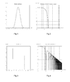
- Figure 2 illustrates the corresponding time frequency response of the diagram of figure 1 .
- Digital image capture devices have "electronic shutter", corresponding generally to the frame integration period of the CCD imager used as image sensing device.
- Figure 4 illustrates the corresponding time frequency response of the diagram of figure 3 , which is algebraically a cardinal sine function sinc( ⁇ ⁇ T ).
- This figure shows sidelobes effects with far higher magnitude compared to figure 2 .
- Such sidelobes effects with high magnitude may be very annoying, notably when they fall within the frequency sensibility range of human eye (i.e. below 50 Hz).
- apodization function By using a apodization function to apodize the response of the image sensing device during the exposure time or image sensing period of the capture of an image, the low pass filtering effect will still be improved and side lobe effects avoided or at least limited.
- Several apodization functions may be used to embody the invention. Unlike the rect(.) function (see above), these apodization functions go smoothly to zero at the beginning and the end of an integration of the captured light, thus preventing nonlinearity-related instabilities.
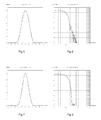
- Figure 5 illustrates the Hanning apodization function and the corresponding time frequency illustrated on figure 6 shows lower side lobes effects compared to figure 4 .
- FIG 7 illustrates the Blackman apodization function and the corresponding time frequency illustrated on figure 8 shows lower side lobes effects compared to figure 4 .
- Figure 9 illustrates the raised cosine apodization function and the corresponding time frequency illustrated on figure 10 shows again lower side lobes effects compared to figure 4 .
- AGC Automatic Gain Control
- said readout signal is proportional to the integral of intensity of illumination of a pixel over the duration of illumination of this pixel. Consequently, the combination of intensity and duration of illumination is represented by this integral.
- said driving means are also adapted to vary the number of successive illumination periods according to said predetermined image sensing period.
- the readout speed of the image sensing device may be a limitation for this number of successive illumination periods. In this situation, for very short image sensing periods, this number may be as low as four, and for longer image sensing periods, this number may be eight or higher.
- said apodization function is chosen in the group consisting of the Hanning apodization function, the Blackman apodization function, and the raised cosine apodization function.
- the subject of the invention is also a method to capture at least one image during an image sensing period comprising the followings steps :
- the driving means are adapted to capture images according to the following method.
- An important feature of the invention is notably adding at least an apodization step to the usual digital shutter process.
- the apodization function that is used is a Hanning function, which presents very little sidelobe effects (the gap over 30dB is between the main lobe and the first sidelobe). Any other apodization function or window can be used to implement the invention.
- Table 1 shows the values (and a rational approximation) of the approximation of the Hanning function for each illumination period, referenced 0 to 7, to be applied during shutter operation as a time-sequenced gain control.
- Each approximation of the Hanning function is then a weighting coefficient, also called an apodization coefficient.
- a new clock signal is defined and equals the shutter up signal uniformly divided by the number of apodization coefficients (8 in our case).
- the image buffer is empty.
- the readout signals provided by the image sensing device are read, then multiplied by the appropriate apodization coefficient, added to the current buffer values in the image buffer, and stored as new values in that same buffer.
- the image buffer is readout to obtain the captured image, and the image buffer is cleared for the next image or frame to capture.
- the above readout scheme is defined for a readout-with-discharge behavior of the imager, and therefore can apply to both CCD imagers and CMOS imagers.
- the readout signals provided by the image sensing device are read, subtracted to the values stored in Buffer1, multiplied by the appropriate apodization coefficient, then added to the current buffer2 values, and stored as new values in that same buffer.
- the pixel values provided by the image sensing device are also stored in Buffer1.
- the image buffer2 is readout to obtain the captured image, and the two image buffers are cleared for the next image or frame to capture.
Abstract
Description
- This invention applies to image capture devices, especially camcorder devices. A well-known issue in video capture is the apparition of visible flicker effects, for instance when filming with fluorescent lights or aiming at computer screens. When using a video capture device with a shutter, shutter synchronization can usually remove such artifacts. When using digital camcorders that generally do not comprise mechanical shutter, the abrupt temporal truncation of incoming photons in their light sensors made by electronic shutters may cause artifacts. This behavior is also responsible for increased motion blur artifacts.
- As technology improves, electronic control of camera shutters has been widely developed. Shutter control allows for instance to control the amount of motion that is recorded in a picture or video frame, by limiting exposure time prior to acquisition. Exposure time is determined by limiting the sampling time of the electronic sensor of the camera. As such control is completely electronic with no mechanical movement, this control can be very precise and reliable. However, from a digital signal processing theory point of view, because of their ultra-fast, "binary" (fully opened / fully closed) behavior, electronic shutters can present nonlinearity-related time-instability issues: the abrupt truncation of sensor illumination in time domain happens to generate a temporal ringing artifact known in signal processing theory as the "Gibbs" phenomenon.
- In space domain, the effects of such abrupt truncations are well known, as, for instance, the geometrical limits of a lens or of an optical filter. Well known spatial artifacts are, for instance, sidelobes of diffraction pattern. Such artifacts can be avoided, for instance, by using so-called "apodized" filters. Apodization literally means "removing the foot". It is the technical term for changing the shape of a mathematical function. It is also called tapering. In optical design jargon, an apodization function is used to purposely change the input intensity profile of an optical system. This technique is classically used in optics to remove the sidelobes of a diffraction pattern.
- The sharpness of an image capture device or of a component of an optical system (lens, film, image sensor, scanner, enlarging lens, etc.) is characterized by a parameter called Modulation Transfer Function (MTF), also known as spatial frequency response. It is well known to add apodized filters to get apodized lens aperture (or apodized stop), in order to improve the MTF of lenses : according to
US2007/139792 , "a perfectly apodized aperture is an aperture for which light transmission T varies along its radius x as a Gaussian curve". - An object of the invention is to avoid or at least limit the temporal ringing artifacts that are generally generated when using digital image capture devices.
- For this purpose, the subject of the invention is a device for capturing at least one image of an object field, comprising at least one image sensing device having an active surface made of an array of pixels and able to sense each of these pixels by providing a readout signal representative of the combination of intensity and duration of illumination of said pixel, an optical system able to form said image of an object field on said active surface such as to illuminate said active surface, and driving means able to drive said image sensing device and to assign a value to each pixel of said at least one image in order to capture it, wherein, an image sensing period of illumination of said active surface being predetermined for said capture, said driving means are adapted :
- to subdivide said image sensing period into a plurality of successive illumination periods,
- to assign to each pixel the sum of the readout signals provided by this pixel for each of said successive illumination periods, said sum being weighted by an apodization function.
- The image sensing period corresponds to the exposure time of an image to capture.
- The image sensing device may be for instance a CCD imager or a CMOS imager. Generally, each pixel of the imager is a light sensor.
- The readout signals provided by the image sensing device may an electric voltage or a digital signal. Electric voltages are generally converted into digital values before being summed and weighted.
- The optical system generally comprises an objective lens and may comprise prisms, notably when the image capture device comprises a plurality of image sensing device, generally one for each primary color, red, green and blue.
- Preferably, said driving means are adapted to capture sequences of images such as to get a video capture device. As a matter of fact, the advantages of the invention are notably obtained for video captures. Thank to the invention, temporal aliasing issues and temporal ringing artifacts are prevented or at least limited.
- In this invention, a new image sensor device matrix readout scheme with time-sequenced gain control is then proposed, thus providing a better truncation (or "apodization") operation of the electronic shutter. Such a readout scheme that is implemented by the driving means of the image capture device of the invention allows advantageously to simulate or emulate a mechanical shutter. As a matter of fact, as illustrated on
figure 1 , image capture devices having mechanical shutter have inherently an apodized shutter, because the shutter starts and stops (or opens and closes) progressively the flux of light.Figure 2 illustrates the corresponding time frequency response of the diagram offigure 1 . - Digital image capture devices have "electronic shutter", corresponding generally to the frame integration period of the CCD imager used as image sensing device. Such an electronic shutter opens and closes abruptly the flux of light, as illustrated by the rectangle function shown on
figure 3 and algebraically expressed as follows :
Figure 4 illustrates the corresponding time frequency response of the diagram offigure 3 , which is algebraically a cardinal sine function sinc(πƒT). This figure shows sidelobes effects with far higher magnitude compared tofigure 2 . Such sidelobes effects with high magnitude may be very annoying, notably when they fall within the frequency sensibility range of human eye (i.e. below 50 Hz). As it turns out, although electronic shutter operation's prime purpose is to prevent over/underexposure issues, i.e. too long or too short image sensing period, its time-integrating properties happen to make it behave as a pre-sampling lowpass filter, thus preventing temporal aliasing issues as well. Such a temporal filter's - 3dB cutoff frequency ƒc is directly related to the exposure time or image sensing period according to the following equations :
- Knowing that the sinc(.) function is polynomial (it has a rapidly convergent power series representation) and that a coarse approximation of the root of the above equations is fc = 1/2T, this equation can be numerically solved using the Newton-Raphson iterative method for finding roots:

- As an example, a shutter speed of T = 1/50 (corresponding to a standard configuration in PAL camcorders) generates a low pass filter with cutoff frequency at fc = 2.15Hz, thus preventing aliasing issues, since in this case harmonics over the

- By using a apodization function to apodize the response of the image sensing device during the exposure time or image sensing period of the capture of an image, the low pass filtering effect will still be improved and side lobe effects avoided or at least limited. Several apodization functions may be used to embody the invention. Unlike the rect(.) function (see above), these apodization functions go smoothly to zero at the beginning and the end of an integration of the captured light, thus preventing nonlinearity-related instabilities.
Figure 5 illustrates the Hanning apodization function and the corresponding time frequency illustrated onfigure 6 shows lower side lobes effects compared tofigure 4 .Figure 7 illustrates the Blackman apodization function and the corresponding time frequency illustrated onfigure 8 shows lower side lobes effects compared tofigure 4 .Figure 9 illustrates the raised cosine apodization function and the corresponding time frequency illustrated onfigure 10 shows again lower side lobes effects compared tofigure 4 . As we can see, because of the smooth truncation process "at the feet", such functions can limit sidelobe effects in the frequency domain. As sidelobes decrease, gain in the bandwidth tends to decrease as well, but this gain loss can be generally corrected using an Automatic Gain Control (AGC) that is usually embedded in a camcorder. - Preferably, said readout signal is proportional to the integral of intensity of illumination of a pixel over the duration of illumination of this pixel. Consequently, the combination of intensity and duration of illumination is represented by this integral.
- Preferably, said driving means are also adapted to vary the number of successive illumination periods according to said predetermined image sensing period. The readout speed of the image sensing device may be a limitation for this number of successive illumination periods. In this situation, for very short image sensing periods, this number may be as low as four, and for longer image sensing periods, this number may be eight or higher.
- Preferably, said apodization function is chosen in the group consisting of the Hanning apodization function, the Blackman apodization function, and the raised cosine apodization function.
- The subject of the invention is also a method to capture at least one image during an image sensing period comprising the followings steps :
- subdividing said image sensing period into a plurality of successive illumination periods;
- assigning to each pixel of said image a value proportional or equal to the sum of the integrals of intensity of illumination of this pixel over each of said successive illumination periods, wherein said sum is weighted by an apodization function.
- The invention will be more clearly understood on reading the description which follows, given by way of non-limiting example and with reference to the appended figures in which:
-
Figure 1 illustrates the time behavior of a mechanical shutter andfigure 2 illustrates the corresponding time frequency of this mechanical shutter ; -
Figure 3 illustrates the rectangle function representing the behavior of a usual electronic shutter andfigure 4 illustrates the corresponding time frequency of this function ; -
Figure 5 illustrates an Hanning apodization function used for the main embodiment of the invention andfigure 6 illustrates the corresponding time frequency of this function; -
Figure 7 illustrates a Blackman apodization function which may be used to implement the invention andfigure 8 illustrates the corresponding time frequency of this function; -
Figure 9 illustrates a Raised cosine apodization function which may be used to implement the invention andfigure 10 illustrates the corresponding time frequency of this function; -
Figure 11 illustrates the Hanning apodization function used for the main embodiment of the invention with the approximation of this function - apodization coefficient - for each illumination period as used in the main embodiment of the invention; -
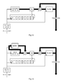
Figure 12 shows a first implementation of a readout scheme of the image sensing device that is used in the main embodiment of the invention; -
Figure 13 shows a second implementation of a readout scheme of the image sensing device that may be used as a variant of the main embodiment of the invention. - The present description illustrates the principles of the invention. It will thus be appreciated that those skilled in the art will be able to devise various arrangements that, although not explicitly described or shown herein, embody the same present principles and are included within its spirit and scope.
- The image capture device according to a main embodiment of the invention comprises :
- a CCD imager as a image sensing device ; this CCD imager has an active surface made of an array of pixels ; on operation and under illumination, this CCD imager senses each of these pixels by providing a readout signal proportional to the integral of intensity of illumination of this pixel over the duration of illumination of this pixel;
- an objective lens as part of an optical system able to form images of an object field on the active surface of the CCD imager, in order to illuminate the active surface of the CCD imager;
- and driving means able to drive the CCD imager in order to capture images formed on the active surface of this CCD imager by the optical system. These driving means comprises at least one image buffer to store pixel values provided by the CCD imager, a shift register to store apodization coefficients (see detail below), and a set of operators : sum, multiplication.
- The driving means are adapted to capture images according to the following method. An important feature of the invention is notably adding at least an apodization step to the usual digital shutter process. In this specific embodiment, the apodization function that is used is a Hanning function, which presents very little sidelobe effects (the gap over 30dB is between the main lobe and the first sidelobe). Any other apodization function or window can be used to implement the invention. The instrument function for Hanning apodization can be algebraically written as follows :

- The algebraical expression for an apodization-enabled shutter process of an incoming video signal x(t) of a given pixel will be expressed as follows :

- To implement
equation 2, we have to consider the fact that, for each pixel, a CCD imager (as a CMOS imager anyway) will only provide portions of the incoming illumination signals that are integrated over the duration of illumination of this pixel. This limitation comes from the usual readout electronics of these imagers. In the current embodiment of this invention, the exposure time of an image, i.e. the image sensing period, is split into eight equal portions, i.e. eight successive illumination periods. The number of successive illumination periods is generally limited by the imager readout speed and by the noise robustness possibilities. A weighting constant coefficient is extracted to approximate the Hanning function for each of these successive illumination periods, which leads to the following decomposition of the value assigned to each pixel by the driving means :
where, as illustrated onfigure 11 ,term 1 is the approximation of the Hanning function (
term 2 is the value provided by the CCD imager for this pixel, that is the integral of the illumination signal of this pixel over this given illumination period. Therefore, to each pixel, is assigned the sum of the readout signals (term 2) provided by this pixel for each of said successive illumination periods, this sum being weighted by the Hanning apodization function (term 1).Tableau 1 n 
(rational approximation) 0 0.0380602 1/32 1 0.3086583 10/32 2 0.6913417 22/32 3 0.9619398 31/32 4 0.9619398 31/32 5 0.6913417 22/32 6 0.3086583 10/32 7 0.0380602 1/32 - Table 1 shows the values (and a rational approximation) of the approximation of the Hanning function for each illumination period, referenced 0 to 7, to be applied during shutter operation as a time-sequenced gain control. Each approximation of the Hanning function is then a weighting coefficient, also called an apodization coefficient.
- In reference to
figure 12 , a first implementation of a readout scheme of the time-sequenced gain control according to table 1 will now be described. To implement this readout scheme, a new clock signal is defined and equals the shutter up signal uniformly divided by the number of apodization coefficients (8 in our case). Before starting to capture an image, the image buffer is empty. At each clock cycle, the readout signals provided by the image sensing device are read, then multiplied by the appropriate apodization coefficient, added to the current buffer values in the image buffer, and stored as new values in that same buffer. At the end of the last illumination period corresponding to the end of the image sensing period, the image buffer is readout to obtain the captured image, and the image buffer is cleared for the next image or frame to capture. - The above readout scheme is defined for a readout-with-discharge behavior of the imager, and therefore can apply to both CCD imagers and CMOS imagers.
- In reference to
figure 13 , a second implementation of a readout scheme of the time-sequenced gain control according to table 1 will now be described, which uses two image buffers Buffer1, Buffer2 instead of one. This readout scheme requires only one discharge per shutter cycle frame, thus improving noise robustness but limiting its usability to CMOS imagers only. To implement this readout scheme, a new clock signal is defined and equals the shutter up signal uniformly divided by the number of apodization coefficients (8 in our case). Before starting to capture an image, the image buffers Buffer1 and Buffer2 are empty. At each clock cycle, the readout signals provided by the image sensing device are read, subtracted to the values stored in Buffer1, multiplied by the appropriate apodization coefficient, then added to the current buffer2 values, and stored as new values in that same buffer. In the mean time the pixel values provided by the image sensing device are also stored in Buffer1. At the end of the last illumination period corresponding to the end of the image sensing period, the image buffer2 is readout to obtain the captured image, and the two image buffers are cleared for the next image or frame to capture. - Thank to these specific readout schemes using apodization coefficients, temporal aliasing issues and temporal ringing artifacts are prevented or at least limited in the captured images.
- These and other features and advantages of the present principles may be readily ascertained by one of ordinary skill in the pertinent art based on the teachings herein. It is to be understood that the teachings of the present principles may be implemented in various forms of hardware, software, firmware, special purpose processors, or combinations thereof.
- Although the illustrative embodiment above have been described herein with reference to the accompanying drawings, it is to be understood that the present principles are not limited to this precise embodiment, and that various changes and modifications may be effected therein by one of ordinary skill in the pertinent art without departing from the scope or spirit of the present principles. All such changes and modifications are intended to be included within the scope of the present principles as set forth in the appended claims.
Claims (7)
- Device for capturing at least one image of an object field, comprising at least one image sensing device having an active surface made of an array of pixels and able to sense each of these pixels by providing a readout signal representative of the combination of intensity and duration of illumination of said pixel, an optical system able to form said image of an object field on said active surface such as to illuminate said active surface, and driving means able to drive said image sensing device and to assign a value to each pixel of said at least one image in order to capture it,
characterized in that, an image sensing period of illumination of said active surface being predetermined for said capture, said driving means are adapted :- to subdivide said image sensing period into a plurality of successive illumination periods,- to assign to each pixel the sum of the readout signals provided by this pixel for each of said successive illumination periods, said sum being weighted by an apodization function. - Image capture device according to claim 1, characterized in that said driving means are adapted to capture sequences of images such as to get a video capture device.
- Image capture device according to claim 1 or 2 characterized in that said readout signal is proportional to the integral of intensity of illumination of a pixel over the duration of illumination of this pixel.
- Image capture device according any one of claims 1 to 3 characterized in that said driving means are also adapted to vary the number of successive illumination periods according to said predetermined image sensing period.
- Image capture device according to any one of the preceding claims characterized in that said apodization function is chosen in the group consisting of the Hanning apodization function, the Blackman apodization function, and the raised cosine apodization function.
- Method to capture at least one image during an image sensing period comprising the followings steps :- subdividing said image sensing period into a plurality of successive illumination periods;- assigning to each pixel of said image a value proportional or equal to the sum of the integrals of intensity of illumination of this pixel over each of said successive illumination periods, wherein said sum is weighted by an apodization function.
- Method according to claim 6, characterized in that said apodization function is chosen in the group consisting of the Hanning apodization function, the Blackman apodization function, and the raised cosine apodization function.
Priority Applications (6)
| Application Number | Priority Date | Filing Date | Title |
|---|---|---|---|
| EP08305992A EP2200277A1 (en) | 2008-12-22 | 2008-12-22 | Method and device to capture images by emulating a mechanical shutter |
| JP2011542802A JP5491523B2 (en) | 2008-12-22 | 2009-12-21 | Method and device for capturing images by emulating a mechanical shutter |
| US12/998,982 US9237276B2 (en) | 2008-12-22 | 2009-12-21 | Method and device to capture images by emulating a mechanical shutter |
| KR1020117014321A KR101620520B1 (en) | 2008-12-22 | 2009-12-21 | Method and device to capture images by emulating a mechanical shutter |
| PCT/EP2009/067651 WO2010072718A1 (en) | 2008-12-22 | 2009-12-21 | Method and device to capture images by emulating a mechanical shutter |
| EP09795777A EP2368361A1 (en) | 2008-12-22 | 2009-12-21 | Method and device to capture images by emulating a mechanical shutter |
Applications Claiming Priority (1)
| Application Number | Priority Date | Filing Date | Title |
|---|---|---|---|
| EP08305992A EP2200277A1 (en) | 2008-12-22 | 2008-12-22 | Method and device to capture images by emulating a mechanical shutter |
Publications (1)
| Publication Number | Publication Date |
|---|---|
| EP2200277A1 true EP2200277A1 (en) | 2010-06-23 |
Family
ID=40344256
Family Applications (2)
| Application Number | Title | Priority Date | Filing Date |
|---|---|---|---|
| EP08305992A Withdrawn EP2200277A1 (en) | 2008-12-22 | 2008-12-22 | Method and device to capture images by emulating a mechanical shutter |
| EP09795777A Withdrawn EP2368361A1 (en) | 2008-12-22 | 2009-12-21 | Method and device to capture images by emulating a mechanical shutter |
Family Applications After (1)
| Application Number | Title | Priority Date | Filing Date |
|---|---|---|---|
| EP09795777A Withdrawn EP2368361A1 (en) | 2008-12-22 | 2009-12-21 | Method and device to capture images by emulating a mechanical shutter |
Country Status (5)
| Country | Link |
|---|---|
| US (1) | US9237276B2 (en) |
| EP (2) | EP2200277A1 (en) |
| JP (1) | JP5491523B2 (en) |
| KR (1) | KR101620520B1 (en) |
| WO (1) | WO2010072718A1 (en) |
Cited By (2)
| Publication number | Priority date | Publication date | Assignee | Title |
|---|---|---|---|---|
| US9686474B2 (en) | 2010-09-09 | 2017-06-20 | Red.Com, Inc. | Optical filter opacity control for reducing temporal aliasing in motion picture capture |
| US9854180B2 (en) | 2013-04-05 | 2017-12-26 | Red.Com, Llc | Optical filtering for electronic devices |
Families Citing this family (5)
| Publication number | Priority date | Publication date | Assignee | Title |
|---|---|---|---|---|
| FR2968878A1 (en) * | 2010-12-14 | 2012-06-15 | Thomson Licensing | METHOD AND DEVICE FOR GENERATING IMAGES COMPRISING KINETIC FLOU |
| WO2013088442A1 (en) * | 2011-12-15 | 2013-06-20 | Pebbles Ltd. | Controllable optical sensing |
| NL2018853B1 (en) * | 2017-05-05 | 2018-11-14 | Illumina Inc | Systems and methods for improved focus tracking using a hybrid mode light source |
| CN109754448B (en) * | 2018-12-29 | 2023-01-17 | 深圳安科高技术股份有限公司 | CT cardiac scanning artifact correction method and system |
| CN111263082B (en) * | 2020-03-16 | 2021-12-14 | 维沃移动通信(杭州)有限公司 | Exposure data acquisition method and electronic equipment |
Citations (3)
| Publication number | Priority date | Publication date | Assignee | Title |
|---|---|---|---|---|
| WO2006088722A2 (en) * | 2005-02-14 | 2006-08-24 | Canesta, Inc. | Method and system to increase dynamic range of time-of-flight (tof) and/or imaging sensors |
| WO2006094871A1 (en) * | 2005-03-08 | 2006-09-14 | Sony Ericsson Mobile Communications Ab | Method and device for creating pictures |
| US20070139792A1 (en) | 2005-12-21 | 2007-06-21 | Michel Sayag | Adjustable apodized lens aperture |
Family Cites Families (31)
| Publication number | Priority date | Publication date | Assignee | Title |
|---|---|---|---|---|
| JPS63105580A (en) | 1986-10-22 | 1988-05-10 | Hitachi Ltd | Television camera |
| US4910693A (en) | 1987-12-29 | 1990-03-20 | Hughes Aircraft Company | Method and apparatus for sampling lattice pattern generation and processing |
| JPH02252371A (en) | 1989-03-24 | 1990-10-11 | Fujitsu General Ltd | Auto-flickerless circuit for ccd camera |
| RU1779931C (en) | 1990-06-29 | 1992-12-07 | Институт космических исследований АН СССР | Solar sensor |
| GB2247587B (en) | 1990-08-31 | 1994-07-20 | Sony Broadcast & Communication | Movie film and video production |
| JP2554955B2 (en) | 1990-10-02 | 1996-11-20 | 池上通信機株式会社 | Non-linear processing circuit |
| US5606366A (en) * | 1991-10-28 | 1997-02-25 | Canon Kabushiki Kaisha | Image sensor driving apparatus wherein photoelectric conversion operations are performed a plurality of times |
| JP2995887B2 (en) | 1991-03-27 | 1999-12-27 | 松下電器産業株式会社 | Flicker correction circuit |
| JPH0888794A (en) | 1994-09-20 | 1996-04-02 | Fujitsu General Ltd | Flickerless ccd camera |
| TW405301B (en) | 1997-08-07 | 2000-09-11 | Koninkl Philips Electronics Nv | A method for converting an analog input signal into a digital output signal, an arrangement for performing such method and an image sensor comprising such arrangements |
| EP0912047B1 (en) | 1997-10-23 | 2004-04-07 | Olympus Optical Co., Ltd. | Imaging apparatus comprising means for expanding the dynamic range |
| US6100937A (en) * | 1998-05-29 | 2000-08-08 | Conexant Systems, Inc. | Method and system for combining multiple images into a single higher-quality image |
| JP2001024941A (en) * | 1999-07-06 | 2001-01-26 | Victor Co Of Japan Ltd | Electronic camera |
| US6778210B1 (en) * | 1999-07-15 | 2004-08-17 | Olympus Optical Co., Ltd. | Image pickup apparatus with blur compensation |
| US6442203B1 (en) * | 1999-11-05 | 2002-08-27 | Demografx | System and method for motion compensation and frame rate conversion |
| EP1176807A1 (en) | 2000-07-24 | 2002-01-30 | Agilent Technologies, Inc. (a Delaware corporation) | Skewed pixel pattern sub-sampling for image sensor |
| US7298401B2 (en) * | 2001-08-10 | 2007-11-20 | Micron Technology, Inc. | Method and apparatus for removing flicker from images |
| JP2004112739A (en) | 2002-07-25 | 2004-04-08 | Fujitsu Ltd | Solid-state image sensor |
| US7142234B2 (en) | 2002-12-10 | 2006-11-28 | Micron Technology, Inc. | Method for mismatch detection between the frequency of illumination source and the duration of optical integration time for imager with rolling shutter |
| JP4269850B2 (en) * | 2003-09-02 | 2009-05-27 | ソニー株式会社 | Imaging device |
| EP1544792A1 (en) | 2003-12-18 | 2005-06-22 | Thomson Licensing S.A. | Device and method for creating a saliency map of an image |
| JP4367264B2 (en) | 2004-07-12 | 2009-11-18 | セイコーエプソン株式会社 | Image processing apparatus, image processing method, and image processing program |
| US20060158399A1 (en) | 2005-01-14 | 2006-07-20 | Semiconductor Energy Laboratory Co., Ltd. | Driving method of display device |
| KR100674957B1 (en) | 2005-02-23 | 2007-01-26 | 삼성전자주식회사 | Solid state image sensing device and driving method for averaging and sub-sampling analog signals at an arbitrary sub-sampling rate |
| KR100660869B1 (en) | 2005-07-06 | 2006-12-26 | 삼성전자주식회사 | Image sensor and method for subsampling of enhanced frame rate and display quality |
| EP1764736A1 (en) | 2005-09-19 | 2007-03-21 | Thomson Licensing | Method and device for image cropping |
| EP1814073A1 (en) | 2006-01-26 | 2007-08-01 | THOMSON Licensing | Method and device for processing a sequence of video images |
| IL176694A0 (en) * | 2006-07-04 | 2006-10-31 | Univ Ramot | Method and device for low light level imaging |
| WO2008031089A2 (en) * | 2006-09-08 | 2008-03-13 | Sarnoff Corporation | System and method for high performance image processing |
| JP4843461B2 (en) | 2006-11-13 | 2011-12-21 | 株式会社東芝 | Solid-state imaging device |
| US20080143840A1 (en) * | 2006-12-19 | 2008-06-19 | Texas Instruments Incorporated | Image Stabilization System and Method for a Digital Camera |
-
2008
- 2008-12-22 EP EP08305992A patent/EP2200277A1/en not_active Withdrawn
-
2009
- 2009-12-21 KR KR1020117014321A patent/KR101620520B1/en not_active IP Right Cessation
- 2009-12-21 US US12/998,982 patent/US9237276B2/en not_active Expired - Fee Related
- 2009-12-21 EP EP09795777A patent/EP2368361A1/en not_active Withdrawn
- 2009-12-21 JP JP2011542802A patent/JP5491523B2/en not_active Expired - Fee Related
- 2009-12-21 WO PCT/EP2009/067651 patent/WO2010072718A1/en active Application Filing
Patent Citations (3)
| Publication number | Priority date | Publication date | Assignee | Title |
|---|---|---|---|---|
| WO2006088722A2 (en) * | 2005-02-14 | 2006-08-24 | Canesta, Inc. | Method and system to increase dynamic range of time-of-flight (tof) and/or imaging sensors |
| WO2006094871A1 (en) * | 2005-03-08 | 2006-09-14 | Sony Ericsson Mobile Communications Ab | Method and device for creating pictures |
| US20070139792A1 (en) | 2005-12-21 | 2007-06-21 | Michel Sayag | Adjustable apodized lens aperture |
Non-Patent Citations (1)
| Title |
|---|
| WIKIPEDIA: "Multiple exposure", INTERNET CITATION, 29 September 2008 (2008-09-29), XP007907272, Retrieved from the Internet <URL:http://en.wikipedia.org/wiki/Multiple_exposure> [retrieved on 20090217] * |
Cited By (6)
| Publication number | Priority date | Publication date | Assignee | Title |
|---|---|---|---|---|
| US9686474B2 (en) | 2010-09-09 | 2017-06-20 | Red.Com, Inc. | Optical filter opacity control for reducing temporal aliasing in motion picture capture |
| US10129484B2 (en) | 2010-09-09 | 2018-11-13 | Red.Com Llc | Optical filter opacity control for reducing temporal aliasing in motion picture capture |
| EP2628046B1 (en) * | 2010-09-09 | 2019-05-01 | Red.Com, Llc | Apparatus and method for reducing or preventing temporal aliasing in motion picture cameras |
| US10630908B2 (en) | 2010-09-09 | 2020-04-21 | Red.Com, Llc | Optical filter opacity control in motion picture capture |
| US9854180B2 (en) | 2013-04-05 | 2017-12-26 | Red.Com, Llc | Optical filtering for electronic devices |
| US10187588B2 (en) | 2013-04-05 | 2019-01-22 | Red.Com, Llc | Optical filtering for electronic devices |
Also Published As
| Publication number | Publication date |
|---|---|
| JP5491523B2 (en) | 2014-05-14 |
| KR101620520B1 (en) | 2016-05-12 |
| WO2010072718A1 (en) | 2010-07-01 |
| US9237276B2 (en) | 2016-01-12 |
| EP2368361A1 (en) | 2011-09-28 |
| KR20110103967A (en) | 2011-09-21 |
| JP2012513716A (en) | 2012-06-14 |
| US20110254998A1 (en) | 2011-10-20 |
Similar Documents
| Publication | Publication Date | Title |
|---|---|---|
| EP2200277A1 (en) | Method and device to capture images by emulating a mechanical shutter | |
| TWI496463B (en) | Method of forming full-color image | |
| JP5493010B2 (en) | Imaging apparatus and focus position detection method thereof | |
| JP4186699B2 (en) | Imaging apparatus and image processing apparatus | |
| EP1753226A1 (en) | Imaging device and signal processing method | |
| KR101374971B1 (en) | Reduced position dependent noise in digital images | |
| JP5527781B2 (en) | How to improve image quality | |
| JP5169318B2 (en) | Imaging apparatus and imaging method | |
| EP2008446A2 (en) | Adjustable neutral density filter system for dynamic range compression from scene to imaging sensor | |
| JP2010239492A (en) | Image pickup apparatus, and noise reduction method for video signal | |
| KR20080095084A (en) | Method and apparatus for reducing noise of image | |
| JP2004222231A (en) | Image processing apparatus and image processing program | |
| US11089202B2 (en) | Focus adjustment for image capture device | |
| JP2015103971A (en) | Solid-state imaging device and digital camera | |
| WO2012015628A2 (en) | Method for reducing image artifacts produced by a cmos camera | |
| KR100934730B1 (en) | Adaptive noise reduction device and image sensor using the device | |
| US11533423B2 (en) | Contrast-based autofocus | |
| JP3767188B2 (en) | Electronic camera and signal correction method | |
| JP2004222233A (en) | Image processing apparatus and image processing program | |
| JP2006180270A (en) | Image processor, imaging device, image processing method, program, and recording medium | |
| JP2011135379A (en) | Imaging apparatus, imaging method and program | |
| EP2632146B1 (en) | Image processing apparatus | |
| JP4487477B2 (en) | Noise suppression device | |
| JP2010268295A (en) | Photographing device and image processing method | |
| CN115955609A (en) | Method and system for stray light compensation |
Legal Events
| Date | Code | Title | Description |
|---|---|---|---|
| PUAI | Public reference made under article 153(3) epc to a published international application that has entered the european phase |
Free format text: ORIGINAL CODE: 0009012 |
|
| AK | Designated contracting states |
Kind code of ref document: A1 Designated state(s): AT BE BG CH CY CZ DE DK EE ES FI FR GB GR HR HU IE IS IT LI LT LU LV MC MT NL NO PL PT RO SE SI SK TR |
|
| AX | Request for extension of the european patent |
Extension state: AL BA MK RS |
|
| AKY | No designation fees paid | ||
| REG | Reference to a national code |
Ref country code: DE Ref legal event code: R108 Effective date: 20110201 Ref country code: DE Ref legal event code: 8566 |
|
| STAA | Information on the status of an ep patent application or granted ep patent |
Free format text: STATUS: THE APPLICATION IS DEEMED TO BE WITHDRAWN |
|
| 18D | Application deemed to be withdrawn |
Effective date: 20101224 |