EP2197043A1 - Solar battery manufacturing method - Google Patents
Solar battery manufacturing method Download PDFInfo
- Publication number
- EP2197043A1 EP2197043A1 EP08832433A EP08832433A EP2197043A1 EP 2197043 A1 EP2197043 A1 EP 2197043A1 EP 08832433 A EP08832433 A EP 08832433A EP 08832433 A EP08832433 A EP 08832433A EP 2197043 A1 EP2197043 A1 EP 2197043A1
- Authority
- EP
- European Patent Office
- Prior art keywords
- buffer layer
- target
- intermediate electrode
- solar cell
- sputtering
- Prior art date
- Legal status (The legal status is an assumption and is not a legal conclusion. Google has not performed a legal analysis and makes no representation as to the accuracy of the status listed.)
- Withdrawn
Links
Images




Classifications
-
- H—ELECTRICITY
- H10—SEMICONDUCTOR DEVICES; ELECTRIC SOLID-STATE DEVICES NOT OTHERWISE PROVIDED FOR
- H10F—INORGANIC SEMICONDUCTOR DEVICES SENSITIVE TO INFRARED RADIATION, LIGHT, ELECTROMAGNETIC RADIATION OF SHORTER WAVELENGTH OR CORPUSCULAR RADIATION
- H10F71/00—Manufacture or treatment of devices covered by this subclass
- H10F71/138—Manufacture of transparent electrodes, e.g. transparent conductive oxides [TCO] or indium tin oxide [ITO] electrodes
-
- C—CHEMISTRY; METALLURGY
- C23—COATING METALLIC MATERIAL; COATING MATERIAL WITH METALLIC MATERIAL; CHEMICAL SURFACE TREATMENT; DIFFUSION TREATMENT OF METALLIC MATERIAL; COATING BY VACUUM EVAPORATION, BY SPUTTERING, BY ION IMPLANTATION OR BY CHEMICAL VAPOUR DEPOSITION, IN GENERAL; INHIBITING CORROSION OF METALLIC MATERIAL OR INCRUSTATION IN GENERAL
- C23C—COATING METALLIC MATERIAL; COATING MATERIAL WITH METALLIC MATERIAL; SURFACE TREATMENT OF METALLIC MATERIAL BY DIFFUSION INTO THE SURFACE, BY CHEMICAL CONVERSION OR SUBSTITUTION; COATING BY VACUUM EVAPORATION, BY SPUTTERING, BY ION IMPLANTATION OR BY CHEMICAL VAPOUR DEPOSITION, IN GENERAL
- C23C14/00—Coating by vacuum evaporation, by sputtering or by ion implantation of the coating forming material
- C23C14/06—Coating by vacuum evaporation, by sputtering or by ion implantation of the coating forming material characterised by the coating material
- C23C14/08—Oxides
- C23C14/086—Oxides of zinc, germanium, cadmium, indium, tin, thallium or bismuth
-
- H—ELECTRICITY
- H10—SEMICONDUCTOR DEVICES; ELECTRIC SOLID-STATE DEVICES NOT OTHERWISE PROVIDED FOR
- H10F—INORGANIC SEMICONDUCTOR DEVICES SENSITIVE TO INFRARED RADIATION, LIGHT, ELECTROMAGNETIC RADIATION OF SHORTER WAVELENGTH OR CORPUSCULAR RADIATION
- H10F77/00—Constructional details of devices covered by this subclass
- H10F77/20—Electrodes
- H10F77/244—Electrodes made of transparent conductive layers, e.g. transparent conductive oxide [TCO] layers
-
- Y—GENERAL TAGGING OF NEW TECHNOLOGICAL DEVELOPMENTS; GENERAL TAGGING OF CROSS-SECTIONAL TECHNOLOGIES SPANNING OVER SEVERAL SECTIONS OF THE IPC; TECHNICAL SUBJECTS COVERED BY FORMER USPC CROSS-REFERENCE ART COLLECTIONS [XRACs] AND DIGESTS
- Y02—TECHNOLOGIES OR APPLICATIONS FOR MITIGATION OR ADAPTATION AGAINST CLIMATE CHANGE
- Y02E—REDUCTION OF GREENHOUSE GAS [GHG] EMISSIONS, RELATED TO ENERGY GENERATION, TRANSMISSION OR DISTRIBUTION
- Y02E10/00—Energy generation through renewable energy sources
- Y02E10/50—Photovoltaic [PV] energy
Definitions
- the present invention relates to a method for manufacturing a solar cell.
- Priority is claimed on Japanese Patent Application No. 2007-242609, filed September 19, 2007 , the contents of which are incorporated herein by reference.
- ITO In 2 O 3 -SnO 2
- a transparent conductive material has been used to form the electrodes of solar cells.
- ITO indium
- a ZnO-based material has been recognized for its availability and low price (see, for example, Patent Document 1).
- the ZnO-based material is suited for sputtering to deposit a uniform film on a large-sized substrate. A film may be deposited in a simple manner by substituting a target of the ZnO-based material for an In 2 O 3 -based material.
- the ZnO-based material does not include lower oxide (InO) having high insulating property which the In 2 O 3 -based material possesses.
- an existing solar cell includes: a glass substrate 51 constituting a surface of the solar cell; an upper electrode 53 provided on the glass substrate 51; a top cell 55 formed of amorphous silicon; an intermediate electrode 57 being a transparent conductive film and disposed between the top cell 55 and the bottom cell 59, which will be described later; a bottom cell 59 formed of microcrystal silicon; a buffer layer 61 being a transparent conductive film; and a rear electrode 63 being a metal film, which constituents are laminated together. It has been proposed to employ a ZnO-based film as the intermediate electrode 57 or the buffer layer 61 of the thus-configured solar cell.
- the intermediate electrode 57 is formed through magnetron sputtering, there is a possibility that plasma-excited negative ions are accelerated and bombarded onto the substrate, and this bombardment may cause damage to the underlying top cell 55. Similarly, in the process of forming the buffer layer 61, the underlying bottom cell 59 may be damaged.
- the intermediate electrode 57 is highly light transmissive so that light passing through the top cell 55 can enter the bottom cell 59 to generate electricity.
- the buffer layer 61 is highly light transmissive so that light passing through the bottom cell 59 is reflected at the rear electrode 63 and re-enter the bottom cell 59 to generate electricity.
- the invention is made in view of the aforementioned circumstances and an object thereof is to provide a method for manufacturing a solar cell including a transparent conductive film of a highly light transmissive ZnO-based material, the method can reduce damage to underlying layers.
- the invention employs the followings in order to solve the aforementioned problems and achieve the object.
- low sputtering voltage can be employed to form the intermediate electrode or the buffer layer and, therefore, acceleration of plasma-excited negative ions and bombardment of the negative ions onto the substrate can be suppressed. Accordingly, in the manufacturing process of the solar cell, damage to underlying films of a photovoltaic cell and the like disposed adjacent to the intermediate electrode or the buffer layer, can be reduced.
- the sputtering voltage of 340V or less, a thin ZnO-based film with a well-defined crystalline lattice can be deposited, therefore a transparent conductive film with low specific resistance can be provided.
- the target may preferably be sputtered while introducing oxygen gas or oxygen atom-containing gas.
- oxygen gas or oxygen atom-containing gas introducing oxygen gas or oxygen atom-containing gas.
- an oxygen-rich ZnO-based film is provided and, therefore, a highly light transmissive transparent conductive film can be obtained.
- a magnetic field generating device for generating a horizontal magnetic field on the target surface may preferably include a first magnet with a first polarity and a second magnet with a second polarity disposed along a rear surface of the target; and the second magnet is disposed to surround the first magnet.
- a strong horizontal magnetic field can be generated on the target surface to facilitate formation of a ZnO-based film with a well-defined crystalline lattice.
- a transparent conductive film with a low specific resistance and a high heat resistance can be provided.
- the target may preferably be sputtered while relative positions of the magnetic field generating device for generating a horizontal magnetic field on the target surface and the target are changing. In this case, a non-eroded area can be reduced. In addition, efficiency in the use of the target can be increased and introduced power can be increased.
- the target may preferably be sputtered while relative positions of a substrate on which the intermediate electrode or the buffer layer is to be formed and the target are changing.
- a uniform transparent conductive film can be provided on the entire substrate.
- the sputtering voltage may preferably be applied from both a direct current power supply and a high-frequency power supply.
- low sputtering voltage can be employed. With such the low sputtering voltage, acceleration of the plasma-excited negative ions and bombardment of the negative ions to the substrate can be suppressed. Accordingly, in the manufacturing process of the solar cell, damage to underlying films of a photovoltaic cell and the like disposed adjacent to the intermediate electrode or the buffer layer, can be reduced.
- low sputtering voltage can be employed to form the intermediate electrode or the buffer layer and, therefore, acceleration of plasma-excited negative ions and bombardment of the negative ions to the substrate can be suppressed.
- a solar cell that includes a transparent conductive film of a highly light transmissive ZnO-based material can be provided.
- FIG. 1 schematically illustrates a configuration of a magnetron sputtering apparatus.
- a sputtering apparatus 10 is an interback-type sputtering apparatus, which includes a carry-in/out chamber 12 for a substrate (not shown in FIG.1 ) and a film deposition chamber 14 in which a film is deposited on the substrate.
- a roughing exhauster 12p such as a rotary pump, is connected to the carry-in/out chamber 12.
- a high-vacuum exhauster 14p such as a turbo-molecular pump, is connected to the film deposition chamber 14.
- the substrate supported in a vertical position is carried into the carry-in/out chamber 12, and then the carry-in/out chamber 12 is evacuated by the roughing exhauster 12p.
- the substrate is conveyed into the film deposition chamber 14 which is highly evacuated by a high-vacuum exhauster 14p, and then a film is deposited on the substrate.
- the substrate having a film deposited thereon is taken out via the carry-in/out chamber 12.
- a gas supply unit 17 which supplies sputtering gas, such as Ar, is connected to the film deposition chamber 14.
- the gas supply unit 17 may also supply reactant gas, such as O 2 .
- a sputtering cathode mechanism 20 is disposed vertically in the film deposition chamber 14.
- FIG. 2 is a plan view of the film deposition chamber 14.
- the sputtering cathode mechanism 20 is disposed at one width-direction end of the film deposition chamber 14.
- a heater 18 for heating the substrate 5 is disposed at another width-direction end of the film deposition chamber 14.
- the sputtering cathode mechanism 20 mainly includes a target 22, a backing plate 24 and a magnetic circuit 30.
- the backing plate 24 is connected to a DC power supply 26 and held at negative potential.
- a target 22 brazed with a formation material of the ZnO-based film is disposed on a surface of the backing plate 24.
- the formation material of the ZnO-based film is ZnO to which an Al-containing material is doped.
- Sputtering gas is supplied into the film deposition chamber 14 from the gas supply unit 17, and sputtering voltage is applied to the backing plate 24 by the DC power supply 26.
- sputtering gas ions excited by plasma within the film deposition chamber 14 bombard the target 22 so that atoms of the formation material of the ZnO-based film are ejected.
- the ejected atoms adhere to the substrate 5 to provide a film of the ZnO-based material on the substrate 5.
- a magnetic circuit 30 generating a horizontal magnetic field on a surface of the target 22 is placed along a back surface of the backing plate 24.
- the magnetic circuit 30 includes a first magnet 31 and a second magnet 32 which are polarized opposite to each other at their surfaces facing the backing plate 24.
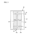
- FIG. 3 is a rear elevation of the sputtering cathode mechanism 20.
- the first magnet 31 is disposed linearly.
- the second magnet 32 is disposed in a frame configuration surrounding the first magnet 31 with a predetermined distance from a periphery of the first magnet 31.
- the first magnets 31 and the second magnets 32 are mounted on a yoke 34 to form a magnetic circuit unit 30a.
- Multiple (two in the present embodiment) magnetic circuit units 30a and 30b are connected to each other with a bracket 35 to form the magnetic circuit 30.
- a magnetic field represented by a magnetic field line 36 is generated by the first magnet 31 and the second magnet 32 which are polarized opposite to each other at the backing plate 24 side thereof.
- positions 37 with a vertical magnetic field of 0 (and the maximum horizontal magnetic field) appear on the surface of the target 22 between the first magnet 31 and the second magnet 32.
- the film deposition speed is accelerated.
- the target 22 is eroded most deeply at the positions 37.
- the magnetic circuit 30 may fluctuate horizontally so that the positions 37 are not fixed in order to increase the efficiency in the use of the target (i.e., lifetime of the target) and that cooling efficiency of the target and the cathode is increased in order to improve arcing or other property.
- the eroded configuration is rectangular or semicircular at upper and lower ends of the target 22.
- the magnetic circuit 30 may also fluctuate vertically.
- a pair of horizontal and vertical actuators (not illustrated) are provided to make the bracket 35 of the magnetic circuit 30 reciprocate horizontally and vertically. When these horizontal and vertical actuators are driven at different cycles, the magnetic circuit 30 fluctuates in a zigzag manner within a surface parallel to the target 22.
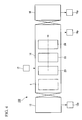
- FIG. 4 illustrates a modified embodiment of the magnetron sputtering apparatus.
- a sputtering apparatus 100 is an in-line type sputtering apparatus which includes a carry-in chamber 12, a film deposition chamber 14 and a carry-out chamber 16 in this order.
- the substrate supported in a vertical position is carried into the carry-in chamber 12 and then the carry-in chamber 12 is evacuated by a roughing exhauster 12p.
- the substrate 5 is conveyed into the film deposition chamber 14 which is highly evacuated by a high-vacuum exhauster 14p where a film is deposited on the substrate 5.
- the substrate 5 having a film deposited thereon is taken out via the carry-out chamber 16 which is evacuated by a roughing exhauster 16p.
- sputtering cathode mechanisms 20 are disposed in a conveyance direction of the substrate 5 within the film deposition chamber 14. Each sputtering cathode mechanism 20 is configured in the same manner as that of the embodiment described above. In the modified embodiment, a ZnO-based film is formed on a surface of the substrate 5 with the each sputtering cathode mechanisms 20 as the substrate 5 passes in front of the sputtering cathode mechanisms 20. In this manner, a uniform ZnO-based film can be deposited with increased throughput of the film deposition process.
- FIG. 5 schematically illustrates a configuration of the solar cell.
- the solar cell 50 includes: a glass substrate 51 constituting a surface of the solar cell 50; an upper electrode 53 comprising a transparent conductive film and provided on the glass substrate 51; a top cell 55 formed of amorphous silicon; an intermediate electrode 57 being a transparent conductive film and disposed between the top cell 55 and the bottom cell 59, which will be described later; a bottom cell 59 formed of microcrystal silicon; a buffer layer 61 being a transparent conductive film; and a rear electrode 63 being a metal film; which are laminated together.
- the solar cell 50 is an a-Si/micro crystallite Si tandem solar cell.
- short wavelength light is absorbed by the top cell 55 and long wavelength light is absorbed by the bottom cell 59.
- power generation efficiency can be increased.
- the top cell 55 has a three layer structure consisting of a p-layer (55p), an i-layer (55i) and an n-layer (55n).
- the i-layer (55i) is formed of amorphous silicon.
- the bottom cell 59 also has a three-layer structure consisting of a p-layer (59p), an i-layer (59i) and an n-layer (59n) like the top cell 55.
- the i-layer (59i) is formed of microcrystal silicon.
- the solar cell 50 employs a texture structure which provides a prism effect for extending an optical path of sunlight incident into the upper electrode 53 and a light trapping effect.
- the intermediate electrode 57 and the buffer layer 61 of the solar cell 50 according to the present embodiment are configured by a ZnO-based film (i.e., a transparent conductive film) formed with the magnetron sputtering apparatus 10 described above. If the intermediate electrode 57 is formed through magnetron sputtering, there is a possibility that plasma-excited negative ions are accelerated and bombarded onto the substrate, and this bombardment may cause damage to the underlying top cell 55. Similarly, in the process of forming the buffer layer 61, the underlying bottom cell 59 may be damaged. It is therefore necessary that the intermediate electrode 57 or the buffer layer 59 is formed while suppressing damage to the underlying layers.
- the buffer layer 61 is provided also in order to prevent diffusion of the metal layer used as the rear electrode 63.
- a solar cell 50 is manufactured with a sputtering device 10 illustrated in FIGS. 1 to 3 .
- the upper electrode 53 is formed on the glass substrate 51 in the same manner as that of the intermediate electrode 57, which will be described later.
- the top cell 55 is then formed on the upper electrode 53.
- an Al-added ZnO (AZO) film is formed on the top cell 55 as the intermediate electrode 57.
- AZO Al-added ZnO
- a method for forming the intermediate electrode 57 through magnetron sputtering will be described below.
- a ZnO material to which Al 2 O 3 is doped in an amount of 0.5 to 10.0 wt% (2.0 wt% in the present embodiment) is employed to form the transparent conductive film.
- a non-alkali glass substrate 51 is carried into the film deposition chamber 14 and heated as needed with the heater 18. When the glass substrate 51 is heated with the heater 18, temperature of the heated glass substrate 51 may preferably be 200°C or less.
- the film deposition chamber 14 is highly evacuated by the high-vacuum exhauster 14p. Ar gas is introduced into the film deposition chamber 14 as a sputtering gas from the gas supply unit 17. Pressure in the film deposition chamber 14 is kept at 2 to 10 mTorr (5 mTorr in the present embodiment).
- Electric power having power density of 1 to 8 W/cm 2 (4 W/cm 2 in the present embodiment) is introduced to the backing plate 24 from the DC power supply 26 while the magnetic circuit 30 is fluctuating.
- the thus-deposited film is not annealed because the film is deposited with heat, the deposited film may be annealed alternatively.
- the conductivity of the ZnO-based film increases when Al or other substances enter Zn sites in the crystals, form ions and emit free electrons.
- An Al 2 O 3 -doped ZnO target is sputtered to form an Al- doped ZnO (AZO) film to obtain a transparent conductive film with low specific resistance. In this manner, a transparent conductive film with especially low specific resistance among other ZnO-based films can be obtained.
- the present inventors evaluated dependency of specific resistance of the ZnO-based film to magnetic field strength.
- the ZnO-based film was formed at two levels: a first level in which the magnetic circuit 30 was controlled to have a 300-gauss horizontal magnetic field strength on the target surface; and a second level in which the magnetic circuit 30 was controlled to have 1500-gauss horizontal magnetic field strength on the target surface.
- Specific resistance of the obtained ZnO-based films of each level having a thickness of 2000, 5000, 10000 and 15000 angstroms was measured.
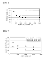
- FIG. 6 is a graph illustrating a relationship between horizontal magnetic field strength and sputtering voltage.
- the sputtering voltage decreases as illustrated in FIG. 6 .
- sputtering voltage is affected by discharge impedance (i.e., target voltage/target current) and the discharge impedance is affected by magnetic field strength on the target surface.
- plasma density As magnetic field strength becomes large, plasma density also becomes large and, as a result, sputtering voltage decreases.
- Sputtering voltage of the first level horizontal magnetic field strength: 300 gauss
- sputtering voltage of the second level is about 300V
- FIG. 7 is a graph illustrating a relationship between the thickness of the ZnO-based film and specific resistance. Since specific resistance of the ZnO-based material depends on the film thickness, the specific resistance decreases as the thickness increases. The specific resistance of the ZnO-based film formed at the second level (1500 gauss, 300V) is smaller than that of the first level (300 gauss, 435V). The reason for this phenomenon is considered as follows. Since the specific resistance depends on the film thickness, the crystalline lattice of the ZnO-based material is difficult to define. A ZnO-based film formed at a high sputtering voltage (i.e., a weak magnetic field) has a high specific resistance because its crystalline lattice is not well defined.
- a high sputtering voltage i.e., a weak magnetic field
- FIG. 8 is a graph illustrating a relationship between sputtering voltage (the sputtering voltages are described as negative potential) and specific resistance when a substrate is heated to 200°C and a 2000 angstrom-thick ZnO-based film is formed.
- the graph shows: the specific resistance is about 400 ⁇ cm in an absolute value range of the sputtering voltage of 340 or less; and the specific resistance increases rapidly in an absolute value range of the sputtering voltage of greater than 340V.
- the ZnO-based film by sputtering with the sputtering voltage of 340V or less and with the maximum horizontal magnetic field strength on the target surface of not less than 600 gauss (see FIG. 6 ). Under these conditions, a ZnO-based film with a well-defined crystalline lattice can be provided and a ZnO-based film with low specific resistance (i.e., a thin film having specific resistance of 500 ⁇ cm or less) can be obtained.
- the decreased sputtering voltage acceleration of plasma-excited negative ions and bombardment of the negative ions to the substrate can be suppressed.
- the sputtering voltage of 340V or less a ZnO-based film with low specific resistance can be formed and, therefore, acceleration of plasma-excited negative ions and bombardment of the negative ions to the substrate can be suppressed. Accordingly, damage to the underlying films, such as a photovoltaic cell disposed adjacent to the intermediate electrode or the buffer layer, can be reduced.
- the bottom cell 59 is formed thereon.
- an Al-doped ZnO (AZO) film is formed on the bottom cell 59 as the buffer layer 61 in the same manner as that of the intermediate electrode 57.
- AZO Al-doped ZnO
- a ZnO (GZO) film to which Ga, not Al, is doped may be formed.
- the rear electrode 63 comprising a metal film, such as an Ag film or an Al film, is formed thereon to complete the solar cell 50.
- a method for manufacturing a solar cell 50 provided with the buffer layer 61 being disposed between the bottom cell 59 and the rear electrode 63 that functions as an electrode for extracting electric power at a light incidence side of the solar cell 50, or the intermediate electrode 57 being disposed between the top cell 55 and the bottom cell 59 and the intermediate electrode 57 or the buffer layer 61 comprising a ZnO-based transparent conductive film the method includes: forming the intermediate electrode 57 or the buffer layer 61 by sputtering a target on which a formation material of the transparent conductive film is provided while applying a sputtering voltage to generate a horizontal magnetic field on a surface of the target 22.
- the intermediate electrode 57 or the buffer layer 61 is formed through sputtering at the sputtering voltage of 340V or less.
- the target 22 is sputtered with the maximum horizontal magnetic field strength on the surface thereof being not less than 600 gauss.
- the intermediate electrode 57 or the buffer layer 61 is formed with low sputtering voltage, acceleration of the plasma-excited negative ions and bombardment of the negative ions to the substrate can be suppressed. Accordingly, in the manufacturing process of the solar cell 50, damage to underlying films of a photovoltaic cell (i.e., the top cell 55 or the bottom cell 59) and the like disposed adjacent to the intermediate electrode 57 or the buffer layer 61, can be reduced. With the sputtering voltage of 340V or less, a thin ZnO-based film with a well-defined crystalline lattice can be deposited, thereby a transparent conductive film with low specific resistance can be obtained.
- the solar cell 50 in the event that light incident on the glass substrate 51 passes through one photovoltaic cell (i.e., the top cell 55 or the bottom cell 59) and enters another photovoltaic cell to generate electricity, power generation efficiency of the solar cell 50 may be improved. It is therefore necessary for the intermediate electrode 57 to be highly light transmissive so that light passing through the top cell 55 can enter the bottom cell 59 to generate electricity. It is also necessary for the buffer layer 61 to be highly light transmissive so that light passing through the bottom cell 59 is reflected at the rear electrode 63 and re-enters the bottom cell 59 to generate electricity. In a second embodiment, a highly light transmissive oxygen-rich ZnO film is formed as a transparent conductive film which constitutes the intermediate electrode 57 or the buffer layer 61.
- ZnO is employed as a formation material of the transparent conductive film.
- a non-alkali glass substrate 51 is carried into the film deposition chamber 14 and heated as needed with the heater 18.
- temperature of the heated glass substrate 51 may preferably be 200°C or less (200°C in the present embodiment).
- the film deposition chamber 14 is highly evacuated by the high-vacuum exhauster 14p.
- Ar gas is introduced into the film deposition chamber 14 in an amount of 50 to 400 sccm as sputtering gas from the gas supply unit 17 and O 2 gas is introduced into the film deposition chamber 14 in an amount of 0 to 20 sccm as reactive gas from the gas supply unit 17.
- Pressure in the film deposition chamber 14 is kept at 2 to 10 mTorr. Electric power having power density of 1 to 8 W/cm 2 is introduced to the backing plate 24 from the DC power supply 26 while the magnetic circuit 30 is fluctuating.
- an oxygen-rich ZnO film can be formed through sputtering while introducing O 2 gas.
- the oxygen-rich ZnO film is highly light transmissive although the specific resistance thereof is large. Accordingly, a transparent conductive film with excellent optical property can be provided. Note that since thickness of the intermediate electrode 57 or the buffer layer 61 is smaller than that of the electric power take-out electrode (i.e., the upper electrode 53 or the rear electrode 63), electric current is carried through such a thin intermediate electrode 57 or a buffer layer 61 due to the quantum tunneling effect. Thus, a slightly large specific resistance is not a practical problem.
- the target in the process of forming the intermediate electrode 57 or the buffer layer 61, the target is sputtered while introducing oxygen gas.
- oxygen gas instead of oxygen gas, may be introduced.
- the technical scope of the invention is not limited to the foregoing embodiments and various modification may be made to the embodiments without departing from the scope of the invention.
- Materials and configurations described above are for illustrative purposes only and may be changed suitably.
- the sputtering apparatus according to the embodiment supports a substrate in a vertical position for the sputtering
- the invention may be implemented with a sputtering apparatus which supports the substrate in a horizontal position.
- the magnetic circuit unit according to the embodiment has the second magnet with second polarity disposed to surround the first magnet with first polarity
- a third magnet with first polarity may additionally be disposed to surround the second magnet to provide a magnetic circuit unit.
- the present embodiment is directed to a tandem solar cell, the invention may similarly be applied to a single-junction solar cell.
- a single-junction solar cell refers to a solar cell similar to that illustrated in FIG. 5 but with no intermediate electrode or a bottom cell.
- the DC power supply i.e., the direct current power supply
- the DC power supply and a RF power supply may also be employed at the same time.
- specific resistance of the ZnO-based film (2000-angstrom thick) deposited at the sputtering voltage 300V is 436.6 ⁇ cm as illustrated in FIG. 8 .
- the intermediate electrode or the buffer layer are formed with low sputtering voltage, acceleration of plasma-excited negative ions and bombardment of this ions to the substrate can be avoided. Accordingly, in the manufacturing process of the solar cell, damage to underlying films of a photovoltaic cell and the like disposed adjacent to the intermediate electrode or the buffer layer can be reduced. With the sputtering voltage of 340V or less, a thin ZnO-based film with a well-defined crystalline lattice can be deposited, thereby a transparent conductive film with low specific resistance can be obtained.
Landscapes
- Chemical & Material Sciences (AREA)
- Chemical Kinetics & Catalysis (AREA)
- Engineering & Computer Science (AREA)
- Materials Engineering (AREA)
- Mechanical Engineering (AREA)
- Metallurgy (AREA)
- Organic Chemistry (AREA)
- Physical Vapour Deposition (AREA)
- Photovoltaic Devices (AREA)
- Physical Deposition Of Substances That Are Components Of Semiconductor Devices (AREA)
Abstract
Description
- The present invention relates to a method for manufacturing a solar cell.
Priority is claimed on Japanese Patent Application No.2007-242609, filed September 19, 2007 - ITO (In2O3-SnO2), a transparent conductive material, has been used to form the electrodes of solar cells. A recent concern regarding ITO is a possible increase in price due to unavailability of indium (In), which is a rare metal used to synthesize ITO. As an alternative transparent conductive material to ITO, a ZnO-based material has been recognized for its availability and low price (see, for example, Patent Document 1). The ZnO-based material is suited for sputtering to deposit a uniform film on a large-sized substrate. A film may be deposited in a simple manner by substituting a target of the ZnO-based material for an In2O3-based material. The ZnO-based material does not include lower oxide (InO) having high insulating property which the In2O3-based material possesses.
- [Patent Document 1] Japanese Unexamined Patent Application, First Publication No.
H9-87833 - As illustrated in
FIG. 5 , an existing solar cell includes: aglass substrate 51 constituting a surface of the solar cell; anupper electrode 53 provided on theglass substrate 51; atop cell 55 formed of amorphous silicon; anintermediate electrode 57 being a transparent conductive film and disposed between thetop cell 55 and thebottom cell 59, which will be described later; abottom cell 59 formed of microcrystal silicon; abuffer layer 61 being a transparent conductive film; and arear electrode 63 being a metal film, which constituents are laminated together.
It has been proposed to employ a ZnO-based film as theintermediate electrode 57 or thebuffer layer 61 of the thus-configured solar cell. However, if theintermediate electrode 57 is formed through magnetron sputtering, there is a possibility that plasma-excited negative ions are accelerated and bombarded onto the substrate, and this bombardment may cause damage to the underlyingtop cell 55. Similarly, in the process of forming thebuffer layer 61, theunderlying bottom cell 59 may be damaged. - In the event that light incident on the
glass substrate 51 passes through one photovoltaic cell (i.e., thetop cell 55 or the bottom cell 59), the light may enter another photovoltaic cell to generate electricity so as to improve power generation efficiency of the solar cell. It is therefore necessary for theintermediate electrode 57 to be highly light transmissive so that light passing through thetop cell 55 can enter thebottom cell 59 to generate electricity. It is also necessary for thebuffer layer 61 to be highly light transmissive so that light passing through thebottom cell 59 is reflected at therear electrode 63 and re-enter thebottom cell 59 to generate electricity. - The invention is made in view of the aforementioned circumstances and an object thereof is to provide a method for manufacturing a solar cell including a transparent conductive film of a highly light transmissive ZnO-based material, the method can reduce damage to underlying layers.
- The invention employs the followings in order to solve the aforementioned problems and achieve the object.
- (1) A method for manufacturing a solar cell provided with a buffer layer or an intermediate electrode, the buffer layer being disposed between a rear electrode and a photovoltaic cell, the rear electrode functioning as an electrode for taking out electric power at a light incidence side of the solar cell, the intermediate electrode being disposed between a plurality of photovoltaic cells and the intermediate electrode or the buffer layer being configured by a ZnO-based transparent conductive film, the method including a step of: forming the intermediate electrode or the buffer layer by sputtering a target on which a material for forming the transparent conductive film is provided while applying sputtering voltage to generate a horizontal magnetic field on a surface of the target, wherein the intermediate electrode or the buffer layer is formed through sputtering at a sputtering voltage of not higher than 340V.
- (2) In the step of forming the intermediate electrode or the buffer layer, the target may preferably be sputtered with a maximum horizontal magnetic field strength on the surface thereof being not less than 600 gauss.
- According to the method for manufacturing a solar cell as recited in (1), low sputtering voltage can be employed to form the intermediate electrode or the buffer layer and, therefore, acceleration of plasma-excited negative ions and bombardment of the negative ions onto the substrate can be suppressed. Accordingly, in the manufacturing process of the solar cell, damage to underlying films of a photovoltaic cell and the like disposed adjacent to the intermediate electrode or the buffer layer, can be reduced. With the sputtering voltage of 340V or less, a thin ZnO-based film with a well-defined crystalline lattice can be deposited, therefore a transparent conductive film with low specific resistance can be provided.
- (3) In the step of forming the intermediate electrode or the buffer layer, the target may preferably be sputtered while introducing oxygen gas or oxygen atom-containing gas.
In this case, an oxygen-rich ZnO-based film is provided and, therefore, a highly light transmissive transparent conductive film can be obtained. - (4) A magnetic field generating device for generating a horizontal magnetic field on the target surface may preferably include a first magnet with a first polarity and a second magnet with a second polarity disposed along a rear surface of the target; and the second magnet is disposed to surround the first magnet.
In this case, a strong horizontal magnetic field can be generated on the target surface to facilitate formation of a ZnO-based film with a well-defined crystalline lattice. Thus, a transparent conductive film with a low specific resistance and a high heat resistance can be provided. - (5) In the step of forming the intermediate electrode or the buffer layer, the target may preferably be sputtered while relative positions of the magnetic field generating device for generating a horizontal magnetic field on the target surface and the target are changing.
In this case, a non-eroded area can be reduced. In addition, efficiency in the use of the target can be increased and introduced power can be increased. - (6) In the step of forming the intermediate electrode or the buffer layer, the target may preferably be sputtered while relative positions of a substrate on which the intermediate electrode or the buffer layer is to be formed and the target are changing.
In this case, a uniform transparent conductive film can be provided on the entire substrate. - (7) The sputtering voltage may preferably be applied from both a direct current power supply and a high-frequency power supply.
In this case, low sputtering voltage can be employed. With such the low sputtering voltage, acceleration of the plasma-excited negative ions and bombardment of the negative ions to the substrate can be suppressed. Accordingly, in the manufacturing process of the solar cell, damage to underlying films of a photovoltaic cell and the like disposed adjacent to the intermediate electrode or the buffer layer, can be reduced. - According to the invention, low sputtering voltage can be employed to form the intermediate electrode or the buffer layer and, therefore, acceleration of plasma-excited negative ions and bombardment of the negative ions to the substrate can be suppressed. Thus, since damage to underlying layers can be reduced, a solar cell that includes a transparent conductive film of a highly light transmissive ZnO-based material can be provided.
-
- [
FIG. 1] FIG. 1 schematically illustrates a configuration of a magnetron sputtering apparatus according to an embodiment of the invention. - [
FIG 2] FIG. 2 is a plan view of a film deposition chamber. - [
FIG. 3] FIG. 3 is a front view of a sputtering cathode mechanism. - [
FIG. 4] FIG. 4 illustrates a modified embodiment of the magnetron sputtering apparatus. - [
FIG. 5] FIG. 5 schematically illustrates a configuration of a solar cell. - [
FIG. 6] FIG. 6 is a graph illustrating a relationship between horizontal magnetic field strength and sputtering voltage. - [
FIG. 7] FIG. 7 is a graph illustrating a relationship between thickness of a ZnO-based film and specific resistance. - [
FIG. 8] FIG. 8 is a graph illustrating a relationship between sputtering voltage and specific resistance. -
- 5:
- substrate
- 10:
- magnetron sputtering apparatus
- 22:
- target
- 26:
- DC power supply (voltage applying device)
- 30:
- magnetic circuit (magnetic field generating device)
- 31:
- first magnet
- 32:
- second magnet
- 50:
- solar cell
- 51:
- glass substrate (substrate)
- 57:
- intermediate electrode
- 61:
- buffer layer
- Referring now to the drawings, a method for manufacturing a solar cell according to an embodiment of the invention will be described.
-
FIG. 1 schematically illustrates a configuration of a magnetron sputtering apparatus. Asputtering apparatus 10 according to the present embodiment is an interback-type sputtering apparatus, which includes a carry-in/outchamber 12 for a substrate (not shown inFIG.1 ) and afilm deposition chamber 14 in which a film is deposited on the substrate. Aroughing exhauster 12p, such as a rotary pump, is connected to the carry-in/outchamber 12. A high-vacuum exhauster 14p, such as a turbo-molecular pump, is connected to thefilm deposition chamber 14. In thesputtering apparatus 10 according to the present embodiment, the substrate supported in a vertical position is carried into the carry-in/outchamber 12, and then the carry-in/outchamber 12 is evacuated by theroughing exhauster 12p. Next, the substrate is conveyed into thefilm deposition chamber 14 which is highly evacuated by a high-vacuum exhauster 14p, and then a film is deposited on the substrate. The substrate having a film deposited thereon is taken out via the carry-in/outchamber 12. - A
gas supply unit 17 which supplies sputtering gas, such as Ar, is connected to thefilm deposition chamber 14. Thegas supply unit 17 may also supply reactant gas, such as O2. A sputteringcathode mechanism 20 is disposed vertically in thefilm deposition chamber 14.
FIG. 2 is a plan view of thefilm deposition chamber 14. The sputteringcathode mechanism 20 is disposed at one width-direction end of thefilm deposition chamber 14. Aheater 18 for heating the substrate 5 is disposed at another width-direction end of thefilm deposition chamber 14. - The sputtering
cathode mechanism 20 mainly includes atarget 22, abacking plate 24 and amagnetic circuit 30. Thebacking plate 24 is connected to aDC power supply 26 and held at negative potential. Atarget 22 brazed with a formation material of the ZnO-based film is disposed on a surface of thebacking plate 24. The formation material of the ZnO-based film is ZnO to which an Al-containing material is doped. Sputtering gas is supplied into thefilm deposition chamber 14 from thegas supply unit 17, and sputtering voltage is applied to thebacking plate 24 by theDC power supply 26. Then, sputtering gas ions excited by plasma within thefilm deposition chamber 14 bombard thetarget 22 so that atoms of the formation material of the ZnO-based film are ejected. The ejected atoms adhere to the substrate 5 to provide a film of the ZnO-based material on the substrate 5. - A
magnetic circuit 30 generating a horizontal magnetic field on a surface of thetarget 22 is placed along a back surface of thebacking plate 24. Themagnetic circuit 30 includes afirst magnet 31 and asecond magnet 32 which are polarized opposite to each other at their surfaces facing thebacking plate 24.
FIG. 3 is a rear elevation of the sputteringcathode mechanism 20. Thefirst magnet 31 is disposed linearly. Thesecond magnet 32 is disposed in a frame configuration surrounding thefirst magnet 31 with a predetermined distance from a periphery of thefirst magnet 31.
Thefirst magnets 31 and thesecond magnets 32 are mounted on ayoke 34 to form amagnetic circuit unit 30a. Multiple (two in the present embodiment)magnetic circuit units bracket 35 to form themagnetic circuit 30. - As illustrated in
FIG. 2 , a magnetic field represented by amagnetic field line 36 is generated by thefirst magnet 31 and thesecond magnet 32 which are polarized opposite to each other at thebacking plate 24 side thereof. According to this configuration, positions 37 with a vertical magnetic field of 0 (and the maximum horizontal magnetic field) appear on the surface of thetarget 22 between thefirst magnet 31 and thesecond magnet 32. As high-density plasma is generated at thepositions 37, the film deposition speed is accelerated. - The
target 22 is eroded most deeply at thepositions 37. Themagnetic circuit 30 may fluctuate horizontally so that thepositions 37 are not fixed in order to increase the efficiency in the use of the target (i.e., lifetime of the target) and that cooling efficiency of the target and the cathode is increased in order to improve arcing or other property. The eroded configuration is rectangular or semicircular at upper and lower ends of thetarget 22. Thus, themagnetic circuit 30 may also fluctuate vertically. In particular, a pair of horizontal and vertical actuators (not illustrated) are provided to make thebracket 35 of themagnetic circuit 30 reciprocate horizontally and vertically. When these horizontal and vertical actuators are driven at different cycles, themagnetic circuit 30 fluctuates in a zigzag manner within a surface parallel to thetarget 22. -
FIG. 4 illustrates a modified embodiment of the magnetron sputtering apparatus. Asputtering apparatus 100 according to the modified embodiment is an in-line type sputtering apparatus which includes a carry-inchamber 12, afilm deposition chamber 14 and a carry-outchamber 16 in this order. In thesputtering apparatus 100, the substrate supported in a vertical position is carried into the carry-inchamber 12 and then the carry-inchamber 12 is evacuated by aroughing exhauster 12p. Next, the substrate 5 is conveyed into thefilm deposition chamber 14 which is highly evacuated by a high-vacuum exhauster 14p where a film is deposited on the substrate 5. The substrate 5 having a film deposited thereon is taken out via the carry-outchamber 16 which is evacuated by aroughing exhauster 16p. - Multiple (three in the modified embodiment) sputtering
cathode mechanisms 20 are disposed in a conveyance direction of the substrate 5 within thefilm deposition chamber 14. Each sputteringcathode mechanism 20 is configured in the same manner as that of the embodiment described above. In the modified embodiment, a ZnO-based film is formed on a surface of the substrate 5 with the each sputteringcathode mechanisms 20 as the substrate 5 passes in front of the sputteringcathode mechanisms 20.
In this manner, a uniform ZnO-based film can be deposited with increased throughput of the film deposition process. - Referring now to
FIG. 5 , a solar cell manufactured in the method according to the present embodiment will be described.FIG. 5 schematically illustrates a configuration of the solar cell.
As illustrated inFIG. 5 , thesolar cell 50 includes: aglass substrate 51 constituting a surface of thesolar cell 50; anupper electrode 53 comprising a transparent conductive film and provided on theglass substrate 51; atop cell 55 formed of amorphous silicon; anintermediate electrode 57 being a transparent conductive film and disposed between thetop cell 55 and thebottom cell 59, which will be described later; abottom cell 59 formed of microcrystal silicon; abuffer layer 61 being a transparent conductive film; and arear electrode 63 being a metal film; which are laminated together. Thus, thesolar cell 50 is an a-Si/micro crystallite Si tandem solar cell. In such a tandemsolar cell 50, short wavelength light is absorbed by thetop cell 55 and long wavelength light is absorbed by thebottom cell 59. With this configuration, power generation efficiency can be increased. - The
top cell 55 has a three layer structure consisting of a p-layer (55p), an i-layer (55i) and an n-layer (55n). The i-layer (55i) is formed of amorphous silicon. Thebottom cell 59 also has a three-layer structure consisting of a p-layer (59p), an i-layer (59i) and an n-layer (59n) like thetop cell 55. The i-layer (59i) is formed of microcrystal silicon. - In the thus-structured
solar cell 50, when energy particles called photons included in sunlight bombard the i-layer, electrons and electron holes (i.e., holes) are generated by a photovoltaic effect. The electrons move toward the n-layer and the electron holes move toward the p-layer. The electrons generated by the photovoltaic effect are extracted from theupper electrode 53 and therear electrode 63. In this manner, light energy is converted to electrical energy. - Sunlight incident from the
glass substrate 51 side passes through the layers and is reflected by therear electrode 63. In order to increase conversion efficiency of the light energy, thesolar cell 50 employs a texture structure which provides a prism effect for extending an optical path of sunlight incident into theupper electrode 53 and a light trapping effect. - The
intermediate electrode 57 and thebuffer layer 61 of thesolar cell 50 according to the present embodiment are configured by a ZnO-based film (i.e., a transparent conductive film) formed with themagnetron sputtering apparatus 10 described above. If theintermediate electrode 57 is formed through magnetron sputtering, there is a possibility that plasma-excited negative ions are accelerated and bombarded onto the substrate, and this bombardment may cause damage to the underlyingtop cell 55. Similarly, in the process of forming thebuffer layer 61, the underlyingbottom cell 59 may be damaged. It is therefore necessary that theintermediate electrode 57 or thebuffer layer 59 is formed while suppressing damage to the underlying layers. Thebuffer layer 61 is provided also in order to prevent diffusion of the metal layer used as therear electrode 63. - In a first embodiment, a
solar cell 50 is manufactured with a sputteringdevice 10 illustrated inFIGS. 1 to 3 .
Theupper electrode 53 is formed on theglass substrate 51 in the same manner as that of theintermediate electrode 57, which will be described later. Thetop cell 55 is then formed on theupper electrode 53. After thetop cell 55 is formed, an Al-added ZnO (AZO) film is formed on thetop cell 55 as theintermediate electrode 57. - A method for forming the
intermediate electrode 57 through magnetron sputtering will be described below.
In thetarget 22 illustrated inFIG. 2 , a ZnO material to which Al2O3 is doped in an amount of 0.5 to 10.0 wt% (2.0 wt% in the present embodiment) is employed to form the transparent conductive film. Anon-alkali glass substrate 51 is carried into thefilm deposition chamber 14 and heated as needed with theheater 18. When theglass substrate 51 is heated with theheater 18, temperature of theheated glass substrate 51 may preferably be 200°C or less. This is because: since theupper electrode 53 is formed on the glass substrate, there is substantially no temperature restriction (i.e., the maximum temperature is about 600° C); on the other hand, during deposition of theintermediate electrode 57 and thebuffer layer 61, it is necessary to consider the heat resistance of previously formed power generation layers (i.e., thetop cell 55 or the bottom cell 59). Thefilm deposition chamber 14 is highly evacuated by the high-vacuum exhauster 14p. Ar gas is introduced into thefilm deposition chamber 14 as a sputtering gas from thegas supply unit 17. Pressure in thefilm deposition chamber 14 is kept at 2 to 10 mTorr (5 mTorr in the present embodiment). Electric power having power density of 1 to 8 W/cm2 (4 W/cm2 in the present embodiment) is introduced to thebacking plate 24 from theDC power supply 26 while themagnetic circuit 30 is fluctuating. Although the thus-deposited film is not annealed because the film is deposited with heat, the deposited film may be annealed alternatively. - As described above, the conductivity of the ZnO-based film increases when Al or other substances enter Zn sites in the crystals, form ions and emit free electrons. An Al2O3-doped ZnO target is sputtered to form an Al- doped ZnO (AZO) film to obtain a transparent conductive film with low specific resistance. In this manner, a transparent conductive film with especially low specific resistance among other ZnO-based films can be obtained.
- The present inventors evaluated dependency of specific resistance of the ZnO-based film to magnetic field strength. For the evaluation, the ZnO-based film was formed at two levels: a first level in which the
magnetic circuit 30 was controlled to have a 300-gauss horizontal magnetic field strength on the target surface; and a second level in which themagnetic circuit 30 was controlled to have 1500-gauss horizontal magnetic field strength on the target surface. Specific resistance of the obtained ZnO-based films of each level having a thickness of 2000, 5000, 10000 and 15000 angstroms was measured. -
FIG. 6 is a graph illustrating a relationship between horizontal magnetic field strength and sputtering voltage. As horizontal magnetic field strength increases, the sputtering voltage decreases as illustrated inFIG. 6 . Generally, sputtering voltage is affected by discharge impedance (i.e., target voltage/target current) and the discharge impedance is affected by magnetic field strength on the target surface. As magnetic field strength becomes large, plasma density also becomes large and, as a result, sputtering voltage decreases. Sputtering voltage of the first level (horizontal magnetic field strength: 300 gauss) is about 450V and sputtering voltage of the second level (horizontal magnetic field strength: 1500 gauss) is about 300V -
FIG. 7 is a graph illustrating a relationship between the thickness of the ZnO-based film and specific resistance. Since specific resistance of the ZnO-based material depends on the film thickness, the specific resistance decreases as the thickness increases.
The specific resistance of the ZnO-based film formed at the second level (1500 gauss, 300V) is smaller than that of the first level (300 gauss, 435V). The reason for this phenomenon is considered as follows. Since the specific resistance depends on the film thickness, the crystalline lattice of the ZnO-based material is difficult to define. A ZnO-based film formed at a high sputtering voltage (i.e., a weak magnetic field) has a high specific resistance because its crystalline lattice is not well defined. In this case, when the film thickness of the ZnO-based film is increased, the crystalline lattice becomes well-defined, thereby the specific resistance of such a ZnO-based film tends to decrease. However, since the crystalline lattice is poorly defined, such a ZnO-based film has larger specific resistance compared with that of a thin ZnO-based film formed at a low sputtering voltage (i.e., a strong magnetic field). -
FIG. 8 is a graph illustrating a relationship between sputtering voltage (the sputtering voltages are described as negative potential) and specific resistance when a substrate is heated to 200°C and a 2000 angstrom-thick ZnO-based film is formed. The graph shows: the specific resistance is about 400 µΩcm in an absolute value range of the sputtering voltage of 340 or less; and the specific resistance increases rapidly in an absolute value range of the sputtering voltage of greater than 340V. - It is therefore desirable to form the ZnO-based film by sputtering with the sputtering voltage of 340V or less and with the maximum horizontal magnetic field strength on the target surface of not less than 600 gauss (see
FIG. 6 ). Under these conditions, a ZnO-based film with a well-defined crystalline lattice can be provided and a ZnO-based film with low specific resistance (i.e., a thin film having specific resistance of 500 µΩcm or less) can be obtained. - With the decreased sputtering voltage, acceleration of plasma-excited negative ions and bombardment of the negative ions to the substrate can be suppressed. With the sputtering voltage of 340V or less, a ZnO-based film with low specific resistance can be formed and, therefore, acceleration of plasma-excited negative ions and bombardment of the negative ions to the substrate can be suppressed. Accordingly, damage to the underlying films, such as a photovoltaic cell disposed adjacent to the intermediate electrode or the buffer layer, can be reduced.
- After the
intermediate electrode 57 is formed as described above, thebottom cell 59 is formed thereon. After thebottom cell 59 is formed, an Al-doped ZnO (AZO) film is formed on thebottom cell 59 as thebuffer layer 61 in the same manner as that of theintermediate electrode 57. When forming theintermediate electrode 57 or thebuffer layer 61, a ZnO (GZO) film to which Ga, not Al, is doped may be formed.
Then, after thebuffer layer 61 is formed, therear electrode 63 comprising a metal film, such as an Ag film or an Al film, is formed thereon to complete thesolar cell 50. - According to the present embodiment, a method for manufacturing a
solar cell 50 provided with thebuffer layer 61 being disposed between thebottom cell 59 and therear electrode 63 that functions as an electrode for extracting electric power at a light incidence side of thesolar cell 50, or theintermediate electrode 57 being disposed between thetop cell 55 and thebottom cell 59 and theintermediate electrode 57 or thebuffer layer 61 comprising a ZnO-based transparent conductive film, the method includes: forming theintermediate electrode 57 or thebuffer layer 61 by sputtering a target on which a formation material of the transparent conductive film is provided while applying a sputtering voltage to generate a horizontal magnetic field on a surface of thetarget 22. Theintermediate electrode 57 or thebuffer layer 61 is formed through sputtering at the sputtering voltage of 340V or less.
In the process of forming theintermediate electrode 57 or thebuffer layer 61, thetarget 22 is sputtered with the maximum horizontal magnetic field strength on the surface thereof being not less than 600 gauss. - According to this configuration, since the
intermediate electrode 57 or thebuffer layer 61 is formed with low sputtering voltage, acceleration of the plasma-excited negative ions and bombardment of the negative ions to the substrate can be suppressed. Accordingly, in the manufacturing process of thesolar cell 50, damage to underlying films of a photovoltaic cell (i.e., thetop cell 55 or the bottom cell 59) and the like disposed adjacent to theintermediate electrode 57 or thebuffer layer 61, can be reduced. With the sputtering voltage of 340V or less, a thin ZnO-based film with a well-defined crystalline lattice can be deposited, thereby a transparent conductive film with low specific resistance can be obtained. - In the
solar cell 50, in the event that light incident on theglass substrate 51 passes through one photovoltaic cell (i.e., thetop cell 55 or the bottom cell 59) and enters another photovoltaic cell to generate electricity, power generation efficiency of thesolar cell 50 may be improved. It is therefore necessary for theintermediate electrode 57 to be highly light transmissive so that light passing through thetop cell 55 can enter thebottom cell 59 to generate electricity. It is also necessary for thebuffer layer 61 to be highly light transmissive so that light passing through thebottom cell 59 is reflected at therear electrode 63 and re-enters thebottom cell 59 to generate electricity.
In a second embodiment, a highly light transmissive oxygen-rich ZnO film is formed as a transparent conductive film which constitutes theintermediate electrode 57 or thebuffer layer 61. - In the
target 22 illustrated inFIG. 2 , ZnO is employed as a formation material of the transparent conductive film. Anon-alkali glass substrate 51 is carried into thefilm deposition chamber 14 and heated as needed with theheater 18. When theglass substrate 51 is heated with theheater 18, temperature of theheated glass substrate 51 may preferably be 200°C or less (200°C in the present embodiment). Thefilm deposition chamber 14 is highly evacuated by the high-vacuum exhauster 14p. Ar gas is introduced into thefilm deposition chamber 14 in an amount of 50 to 400 sccm as sputtering gas from thegas supply unit 17 and O2 gas is introduced into thefilm deposition chamber 14 in an amount of 0 to 20 sccm as reactive gas from thegas supply unit 17. Pressure in thefilm deposition chamber 14 is kept at 2 to 10 mTorr. Electric power having power density of 1 to 8 W/cm2 is introduced to thebacking plate 24 from theDC power supply 26 while themagnetic circuit 30 is fluctuating. - In this manner, an oxygen-rich ZnO film can be formed through sputtering while introducing O2 gas. The oxygen-rich ZnO film is highly light transmissive although the specific resistance thereof is large. Accordingly, a transparent conductive film with excellent optical property can be provided. Note that since thickness of the
intermediate electrode 57 or thebuffer layer 61 is smaller than that of the electric power take-out electrode (i.e., theupper electrode 53 or the rear electrode 63), electric current is carried through such a thinintermediate electrode 57 or abuffer layer 61 due to the quantum tunneling effect. Thus, a slightly large specific resistance is not a practical problem. - According to the present embodiment, in the process of forming the
intermediate electrode 57 or thebuffer layer 61, the target is sputtered while introducing oxygen gas.
With this configuration, an oxygen-rich ZnO-based film is provided, with which a highly light transmissive transparent conductive film can be obtained. Note that oxygen atom-containing gas, instead of oxygen gas, may be introduced. - It should be noted that the technical scope of the invention is not limited to the foregoing embodiments and various modification may be made to the embodiments without departing from the scope of the invention.
Materials and configurations described above are for illustrative purposes only and may be changed suitably.
For example, although the sputtering apparatus according to the embodiment supports a substrate in a vertical position for the sputtering, the invention may be implemented with a sputtering apparatus which supports the substrate in a horizontal position.
Although the magnetic circuit unit according to the embodiment has the second magnet with second polarity disposed to surround the first magnet with first polarity, a third magnet with first polarity may additionally be disposed to surround the second magnet to provide a magnetic circuit unit.
Although the present embodiment is directed to a tandem solar cell, the invention may similarly be applied to a single-junction solar cell. A single-junction solar cell refers to a solar cell similar to that illustrated inFIG. 5 but with no intermediate electrode or a bottom cell. - Although the DC power supply (i.e., the direct current power supply) is employed in the sputtering cathode mechanism according to the embodiment, the DC power supply and a RF power supply (i.e., a high-frequency power supply) may also be employed at the same time. When only the DC power supply is employed, specific resistance of the ZnO-based film (2000-angstrom thick) deposited at the
sputtering voltage 300V is 436.6 µΩ cm as illustrated inFIG. 8 . On the contrary, if a low current (4A) DC power supply and a 350W RF power supply are employed together, for example, specific resistance of the ZnO-based film (2000-angstrom thick) formed at the sputtering voltage of about 100V with respect to a ZnO-2wt% Al2O3 target is 389.4 µΩcm. As described above, when the RF power supply is used together with the DC power supply, the sputtering voltage decreases. According to the decrease of the sputtering voltage, the specific resistance of the ZnO-based film decreases. Therefore, acceleration of the plasma-excited negative ions and bombardment of the negative ions to the substrate can be avoided. As a result, damage to underlying films of the intermediate electrode or the buffer layer can be reduced. That is, with decreased sputtering voltage from the aspect of the power supply in addition to magnetic field strength, specific resistance of the ZnO-based film can be lowered and damage to the underlying films can be avoided. - Since the intermediate electrode or the buffer layer are formed with low sputtering voltage, acceleration of plasma-excited negative ions and bombardment of this ions to the substrate can be avoided. Accordingly, in the manufacturing process of the solar cell, damage to underlying films of a photovoltaic cell and the like disposed adjacent to the intermediate electrode or the buffer layer can be reduced. With the sputtering voltage of 340V or less, a thin ZnO-based film with a well-defined crystalline lattice can be deposited, thereby a transparent conductive film with low specific resistance can be obtained.
Claims (7)
- A method for manufacturing a solar cell provided with a buffer layer or an intermediate electrode, the buffer layer disposed between a rear electrode and a photovoltaic cell, the rear electrode disposed on the opposite side of a light incidence side and functioning as an electrode for extracting electric power, the intermediate electrode disposed between a plurality of photovoltaic cells and the intermediate electrode or the buffer layer comprising a ZnO-based transparent conductive film, the method comprising:forming the intermediate electrode or the buffer layer by sputtering a target on which a formation material of the transparent conductive film is provided while applying sputtering voltage to generate a horizontal magnetic field on a surface of the target,wherein the intermediate electrode or the buffer layer is formed through sputtering at a sputtering voltage of 340V or less.
- The method for manufacturing a solar cell according to claim 1, wherein:in the process of forming the intermediate electrode or the buffer layer, the target is sputtered with the maximum horizontal magnetic field strength on the surface thereof being not less than 600 gauss.
- The method for manufacturing a solar cell according to claim 1, wherein:in the process of forming the intermediate electrode or the buffer layer, the target is sputtered while introducing oxygen gas or oxygen atom-containing gas.
- The method for manufacturing a solar cell according to claim 1, wherein:a magnetic field generating device for generating a horizontal magnetic field on the target surface includes a first magnet with a first polarity and a second magnet with a second polarity disposed along a rear surface of the target; andthe second magnet is disposed to surround the first magnet.
- The method for manufacturing a solar cell according to claim 1, wherein:in the process of forming the intermediate electrode or the buffer layer, the target is sputtered while relative positions of the magnetic field generating device for generating a horizontal magnetic field on the target surface and the target are changing.
- The method for manufacturing a solar cell according to claim 1, wherein:in the process of forming the intermediate electrode or the buffer layer, the target is sputtered while relative positions of a substrate on which the intermediate electrode or the buffer layer is to be formed and the target are changing.
- The method for manufacturing a solar cell according to claim 1, wherein:the sputtering voltage is applied from both a direct current power supply and a high-frequency power supply.
Applications Claiming Priority (2)
| Application Number | Priority Date | Filing Date | Title |
|---|---|---|---|
| JP2007242609 | 2007-09-19 | ||
| PCT/JP2008/066768 WO2009038091A1 (en) | 2007-09-19 | 2008-09-17 | Solar battery manufacturing method |
Publications (2)
| Publication Number | Publication Date |
|---|---|
| EP2197043A1 true EP2197043A1 (en) | 2010-06-16 |
| EP2197043A4 EP2197043A4 (en) | 2012-06-27 |
Family
ID=40467901
Family Applications (1)
| Application Number | Title | Priority Date | Filing Date |
|---|---|---|---|
| EP08832433A Withdrawn EP2197043A4 (en) | 2007-09-19 | 2008-09-17 | METHOD FOR MANUFACTURING SOLAR BATTERY |
Country Status (7)
| Country | Link |
|---|---|
| US (1) | US20100193352A1 (en) |
| EP (1) | EP2197043A4 (en) |
| JP (1) | JPWO2009038091A1 (en) |
| KR (1) | KR20100044262A (en) |
| CN (1) | CN101790796A (en) |
| TW (1) | TW200937662A (en) |
| WO (1) | WO2009038091A1 (en) |
Cited By (1)
| Publication number | Priority date | Publication date | Assignee | Title |
|---|---|---|---|---|
| WO2021053115A1 (en) | 2019-09-18 | 2021-03-25 | Danmarks Tekniske Universitet | A magnetron plasma sputtering arrangement |
Families Citing this family (5)
| Publication number | Priority date | Publication date | Assignee | Title |
|---|---|---|---|---|
| KR20140054421A (en) | 2009-07-17 | 2014-05-08 | 가부시키가이샤 아루박 | Film forming device |
| JP5533448B2 (en) * | 2010-08-30 | 2014-06-25 | 住友金属鉱山株式会社 | Transparent conductive film laminate and manufacturing method thereof, thin film solar cell and manufacturing method thereof |
| DE102011013822A1 (en) * | 2011-03-14 | 2012-09-20 | Fraunhofer-Gesellschaft zur Förderung der angewandten Forschung e.V. | Method for modifying a surface of a substrate by ion bombardment |
| CN103618010A (en) * | 2013-10-21 | 2014-03-05 | 福建铂阳精工设备有限公司 | Silicon-based thin-film solar cell back electrode and manufacturing method thereof, and silicon-based thin-film solar cell |
| CN114242834B (en) * | 2021-11-18 | 2024-07-12 | 国家电投集团科学技术研究院有限公司 | A production integration device and method for copper grid heterojunction solar cells |
Family Cites Families (17)
| Publication number | Priority date | Publication date | Assignee | Title |
|---|---|---|---|---|
| JPH0772346B2 (en) * | 1989-03-03 | 1995-08-02 | 日本真空技術株式会社 | Method for producing low resistance transparent conductive film |
| JP2936276B2 (en) * | 1990-02-27 | 1999-08-23 | 日本真空技術株式会社 | Method and apparatus for manufacturing transparent conductive film |
| JP2755281B2 (en) * | 1992-12-28 | 1998-05-20 | 富士電機株式会社 | Thin film solar cell and method of manufacturing the same |
| JP2899190B2 (en) * | 1993-01-08 | 1999-06-02 | 信越化学工業株式会社 | Permanent magnet magnetic circuit for magnetron plasma |
| JPH0987833A (en) * | 1995-09-26 | 1997-03-31 | Asahi Glass Co Ltd | Method for producing transparent conductive film |
| GB2382908A (en) * | 2001-12-10 | 2003-06-11 | Philip Grotsky | Postal system |
| JP2003347572A (en) * | 2002-01-28 | 2003-12-05 | Kanegafuchi Chem Ind Co Ltd | Tandem-type thin film photoelectric conversion device and manufacturing method thereof |
| JP2003239069A (en) * | 2002-02-15 | 2003-08-27 | Ulvac Japan Ltd | Method and apparatus for producing thin film |
| KR100846484B1 (en) * | 2002-03-14 | 2008-07-17 | 삼성전자주식회사 | RMIM electrode, manufacturing method thereof and sputtering apparatus employing the same |
| JP2003273383A (en) * | 2002-03-15 | 2003-09-26 | Sharp Corp | Solar cell element and manufacturing method therefor |
| JP2004169138A (en) * | 2002-11-21 | 2004-06-17 | Ulvac Japan Ltd | Method and apparatus for forming transparent conductive film |
| KR100917463B1 (en) * | 2003-01-15 | 2009-09-14 | 삼성전자주식회사 | Magnetron cathodes and magnetron sputtering devices employing the same |
| JP2004260014A (en) * | 2003-02-26 | 2004-09-16 | Kyocera Corp | Multilayer type thin film photoelectric conversion device |
| DE10336422A1 (en) * | 2003-08-08 | 2005-03-17 | Applied Films Gmbh & Co. Kg | Device for sputtering |
| JP4568531B2 (en) * | 2004-05-07 | 2010-10-27 | 三菱重工業株式会社 | Integrated solar cell and method of manufacturing integrated solar cell |
| JP2006013403A (en) * | 2004-06-29 | 2006-01-12 | Sanyo Electric Co Ltd | SOLAR CELL, SOLAR CELL MODULE, ITS MANUFACTURING METHOD, AND ITS REPAIR METHOD |
| US7955750B2 (en) | 2006-02-21 | 2011-06-07 | GM Global Technology Operations LLC | Controlled electrode overlap architecture for improved MEA durability |
-
2008
- 2008-09-17 EP EP08832433A patent/EP2197043A4/en not_active Withdrawn
- 2008-09-17 US US12/678,578 patent/US20100193352A1/en not_active Abandoned
- 2008-09-17 JP JP2009533159A patent/JPWO2009038091A1/en active Pending
- 2008-09-17 CN CN200880104843A patent/CN101790796A/en active Pending
- 2008-09-17 WO PCT/JP2008/066768 patent/WO2009038091A1/en not_active Ceased
- 2008-09-17 KR KR1020107005789A patent/KR20100044262A/en not_active Ceased
- 2008-09-18 TW TW097135818A patent/TW200937662A/en unknown
Cited By (2)
| Publication number | Priority date | Publication date | Assignee | Title |
|---|---|---|---|---|
| WO2021053115A1 (en) | 2019-09-18 | 2021-03-25 | Danmarks Tekniske Universitet | A magnetron plasma sputtering arrangement |
| US12170194B2 (en) | 2019-09-18 | 2024-12-17 | Danmarks Tekniske Universitet | Magnetron plasma sputtering arrangement |
Also Published As
| Publication number | Publication date |
|---|---|
| JPWO2009038091A1 (en) | 2011-01-06 |
| US20100193352A1 (en) | 2010-08-05 |
| EP2197043A4 (en) | 2012-06-27 |
| KR20100044262A (en) | 2010-04-29 |
| WO2009038091A1 (en) | 2009-03-26 |
| CN101790796A (en) | 2010-07-28 |
| TW200937662A (en) | 2009-09-01 |
Similar Documents
| Publication | Publication Date | Title |
|---|---|---|
| US20080153280A1 (en) | Reactive sputter deposition of a transparent conductive film | |
| US20110041917A1 (en) | Doped Transparent Conductive Oxide | |
| US8143515B2 (en) | Cadmium telluride thin film photovoltaic devices and methods of manufacturing the same | |
| US20110272021A1 (en) | Method for manufacturing solar cell, and solar cell | |
| JP5165765B2 (en) | Manufacturing method of solar cell | |
| US20120160663A1 (en) | Sputter Deposition and Annealing of High Conductivity Transparent Oxides | |
| US20100193352A1 (en) | Method for manufacturing solar cell | |
| JP5155335B2 (en) | Manufacturing method of solar cell | |
| JP2009176927A (en) | Method of manufacturing solar battery | |
| US20110120521A1 (en) | Photoelectric conversion device | |
| US20110126875A1 (en) | Conductive contact layer formed on a transparent conductive layer by a reactive sputter deposition | |
| EP2197044A1 (en) | Solar battery manufacturing method | |
| US8420436B2 (en) | Method for manufacturing solar cell, etching device, and CVD device | |
| KR101196350B1 (en) | Thin Film Type Solar Cell, Method for Manufacturing the same and Sputtering Apparatus for Manufacturing the same | |
| JPWO2010032490A1 (en) | Solar cell and manufacturing method thereof | |
| US20130137208A1 (en) | Method for manufacturing solar cell module | |
| US20110011828A1 (en) | Organically modified etch chemistry for zno tco texturing | |
| JP2009275273A (en) | Apparatus for producing transparent electroconductive film, and method for producing transparent electroconductive film | |
| JP2011222634A (en) | Manufacturing method for solar cell |
Legal Events
| Date | Code | Title | Description |
|---|---|---|---|
| PUAI | Public reference made under article 153(3) epc to a published international application that has entered the european phase |
Free format text: ORIGINAL CODE: 0009012 |
|
| 17P | Request for examination filed |
Effective date: 20100419 |
|
| AK | Designated contracting states |
Kind code of ref document: A1 Designated state(s): AT BE BG CH CY CZ DE DK EE ES FI FR GB GR HR HU IE IS IT LI LT LU LV MC MT NL NO PL PT RO SE SI SK TR |
|
| AX | Request for extension of the european patent |
Extension state: AL BA MK RS |
|
| DAX | Request for extension of the european patent (deleted) | ||
| R17P | Request for examination filed (corrected) |
Effective date: 20100325 |
|
| RBV | Designated contracting states (corrected) |
Designated state(s): AT BE BG CH CY CZ DE DK EE ES FI FR GB GR HR HU IE IS IT LI LT LU LV MC MT NL NO PL PT RO SE SI SK TR |
|
| A4 | Supplementary search report drawn up and despatched |
Effective date: 20120529 |
|
| RIC1 | Information provided on ipc code assigned before grant |
Ipc: C23C 14/35 20060101ALI20120522BHEP Ipc: C23C 14/08 20060101ALI20120522BHEP Ipc: H01L 31/18 20060101AFI20120522BHEP |
|
| STAA | Information on the status of an ep patent application or granted ep patent |
Free format text: STATUS: THE APPLICATION IS DEEMED TO BE WITHDRAWN |
|
| 18D | Application deemed to be withdrawn |
Effective date: 20130103 |