EP2197036A1 - Method for manufacturing solar cell - Google Patents
Method for manufacturing solar cell Download PDFInfo
- Publication number
- EP2197036A1 EP2197036A1 EP08832041A EP08832041A EP2197036A1 EP 2197036 A1 EP2197036 A1 EP 2197036A1 EP 08832041 A EP08832041 A EP 08832041A EP 08832041 A EP08832041 A EP 08832041A EP 2197036 A1 EP2197036 A1 EP 2197036A1
- Authority
- EP
- European Patent Office
- Prior art keywords
- solar cell
- diffusing agent
- type impurities
- type
- manufacturing
- Prior art date
- Legal status (The legal status is an assumption and is not a legal conclusion. Google has not performed a legal analysis and makes no representation as to the accuracy of the status listed.)
- Withdrawn
Links
- 238000000034 method Methods 0.000 title claims abstract description 73
- 238000004519 manufacturing process Methods 0.000 title claims abstract description 60
- 239000003795 chemical substances by application Substances 0.000 claims abstract description 95
- 239000000758 substrate Substances 0.000 claims abstract description 80
- 239000012535 impurity Substances 0.000 claims abstract description 79
- 239000011241 protective layer Substances 0.000 claims abstract description 32
- 238000010438 heat treatment Methods 0.000 claims abstract description 22
- 239000004065 semiconductor Substances 0.000 claims abstract description 16
- 239000010410 layer Substances 0.000 claims description 63
- 238000009792 diffusion process Methods 0.000 claims description 60
- 229910052698 phosphorus Inorganic materials 0.000 claims description 11
- 239000011574 phosphorus Substances 0.000 claims description 11
- 230000015572 biosynthetic process Effects 0.000 claims description 8
- -1 phosphorus compound Chemical class 0.000 claims description 6
- 238000007639 printing Methods 0.000 claims description 6
- ZOXJGFHDIHLPTG-UHFFFAOYSA-N Boron Chemical compound [B] ZOXJGFHDIHLPTG-UHFFFAOYSA-N 0.000 claims description 5
- OAICVXFJPJFONN-UHFFFAOYSA-N Phosphorus Chemical compound [P] OAICVXFJPJFONN-UHFFFAOYSA-N 0.000 claims description 5
- 229910052796 boron Inorganic materials 0.000 claims description 5
- 150000001639 boron compounds Chemical class 0.000 claims description 4
- XUIMIQQOPSSXEZ-UHFFFAOYSA-N Silicon Chemical compound [Si] XUIMIQQOPSSXEZ-UHFFFAOYSA-N 0.000 description 68
- 229910052710 silicon Inorganic materials 0.000 description 68
- 239000010703 silicon Substances 0.000 description 68
- 238000002161 passivation Methods 0.000 description 22
- VYPSYNLAJGMNEJ-UHFFFAOYSA-N Silicium dioxide Chemical compound O=[Si]=O VYPSYNLAJGMNEJ-UHFFFAOYSA-N 0.000 description 15
- KRHYYFGTRYWZRS-UHFFFAOYSA-N Fluorane Chemical compound F KRHYYFGTRYWZRS-UHFFFAOYSA-N 0.000 description 14
- 229910052814 silicon oxide Inorganic materials 0.000 description 13
- KFZMGEQAYNKOFK-UHFFFAOYSA-N Isopropanol Chemical compound CC(C)O KFZMGEQAYNKOFK-UHFFFAOYSA-N 0.000 description 12
- 230000001681 protective effect Effects 0.000 description 11
- 229910052581 Si3N4 Inorganic materials 0.000 description 9
- 239000011521 glass Substances 0.000 description 9
- HQVNEWCFYHHQES-UHFFFAOYSA-N silicon nitride Chemical compound N12[Si]34N5[Si]62N3[Si]51N64 HQVNEWCFYHHQES-UHFFFAOYSA-N 0.000 description 9
- 150000004767 nitrides Chemical class 0.000 description 7
- KWYUFKZDYYNOTN-UHFFFAOYSA-M Potassium hydroxide Chemical compound [OH-].[K+] KWYUFKZDYYNOTN-UHFFFAOYSA-M 0.000 description 6
- 238000001505 atmospheric-pressure chemical vapour deposition Methods 0.000 description 6
- 230000000052 comparative effect Effects 0.000 description 6
- 239000003960 organic solvent Substances 0.000 description 6
- 239000007800 oxidant agent Substances 0.000 description 6
- 238000007650 screen-printing Methods 0.000 description 6
- 150000003377 silicon compounds Chemical class 0.000 description 6
- 239000002562 thickening agent Substances 0.000 description 6
- BLRPTPMANUNPDV-UHFFFAOYSA-N Silane Chemical compound [SiH4] BLRPTPMANUNPDV-UHFFFAOYSA-N 0.000 description 5
- 238000005530 etching Methods 0.000 description 5
- 238000005268 plasma chemical vapour deposition Methods 0.000 description 5
- 229910000077 silane Inorganic materials 0.000 description 5
- 239000012298 atmosphere Substances 0.000 description 4
- QVGXLLKOCUKJST-UHFFFAOYSA-N atomic oxygen Chemical compound [O] QVGXLLKOCUKJST-UHFFFAOYSA-N 0.000 description 4
- 239000001301 oxygen Substances 0.000 description 4
- 229910052760 oxygen Inorganic materials 0.000 description 4
- BQCADISMDOOEFD-UHFFFAOYSA-N Silver Chemical compound [Ag] BQCADISMDOOEFD-UHFFFAOYSA-N 0.000 description 3
- 238000006243 chemical reaction Methods 0.000 description 3
- 238000005229 chemical vapour deposition Methods 0.000 description 3
- 239000002019 doping agent Substances 0.000 description 3
- 238000001035 drying Methods 0.000 description 3
- 239000007789 gas Substances 0.000 description 3
- 238000007646 gravure printing Methods 0.000 description 3
- 238000007641 inkjet printing Methods 0.000 description 3
- 238000000206 photolithography Methods 0.000 description 3
- 229910052709 silver Inorganic materials 0.000 description 3
- 239000004332 silver Substances 0.000 description 3
- XLYOFNOQVPJJNP-UHFFFAOYSA-N water Substances O XLYOFNOQVPJJNP-UHFFFAOYSA-N 0.000 description 3
- VEXZGXHMUGYJMC-UHFFFAOYSA-N Hydrochloric acid Chemical compound Cl VEXZGXHMUGYJMC-UHFFFAOYSA-N 0.000 description 2
- NBIIXXVUZAFLBC-UHFFFAOYSA-N Phosphoric acid Chemical compound OP(O)(O)=O NBIIXXVUZAFLBC-UHFFFAOYSA-N 0.000 description 2
- 238000010306 acid treatment Methods 0.000 description 2
- 239000012670 alkaline solution Substances 0.000 description 2
- 125000000217 alkyl group Chemical group 0.000 description 2
- XAGFODPZIPBFFR-UHFFFAOYSA-N aluminium Chemical compound [Al] XAGFODPZIPBFFR-UHFFFAOYSA-N 0.000 description 2
- 229910052782 aluminium Inorganic materials 0.000 description 2
- 230000015556 catabolic process Effects 0.000 description 2
- 238000006731 degradation reaction Methods 0.000 description 2
- 239000012299 nitrogen atmosphere Substances 0.000 description 2
- 239000010453 quartz Substances 0.000 description 2
- 239000000243 solution Substances 0.000 description 2
- 238000005406 washing Methods 0.000 description 2
- ARXJGSRGQADJSQ-UHFFFAOYSA-N 1-methoxypropan-2-ol Chemical compound COCC(C)O ARXJGSRGQADJSQ-UHFFFAOYSA-N 0.000 description 1
- XNWFRZJHXBZDAG-UHFFFAOYSA-N 2-METHOXYETHANOL Chemical compound COCCO XNWFRZJHXBZDAG-UHFFFAOYSA-N 0.000 description 1
- QGZKDVFQNNGYKY-UHFFFAOYSA-N Ammonia Chemical compound N QGZKDVFQNNGYKY-UHFFFAOYSA-N 0.000 description 1
- IJGRMHOSHXDMSA-UHFFFAOYSA-N Atomic nitrogen Chemical compound N#N IJGRMHOSHXDMSA-UHFFFAOYSA-N 0.000 description 1
- MYMOFIZGZYHOMD-UHFFFAOYSA-N Dioxygen Chemical compound O=O MYMOFIZGZYHOMD-UHFFFAOYSA-N 0.000 description 1
- 108010010803 Gelatin Proteins 0.000 description 1
- UFHFLCQGNIYNRP-UHFFFAOYSA-N Hydrogen Chemical compound [H][H] UFHFLCQGNIYNRP-UHFFFAOYSA-N 0.000 description 1
- MHAJPDPJQMAIIY-UHFFFAOYSA-N Hydrogen peroxide Chemical compound OO MHAJPDPJQMAIIY-UHFFFAOYSA-N 0.000 description 1
- BOTDANWDWHJENH-UHFFFAOYSA-N Tetraethyl orthosilicate Chemical compound CCO[Si](OCC)(OCC)OCC BOTDANWDWHJENH-UHFFFAOYSA-N 0.000 description 1
- 239000002253 acid Substances 0.000 description 1
- 229910000147 aluminium phosphate Inorganic materials 0.000 description 1
- 229910052799 carbon Inorganic materials 0.000 description 1
- 239000000969 carrier Substances 0.000 description 1
- 239000001913 cellulose Substances 0.000 description 1
- 229920002678 cellulose Polymers 0.000 description 1
- 150000001875 compounds Chemical class 0.000 description 1
- 230000003247 decreasing effect Effects 0.000 description 1
- 238000000280 densification Methods 0.000 description 1
- 229910001873 dinitrogen Inorganic materials 0.000 description 1
- 229910001882 dioxygen Inorganic materials 0.000 description 1
- 230000000694 effects Effects 0.000 description 1
- 239000007772 electrode material Substances 0.000 description 1
- 238000011156 evaluation Methods 0.000 description 1
- 239000008273 gelatin Substances 0.000 description 1
- 229920000159 gelatin Polymers 0.000 description 1
- 235000019322 gelatine Nutrition 0.000 description 1
- 235000011852 gelatine desserts Nutrition 0.000 description 1
- 239000001257 hydrogen Substances 0.000 description 1
- 229910052739 hydrogen Inorganic materials 0.000 description 1
- 239000011259 mixed solution Substances 0.000 description 1
- 238000012986 modification Methods 0.000 description 1
- 230000004048 modification Effects 0.000 description 1
- 230000003647 oxidation Effects 0.000 description 1
- 238000007254 oxidation reaction Methods 0.000 description 1
- 238000000059 patterning Methods 0.000 description 1
- 239000001267 polyvinylpyrrolidone Substances 0.000 description 1
- 229920000036 polyvinylpyrrolidone Polymers 0.000 description 1
- 235000013855 polyvinylpyrrolidone Nutrition 0.000 description 1
- 238000005215 recombination Methods 0.000 description 1
- 230000006798 recombination Effects 0.000 description 1
- 238000000926 separation method Methods 0.000 description 1
- 239000002356 single layer Substances 0.000 description 1
- 238000007711 solidification Methods 0.000 description 1
- 230000008023 solidification Effects 0.000 description 1
- 238000004528 spin coating Methods 0.000 description 1
- 238000004544 sputter deposition Methods 0.000 description 1
- UQMOLLPKNHFRAC-UHFFFAOYSA-N tetrabutyl silicate Chemical compound CCCCO[Si](OCCCC)(OCCCC)OCCCC UQMOLLPKNHFRAC-UHFFFAOYSA-N 0.000 description 1
- LFQCEHFDDXELDD-UHFFFAOYSA-N tetramethyl orthosilicate Chemical compound CO[Si](OC)(OC)OC LFQCEHFDDXELDD-UHFFFAOYSA-N 0.000 description 1
- ZQZCOBSUOFHDEE-UHFFFAOYSA-N tetrapropyl silicate Chemical compound CCCO[Si](OCCC)(OCCC)OCCC ZQZCOBSUOFHDEE-UHFFFAOYSA-N 0.000 description 1
- 238000007740 vapor deposition Methods 0.000 description 1
Images


Classifications
-
- H—ELECTRICITY
- H10—SEMICONDUCTOR DEVICES; ELECTRIC SOLID-STATE DEVICES NOT OTHERWISE PROVIDED FOR
- H10F—INORGANIC SEMICONDUCTOR DEVICES SENSITIVE TO INFRARED RADIATION, LIGHT, ELECTROMAGNETIC RADIATION OF SHORTER WAVELENGTH OR CORPUSCULAR RADIATION
- H10F77/00—Constructional details of devices covered by this subclass
- H10F77/70—Surface textures, e.g. pyramid structures
- H10F77/703—Surface textures, e.g. pyramid structures of the semiconductor bodies, e.g. textured active layers
-
- H—ELECTRICITY
- H10—SEMICONDUCTOR DEVICES; ELECTRIC SOLID-STATE DEVICES NOT OTHERWISE PROVIDED FOR
- H10F—INORGANIC SEMICONDUCTOR DEVICES SENSITIVE TO INFRARED RADIATION, LIGHT, ELECTROMAGNETIC RADIATION OF SHORTER WAVELENGTH OR CORPUSCULAR RADIATION
- H10F10/00—Individual photovoltaic cells, e.g. solar cells
- H10F10/10—Individual photovoltaic cells, e.g. solar cells having potential barriers
- H10F10/14—Photovoltaic cells having only PN homojunction potential barriers
- H10F10/146—Back-junction photovoltaic cells, e.g. having interdigitated base-emitter regions on the back side
-
- H—ELECTRICITY
- H10—SEMICONDUCTOR DEVICES; ELECTRIC SOLID-STATE DEVICES NOT OTHERWISE PROVIDED FOR
- H10F—INORGANIC SEMICONDUCTOR DEVICES SENSITIVE TO INFRARED RADIATION, LIGHT, ELECTROMAGNETIC RADIATION OF SHORTER WAVELENGTH OR CORPUSCULAR RADIATION
- H10F71/00—Manufacture or treatment of devices covered by this subclass
-
- H—ELECTRICITY
- H10—SEMICONDUCTOR DEVICES; ELECTRIC SOLID-STATE DEVICES NOT OTHERWISE PROVIDED FOR
- H10F—INORGANIC SEMICONDUCTOR DEVICES SENSITIVE TO INFRARED RADIATION, LIGHT, ELECTROMAGNETIC RADIATION OF SHORTER WAVELENGTH OR CORPUSCULAR RADIATION
- H10F77/00—Constructional details of devices covered by this subclass
- H10F77/20—Electrodes
- H10F77/206—Electrodes for devices having potential barriers
- H10F77/211—Electrodes for devices having potential barriers for photovoltaic cells
- H10F77/219—Arrangements for electrodes of back-contact photovoltaic cells
-
- Y—GENERAL TAGGING OF NEW TECHNOLOGICAL DEVELOPMENTS; GENERAL TAGGING OF CROSS-SECTIONAL TECHNOLOGIES SPANNING OVER SEVERAL SECTIONS OF THE IPC; TECHNICAL SUBJECTS COVERED BY FORMER USPC CROSS-REFERENCE ART COLLECTIONS [XRACs] AND DIGESTS
- Y02—TECHNOLOGIES OR APPLICATIONS FOR MITIGATION OR ADAPTATION AGAINST CLIMATE CHANGE
- Y02E—REDUCTION OF GREENHOUSE GAS [GHG] EMISSIONS, RELATED TO ENERGY GENERATION, TRANSMISSION OR DISTRIBUTION
- Y02E10/00—Energy generation through renewable energy sources
- Y02E10/50—Photovoltaic [PV] energy
- Y02E10/547—Monocrystalline silicon PV cells
Definitions
- the present invention relates to a method for manufacturing a solar cell, and particularly to a method for manufacturing a solar cell which allows stable production of a solar cell having high electrical characteristics.
- the great majority of solar cells currently mass-produced are manufactured as a double-sided electrode type solar cell in which a silicon substrate has an n electrode formed on its light-receiving surface and a p electrode formed on its back surface.
- the n electrode formed on the light-receiving surface is indispensable for obtaining the current generated by the incident sunlight from the outside, the sunlight is not incident on the silicon substrate below the n electrode, in which area no current is generated.
- Patent Document 1 discloses a back electrode type solar cell having no electrode formed on its light-receiving surface, but having an n electrode and a p electrode formed on the back surface thereof.
- Fig. 15 is a schematic cross-sectional view showing the schematic configuration of a conventional back electrode type solar cell disclosed in Patent Document 1.
- a p-type doping region 112 formed of p-type impurities diffused in high concentration and an n-type doping region 113 formed of n-type impurities diffused higher in concentration than other regions in n-type silicon substrate 110 are arranged in an alternating manner to face each other.
- n-type silicon substrate 110 has a passivation film 111 formed on its light-receiving surface and a passivation film 118 formed also on the back surface thereof. These passivation films serve to prevent recombination of carriers. In addition, on the back surface of n-type silicon substrate 110, passivation film 118 is partially removed to provide contact holes 116 and 117.
- a p electrode 114 is formed on p-type doping region 112 through contact hole 116, and an n electrode 115 is formed on n-type doping region 113 through contact hole 117. Through these electrodes, the current is obtained. Furthermore, passivation film 111 on the light-receiving surface of n-type silicon substrate 110 also serves as an antireflection film.
- This back electrode type solar cell can be manufactured, for example, as described below.
- an oxide silicon film is formed on each of the light-receiving surface and the back surface of n-type silicon substrate 110, and then, a nitride silicon film is formed by the plasma CVD (chemical vapor deposition) method to form passivation films 111 and 118.
- CVD chemical vapor deposition
- the photolithography technique is used to remove a part of passivation film 118 on the back surface of n-type silicon substrate 110, to provide contact hole 117.
- the CVD method is then used to deposit a glass layer containing n-type impurities on the entire back surface of n-type silicon substrate 110.
- the photolithography technique is used to remove a portion of passivation film 118 corresponding to the removed portion, to provide contact hole 116.
- the CVD method is used to deposit a glass layer containing p-type impurities on the back surface of n-type silicon substrate 110.
- n-type silicon substrate 110 having the glass layer deposited thereon in this way is heated to 900 °C, to form p-type doping region 112 and n-type doping region 113 on the back surface of n-type silicon substrate 110.
- n-type silicon substrate 110 is subjected to heat treatment at a high temperature of 900 °C or higher under hydrogen atmosphere. This causes the interface between n-type silicon substrate 110 and the oxide silicon film of passivation film 118 to be subjected to hydrotreatment.
- Patent Document 2 discloses a dopant paste containing n-type impurities such as phosphorus or p-type impurities such as boron.
- the dopant paste containing n-type impurities or p-type impurities is applied onto a silicon wafer, which is then subjected to heat treatment at a high temperature to thereby form an n+ diffusion layer and a p+ diffusion layer for manufacturing a solar cell
- the n-type impurities or p-type impurities contained in the dopant paste may be diffused in the region other than those where the targeted n+ diffusion layer and p+ diffusion layer are formed. This causes degradation of the electrical characteristics of the solar cell.
- the back electrode type solar cell is significantly affected by the n+ diffusion layer and the p+ diffusion layer formed in the same surface.
- an object of the present invention is to provide a method for manufacturing a solar cell which allows stable production of a solar cell having high electrical characteristics.
- the present invention provides a method for manufacturing a solar cell, including the steps of: applying a first diffusing agent containing n-type impurities and a second diffusing agent containing p-type impurities onto a semiconductor substrate; forming a protective layer covering at least one of the first diffusing agent and the second diffusing agent; and diffusing at least one of the n-type impurities and the p-type impurities in a surface of the semiconductor substrate by heat treatment of the semiconductor substrate having the protective layer formed thereon.
- the n-type impurities include at least one of phosphorus and a phosphorus compound
- the p-type impurities include at least one of boron and a boron compound.
- the method for manufacturing the solar cell according to the present invention it is preferable that at least one of the first diffusing agent and the second diffusing agent is applied by printing.
- the method for manufacturing the solar cell according to the present invention it is preferable that at least one of the first diffusing agent and the second diffusing agent is baked prior to formation of the protective layer.
- the protective layer is an oxide film.
- the oxide film has a film thickness of 200 nm or more.
- the heat treatment is performed at a temperature of 800 °C or higher and 1100 °C or lower.
- the n-type impurities and the p-type impurities are diffused in a same surface of the semiconductor substrate.
- the semiconductor substrate is an n-type, and an n+ diffusion layer formed by diffusing the n-type impurities and a p+ diffusion layer formed by diffusing the p-type impurities are formed so as to be spaced apart from each other.
- a method for manufacturing a solar cell which allows stable production of a solar cell having high electrical characteristics can be provided.
- a damage layer la on the surface of an n-type silicon substrate 1 is etched, for example, by using an acid or alkaline solution and removed as shown in Fig. 2 .
- a protective film 2 made, for example, of a silicon oxide film or a silicon nitride film is formed on one surface of n-type silicon substrate 1.
- protective film 2 made of the silicon oxide film can be formed, for example, by the atmospheric pressure CVD method performed using silane gas and oxygen.
- protective film 2 made of the silicon nitride film can be formed, for example, by the plasma CVD method performed using silane gas, ammonia gas and nitrogen gas.
- a fine concavo-convex structure referred to as a texture structure is formed on the surface of n-type silicon substrate 1 where protective film 2 is not formed.
- the texture structure can be formed, for example, by immersing n-type silicon substrate 1 having protective film 2 formed thereon in the solution of about 80 °C containing potassium hydroxide and isopropyl alcohol (IPA).
- n-type silicon substrate 1 is immersed in hydrofluoric acid to thereby etch and remove protective film 2.
- the texture structure is formed only on one surface of n-type silicon substrate 1 in the above description, the texture structure may be formed on both surfaces of n-type silicon substrate 1 in the present invention. Furthermore, it is preferable that the plane orientation of the surface on which the texture structure is formed is (100). In addition, the process of forming the above-described texture structure may be performed after formation of the diffusion layer described below.
- n+ diffusion layer and a p+ diffusion layer are selectively formed in the same surface of n-type silicon substrate 1.
- a diffusing agent 3 containing n-type impurities is applied onto a part of the surface of n-type silicon substrate 1 exposed by removing protective film 2.
- it is preferable that application of diffusing agent 3 containing n-type impurities is carried out by printing using the screen printing method, the gravure printing method, the inkjet printing method, or the like because diffusing agent 3 containing n-type impurities can be selectively applied onto the surface of n-type silicon substrate 1.
- a diffusing agent 4 containing p-type impurities is then applied onto a portion spaced at a predetermined distance from the position where diffusing agent 3 containing n-type impurities is formed.
- application of diffusing agent 4 containing p-type impurities is also carried out by printing using the screen printing method, the gravure printing method, the inkjet printing method, or the like because diffusing agent 4 containing p-type impurities can be selectively applied onto the surface of n-type silicon substrate 1.
- diffusing agent 3 containing n-type impurities may be formed of any component that allows diffusion of the n-type impurities, and it can be formed of components containing, for example, a silicon compound, an organic solvent and a thickening agent, except for n-type impurities.
- diffusing agent 4 containing p-type impurities may be formed of any component that allows diffusion of the p-type impurities, and it can be formed of components containing, for example, a silicon compound, an organic solvent and a thickening agent, except for p-type impurities.
- the silicon compound which may be contained in diffusing agent 3 containing n-type impurities and/or diffusing agent 4 containing p-type impurities for example, tetramethoxysilane, tetraethoxysilane, tetrabutoxysilane, tetrapropoxysilane, and the like can be used alone or in combination thereof, which more specifically includes silane having a longer alkyl chain, silane having various alkyl residues, or the like.
- organic solvent which may be contained in diffusing agent 3 containing n-type impurities and/or diffusing agent 4 containing p-type impurities
- organic solvent for example, ethylene glycol monomethyl ether, propylene glycol monomethyl ether or the like can be used.
- the thickening agent which may be contained in diffusing agent 3 containing n-type impurities and/or diffusing agent 4 containing p-type impurities, for example, a cellulose compound, polyvinyl pyrrolidone, gelatin or the like can be used.
- phosphorus and/or a phosphorus compound as n-type impurities contained in diffusing agent 3 that contains n-type impurities. It is also preferable to use, for example, boron and/or a boron compound as p-type impurities contained in diffusing agent 4 that contains p-type impurities.
- the viscosity of each of the above-described diffusing agents 3 and 4 can be adjusted and the viscosity is adjusted in accordance with the printing method used in the application process. Furthermore, the printing method can also be selected in accordance with the viscosity of each of diffusing agent 3 and diffusing agent 4.
- each of diffusing agents 3 and 4 may be dried.
- diffusing agent 3 and diffusing agent 4 can be dried, for example, by heating these applied diffusing agents 3 and 4, for example, to about 200 °C.
- diffusing agent 3 and diffusing agent 4 are heated to a temperature of about 200 °C, a volatile component contained in each of diffusing agent 3 and diffusing agent 4 can be removed in advance.
- each of diffusing agents 3 and 4 may be baked.
- diffusing agent 3 and diffusing agent 4 are baked by heating these diffusing agents 3 and 4, for example, to a temperature of 200 °C to 500 °C, which is preferably performed under oxygen atmosphere.
- the baking process carried out as described above allows solidification and/or densification of diffusing agent 3 and diffusing agent 4, and also allows the baking process to be eliminated when diffusing agent 3 and diffusing agent 4 are solidified by the drying process. It is to be noted that the order in which diffusing agent 3 and diffusing agent 4 are applied may be reversed in the above description.
- a protective layer 5 is then formed so as to cover diffusing agent 3 and diffusing agent 4.
- protective layer 5 is formed so as to cover both of diffusing agent 3 and diffusing agent 4 in the present embodiment, it only needs to be formed so as to cover at least one of diffusing agent 3 and diffusing agent 4 in the present invention. In other words, since protective layer 5 covers one of diffusing agent 3 and diffusing agent 4, the impurities can be effectively prevented from entering the other diffusion region.
- protective layer 5 is formed so as to cover the entire surface of n-type silicon substrate 1 on which diffusing agent 3 and diffusing agent 4 are formed. Since protective layer 5 is formed so as to cover the entire surface of n-type silicon substrate 1, the impurities can be effectively prevented from entering the area other than the diffusion region.
- protective layer 5 can be used as a silicon oxide film.
- the silicon oxide film used as protective layer 5 can be formed using an oxidizing agent.
- an oxidizing agent for example, in the case where the paste containing a silicon compound, an organic solvent, a thickening agent, and the like is used as an oxidizing agent, protective layer 5 can be formed by applying the oxidizing agent by spin coating, the screen printing method, the gravure printing method, the inkjet printing method, or the like.
- the viscosity of the oxidizing agent used for forming protective layer 5 can be adjusted and the viscosity is adjusted in accordance with the application method. Furthermore, the application method can also be selected in accordance with the viscosity of the oxidizing agent.
- protective layer 5 made of a silicon oxide film can also be formed, for example, using silane gas and oxygen gas by the atmospheric pressure CVD method.
- protective layer 5 made of the above-described silicon oxide film has a thickness of 200 nm or more.
- Protective layer 5 having a thickness of 200 nm or more tends to be effective for preventing the impurities of diffusing agent 3 and diffusing agent 4 from entering another region in the heat treatment described below.
- n-type silicon substrate 1 having protective layer 5 formed thereon is subjected to heat treatment, as shown in Fig. 9 , the n-type impurities are diffused from diffusing agent 3 to form an n+ diffusion layer 6 in the surface of n-type silicon substrate 1, and the p-type impurities are diffused from diffusing agent 4 to form a p+ diffusion layer 7 in the surface of n-type silicon substrate 1.
- the heat treatment is performed at a temperature of 800 °C or higher and 1100 °C or lower.
- the electrical characteristics of the solar cell according to the present invention tends to be enhanced.
- Each concentration of the n-type impurities in n+ diffusion layer 6 and the p-type impurities in p+ diffusion layer 7 tends to be increased in proportion to the level of the heat treatment temperature. Accordingly, the concentration of the impurities in the diffusion layer is decreased when this heat treatment temperature is lower than 800 °C, and the concentration of the impurities in the diffusion layer is increased when this heat treatment temperature is higher than 1100 °C.
- the electrical characteristics of the solar cell according to the present invention is more likely to be degraded both in the case where the heat treatment temperature is lower than 800 °C and higher than 1100 °C.
- n+ diffusion layer 6 and p+ diffusion layer 7 are formed so as to be spaced apart from each other such that the region having the same conductivity type as that of n-type silicon substrate 1 (that is, the region of n-type silicon substrate 1) is formed between n+ diffusion layer 6 and p+ diffusion layer 7.
- diffusing agent 3 and diffusing agent 4 are applied onto the surface of n-type silicon substrate 1 so as to be spaced apart from each other.
- protective layer 5 is removed.
- protective layer 5 is a glass layer
- HF hydrofluoric acid
- a passivation film 8 is formed on the surface of n-type silicon substrate 1 on which n+ diffusion layer 6 and p+ diffusion layer 7 are formed.
- a silicon oxide film, a silicon nitride film, a multilayer film thereof or the like can be used as passivation film 8.
- the silicon oxide film forming passivation film 8 can be formed, for example, by the thermal oxidation method or the atmospheric pressure CVD method.
- the silicon nitride film forming passivation film 8 can be formed, for example, by the plasma CVD method.
- the surface of n-type silicon substrate 1 may be washed by the conventionally known method prior to formation of passivation film 8.
- an antireflection film 9 is formed on the surface of n-type silicon substrate 1 on which the texture structure is formed.
- a nitride film formed by the plasma CVD method can be used as antireflection film 9.
- the nitride film forming antireflection film 9 may include, for example, a multilayer film formed of a nitride film having a refractive index of approximately 2.4 to 3.2 (particularly, a refractive index of 2.9 or more and 3.2 or less) and a nitride film having a refractive index of approximately 1.9 to 2.2 or a single layer film formed of a film having a refractive index of approximately 1.9 to 2.2.
- passivation film 8 is partially removed to expose a part of the surface of each of n+ diffusion layer 6 and p+ diffusion layer 7.
- partial removal of passivation film 8 can be carried out, for example, by placing the conventionally known etching paste on the surface of passivation film 8 and heating the etching paste, for example, at a temperature of 200 °C to 400 °C, which is followed by washing with water.
- n electrode 10 and a p electrode 11 are formed on the surfaces of n+ diffusion layer 6 and p+ diffusion layer 7, respectively, to produce a back electrode type solar cell.
- n electrode 10 and p electrode 11 can be formed, for example, by applying the electrode material containing silver onto the exposed surface of each of n+ diffusion layer 6 and p+ diffusion layer 7, which is then dried and/or baked.
- n electrode 10 and p electrode 11 can also be formed by using the vapor deposition method.
- the n+ diffusion layer and the p+ diffusion layer are formed by the heat treatment performed in the state where the diffusing agent containing n-type impurities and/or the diffusing agent containing p-type impurities are/is covered by a protective layer.
- This can prevent production of the solar cell in the state where the n-type impurities and the p-type impurities diffuse into the area where diffusion of the impurities is not required during formation of these diffusion layers. Consequently, the degradation of the electrical characteristics of the solar cell resulting from diffusion of these impurities can be effectively suppressed.
- a solar cell having high electrical characteristics can be produced with stability.
- n-type silicon substrate is used as a semiconductor substrate
- a semiconductor substrate other than the n-type silicon substrate for example, a p-type silicon substrate and the like, can also be used in the present invention.
- the oxide film is not limited to a silicon oxide film in the present invention.
- the nitride film is not limited to a silicon nitride film in the present invention.
- the present invention is not limited to a back electrode type solar cell, but can also be applied to the solar cell such as a double-sided electrode type solar cell other than the back electrode type solar cell.
- an n-type silicon substrate 1 in which the surface has a plane orientation of (100) was prepared as a semiconductor substrate ( Fig. 1 ). Then, a damage layer la on the surface of n-type silicon substrate 1 was removed by etching by using the alkaline solution ( Fig. 2 ).
- a protective film 2 made of a silicon oxide film was formed by the atmospheric pressure CVD method as a texture-preventing mask ( Fig. 3 ). Then, n-type silicon substrate 1 having protective film 2 formed thereon was immersed in the solution containing potassium hydroxide and isopropyl alcohol (IPA) at approximately 80°C, to form a texture structure on one surface of n-type silicon substrate 1 ( Fig. 4 ). It was then immersed in hydrofluoric acid to remove protective film 2 of n-type silicon substrate 1 ( Fig. 5 ).
- IPA isopropyl alcohol
- a diffusing agent 3 made of a phosphorus compound, a silicon compound, an organic solvent, and a thickening agent was partially applied onto the surface of the n-type silicon substrate by screen printing, and dried by heating to a temperature of 200 °C under nitrogen atmosphere ( Fig. 6 ).
- a diffusing agent 4 made of a boron compound, a silicon compound, an organic solvent, and a thickening agent was partially applied by screen printing so as to be spaced apart from the region where the diffusing agent containing a phosphorus compound was applied. This is followed by heating to 200 °C under nitrogen atmosphere for drying ( Fig. 7 ).
- diffusing agent 3 and diffusing agent 4 were solidified and densified by baking for 10 minutes under oxygen atmosphere at 400 °C.
- n-type silicon substrate 1 onto which diffusing agent 3 and diffusing agent 4 were applied, a silicon oxide film was formed by the atmospheric pressure CVD method to have a thickness of 300 nm as a protective layer 5 ( Fig. 8 ). Then, n-type silicon substrate 1 having protective layer 5 formed thereon was introduced into a quartz furnace raised to a temperature of approximately 950 °C and held for 50 minutes, to diffuse phosphorus and boron into n-type silicon substrate 1, with the result that an n+ diffusion layer 6 and a p+ diffusion layer 7 were formed so as to be spaced apart from each other ( Fig. 9 ). After formation of n+ diffusion layer 6 and p+ diffusion layer 7, the glass layer remaining on the surface of n-type silicon substrate 1 was removed by hydrofluoric acid ( Fig. 10 ).
- n-type silicon substrate 1 having the glass layer removed therefrom was immersed, to wash the surface of n-type silicon substrate 1.
- the surface of n-type silicon substrate 1 was then immersed in hydrofluoric acid for hydrofluoric acid treatment.
- n-type silicon substrate 1 was introduced into the quartz furnace raised to a temperature of 850 °C under oxygen atmosphere and held for 30 minutes, to form a thermal oxide film on the surface of n-type silicon substrate 1.
- a silicon oxide film was formed to have a thickness of 200 nm by the atmospheric pressure CVD method, to form a passivation film 8 on the surface of the n-type silicon substrate which had been subjected to the hydrofluoric acid treatment ( Fig. 11 ).
- antireflection film 9 made of a silicon nitride film was formed by the plasma CVD method on the surface of the n-type silicon substrate on which the texture structure was formed.
- antireflection film 9 was made of a multilayer film including a silicon nitride film having a refractive index of 3.2 and a silicon nitride film having a refractive index of 2.1 ( Fig. 12 ).
- the etching paste containing phosphoric acid as a main component was printed by the screen printing method on the surface area of passivation film 8 corresponding to the position where each of n+ diffusion layer 6 and p+ diffusion layer 7 was formed.
- the etching paste was subsequently heated for 2 minutes by the hot plate heated to 330 °C.
- the residue remaining on the surface of the passivation film was washed away by ultrasonic washing with water to expose the surface of each of n+ diffusion layer 6 and p+ diffusion layer 7 ( Fig. 13 ).
- n-type silicon substrate 1 having the silver paste printed thereon was passed through a drying furnace, and baked by heating at a temperature of 500 °C ( Fig. 14 ). This resulted in formation of an n electrode 10 electrically connecting to n+ diffusion layer 6 and a p electrode 11 electrically connecting to p+ diffusion layer 7.
- the back electrode type solar cell according to the example of the configuration shown in Fig. 14 was produced.
- a back electrode type solar cell was produced as a comparative example in a similar manner to the example except that the protective layer was not entirely formed on the surface of the n-type silicon substrate onto which the diffusing agent was applied.
- the back electrode type solar cell according to the example tends to have excellent electrical characteristics regarding all of short-circuit current Jsc, open circuit voltage Voc, fill factor F.F, and conversion efficiency Eff, as compared to the back electrode type solar cell according to the comparative example.
- a method for manufacturing a solar cell which allows stable production of a solar cell having high electrical characteristics can be provided.
Landscapes
- Photovoltaic Devices (AREA)
Abstract
Description
- The present invention relates to a method for manufacturing a solar cell, and particularly to a method for manufacturing a solar cell which allows stable production of a solar cell having high electrical characteristics.
- The great majority of solar cells currently mass-produced are manufactured as a double-sided electrode type solar cell in which a silicon substrate has an n electrode formed on its light-receiving surface and a p electrode formed on its back surface.
- In the double-sided electrode type solar cell, however, while the n electrode formed on the light-receiving surface is indispensable for obtaining the current generated by the incident sunlight from the outside, the sunlight is not incident on the silicon substrate below the n electrode, in which area no current is generated.
- Thus, for example, the specification of
US patent No. 4927770 (Patent Document 1) discloses a back electrode type solar cell having no electrode formed on its light-receiving surface, but having an n electrode and a p electrode formed on the back surface thereof. - In this solar cell, since the incident sunlight is not interrupted by the electrode formed on the light-receiving surface, a high conversion efficiency can be expected in principle.
-
Fig. 15 is a schematic cross-sectional view showing the schematic configuration of a conventional back electrode type solar cell disclosed inPatent Document 1. In this case, on the back surface of an n-type silicon substrate 110, a p-type doping region 112 formed of p-type impurities diffused in high concentration and an n-type doping region 113 formed of n-type impurities diffused higher in concentration than other regions in n-type silicon substrate 110 are arranged in an alternating manner to face each other. - Furthermore, n-
type silicon substrate 110 has apassivation film 111 formed on its light-receiving surface and apassivation film 118 formed also on the back surface thereof. These passivation films serve to prevent recombination of carriers. In addition, on the back surface of n-type silicon substrate 110,passivation film 118 is partially removed to providecontact holes - Then,
a p electrode 114 is formed on p-type doping region 112 throughcontact hole 116, and ann electrode 115 is formed on n-type doping region 113 throughcontact hole 117. Through these electrodes, the current is obtained. Furthermore,passivation film 111 on the light-receiving surface of n-type silicon substrate 110 also serves as an antireflection film. - This back electrode type solar cell can be manufactured, for example, as described below. First, an oxide silicon film is formed on each of the light-receiving surface and the back surface of n-
type silicon substrate 110, and then, a nitride silicon film is formed by the plasma CVD (chemical vapor deposition) method to formpassivation films - Then, the photolithography technique is used to remove a part of
passivation film 118 on the back surface of n-type silicon substrate 110, to providecontact hole 117. The CVD method is then used to deposit a glass layer containing n-type impurities on the entire back surface of n-type silicon substrate 110. - After removal of a portion of the glass layer corresponding to the portion where p-
type doping region 112 is formed, the photolithography technique is used to remove a portion ofpassivation film 118 corresponding to the removed portion, to providecontact hole 116. Then, the CVD method is used to deposit a glass layer containing p-type impurities on the back surface of n-type silicon substrate 110. - Then, n-
type silicon substrate 110 having the glass layer deposited thereon in this way is heated to 900 °C, to form p-type doping region 112 and n-type doping region 113 on the back surface of n-type silicon substrate 110. - The glass layer deposited on
passivation film 118 is then completely removed, and n-type silicon substrate 110 is subjected to heat treatment at a high temperature of 900 °C or higher under hydrogen atmosphere. This causes the interface between n-type silicon substrate 110 and the oxide silicon film ofpassivation film 118 to be subjected to hydrotreatment. - Then, after removal of the glass layer remaining on p-
type doping region 112 and n-type doping region 113, an aluminum film is deposited on the back surface of n-type silicon substrate 110 by the sputtering method. By patterning the aluminum film using the photolithography technique,p electrode 114 is formed on p-type doping region 112 andn electrode 115 is formed on n-type doping region 113. Consequently, the conventional back electrode type solar cell disclosed inPatent Document 1 shown inFig. 15 is obtained. - Furthermore, Japanese Patent National Publication No.
2002-539615 - Patent Document 1:
US patent No. 4927770 - Patent Document 2: Japanese Patent National Publication No.
2002-539615 - However, in the case where the dopant paste containing n-type impurities or p-type impurities is applied onto a silicon wafer, which is then subjected to heat treatment at a high temperature to thereby form an n+ diffusion layer and a p+ diffusion layer for manufacturing a solar cell, the n-type impurities or p-type impurities contained in the dopant paste may be diffused in the region other than those where the targeted n+ diffusion layer and p+ diffusion layer are formed. This causes degradation of the electrical characteristics of the solar cell. Specifically, the back electrode type solar cell is significantly affected by the n+ diffusion layer and the p+ diffusion layer formed in the same surface.
- In view of the foregoing, an object of the present invention is to provide a method for manufacturing a solar cell which allows stable production of a solar cell having high electrical characteristics.
- The present invention provides a method for manufacturing a solar cell, including the steps of: applying a first diffusing agent containing n-type impurities and a second diffusing agent containing p-type impurities onto a semiconductor substrate; forming a protective layer covering at least one of the first diffusing agent and the second diffusing agent; and diffusing at least one of the n-type impurities and the p-type impurities in a surface of the semiconductor substrate by heat treatment of the semiconductor substrate having the protective layer formed thereon.
- In the method for manufacturing the solar cell according to the present invention, it is preferable that the n-type impurities include at least one of phosphorus and a phosphorus compound, and the p-type impurities include at least one of boron and a boron compound.
- Furthermore, in the method for manufacturing the solar cell according to the present invention, it is preferable that at least one of the first diffusing agent and the second diffusing agent is applied by printing.
- Furthermore, in the method for manufacturing the solar cell according to the present invention, it is preferable that at least one of the first diffusing agent and the second diffusing agent is baked prior to formation of the protective layer.
- Furthermore, in the method for manufacturing the solar cell according to the present invention, it is preferable that the protective layer is an oxide film.
- Furthermore, in the method for manufacturing the solar cell according to the present invention, it is preferable that the oxide film has a film thickness of 200 nm or more.
- Furthermore, in the method for manufacturing the solar cell according to the present invention, it is preferable that the heat treatment is performed at a temperature of 800 °C or higher and 1100 °C or lower.
- Furthermore, in the method for manufacturing the solar cell according to the present invention, it is preferable that the n-type impurities and the p-type impurities are diffused in a same surface of the semiconductor substrate.
- Furthermore, in the method for manufacturing the solar cell according to the present invention, the semiconductor substrate is an n-type, and an n+ diffusion layer formed by diffusing the n-type impurities and a p+ diffusion layer formed by diffusing the p-type impurities are formed so as to be spaced apart from each other.
- According to the present invention, a method for manufacturing a solar cell which allows stable production of a solar cell having high electrical characteristics can be provided.
-
-
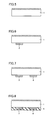
Fig. 1 is a schematic cross-sectional view for illustrating a part of the manufacturing process of an example of a method for manufacturing a solar cell according to the present invention. -
Fig. 2 is a schematic cross-sectional view for illustrating a part of the manufacturing process of the example of the method for manufacturing the solar cell according to the present invention. -
Fig. 3 is a schematic cross-sectional view for illustrating a part of the manufacturing process of the example of the method for manufacturing the solar cell according to the present invention. -
Fig. 4 is a schematic cross-sectional view for illustrating a part of the manufacturing process of the example of the method for manufacturing the solar cell according to the present invention. -
Fig. 5 is a schematic cross-sectional view for illustrating a part of the manufacturing process of the example of the method for manufacturing the solar cell according to the present invention. -
Fig. 6 is a schematic cross-sectional view for illustrating a part of the manufacturing process of the example of the method for manufacturing the solar cell according to the present invention. -
Fig. 7 is a schematic cross-sectional view for illustrating a part of the manufacturing process of the example of the method for manufacturing the solar cell according to the present invention. -
Fig. 8 is a schematic cross-sectional view for illustrating a part of the manufacturing process of the example of the method for manufacturing the solar cell according to the present invention. -
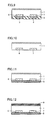
Fig. 9 is a schematic cross-sectional view for illustrating a part of the manufacturing process of the example of the method for manufacturing the solar cell according to the present invention. -
Fig. 10 is a schematic cross-sectional view for illustrating a part of the manufacturing process of the example of the method for manufacturing the solar cell according to the present invention. -
Fig. 11 is a schematic cross-sectional view for illustrating a part of the manufacturing process of the example of the method for manufacturing the solar cell according to the present invention. -
Fig. 12 is a schematic cross-sectional view for illustrating a part of the manufacturing process of the example of the method for manufacturing the solar cell according to the present invention. -
Fig. 13 is a schematic cross-sectional view for illustrating a part of the manufacturing process of the example of the method for manufacturing the solar cell according to the present invention. -
Fig. 14 is a schematic cross-sectional view for illustrating a part of the manufacturing process of the example of the method for manufacturing the solar cell according to the present invention. -
Fig. 15 is a schematic cross-sectional view of a conventional back electrode type solar cell. - 1, 110 n-type silicon substrate, 2 protective film, 3, 4 diffusing agent, 5 protective layer, 6 n+ diffusion layer, 7 p+ diffusion layer, 8, 111, 118
passivation film 9 antireflection film, 10, 115 n electrode, 11, 114 p electrode, 112 p-type doping region, 113 n-type doping region, 116, 117 contact hole. - The embodiments of the present invention will be hereinafter described. In addition, in the accompanying drawings of the present invention, the same or corresponding components are designated by the same reference characters.
- Referring to the schematic cross-sectional views in
Figs. 1-14 , an example of the method for manufacturing a solar cell according to the present invention will then be described. - First, as shown in
Fig. 1 , a damage layer la on the surface of an n-type silicon substrate 1 is etched, for example, by using an acid or alkaline solution and removed as shown inFig. 2 . - Then, as shown in
Fig. 3 , aprotective film 2 made, for example, of a silicon oxide film or a silicon nitride film is formed on one surface of n-type silicon substrate 1. In this case,protective film 2 made of the silicon oxide film can be formed, for example, by the atmospheric pressure CVD method performed using silane gas and oxygen.
Also,protective film 2 made of the silicon nitride film can be formed, for example, by the plasma CVD method performed using silane gas, ammonia gas and nitrogen gas. - Then, as shown in
Fig. 4 , a fine concavo-convex structure referred to as a texture structure is formed on the surface of n-type silicon substrate 1 whereprotective film 2 is not formed. In this case, the texture structure can be formed, for example, by immersing n-type silicon substrate 1 havingprotective film 2 formed thereon in the solution of about 80 °C containing potassium hydroxide and isopropyl alcohol (IPA). - Then, as shown in
Fig. 5 , n-type silicon substrate 1 is immersed in hydrofluoric acid to thereby etch and removeprotective film 2. - Although the texture structure is formed only on one surface of n-
type silicon substrate 1 in the above description, the texture structure may be formed on both surfaces of n-type silicon substrate 1 in the present invention. Furthermore, it is preferable that the plane orientation of the surface on which the texture structure is formed is (100). In addition, the process of forming the above-described texture structure may be performed after formation of the diffusion layer described below. - Then, an n+ diffusion layer and a p+ diffusion layer are selectively formed in the same surface of n-
type silicon substrate 1. As shown inFig. 6 , a diffusingagent 3 containing n-type impurities is applied onto a part of the surface of n-type silicon substrate 1 exposed by removingprotective film 2. In this case, it is preferable that application of diffusingagent 3 containing n-type impurities is carried out by printing using the screen printing method, the gravure printing method, the inkjet printing method, or the like because diffusingagent 3 containing n-type impurities can be selectively applied onto the surface of n-type silicon substrate 1. - As shown in
Fig. 7 , in the same surface as that of n-type silicon substrate 1 onto which diffusingagent 3 containing n-type impurities is applied, a diffusingagent 4 containing p-type impurities is then applied onto a portion spaced at a predetermined distance from the position where diffusingagent 3 containing n-type impurities is formed. In this case, it is preferable that application of diffusingagent 4 containing p-type impurities is also carried out by printing using the screen printing method, the gravure printing method, the inkjet printing method, or the like because diffusingagent 4 containing p-type impurities can be selectively applied onto the surface of n-type silicon substrate 1. - It is to be noted that diffusing
agent 3 containing n-type impurities may be formed of any component that allows diffusion of the n-type impurities, and it can be formed of components containing, for example, a silicon compound, an organic solvent and a thickening agent, except for n-type impurities. - Furthermore, diffusing
agent 4 containing p-type impurities may be formed of any component that allows diffusion of the p-type impurities, and it can be formed of components containing, for example, a silicon compound, an organic solvent and a thickening agent, except for p-type impurities. - As for the silicon compound which may be contained in diffusing
agent 3 containing n-type impurities and/or diffusingagent 4 containing p-type impurities, for example, tetramethoxysilane, tetraethoxysilane, tetrabutoxysilane, tetrapropoxysilane, and the like can be used alone or in combination thereof, which more specifically includes silane having a longer alkyl chain, silane having various alkyl residues, or the like. - Furthermore, as for the organic solvent which may be contained in diffusing
agent 3 containing n-type impurities and/or diffusingagent 4 containing p-type impurities, for example, ethylene glycol monomethyl ether, propylene glycol monomethyl ether or the like can be used. - Furthermore, as for the thickening agent which may be contained in diffusing
agent 3 containing n-type impurities and/or diffusingagent 4 containing p-type impurities, for example, a cellulose compound, polyvinyl pyrrolidone, gelatin or the like can be used. - Furthermore, in the above description, it is preferable to use, for example, phosphorus and/or a phosphorus compound as n-type impurities contained in diffusing
agent 3 that contains n-type impurities. It is also preferable to use, for example, boron and/or a boron compound as p-type impurities contained in diffusingagent 4 that contains p-type impurities. - It is preferable that the viscosity of each of the above-described
diffusing agents agent 3 and diffusingagent 4. - In addition, after application of diffusing
agent 3 and diffusingagent 4, each of diffusingagents agent 3 and diffusingagent 4 can be dried, for example, by heating these applied diffusingagents agent 3 and diffusingagent 4 are heated to a temperature of about 200 °C, a volatile component contained in each of diffusingagent 3 and diffusingagent 4 can be removed in advance. Furthermore, it may also be that, after one of diffusingagents - Furthermore, after diffusing
agent 3 and diffusingagent 4 are dried, each of diffusingagents agent 3 and diffusingagent 4 are baked by heating these diffusingagents - The baking process carried out as described above allows solidification and/or densification of diffusing
agent 3 and diffusingagent 4, and also allows the baking process to be eliminated when diffusingagent 3 and diffusingagent 4 are solidified by the drying process. It is to be noted that the order in which diffusingagent 3 and diffusingagent 4 are applied may be reversed in the above description. - As shown in
Fig. 8 , on the surface of n-type silicon substrate 1 on which diffusingagent 3 and diffusingagent 4 are formed, aprotective layer 5 is then formed so as to cover diffusingagent 3 and diffusingagent 4. Althoughprotective layer 5 is formed so as to cover both of diffusingagent 3 and diffusingagent 4 in the present embodiment, it only needs to be formed so as to cover at least one of diffusingagent 3 and diffusingagent 4 in the present invention. In other words, sinceprotective layer 5 covers one of diffusingagent 3 and diffusingagent 4, the impurities can be effectively prevented from entering the other diffusion region. - Furthermore, it is preferable that
protective layer 5 is formed so as to cover the entire surface of n-type silicon substrate 1 on which diffusingagent 3 and diffusingagent 4 are formed. Sinceprotective layer 5 is formed so as to cover the entire surface of n-type silicon substrate 1, the impurities can be effectively prevented from entering the area other than the diffusion region. - Furthermore, while no particular limitation is imposed on
protective layer 5 as long as it performs a function of preventing entrance of n-type impurities and/or p-type impurities, it is preferable to use a silicon oxide film. The silicon oxide film used asprotective layer 5 can be formed using an oxidizing agent. For example, in the case where the paste containing a silicon compound, an organic solvent, a thickening agent, and the like is used as an oxidizing agent,protective layer 5 can be formed by applying the oxidizing agent by spin coating, the screen printing method, the gravure printing method, the inkjet printing method, or the like. It is also preferable that the viscosity of the oxidizing agent used for formingprotective layer 5 can be adjusted and the viscosity is adjusted in accordance with the application method. Furthermore, the application method can also be selected in accordance with the viscosity of the oxidizing agent. - It is to be noted that, in addition to the method performed using the oxidizing agent,
protective layer 5 made of a silicon oxide film can also be formed, for example, using silane gas and oxygen gas by the atmospheric pressure CVD method. - Furthermore, it is preferable that
protective layer 5 made of the above-described silicon oxide film has a thickness of 200 nm or more.Protective layer 5 having a thickness of 200 nm or more tends to be effective for preventing the impurities of diffusingagent 3 and diffusingagent 4 from entering another region in the heat treatment described below. - Then, when n-
type silicon substrate 1 havingprotective layer 5 formed thereon is subjected to heat treatment, as shown inFig. 9 , the n-type impurities are diffused from diffusingagent 3 to form ann+ diffusion layer 6 in the surface of n-type silicon substrate 1, and the p-type impurities are diffused from diffusingagent 4 to form ap+ diffusion layer 7 in the surface of n-type silicon substrate 1. - In this case, it is preferable that the heat treatment is performed at a temperature of 800 °C or higher and 1100 °C or lower. In the case where the heat treatment is performed at a temperature of 800 °C or higher and 1100 °C or lower, the electrical characteristics of the solar cell according to the present invention tends to be enhanced. Each concentration of the n-type impurities in
n+ diffusion layer 6 and the p-type impurities inp+ diffusion layer 7 tends to be increased in proportion to the level of the heat treatment temperature. Accordingly, the concentration of the impurities in the diffusion layer is decreased when this heat treatment temperature is lower than 800 °C, and the concentration of the impurities in the diffusion layer is increased when this heat treatment temperature is higher than 1100 °C. Thus, the electrical characteristics of the solar cell according to the present invention is more likely to be degraded both in the case where the heat treatment temperature is lower than 800 °C and higher than 1100 °C. - Also in the present invention, for example, as shown in
Fig. 9 , it is preferable thatn+ diffusion layer 6 andp+ diffusion layer 7 are formed so as to be spaced apart from each other such that the region having the same conductivity type as that of n-type silicon substrate 1 (that is, the region of n-type silicon substrate 1) is formed betweenn+ diffusion layer 6 andp+ diffusion layer 7. In order to formn+ diffusion layer 6 andp+ diffusion layer 7 so as to be spaced apart from each other, it is preferable that diffusingagent 3 and diffusingagent 4 are applied onto the surface of n-type silicon substrate 1 so as to be spaced apart from each other. - Then, as shown in
Fig. 10 ,protective layer 5 is removed. For example, in the case whereprotective layer 5 is a glass layer, it is preferable to removeprotective layer 5 by using HF (hydrofluoric acid). - Then, as shown in
Fig. 11 , apassivation film 8 is formed on the surface of n-type silicon substrate 1 on whichn+ diffusion layer 6 andp+ diffusion layer 7 are formed. In this case, for example, a silicon oxide film, a silicon nitride film, a multilayer film thereof or the like can be used aspassivation film 8. The silicon oxide film formingpassivation film 8 can be formed, for example, by the thermal oxidation method or the atmospheric pressure CVD method. The silicon nitride film formingpassivation film 8 can be formed, for example, by the plasma CVD method. Furthermore, the surface of n-type silicon substrate 1 may be washed by the conventionally known method prior to formation ofpassivation film 8. - Then, as shown in
Fig. 12 , anantireflection film 9 is formed on the surface of n-type silicon substrate 1 on which the texture structure is formed. In this case, for example, a nitride film formed by the plasma CVD method can be used asantireflection film 9. The nitride film formingantireflection film 9 may include, for example, a multilayer film formed of a nitride film having a refractive index of approximately 2.4 to 3.2 (particularly, a refractive index of 2.9 or more and 3.2 or less) and a nitride film having a refractive index of approximately 1.9 to 2.2 or a single layer film formed of a film having a refractive index of approximately 1.9 to 2.2. - Then, as shown in
Fig. 13 ,passivation film 8 is partially removed to expose a part of the surface of each ofn+ diffusion layer 6 andp+ diffusion layer 7. In this case, partial removal ofpassivation film 8 can be carried out, for example, by placing the conventionally known etching paste on the surface ofpassivation film 8 and heating the etching paste, for example, at a temperature of 200 °C to 400 °C, which is followed by washing with water. - Then, as shown in
Fig. 14 , ann electrode 10 anda p electrode 11 are formed on the surfaces ofn+ diffusion layer 6 andp+ diffusion layer 7, respectively, to produce a back electrode type solar cell. In this case,n electrode 10 andp electrode 11 can be formed, for example, by applying the electrode material containing silver onto the exposed surface of each ofn+ diffusion layer 6 andp+ diffusion layer 7, which is then dried and/or baked. In addition,n electrode 10 andp electrode 11 can also be formed by using the vapor deposition method. - In the present invention, the n+ diffusion layer and the p+ diffusion layer are formed by the heat treatment performed in the state where the diffusing agent containing n-type impurities and/or the diffusing agent containing p-type impurities are/is covered by a protective layer. This can prevent production of the solar cell in the state where the n-type impurities and the p-type impurities diffuse into the area where diffusion of the impurities is not required during formation of these diffusion layers. Consequently, the degradation of the electrical characteristics of the solar cell resulting from diffusion of these impurities can be effectively suppressed.
- Therefore, according to the present invention, a solar cell having high electrical characteristics can be produced with stability.
- Although the case where an n-type silicon substrate is used as a semiconductor substrate has been set forth in the above description, a semiconductor substrate other than the n-type silicon substrate, for example, a p-type silicon substrate and the like, can also be used in the present invention.
- Furthermore, although the case where a silicon oxide film is used as an oxide film has been set forth in the above description, the oxide film is not limited to a silicon oxide film in the present invention.
- Furthermore, although the case where a silicon nitride film is used as a nitride film has been set forth in the above description, the nitride film is not limited to a silicon nitride film in the present invention.
- Furthermore, although the case of a back electrode type solar cell has been mainly set forth in the above description, the present invention is not limited to a back electrode type solar cell, but can also be applied to the solar cell such as a double-sided electrode type solar cell other than the back electrode type solar cell. Example
- First, an n-
type silicon substrate 1 in which the surface has a plane orientation of (100) was prepared as a semiconductor substrate (Fig. 1 ). Then, a damage layer la on the surface of n-type silicon substrate 1 was removed by etching by using the alkaline solution (Fig. 2 ). - Then, a
protective film 2 made of a silicon oxide film was formed by the atmospheric pressure CVD method as a texture-preventing mask (Fig. 3 ). Then, n-type silicon substrate 1 havingprotective film 2 formed thereon was immersed in the solution containing potassium hydroxide and isopropyl alcohol (IPA) at approximately 80°C, to form a texture structure on one surface of n-type silicon substrate 1 (Fig. 4 ). It was then immersed in hydrofluoric acid to removeprotective film 2 of n-type silicon substrate 1 (Fig. 5 ). - Then, a diffusing
agent 3 made of a phosphorus compound, a silicon compound, an organic solvent, and a thickening agent was partially applied onto the surface of the n-type silicon substrate by screen printing, and dried by heating to a temperature of 200 °C under nitrogen atmosphere (Fig. 6 ). Then, in the same surface as that of n-type silicon substrate 1 onto which diffusingagent 3 containing a phosphorus compound was applied, a diffusingagent 4 made of a boron compound, a silicon compound, an organic solvent, and a thickening agent was partially applied by screen printing so as to be spaced apart from the region where the diffusing agent containing a phosphorus compound was applied. This is followed by heating to 200 °C under nitrogen atmosphere for drying (Fig. 7 ). Then, diffusingagent 3 and diffusingagent 4 were solidified and densified by baking for 10 minutes under oxygen atmosphere at 400 °C. - Then, on the entire surface of n-
type silicon substrate 1 onto which diffusingagent 3 and diffusingagent 4 were applied, a silicon oxide film was formed by the atmospheric pressure CVD method to have a thickness of 300 nm as a protective layer 5 (Fig. 8 ). Then, n-type silicon substrate 1 havingprotective layer 5 formed thereon was introduced into a quartz furnace raised to a temperature of approximately 950 °C and held for 50 minutes, to diffuse phosphorus and boron into n-type silicon substrate 1, with the result that ann+ diffusion layer 6 and ap+ diffusion layer 7 were formed so as to be spaced apart from each other (Fig. 9 ). After formation ofn+ diffusion layer 6 andp+ diffusion layer 7, the glass layer remaining on the surface of n-type silicon substrate 1 was removed by hydrofluoric acid (Fig. 10 ). - Then, the mixed solution of water, hydrochloric acid and hydrogen peroxide solution was heated to approximately 70 °C, in which n-
type silicon substrate 1 having the glass layer removed therefrom was immersed, to wash the surface of n-type silicon substrate 1. The surface of n-type silicon substrate 1 was then immersed in hydrofluoric acid for hydrofluoric acid treatment. Then, n-type silicon substrate 1 was introduced into the quartz furnace raised to a temperature of 850 °C under oxygen atmosphere and held for 30 minutes, to form a thermal oxide film on the surface of n-type silicon substrate 1. Then, a silicon oxide film was formed to have a thickness of 200 nm by the atmospheric pressure CVD method, to form apassivation film 8 on the surface of the n-type silicon substrate which had been subjected to the hydrofluoric acid treatment (Fig. 11 ). - Then, an
antireflection film 9 made of a silicon nitride film was formed by the plasma CVD method on the surface of the n-type silicon substrate on which the texture structure was formed. In this case,antireflection film 9 was made of a multilayer film including a silicon nitride film having a refractive index of 3.2 and a silicon nitride film having a refractive index of 2.1 (Fig. 12 ). - The etching paste containing phosphoric acid as a main component was printed by the screen printing method on the surface area of
passivation film 8 corresponding to the position where each ofn+ diffusion layer 6 andp+ diffusion layer 7 was formed. The etching paste was subsequently heated for 2 minutes by the hot plate heated to 330 °C. The residue remaining on the surface of the passivation film was washed away by ultrasonic washing with water to expose the surface of each ofn+ diffusion layer 6 and p+ diffusion layer 7 (Fig. 13 ). - Then, a silver paste was printed on the exposed surface of each of
n+ diffusion layer 6 andp+ diffusion layer 7. Further, n-type silicon substrate 1 having the silver paste printed thereon was passed through a drying furnace, and baked by heating at a temperature of 500 °C (Fig. 14 ). This resulted in formation of ann electrode 10 electrically connecting ton+ diffusion layer 6 anda p electrode 11 electrically connecting top+ diffusion layer 7. - According to the above-described processes, the back electrode type solar cell according to the example of the configuration shown in
Fig. 14 was produced. - In addition, a back electrode type solar cell was produced as a comparative example in a similar manner to the example except that the protective layer was not entirely formed on the surface of the n-type silicon substrate onto which the diffusing agent was applied.
- With regard to the back electrode type solar cell according to each of the example and the comparative example produced as described above, a short-circuit current Jsc (mA), an open circuit voltage Voc (V), a fill factor F.F, and a conversion efficiency Eff (%) were measured. The results are shown in Table 1.
[Table 1] Jsc (mA) Voc (V) F.F Eff (%) Example 37.4 0.642 0.765 18.4 Comparative Example 36.5 0.641 0.69 16.1 - As shown in Table 1, the back electrode type solar cell according to the example tends to have excellent electrical characteristics regarding all of short-circuit current Jsc, open circuit voltage Voc, fill factor F.F, and conversion efficiency Eff, as compared to the back electrode type solar cell according to the comparative example.
- It is considered that this is because diffusion of the n-type impurities and the p-type impurities occurs without formation of a protective layer in the back electrode type solar cell according to the comparative example, which causes diffusion of both of the n-type impurities and the p-type impurities to thereby prevent separation of the n+ diffusion layer and the p+ diffusion layer, leading to leakage of the current, with the result that the electrical characteristics degrade as compared to the back electrode type solar cell according to the example.
- It should be understood that the embodiments and the examples disclosed herein are illustrative and non-restrictive in every respect. The scope of the present invention is defined by the terms of the claims, rather than the description above, and is intended to include any modifications within the scope and meaning equivalent to the terms of the claims.
- According to the present invention, a method for manufacturing a solar cell which allows stable production of a solar cell having high electrical characteristics can be provided.
Claims (9)
- A method for manufacturing a solar cell, comprising the steps of:applying a first diffusing agent (3) containing n-type impurities and a second diffusing agent (4) containing p-type impurities onto a semiconductor substrate (1);forming a protective layer (5) covering at least one of said first diffusing agent (3) and said second diffusing agent (4); anddiffusing at least one of the n-type impurities and the p-type impurities in a surface of said semiconductor substrate (1) by heat treatment of said semiconductor substrate (1) having said protective layer (5) formed thereon.
- The method for manufacturing a solar cell according to claim 1, wherein said n-type impurities include at least one of phosphorus and a phosphorus compound, and said p-type impurities include at least one of boron and a boron compound.
- The method for manufacturing a solar cell according to claim 1, wherein at least one of said first diffusing agent (3) and said second diffusing agent (4) is applied by printing.
- The method for manufacturing a solar cell according to claim 1, wherein at least one of said first diffusing agent (3) and said second diffusing agent (4) is baked prior to formation of said protective layer (5).
- The method for manufacturing a solar cell according to claim 1, wherein said protective layer (5) is an oxide film.
- The method for manufacturing a solar cell according to claim 5, wherein said oxide film has a film thickness of 200 nm or more.
- The method for manufacturing a solar cell according to claim 1, wherein said heat treatment is performed at a temperature of 800 °C or higher and 1100 °C or lower.
- The method for manufacturing a solar cell according to claim 1, wherein said n-type impurities and said p-type impurities are diffused in a same surface of said semiconductor substrate (1).
- The method for manufacturing a solar cell according to claim 8, wherein said semiconductor substrate (1) is an n-type, and an n+ diffusion layer (6) formed by diffusing said n-type impurities and a p+ diffusion layer (7) formed by diffusing said p-type impurities are formed so as to be spaced apart from each other.
Applications Claiming Priority (2)
| Application Number | Priority Date | Filing Date | Title |
|---|---|---|---|
| JP2007242137A JP5236914B2 (en) | 2007-09-19 | 2007-09-19 | Manufacturing method of solar cell |
| PCT/JP2008/065505 WO2009037955A1 (en) | 2007-09-19 | 2008-08-29 | Method for manufacturing solar cell |
Publications (1)
| Publication Number | Publication Date |
|---|---|
| EP2197036A1 true EP2197036A1 (en) | 2010-06-16 |
Family
ID=40467775
Family Applications (1)
| Application Number | Title | Priority Date | Filing Date |
|---|---|---|---|
| EP08832041A Withdrawn EP2197036A1 (en) | 2007-09-19 | 2008-08-29 | Method for manufacturing solar cell |
Country Status (4)
| Country | Link |
|---|---|
| US (1) | US20100190286A1 (en) |
| EP (1) | EP2197036A1 (en) |
| JP (1) | JP5236914B2 (en) |
| WO (1) | WO2009037955A1 (en) |
Cited By (2)
| Publication number | Priority date | Publication date | Assignee | Title |
|---|---|---|---|---|
| CN102593259A (en) * | 2011-11-30 | 2012-07-18 | 友达光电股份有限公司 | How to Make a Solar Cell |
| US9406821B2 (en) | 2010-03-04 | 2016-08-02 | Sunpower Corporation | Method of fabricating a back-contact solar cell and device thereof |
Families Citing this family (25)
| Publication number | Priority date | Publication date | Assignee | Title |
|---|---|---|---|---|
| DE112009000788T5 (en) * | 2008-04-25 | 2011-04-21 | ULVAC, Inc., Chigasaki-shi | Production process for solar cells, production device for solar cells and solar cell |
| DE102009005168A1 (en) * | 2009-01-14 | 2010-07-22 | Fraunhofer-Gesellschaft zur Förderung der angewandten Forschung e.V. | Solar cell and method for producing a solar cell from a silicon substrate |
| KR101135591B1 (en) * | 2009-03-11 | 2012-04-19 | 엘지전자 주식회사 | Solar cell and solar cell module |
| KR101588456B1 (en) * | 2009-06-19 | 2016-02-12 | 엘지전자 주식회사 | Solar cell and manufacturing mehtod of the same |
| KR101588458B1 (en) * | 2009-07-16 | 2016-01-25 | 엘지전자 주식회사 | Solar cell and manufacturing method thereof |
| KR101139459B1 (en) | 2009-08-27 | 2012-04-30 | 엘지전자 주식회사 | Sollar Cell And Fabrication Method Thereof |
| JP5555469B2 (en) * | 2009-10-05 | 2014-07-23 | 東京応化工業株式会社 | Diffusion agent composition and method for forming impurity diffusion layer |
| JP2011187894A (en) * | 2010-03-11 | 2011-09-22 | Sharp Corp | Coating liquid for diffusing phosphor dopant, coating film formed by the same, and method for manufacturing solar cell |
| CN102244137A (en) * | 2010-05-14 | 2011-11-16 | 北京北方微电子基地设备工艺研究中心有限责任公司 | Solar cell and manufacturing method thereof |
| US8377738B2 (en) * | 2010-07-01 | 2013-02-19 | Sunpower Corporation | Fabrication of solar cells with counter doping prevention |
| KR20120009682A (en) | 2010-07-20 | 2012-02-02 | 삼성전자주식회사 | Solar cell manufacturing method |
| EP2642528A1 (en) * | 2010-11-17 | 2013-09-25 | Hitachi Chemical Co., Ltd. | Method for producing solar cell |
| EP2642529A4 (en) * | 2010-11-17 | 2017-10-18 | Hitachi Chemical Company, Ltd. | Method for producing photovoltaic cell |
| JP5802407B2 (en) * | 2011-03-04 | 2015-10-28 | 三菱瓦斯化学株式会社 | Substrate processing apparatus and substrate processing method |
| KR101724005B1 (en) * | 2011-04-29 | 2017-04-07 | 삼성에스디아이 주식회사 | Solar cell and its manufacturing method |
| JP5756352B2 (en) * | 2011-06-21 | 2015-07-29 | シャープ株式会社 | Manufacturing method of back electrode type solar cell |
| JP5897269B2 (en) * | 2011-06-28 | 2016-03-30 | 日本酢ビ・ポバール株式会社 | Phosphorus diffusion coating solution |
| JP5176159B1 (en) * | 2011-07-19 | 2013-04-03 | 日立化成株式会社 | N-type diffusion layer forming composition, n-type diffusion layer manufacturing method, and solar cell element manufacturing method |
| US9412895B2 (en) | 2012-04-04 | 2016-08-09 | Samsung Sdi Co., Ltd. | Method of manufacturing photoelectric device |
| KR101397024B1 (en) * | 2012-04-04 | 2014-05-21 | 삼성에스디아이 주식회사 | Method of manufacturing for photovoltaic device |
| WO2013157090A1 (en) * | 2012-04-18 | 2013-10-24 | 株式会社日立製作所 | Solar cell and producing method therefor |
| CN105122461B (en) * | 2013-04-24 | 2018-03-02 | 三菱电机株式会社 | Manufacturing method of solar cell |
| JP2016066771A (en) * | 2014-09-17 | 2016-04-28 | 日立化成株式会社 | Method for manufacturing solar cell element |
| JP6559326B2 (en) * | 2016-03-14 | 2019-08-14 | 三菱電機株式会社 | Manufacturing method of solar cell |
| CN110890443B (en) * | 2018-09-10 | 2023-01-31 | 浙江清华柔性电子技术研究院 | Crystalline silicon solar cell diffusion layer and preparation method thereof |
Family Cites Families (17)
| Publication number | Priority date | Publication date | Assignee | Title |
|---|---|---|---|---|
| US4104091A (en) * | 1977-05-20 | 1978-08-01 | The United States Of America As Represented By The Administrator Of The National Aeronautics And Space Administration | Application of semiconductor diffusants to solar cells by screen printing |
| US4927770A (en) * | 1988-11-14 | 1990-05-22 | Electric Power Research Inst. Corp. Of District Of Columbia | Method of fabricating back surface point contact solar cells |
| JPH02177569A (en) * | 1988-12-28 | 1990-07-10 | Sharp Corp | Manufacture of solar cell |
| US6552414B1 (en) * | 1996-12-24 | 2003-04-22 | Imec Vzw | Semiconductor device with selectively diffused regions |
| EP0851511A1 (en) * | 1996-12-24 | 1998-07-01 | IMEC vzw | Semiconductor device with two selectively diffused regions |
| JP2000091254A (en) * | 1998-09-11 | 2000-03-31 | Oki Electric Ind Co Ltd | METHOD FOR DIFFUSING SOLID PHASE OF Zn AND LIGHT EMITTING ELEMENT USING THE SAME |
| JP2000183379A (en) * | 1998-12-11 | 2000-06-30 | Sanyo Electric Co Ltd | Method for manufacturing solar cell |
| DE19910816A1 (en) * | 1999-03-11 | 2000-10-05 | Merck Patent Gmbh | Doping pastes for producing p, p + and n, n + regions in semiconductors |
| JP2002124692A (en) * | 2000-10-13 | 2002-04-26 | Hitachi Ltd | Solar cell and method of manufacturing the same |
| EP1449261B1 (en) * | 2001-11-26 | 2007-07-25 | Shell Solar GmbH | SOLAR CELL WITH BACKSIDE CONTACTS and its manufacturing method |
| JP2004221149A (en) * | 2003-01-10 | 2004-08-05 | Hitachi Ltd | Solar cell manufacturing method |
| US20060060238A1 (en) * | 2004-02-05 | 2006-03-23 | Advent Solar, Inc. | Process and fabrication methods for emitter wrap through back contact solar cells |
| JP2006041105A (en) * | 2004-07-26 | 2006-02-09 | Sharp Corp | Solar cell and method for manufacturing the same |
| WO2006075426A1 (en) * | 2004-12-27 | 2006-07-20 | Naoetsu Electronics Co., Ltd. | Back junction solar cell and process for producing the same |
| JP4481869B2 (en) * | 2005-04-26 | 2010-06-16 | 信越半導体株式会社 | SOLAR CELL MANUFACTURING METHOD, SOLAR CELL, AND SEMICONDUCTOR DEVICE MANUFACTURING METHOD |
| JP2006310368A (en) * | 2005-04-26 | 2006-11-09 | Shin Etsu Handotai Co Ltd | Solar cell manufacturing method and solar cell |
| FR2906405B1 (en) * | 2006-09-22 | 2008-12-19 | Commissariat Energie Atomique | METHOD OF MAKING DOPED REGIONS IN A SUBSTRATE AND PHOTOVOLTAIC CELL |
-
2007
- 2007-09-19 JP JP2007242137A patent/JP5236914B2/en not_active Expired - Fee Related
-
2008
- 2008-08-29 WO PCT/JP2008/065505 patent/WO2009037955A1/en not_active Ceased
- 2008-08-29 EP EP08832041A patent/EP2197036A1/en not_active Withdrawn
- 2008-08-29 US US12/678,592 patent/US20100190286A1/en not_active Abandoned
Non-Patent Citations (1)
| Title |
|---|
| See references of WO2009037955A1 * |
Cited By (2)
| Publication number | Priority date | Publication date | Assignee | Title |
|---|---|---|---|---|
| US9406821B2 (en) | 2010-03-04 | 2016-08-02 | Sunpower Corporation | Method of fabricating a back-contact solar cell and device thereof |
| CN102593259A (en) * | 2011-11-30 | 2012-07-18 | 友达光电股份有限公司 | How to Make a Solar Cell |
Also Published As
| Publication number | Publication date |
|---|---|
| WO2009037955A1 (en) | 2009-03-26 |
| JP2009076546A (en) | 2009-04-09 |
| US20100190286A1 (en) | 2010-07-29 |
| JP5236914B2 (en) | 2013-07-17 |
Similar Documents
| Publication | Publication Date | Title |
|---|---|---|
| EP2197036A1 (en) | Method for manufacturing solar cell | |
| US8257994B2 (en) | Method for manufacturing solar cell by forming a high concentration P-type impurity diffusion layer | |
| KR101241617B1 (en) | Solar cell and method of manufacturing the same | |
| EP3151286B1 (en) | Solar cell element, method for manufacturing same and solar cell module | |
| KR101452881B1 (en) | Back contact solar cell and method for manufacturing back contact solar cell | |
| US20100218826A1 (en) | Method for producing a silicon solar cell with a back-etched emitter as well as a corresponding solar cell | |
| JP5215330B2 (en) | Manufacturing method of back electrode type solar cell, back electrode type solar cell and back electrode type solar cell module | |
| EP2405486A1 (en) | Process for producing semiconductor device | |
| JP2007235174A (en) | Photocell having selective diffusion region | |
| JP2010161310A (en) | Backside electrode type solar cell and method of manufacturing the same | |
| EP2626914A2 (en) | Solar Cell and Method of Manufacturing the Same | |
| JP2012023228A (en) | Method and device of manufacturing solar cell | |
| KR101464001B1 (en) | Manufacturing method of solar cell and etching paste | |
| JP5139502B2 (en) | Back electrode type solar cell | |
| JP2006156646A (en) | Manufacturing method of solar cell | |
| KR20190073362A (en) | Method for manufacturing high photoelectric conversion efficiency solar cell and high photoelectric conversion efficiency solar cell | |
| JP5165906B2 (en) | Method for manufacturing photoelectric conversion element | |
| KR101464002B1 (en) | Manufacturing method of solar cell | |
| CN104521002B (en) | Manufacturing method of solar cell | |
| JP4632672B2 (en) | Manufacturing method of solar cell | |
| JP2004281569A (en) | Method for manufacturing solar cell element | |
| EP3702048B1 (en) | Method for drying polyimide paste and method for producing solar cells capable of highly-efficient photoelectric conversion | |
| KR101321538B1 (en) | Bulk silicon solar cell and method for producing same | |
| EP3217437B1 (en) | Solar cell and method for manufacturing same | |
| KR100378347B1 (en) | Method of manufacturing recessed electrode type solar cell |
Legal Events
| Date | Code | Title | Description |
|---|---|---|---|
| PUAI | Public reference made under article 153(3) epc to a published international application that has entered the european phase |
Free format text: ORIGINAL CODE: 0009012 |
|
| 17P | Request for examination filed |
Effective date: 20100324 |
|
| AK | Designated contracting states |
Kind code of ref document: A1 Designated state(s): AT BE BG CH CY CZ DE DK EE ES FI FR GB GR HR HU IE IS IT LI LT LU LV MC MT NL NO PL PT RO SE SI SK TR |
|
| AX | Request for extension of the european patent |
Extension state: AL BA MK RS |
|
| RIN1 | Information on inventor provided before grant (corrected) |
Inventor name: FUNAKOSHI, YASUSHI Inventor name: KOHIRA, MASATSUGU |
|
| DAX | Request for extension of the european patent (deleted) | ||
| STAA | Information on the status of an ep patent application or granted ep patent |
Free format text: STATUS: THE APPLICATION HAS BEEN WITHDRAWN |
|
| 18W | Application withdrawn |
Effective date: 20130328 |