EP2192687A2 - Amplifier and amplifier switch with switched capacity - Google Patents
Amplifier and amplifier switch with switched capacity Download PDFInfo
- Publication number
- EP2192687A2 EP2192687A2 EP09014521A EP09014521A EP2192687A2 EP 2192687 A2 EP2192687 A2 EP 2192687A2 EP 09014521 A EP09014521 A EP 09014521A EP 09014521 A EP09014521 A EP 09014521A EP 2192687 A2 EP2192687 A2 EP 2192687A2
- Authority
- EP
- European Patent Office
- Prior art keywords
- amplifier
- compensation
- switch
- frequency compensation
- capacity
- Prior art date
- Legal status (The legal status is an assumption and is not a legal conclusion. Google has not performed a legal analysis and makes no representation as to the accuracy of the status listed.)
- Granted
Links
- 238000000034 method Methods 0.000 claims abstract description 4
- 239000003990 capacitor Substances 0.000 claims description 58
- 238000011144 upstream manufacturing Methods 0.000 claims description 13
- 101100260207 Schizosaccharomyces pombe (strain 972 / ATCC 24843) sfc2 gene Proteins 0.000 claims description 4
- 230000000694 effects Effects 0.000 claims description 4
- 101100113692 Caenorhabditis elegans clk-2 gene Proteins 0.000 claims description 3
- 230000003321 amplification Effects 0.000 description 6
- 238000003199 nucleic acid amplification method Methods 0.000 description 6
- 230000001052 transient effect Effects 0.000 description 4
- 238000005457 optimization Methods 0.000 description 2
- 230000003071 parasitic effect Effects 0.000 description 2
- 230000001960 triggered effect Effects 0.000 description 2
- 238000010276 construction Methods 0.000 description 1
- 230000001419 dependent effect Effects 0.000 description 1
- 238000005516 engineering process Methods 0.000 description 1
- 239000004065 semiconductor Substances 0.000 description 1
Images

Classifications
-
- H—ELECTRICITY
- H03—ELECTRONIC CIRCUITRY
- H03F—AMPLIFIERS
- H03F1/00—Details of amplifiers with only discharge tubes, only semiconductor devices or only unspecified devices as amplifying elements
- H03F1/42—Modifications of amplifiers to extend the bandwidth
Definitions
- the invention relates to an amplifier for a switched capacitor amplifier circuit having the above-mentioned features according to claim 1 or to such a switched capacitor amplifier circuit and such an amplifier.
- Switched capacitor circuits are used as amplifiers in many applications.
- An example is a use in a so-called pipeline analog-to-digital converter.
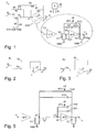
- Fig. 1 shows in the left, not shown enlarged figure portion a particular form of an amplifier arrangement with an amplifier circuit IC.
- the amplifier arrangement is designed with switched capacitance Cf, Cs and is also referred to below as a switched capacitor amplifier.
- reset configuration English reset / German: reset
- problems can be avoided by an offset (German: offset) of an amplifier used therein V, since this offset in a first clock phase ⁇ 1 of two clock phases ⁇ 1, ⁇ 2 (English Clockphases) is stored and not in a second of the clock phases ⁇ 2 more than mistakes appear.
- a circuit input i to which an input voltage Vi is applied, leads to a first switch S1 and a second switch S2 connected in parallel therewith. These two switches S1, S2 can be driven to close by a first switching signal, which is applied in a first clock phase ⁇ 1.
- a first switchable capacitance Cs switched between the second switch S2 and the amplifier input node n.
- a negative set input of the amplifier V * is connected between the amplifier input node n and a circuit output node o. At the amplifier output node o results in an output voltage Vo.
- a positive input of the amplifier V is connected to a ground terminal or to a reference potential GND.
- the amplifier input node n is switchable via a third switch S3 parallel to the amplifier V to the amplifier output node o.
- the first switching signal ⁇ 1 can also be applied to it.
- a control voltage in the form of, for example, a digital / analog converter output voltage Vdac or another reference potential, such as a reference voltage Vcm can be applied to a node between the first switch S1 and the second switchable capacitance Cs via a fifth switch S5.
- a fifth switch S5 For the closing switching of the fifth switch S5 is a second switching signal, which is applied in the second clock phase ⁇ 2.
- a fourth switch S4 which is likewise triggered by means of the second switching signal, a node between the second switch S2 and the first switchable capacitance Cf is connectable to the amplifier output node o.
- control device X which is designed, inter alia, to provide the first and the second switching signal in the first and second clock phase ⁇ 1, ⁇ 2.
- the control takes place in a known manner.
- Fig. 2 outlines the capacitors and their capacitances CS and CF in parallel switched and by means of the first two in Fig. 1 outlined switches S1 and S2 connected to the circuit input i.
- the amplifier V is completely fed back by means of the third switch S3.
- the output voltage Vo and thus the voltage at the second node of the two capacitances Cs & Cf is the reference voltage Vcm, which is also referred to as common mode voltage plus the offset voltage Voff of the amplifier V.
- Vcm which is also referred to as common mode voltage plus the offset voltage Voff of the amplifier V.
- Fig. 3 outlines the first two first in Fig. 1 sketched switches S1 and S2 open.
- the fifth switch S5 is closed and connects the second switchable capacitance Cs with the reference voltage Vcm at a switched capacitor amplifier or with a digital / analogue converter output voltage Vdac in a pipeline analog-to-digital converter.
- the full feedback of the amplifier V is canceled because the third switch S3 is opened, and the first switchable capacitance Cf is connected to the output node o by means of the closed fourth switch S4 from the amplifier input node n of the amplifier V.
- the output voltage Vo in the second clock phase ⁇ 2 is thus compensated for by the amplified, negative input voltage Vi in the first clock phase ⁇ 1 , the offset voltage Voff.
- the amplification error Aerr becomes smaller the greater the gain A0 of the amplifier V is.
- OTA circuits i. Transconductance amplifier or current amplifier with operational amplification, used in conjunction with cascode circuits.
- the gain V0 can be further increased by using gain boosting circuits.
- the advantage of the one-stage arrangements is that high bandwidths are achieved, since additional measures for frequency compensation are not required.
- Fig. 6 shows a possible two-stage amplification arrangement of a frequency compensated amplifier V *.
- the compensation input node n2 Between the two amplifier stages V1, V2 there is a node, which is referred to below as the compensation input node n2.
- a first amplifier capacitance C1 and a first further resistor Ro1 are connected in parallel with one another.
- a load capacitance CL and a second further resistance Ro2 are connected in parallel with each other.
- the first amplifier capacitance C1 and the first further resistor Ro1 can already be formed by device properties.
- the first additional resistor Ro1 is the output resistance of the upstream amplifier stage V1 as the source of the real transconductance gm1
- the first amplifier capacitance C1 is the input capacitance of the second amplifier stage V2 with its transconductance gm2 and the parasitic load capacitance of the output of the upstream amplifier stage V1.
- An explicit placement of a first further resistor Ro1 or the first amplifier capacitance C1 does not have to, but can take place. Accordingly, if necessary, the existing parasitic elements are sufficient.
- a first compensation resistor RZ and a capacitance or total capacity for frequency compensation CC are connected in series between the compensation input node n2 and the amplifier output node o.
- the amplifier V * is only fed back to a smaller extent.
- Frequency compensation for multistage amplifiers must be designed in such a way that there is a stable control system in both clock phases ⁇ 1, ⁇ 2. Due to the larger feedback factor ⁇ ( ⁇ 1) during the first clock phase ⁇ 1, this phase is the decisive phase for the frequency compensation.
- Fig. 6 illustrates a possible frequency compensation for a second order amplification system, a so-called Miller compensation.
- ⁇ 1
- CL load capacitance
- g m1 and g m2 of the two amplifier stages V1, V2 a certain transit frequency f T , as can be seen from eg PE Allan, DR Holberg; CMOS analog circuit design; Oxford University Press; , 1987; ISBN 0-19-510720-9; page 374ff ; Section 8.2 etc. is known.
- the feedback factor ⁇ may be considerably lower.
- the feedback factor ⁇ is only 1/2.
- the gain bandwidth product GBW is constant and must be designed for the first clock phase ⁇ 1 .
- the bandwidth of the feedback amplifier V * during the second clock phase ⁇ 2 is thus only half as large as during the first clock phase ⁇ 1. This leads to a longer settling time, which can only be avoided by a higher bandwidth in the first clock phase ⁇ 1 and thus by a higher current consumption.
- the object of the invention is to provide a switched capacitor amplifier circuit having improved circuit construction.
- a disadvantage of a bandwidth reduction of the system during the second clock phase should be avoided without increasing the power consumption.
- an amplifier for a switched capacitor amplifier circuit wherein a capacitor for frequency compensation is connected in parallel to an amplifier stage and wherein at least a second capacitor for frequency compensation by means of a capacitance switching signal and / or a compensation switch or switched parallel to this first Capacitance for frequency compensation is switched.
- the amplifier is constructed such that the gain bandwidth product is no longer equal during the two clock phases or GBW ( ⁇ 1) ⁇ GBW ( ⁇ 2) holds.
- a resistor is preferably an ohmic Resistance understood.
- a capacity is understood to mean a component which has a capacitive effect, in particular a capacitor.
- a switch is turned on or off.
- a switch can be understood as any form of switch, in particular transistors or other semiconductor structures with a corresponding switching function.
- the compensation switch preferably has a switch resistance greater than zero, which, when switched on, effects a series connection of a resistor, in particular an ohmic resistor, to the second capacitor for frequency compensation.
- a resistor in particular an ohmic resistor
- the switch resistor corresponds in particular to a so-called nulling resistor or a part thereof.
- a combination for the nulling resistor which consists of the so-called on-resistance of the switch and of another, explicitly placed resistor.
- a compensation resistor is connected in series with the non-switched first capacitor for frequency compensation.
- the compensation resistor may be formed by a switch.
- the compensation resistor is formed by further and closed switch with parameters of the compensation switch, wherein the further compensation switch is not switched or is not switchable.
- Such a dummy switch in series with a non-switched first capacity for frequency compensation is advantageous as a "nulling resistor" to improve of matching with the other, switched second capacity to achieve frequency compensation.
- the first capacitance for frequency compensation and the at least one second capacitance or the frequency compensation or the compensation switch can be connected to an input of the amplifier stage and connected to an output of an amplifier stage connected upstream thereto and to the amplifier stage in parallel a third capacitance for frequency compensation, in which case a fourth capacity for frequency compensation by means of a further capacitance switching signal and / or a further compensation switch on or switched off parallel to this third capacitance for frequency compensation is connected.
- a bias voltage is switched between on the one hand the input of the amplifier stage, the connection of the first capacitor for frequency compensation thereto and the connection of the at least second capacitor or the compensation switch thereto and, on the other hand, the output of the upstream amplifier stage, the connection of the third capacitor for frequency compensation thereto and connecting the fourth frequency compensation capacitor or the other compensation switch thereto.
- this makes possible a switchable frequency compensation capacity in switch capacitor amplifiers in reset configuration for the independent optimization of the transient response in the two different clock phases by adding additional capacitances during one, in particular first clock phase with a switch.
- the compensation switch is preferably closed during the first clock phase and the first capacitance for frequency compensation switches in parallel to the second capacitance for frequency compensation.
- the compensation switch is accordingly opened during the second clock phase and the first capacity for frequency compensation is switched off.
- the compensation switch is preferably closed during the first clock phase and the first capacitance for frequency compensation is connected in parallel with the second capacitance for frequency compensation. Accordingly, the compensation switch is opened during the second clock phase and the first capacity for frequency compensation switched off.
- a switchable frequency compensation capacity in switch capacitor amplifiers in reset configuration is made possible for the independent optimization of the transient response in the two different clock phases by adding additional capacitances during the one, in particular first, clock phase with a switch.
- Fig. 1 illustrates in the right section enlargement a particularly preferred possibility of realizing a suitable amplifier.
- a circuit input i to which an input voltage Vi is applied, leads to a first switch S1 and a second switch S2 connected in parallel therewith. These two switches S1, S2 can be driven to close by a first switching signal, which is applied in a first clock phase ⁇ 1.
- a second switchable capacitance Cs is connected in series.
- a first switchable capacitance Cf is connected between the second switch S2 and the amplifier input node n.
- a negative set input of the amplifier V * is connected between the amplifier input node n and a circuit output node o. At the amplifier output node o correspondingly results in an output voltage Vo.
- a positive input of the amplifier V is connected to a ground terminal or to a reference potential GND.
- the amplifier input node n is switchable via a third switch S3 parallel to the amplifier V to the amplifier output node o.
- the first switching signal ⁇ 1 can be applied for the closing switching of the third switch S3 to this.
- a control voltage in the form of, for example, a digital / analog converter output voltage Vdac can be applied to a node between the first switch S1 and the second switchable capacitance Cs via a fifth switch S5.
- a fifth switch S5 For the closing switching of the fifth switch S5 is a second switching signal, which is applied in the second clock phase ⁇ 2.
- a fourth switch S4 which is likewise triggered by means of the second switching signal, a node between the second switch S2 and the first switchable capacitance Cf is connectable to the amplifier output node o.
- control device X which is designed, inter alia, to provide the first and the second switching signal in the first and second clock phase ⁇ 1, ⁇ 2.
- the control takes place in a known manner. The operation corresponds essentially, as well as the structure of the description of the prior art.
- the compensation input node n2 Between the two amplifier stages V1, V2 there is a node, which is referred to below as the compensation input node n2.
- a first amplifier capacitance C1 and a first further resistor Ro1 are connected in parallel with one another.
- a load capacitance CL and a second further resistor Ro2 are connected in parallel with each other.
- total capacity for frequency compensation CC is in the preferred embodiment according to Fig. 1 used a capacity with a lower capacity value.
- This thus forms a first capacitor for frequency compensation CC1, which is connected in series with the first compensation resistor RZ between the compensation input node n2 and the amplifier output node o.
- a compensation switch SFC and a second capacitor for frequency compensation CC2 are connected in series between the compensation input node n2 and the amplifier output node o.
- the capacitance values of the first and second frequency compensation capacitors CC1, CC2 are chosen to have the same effect as the total capacitance when the compensation switch SFC is closed.
- the compensation switch SFC is actuated to close by a capacitance switching signal clk, which is likewise provided by the control device X.
- the capacitance switching signal clk is preferably controlled inversely to the control signal of the second clock phase ⁇ 2 or equal to the switching signal of the first clock phase ⁇ 1.
- an even further ohmic resistor can be connected in series with the compensation switch SFC and the second capacitor for frequency compensation CC2.
- the compensation switch SFC has a suitable resistance value is preferred.
- CC for frequency compensation is thus according to the preferred embodiment in Fig. 1 divided into two capacitances, a first and a second divided capacity for frequency compensation CC1 and CC2.
- the compensation switch SFC is open, and only the first shared frequency compensation capacitor CC1 is effective for frequency compensation.
- This is for optimal transient response of the system during the second Clock phase ⁇ 2 suitably set, in particular to optimize and is thus a function of the feedback factor ⁇ ( ⁇ 2) and the load capacitance CL ( ⁇ 2) during the second clock phase ⁇ 2.
- the feedback factor ⁇ ( ⁇ 1) is greater than the feedback factor ⁇ ( ⁇ 2) during the second clock phase ⁇ 2, i. we have ⁇ ( ⁇ 1)> ⁇ ( ⁇ 2).
- the value of the first amplifier capacitance C1 is to be set independently of the value of the first switchable capacitance CF, in particular to be optimized in order to take into account an influence of different load capacitances, etc., and in practice is not necessarily equal to the value of the first switchable capacitance CF.
- Amplifier V surrounding circuit components thus, a control technology stable system is achieved both in the first clock phase ⁇ 1 and in the second clock phase ⁇ 2 without increasing the power consumption.
- each of the divided capacitance-sharing capacitors CC1, CC2 can preferably be switched over between the two clock phases ⁇ 1 and ⁇ 2.
- the compensation capacitance from the first and the second divided capacitance frequency compensation capacitors CC1, CC2 is connected in series with a resistor as a compensation resistor RZ.
- a further improvement of the frequency compensation can be achieved by the use of various such resistance-capacitance series circuits in the two clock phases ⁇ 1 and ⁇ 2.
- the resistance of the closed compensation switch SFC itself can be used in whole or in part as a series resistor or as a compensation resistor in series with the second divided capacitor for frequency compensation CC2. If the switch SFC itself is used as a compensation resistor, it is advantageous to replace the first compensation resistor RZ in the compensation branch, which is active only during the second clock phase ⁇ 2, also by a switch. This achieves particularly good matching between the two clock phases ⁇ 1, ⁇ 2.
- Such an arrangement is applicable to so-called single-ended as well as fully differential amplifier circuits.
- Fig. 1 are generally slopes gm1 or gm2 described. So that the arrangement in Fig. 1 is working, the gain of the second stage, namely the product of the values of the slope gm2 and the second further resistance Ro2 itself is of course negative. So the slope gm2 of the amplifier stage V2 is negative. Mathematically, this is correct since the slope gm2 is not limited to positive values.
- a dummy switch in series with a non-switched second frequency compensation capacitor CC2 as "nulling resistor” is advantageous in order to achieve an improvement of the matching with the other, first switched capacitor CC1.
- Fig. 5 shows an exemplary modified embodiment for forming a so-called nested cascode miller OpAmp, wherein hereinafter essentially only different features for the embodiment according to Fig. 1 to be discribed.
- the first capacitor for frequency compensation CC1 and the at least one second capacitor or for the frequency compensation CC2 or the compensation switch SFC are connected with their one end back to an input n3 of the amplifier stage V2.
- a third capacitor for frequency compensation CC3 is connected in parallel with an output n4 of the amplifier stage V1 connected upstream thereof and with the amplifier stage V2 in parallel.
- a fourth capacity for frequency compensation CC4 can be switched on or off parallel to this by means of a further capacitance switching signal clk2 and / or a further compensation switch SFC2 third capacitor for frequency compensation CC3 and connected to the output n4.
- the third and fourth capacitances are connected in parallel to the first and second capacitances.
- a further stage is connected, which operates as a cascode for the first amplifier stage V1 and whose transconductance gm1.
- This further, working as a cascode stage is exemplified with a MOSFET. From the MOSFET whose source terminal is connected to the node or at the output n4 of the upstream amplifier stage V1, whose drain terminal connected to the accounts or input n3 of the amplifier stage V2 and the gate terminal connected to a further reference potential Vbias.
- a Miller-compensated amplifier according to Fig. 1 in the simplest case it is just a capacity.
- further embodiments in which even more or all capacitors involved in a frequency compensation are designed to be switchable can also be implemented according to this basic principle. However, it does not matter if all of these capacities are actually switched or only one, which is sufficient for most applications.
- Fig. 1 only one capacity is used. If a fully differential amplifier is used, there are also two capacitances that can be switched, even in a simple arrangement.
Abstract
Description
Die Erfindung bezieht sich auf einen Verstärker für eine Verstärkerschaltung mit geschalteter Kapazität mit den oberbegrifflichen Merkmalen gemäß Patentanspruch 1 bzw. auf eine solche Verstärkerschaltung mit geschalteter Kapazität und einem solchen Verstärker.The invention relates to an amplifier for a switched capacitor amplifier circuit having the above-mentioned features according to claim 1 or to such a switched capacitor amplifier circuit and such an amplifier.
Schaltungen mit geschalteter Kapazität (engl. switched capacitor circuits) werden in zahlreichen Applikationen als Verstärker verwendet. Ein Beispiel ist eine Verwendung in einem sogenannten Pipeline-Analog-Digital-Wandler.
Ein Schaltungseingang i, an welchem eine Eingangsspannung Vi anliegt, führt zu einem ersten Schalter S1 und einem parallel dazu geschalteten zweiten Schalter S2. Ansteuerbar zum Schließen sind diese beiden Schalter S1, S2 durch ein erstes Schaltsignal, welches in einer ersten Taktphase Φ1 angelegt wird. Zwischen den ersten Schalter S1 und einen Verstärker-Eingangsknoten n des Verstärkers V* ist in Reihe eine zweite schaltbare Kapazität Cs geschaltet. Außerdem ist zwischen den zweiten Schalter S2 und den Verstärker-Eingangsknoten n eine erste schaltbare Kapazität Cf geschaltet. Ein negativ gesetzter Eingang des Verstärkers V* ist zwischen den Verstärker-Eingangsknoten n und einen Schaltungsausgang bzw. Verstärker-Ausgangsknoten o geschaltet. An dem Verstärker-Ausgangsknoten o ergibt sich eine Ausgangsspannung Vo. Ein positiv gesetzter Eingang des Verstärkers V ist an einen Masseanschluss bzw. an ein Bezugspotential GND geschaltet.A circuit input i, to which an input voltage Vi is applied, leads to a first switch S1 and a second switch S2 connected in parallel therewith. These two switches S1, S2 can be driven to close by a first switching signal, which is applied in a first clock phase Φ1. Between the first switch S1 and an amplifier input node n of the amplifier V * is in series a second one switchable capacitance Cs switched. In addition, a first switchable capacitance Cf is connected between the second switch S2 and the amplifier input node n. A negative set input of the amplifier V * is connected between the amplifier input node n and a circuit output node o. At the amplifier output node o results in an output voltage Vo. A positive input of the amplifier V is connected to a ground terminal or to a reference potential GND.
Außerdem ist der Verstärker-Eingangsknoten n über einen dritten Schalter S3 parallel zum Verstärker V an den Verstärker-Ausgangsknoten o schaltbar. Zum schließenden Schalten des dritten Schalters S3 ist an diesen ebenfalls das erste Schaltsignal Φ1 anlegbar. Außerdem ist an einen Knoten zwischen dem ersten Schalter S1 und der zweiten schaltbaren Kapazität Cs über einen fünften Schalter S5 eine Steuerspannung in Form beispielsweise einer Digital-/Analog-Wandler-Ausgangsspannung Vdac oder ein weiteres Bezugspotential, wie eine Referenzspannung Vcm, anlegbar. Zum schließenden Schalten des fünften Schalters S5 dient ein zweites Schaltsignal, welches in der zweiten Taktphase Φ2 angelegt wird. Über einen vierten Schalter S4, welcher ebenfalls mittels des zweiten Schaltsignals schließend angesteuert wird, ist ein Knoten zwischen dem zweiten Schalter S2 und der ersten schaltbaren Kapazität Cf mit dem Verstärker-Ausgangsknoten o zusammenschaltbar.In addition, the amplifier input node n is switchable via a third switch S3 parallel to the amplifier V to the amplifier output node o. For the closing switching of the third switch S3, the first switching signal Φ1 can also be applied to it. In addition, a control voltage in the form of, for example, a digital / analog converter output voltage Vdac or another reference potential, such as a reference voltage Vcm, can be applied to a node between the first switch S1 and the second switchable capacitance Cs via a fifth switch S5. For the closing switching of the fifth switch S5 is a second switching signal, which is applied in the second clock phase Φ2. Via a fourth switch S4, which is likewise triggered by means of the second switching signal, a node between the second switch S2 and the first switchable capacitance Cf is connectable to the amplifier output node o.
Außerdem weist die Anordnung eine Steuereinrichtung X auf, welche unter anderem zum Bereitstellen des ersten und des zweiten Schaltsignals in der ersten bzw. zweiten Taktphase Φ1, Φ2 ausgebildet ist. Die Ansteuerung erfolgt dabei in für sich bekannter Art und Weise.In addition, the arrangement has a control device X, which is designed, inter alia, to provide the first and the second switching signal in the first and second clock phase Φ1, Φ2. The control takes place in a known manner.
Während der ersten Taktphase Φ1 sind, wie anhand
Während der zweiten Taktphase Φ2 sind, wie anhand ![]()
und 
![]()
and
Die Ausgangsspannung Vo in der zweiten Taktphase Φ2 ist damit die um die verstärkte, negative Eingangsspannung Vi in der ersten Taktphase Φ1, die Offsetspannung Voff kompensiert. Die Verstärkung Gain = 1+(Cs/Cf) der Gesamtanordnung ist 

Der Verstärkungsfehler Aerr wird um so geringer, je größer die Verstärkung A0 des Verstärkers V ist.The amplification error Aerr becomes smaller the greater the gain A0 of the amplifier V is.
Um den Fehler der Verstärkung V0 so klein wie möglich zu halten, werden z.B. in dem Verstärker V einstufige Verstärkeranordnungen, so genannte OTA-Schaltungen, d.h. Transkonduktanzverstärker bzw. ein Operationsverstärker mit stromgesteuerter Verstärkung, in Verbindung mit Kaskodenschaltungen verwendet. Die Verstärkung V0 kann hierbei weiter erhöht werden durch Verwendung von so genannten Gain Boosting Schaltungen. Der Vorteil der einstufigen Anordnungen ist, dass hohe Bandbreiten erreicht werden, da zusätzliche Maßnahmen zur Frequenzkompensation nicht erforderlich sind.In order to minimize the error of the gain V0, e.g. in the amplifier V single-stage amplifier arrangements, so-called OTA circuits, i. Transconductance amplifier or current amplifier with operational amplification, used in conjunction with cascode circuits. The gain V0 can be further increased by using gain boosting circuits. The advantage of the one-stage arrangements is that high bandwidths are achieved, since additional measures for frequency compensation are not required.
Bei Anwendungen mit kleinen Versorgungsspannungen ist die Verwendung von Kaskodenschaltungen jedoch kaum noch möglich. Hier finden mehrstufige Verstärkeranordnungen Anwendung um eine möglichst hohe Verstärkung A0 zu erzielen. Die Reduktion der Verstärkung A0 durch fehlende Kaskodenanordungen wird durch weitere, kaskadierte Verstärkerstufen kompensiert. Nachteilig ist hierbei, dass zusätzliche Maßnahmen zur Frequenzkompensation erfolgen müssen, um regelungstechnisch stabile Systeme zu garantieren.
In Reihe geschaltet sind zwischen den Verstärker-Eingangsknoten n und den Verstärker-Ausgangsknoten o eine vorgeschaltete Verstärkerstufe V1 und eine Verstärkerstufe V2, welche eine Steilheit gm1 bzw. gm2 aufweisen. Zwischen den beiden Verstärkerstufen V1, V2 befindet sich ein Knoten, welcher nachfolgend als Kompensations-Eingangsknoten n2 bezeichnet wird. Zwischen Masseanschluss bzw. das Bezugspotential GND und den Kompensations-Eingangsknoten n2 sind parallel zueinander eine erste Verstärker-Kapazität C1 und ein erster weiterer Widerstand Ro1 geschaltet. Außerdem ist zwischen das Masse- bzw. Bezugspotential GND und den Verstärker-Ausgangsknoten o eine Lastkapazität CL und ein zweiter weiterer Widerstand Ro2 parallel zueinander geschaltet.Connected in series between the amplifier input node n and the amplifier output node o are an upstream amplifier stage V1 and an amplifier stage V2, which have a slope gm1 and gm2, respectively. Between the two amplifier stages V1, V2 there is a node, which is referred to below as the compensation input node n2. Between the ground terminal or the reference potential GND and the compensation input node n2, a first amplifier capacitance C1 and a first further resistor Ro1 are connected in parallel with one another. In addition, between the ground reference potential GND and the amplifier output node o, a load capacitance CL and a second further resistance Ro2 are connected in parallel with each other.
In einer praktischen Umsetzung kann insbesondere die erste Verstärker-Kapazität C1 und der erste weitere Widerstand Ro1 bereits durch Bauelemente-Eigenschaften gebildet sein. Der erste weitere Widerstand Ro1 ist dabei der Ausgangswiderstand der vorgeschalteten Verstärkerstufe V1 als Quelle der realen Steilheit gm1, die erste Verstärker-Kapazität C1 ist die Eingangskapazität der zweiten Verstärkerstufe V2 mit deren Steilheit gm2 und die parasitäre Lastkapazität des Ausgangs der vorgeschalteten Verstärkerstufe V1. Eine explizite Plazierung eines ersten weiteren Widerstands Ro1 oder der ersten Verstärker-Kapazität C1 muss nicht, kann aber stattfinden. Entsprechend reichen ggfs. die vorhandenen parasitären Elemente aus.In a practical implementation, in particular the first amplifier capacitance C1 and the first further resistor Ro1 can already be formed by device properties. The first additional resistor Ro1 is the output resistance of the upstream amplifier stage V1 as the source of the real transconductance gm1, the first amplifier capacitance C1 is the input capacitance of the second amplifier stage V2 with its transconductance gm2 and the parasitic load capacitance of the output of the upstream amplifier stage V1. An explicit placement of a first further resistor Ro1 or the first amplifier capacitance C1 does not have to, but can take place. Accordingly, if necessary, the existing parasitic elements are sufficient.
Parallel zu der zweiten der Verstärkerstufen V2 ist zwischen den Kompensations-Eingangsknoten n2 und den Verstärker-Ausgangsknoten o in Reihe ein erster Kompensationswiderstand RZ und eine Kapazität bzw. Gesamtkapazität zur Frequenzkompensation CC geschaltet.Parallel to the second of the amplifier stages V2, a first compensation resistor RZ and a capacitance or total capacity for frequency compensation CC are connected in series between the compensation input node n2 and the amplifier output node o.
Das Problem bei der anhand 
Während der ersten Taktphase Φ1 ist der Verstärker V* vollständig rückgekoppelt. Der Rückkopplungsfaktor β(Φ1) ist dann ![]()
![]()
Während der zweiten Taktphase Φ2 ist der Verstärker V* jedoch nur zu einen kleineren Teil rückgekoppelt. Der Rückkopplungsfaktor β(Φ2) ist dann kleiner als 1 und beträgt 
Für einen klassischen 1.5-Bit Pipeline-Analog-Digital-Wandler ist Cf = Cs und damit der Rückkopplungsfaktor β(Φ2) während der zweiten Taktphase Φ2 gleich 1/2.For a traditional 1.5-bit pipeline analog-to-digital converter, Cf = Cs and thus the feedback factor β (Φ2) is 1/2 during the second clock phase Φ2.
Eine Frequenzkompensation für mehrstufige Verstärker ist so auszulegen, dass in beiden Taktphasen Φ1, Φ2 ein regelungstechnisch stabiles System besteht. Durch den größeren Rückkopplungsfaktor β(Φ1) während der ersten Taktphase Φ1 ist diese Phase die entscheidende Phase für die Frequenzkompensation.Frequency compensation for multistage amplifiers must be designed in such a way that there is a stable control system in both clock phases Φ1, Φ2. Due to the larger feedback factor β (Φ1) during the first clock phase Φ1, this phase is the decisive phase for the frequency compensation.

Während der zweiten Taktphase Φ2 ist der Rückkopplungsfaktor β u.U. wesentlich geringer. Bei einer Pipeline-Analog-Digital-Wandler-Stufe mit einer Verstärkung A0 von Gain = 2 ist der Rückkopplungsfaktor β nur 1/2. Da das Verstärkungs-Bandbreiten-Produkt GBW jedoch konstant ist und für die erste Taktphase Φ1 ausgelegt werden muss, ist die resultierende -3dB-Bandbreite des rückgekoppelten Verstärkers V* mit fT= f-3dB Gain(Φ2): 
Die Bandbreite des rückgekoppelten Verstärkers V* während der zweiten Taktphase Φ2 ist damit nur halb so groß wie während der ersten Taktphase Φ1. Das führt zu einer längeren Einschwingzeit, was nur durch eine höhere Bandbreite in der ersten Taktphase Φ1 und damit durch eine höhere Stromaufnahme zu umgehen ist.The bandwidth of the feedback amplifier V * during the second clock phase Φ2 is thus only half as large as during the first clock phase Φ1. This leads to a longer settling time, which can only be avoided by a higher bandwidth in the first clock phase Φ1 and thus by a higher current consumption.
Die Aufgabe der Erfindung besteht darin, einen Verstärker bzw. eine Verstärkerschaltung mit geschalteter Kapazität mit verbessertem Schaltungsaufbau bereitzustellen. Insbesondere soll ein Nachteil einer Bandbreitenreduktion des Systems während der zweiten Taktphase umgangen werden ohne die Leistungsaufnahme zu erhöhen.The object of the invention is to provide a switched capacitor amplifier circuit having improved circuit construction. In particular, a disadvantage of a bandwidth reduction of the system during the second clock phase should be avoided without increasing the power consumption.
Diese Aufgabe wird durch den Verstärker mit den Merkmalen des Patentanspruchs 1 gelöst. Vorteilhafte Ausgestaltungen sind Gegenstand von abhängigen Ansprüchen.This object is achieved by the amplifier having the features of patent claim 1. Advantageous embodiments are the subject of dependent claims.
Dies wird ermöglicht durch einen Verstärker für eine Verstärkerschaltung mit geschalteter Kapazität, wobei zu einer Verstärkerstufe parallel eine Kapazität zur Frequenzkompensation geschaltet ist und wobei zumindest eine zweite Kapazität zur Frequenzkompensation mittels eines Kapazitäts-Schaltsignals und/oder eines Kompensationsschalters zu- oder wegschaltbar parallel zu dieser ersten Kapazität zur Frequenzkompensation geschaltet ist.This is made possible by an amplifier for a switched capacitor amplifier circuit, wherein a capacitor for frequency compensation is connected in parallel to an amplifier stage and wherein at least a second capacitor for frequency compensation by means of a capacitance switching signal and / or a compensation switch or switched parallel to this first Capacitance for frequency compensation is switched.
Demgemäß wird der Verstärker so aufgebaut, dass das Verstärkungs-Bandbreiten-Produkt während der beiden Taktphasen nicht mehr gleich ist bzw. GBW(Φ1) ≠ GBW(Φ2) gilt. Im Rahmen der Beschreibung wird unter einem Widerstand vorzugsweise ein Ohmscher Widerstand verstanden. Unter einer Kapazität wird eine Komponente verstanden, welche eine kapazitive Wirkung hat, insbesondere also ein Kondensator. Unter zu- oder wegschaltbar wird verstanden, dass ein Schalter ein- oder ausgeschaltet wird. Unter einem Schalter kann jegliche Form eines Schalters verstanden werden, insbesondere Transistoren oder sonstige Halbleiterstrukturen mit einer entsprechenden Schaltfunktion.Accordingly, the amplifier is constructed such that the gain bandwidth product is no longer equal during the two clock phases or GBW (Φ1) ≠ GBW (Φ2) holds. In the description, a resistor is preferably an ohmic Resistance understood. A capacity is understood to mean a component which has a capacitive effect, in particular a capacitor. To be switched on or off, it is understood that a switch is turned on or off. A switch can be understood as any form of switch, in particular transistors or other semiconductor structures with a corresponding switching function.
Der Kompensationsschalter weist bevorzugt einen Schalterwiderstand größer Null auf, welcher zugeschaltet eine Reihenschaltung eines insbesondere Ohm' schen Widerstands zu der zweiten Kapazität zur Frequenzkompensation bewirkt. Dadurch kann der Schalterwiderstand des Schalters ausgenutzt werden, um gleichzeitig eine weitere Verbesserung der Frequenzkompensation zu erreichen.The compensation switch preferably has a switch resistance greater than zero, which, when switched on, effects a series connection of a resistor, in particular an ohmic resistor, to the second capacitor for frequency compensation. Thereby, the switch resistance of the switch can be exploited to simultaneously achieve a further improvement of the frequency compensation.
Der Schalterwiderstand entspricht insbesondere einem so genannten Nulling-Resistor oder eines Teiles davon. Es kann beispielsweise auch eine Kombination für den Nulling-Resistor benutzt werden, die aus dem sogenannten ein-Widerstand des Schalters und eines weiteren, explizit platzierten Widerstand besteht.The switch resistor corresponds in particular to a so-called nulling resistor or a part thereof. For example, it is also possible to use a combination for the nulling resistor, which consists of the so-called on-resistance of the switch and of another, explicitly placed resistor.
Bevorzugt ist ein Kompensationswiderstand in Reihe mit der nicht geschalteten ersten Kapazität zur Frequenzkompensation geschaltet.Preferably, a compensation resistor is connected in series with the non-switched first capacitor for frequency compensation.
Insbesondere kann der Kompensationswiderstand durch einen Schalter ausgebildet sein. Besonders bevorzugt ist der Kompensationswiderstand durch weiteren und geschlossenen Schalter mit Parametern des Kompensationsschalters ausgebildet, wobei der weitere Kompensationsschalter nicht geschaltet wird oder nicht schaltbar ist. Ein solcher Dummy-Schalter in Serie mit einer nicht geschalteten ersten Kapazität zur Frequenzkompensation ist als "Nulling-Resistor" vorteilhaft, um eine Verbesserung des Matching mit der anderen, geschalteten zweiten Kapazität zur Frequenzkompensation zu erreichen.In particular, the compensation resistor may be formed by a switch. Particularly preferably, the compensation resistor is formed by further and closed switch with parameters of the compensation switch, wherein the further compensation switch is not switched or is not switchable. Such a dummy switch in series with a non-switched first capacity for frequency compensation is advantageous as a "nulling resistor" to improve of matching with the other, switched second capacity to achieve frequency compensation.
Auch demgegenüber erweiterte Verstärker sind umsetzbar. So kann die erste Kapazität zur Frequenzkompensation und die zumindest eine zweite Kapazität oder der zur Frequenzkompensation oder der Kompensationsschalter an einen Eingang der Verstärkerstufe geschaltet sein und an einen Ausgang einer dazu vorgeschalteten Verstärkerstufe und zu der Verstärkerstufe parallel eine dritte Kapazität zur Frequenzkompensation geschaltet sein, wobei dann eine vierte Kapazität zur Frequenzkompensation mittels eines weiteren Kapazitäts-Schaltsignals und/oder eines weiteren Kompensationsschalters zu- oder wegschaltbar parallel zu dieser dritten Kapazität zur Frequenzkompensation geschaltet ist. Außerdem wird dann bevorzugt eine Vorspannung geschaltet zwischen einerseits den Eingang der Verstärkerstufe, den Anschluss der ersten Kapazität zur Frequenzkompensation daran und den Anschluss der zumindest zweiten Kapazität oder des Kompensationsschalters daran und zwischen andererseits den Ausgang der vorgeschalteten Verstärkerstufe, den Anschluss der dritten Kapazität zur Frequenzkompensation daran und den Anschluss der vierten Kapazität zur Frequenzkompensation oder des weiteren Kompensationsschalters daran.Even more advanced amplifiers are feasible. Thus, the first capacitance for frequency compensation and the at least one second capacitance or the frequency compensation or the compensation switch can be connected to an input of the amplifier stage and connected to an output of an amplifier stage connected upstream thereto and to the amplifier stage in parallel a third capacitance for frequency compensation, in which case a fourth capacity for frequency compensation by means of a further capacitance switching signal and / or a further compensation switch on or switched off parallel to this third capacitance for frequency compensation is connected. In addition, then preferably a bias voltage is switched between on the one hand the input of the amplifier stage, the connection of the first capacitor for frequency compensation thereto and the connection of the at least second capacitor or the compensation switch thereto and, on the other hand, the output of the upstream amplifier stage, the connection of the third capacitor for frequency compensation thereto and connecting the fourth frequency compensation capacitor or the other compensation switch thereto.
Eigenständig vorteilhaft ist eine Verstärkerschaltung mit geschalteter Kapazität, welche zumindest einen solchen Verstärker aufweist.It is advantageous to have a switched capacitor amplifier circuit which has at least one such amplifier.
Bevorzugt wird eine Verstärkerschaltung, bei welcher in einer ersten Taktphase eine erste solche schaltbare Kapazität und eine zweite solche schaltbare Kapazität parallel zueinander vor einen Verstärker-Eingangsknoten des Verstärkers schaltbar ist und in einer zweiten Taktphase die erste schaltbare Kapazität und die zweite schaltbare Kapazität in Reihe schaltbar sind, wobei in der zweiten Taktphase die erste schaltbare Kapazität parallel zu dem Verstärker zwischen den Verstärker-Eingangsknoten und einen Verstärker-Ausgangsknoten geschaltet ist. Vorteilhaft ermöglicht wird dadurch eine schaltbare Frequenzkompensationskapazität in Switch Capacitor-Verstärkern in Reset-Konfiguration zur unabhängigen Optimierung des Einschwingverhaltens in den beiden verschiedenen Taktphasen durch Zuschalten zusätzlicher Kapazitäten während der einen, insbesondere ersten Taktphase mit einem Schalter.Preference is given to an amplifier circuit in which in a first clock phase, a first such switchable capacitor and a second such switchable capacitance in parallel in front of an amplifier input node of the amplifier is switchable and in a second clock phase, the first switchable capacitance and the second switchable capacitance switchable in series are, wherein in the second clock phase, the first switchable capacity is connected in parallel with the amplifier between the amplifier input node and an amplifier output node. Advantageously, this makes possible a switchable frequency compensation capacity in switch capacitor amplifiers in reset configuration for the independent optimization of the transient response in the two different clock phases by adding additional capacitances during one, in particular first clock phase with a switch.
Der Kompensationsschalter ist bevorzugt während der ersten Taktphase geschlossen und die erste Kapazität zur Frequenzkompensation parallel zur zweiten Kapazität zur Frequenzkompensation schaltet. Der Kompensationsschalter ist entsprechend während der zweiten Taktphase geöffnet und die erste Kapazität zur Frequenzkompensation ist wegschaltet.The compensation switch is preferably closed during the first clock phase and the first capacitance for frequency compensation switches in parallel to the second capacitance for frequency compensation. The compensation switch is accordingly opened during the second clock phase and the first capacity for frequency compensation is switched off.
Mehrere geteilte und geschaltete solcher Kapazitäten zur Frequenzkompensation als Kompensationskapazitäten können auch in einer so genannten verteilten Kompensation (engl. nested compensation) eingesetzt sein..Several shared and switched such frequency compensation capacitors as compensation capacitors may also be used in a so-called nested compensation.
Eigenständig bevorzugt wird außerdem ein Verfahren zum Steuern eines solchen Verstärkers und/oder einer solchen Verstärkerschaltung, wobei ein Kapazitäts-Schaltsignal angelegt wird, mit dem die zumindest eine zweite Kapazität zur Frequenzkompensation parallel zu der ersten Kapazität zur Frequenzkompensation zu- oder weggeschaltet wird.Also preferred is a method for controlling such an amplifier and / or such an amplifier circuit, whereby a capacitance switching signal is applied with which the at least one second frequency compensation capacitor is connected or disconnected in parallel with the first frequency compensation capacitor.
Der Kompensationsschalters wird dabei bevorzugt während der ersten Taktphase geschlossen und die erste Kapazität zur Frequenzkompensation parallel zur zweiten Kapazität zur Frequenzkompensation geschaltet wird. Entsprechend wird der Kompensationsschalter während der zweiten Taktphase geöffnet und die erste Kapazität zur Frequenzkompensation weggeschaltet.The compensation switch is preferably closed during the first clock phase and the first capacitance for frequency compensation is connected in parallel with the second capacitance for frequency compensation. Accordingly, the compensation switch is opened during the second clock phase and the first capacity for frequency compensation switched off.
Vorteilhaft ermöglicht wird eine schaltbare Frequenzkompensationskapazität in Switch Capacitor-Verstärkern in Reset-Konfiguration zur unabhängigen Optimierung des Einschwingverhaltens in den beiden verschiedenen Taktphasen durch Zuschalten zusätzlicher Kapazitäten während der einen, insbesondere ersten Taktphase mit einem Schalter.Advantageously, a switchable frequency compensation capacity in switch capacitor amplifiers in reset configuration is made possible for the independent optimization of the transient response in the two different clock phases by adding additional capacitances during the one, in particular first, clock phase with a switch.
Ein Ausführungsbeispiel wird nachfolgend anhand der Zeichnung näher erläutert. Es zeigen:
- Fig. 1
- Schaltungskomponenten eines Switched Capacitor Ver- stärker mit vergrößert dargestellt Komponenten eines darin enthaltenen 2-stufigen Verstärkers mit Fre- quenzkompensation,
- Fig. 2
- effektiv wirksame Schaltungskomponenten der Verstär- kerschaltungsanordnung aus
Fig. 1 in einer ersten Taktphase, - Fig. 3
- effektiv wirksame Schaltungskomponenten der Verstär- kerschaltungsanordnung aus
Fig. 1 in einer zweiten Taktphase mit geschalteter Frequenz-Kompensation, - Fig. 4
- zu dem Verstärker gemäß
Fig. 1 einen Open Loop- Frequenzgang für die erste Taktphase als volle Linie und für die zweite Taktphase als Strich-Linie, einen Closed Loop-Frequenzgang für die erste Taktphase als Punkt-Linie und einen Closed Loop-Frequenzgang für die zweite Taktphase als Strich-Punkt-Linie, - Fig. 5
- eine alternative Ausgestaltung von geschalteten Kom- ponenten eines 2-stufigen Verstärkers mit Frequenz- kompensation in einem Switched Capacitor Verstärker,
- Fig. 6
- einen 2-stufigen Verstärker mit Frequenzkompensation gemäß dem Stand der Technik und
- Fig. 7
- zu dem Verstärker gemäß
Fig. 6 einen Open Loop- Frequenzgang als volle Linie, einen Closed Loop- Frequenzgang für die erste Taktphase als Punkt-Linie und einen Closed Loop-Frequenzgang für die zweite Taktphase als Strich-Punkt-Linie.
- Fig. 1
- Circuit components of a switched capacitor amplifier with magnified components of a 2-stage amplifier with frequency compensation contained therein,
- Fig. 2
- effectively effective circuit components of the amplifier circuit arrangement
Fig. 1 in a first clock phase, - Fig. 3
- effectively effective circuit components of the amplifier circuit arrangement
Fig. 1 in a second clock phase with switched frequency compensation, - Fig. 4
- to the amplifier according to
Fig. 1 an open loop frequency response for the first clock phase as a full line and for the second clock phase as a dash line, a closed loop frequency response for the first clock phase as a dot line and a closed loop frequency response for the second clock phase as a dash dot Line, - Fig. 5
- an alternative embodiment of switched components of a 2-stage amplifier with frequency compensation in a switched-capacitor amplifier,
- Fig. 6
- a 2-stage amplifier with frequency compensation according to the prior art and
- Fig. 7
- to the amplifier according to
Fig. 6 an open loop frequency response as a full line, a closed loop frequency response for the first clock phase as a dot line and a closed loop frequency response for the second clock phase as a dash dot line.
Ein Schaltungseingang i, an welchem eine Eingangsspannung Vi anliegt, führt zu einem ersten Schalter S1 und einem parallel dazu geschalteten zweiten Schalter S2. Ansteuerbar zum Schließen sind diese beiden Schalter S1, S2 durch ein erstes Schaltsignal, welches in einer ersten Taktphase Φ1 angelegt wird. Zwischen den ersten Schalter S1 und einen Verstärker-Eingangsknoten n des Verstärkers V* ist in Reihe eine zweite schaltbare Kapazität Cs geschaltet. Außerdem ist zwischen den zweiten Schalter S2 und den Verstärker-Eingangsknoten n eine erste schaltbare Kapazität Cf geschaltet. Ein negativ gesetzter Eingang des Verstärkers V* ist zwischen den Verstärker-Eingangsknoten n und einen Schaltungsausgang bzw. Verstärker-Ausgangsknoten o geschaltet. An dem Verstärker-Ausgangsknoten o ergibt sich entsprechend eine Ausgangsspannung Vo. Ein positiv gesetzter Eingang des Verstärkers V ist an einen Masseanschluss bzw. an ein Bezugspotential GND geschaltet.A circuit input i, to which an input voltage Vi is applied, leads to a first switch S1 and a second switch S2 connected in parallel therewith. These two switches S1, S2 can be driven to close by a first switching signal, which is applied in a first clock phase Φ1. Between the first switch S1 and an amplifier input node n of the amplifier V *, a second switchable capacitance Cs is connected in series. In addition, a first switchable capacitance Cf is connected between the second switch S2 and the amplifier input node n. A negative set input of the amplifier V * is connected between the amplifier input node n and a circuit output node o. At the amplifier output node o correspondingly results in an output voltage Vo. A positive input of the amplifier V is connected to a ground terminal or to a reference potential GND.
Außerdem ist der Verstärker-Eingangsknoten n über einen dritten Schalter S3 parallel zum Verstärker V an den Verstärker-Ausgangsknoten o schaltbar. Zum schließenden Schalten des dritten Schalters S3 ist an diesen ebenfalls das erste Schaltsignal Φ1 anlegbar. Außerdem ist an einen Knoten zwischen dem ersten Schalter S1 und der zweiten schaltbaren Kapazität Cs über einen fünften Schalter S5 eine Steuerspannung in Form beispielsweise einer Digital-/Analog-Wandler-Ausgangsspannung Vdac anlegbar. Zum schließenden Schalten des fünften Schalters S5 dient ein zweites Schaltsignal, welches in der zweiten Taktphase Φ2 angelegt wird. Über einen vierten Schalter S4, welcher ebenfalls mittels des zweiten Schaltsignals schließend angesteuert wird, ist ein Knoten zwischen dem zweiten Schalter S2 und der ersten schaltbaren Kapazität Cf mit dem Verstärker-Ausgangsknoten o zusammenschaltbar.In addition, the amplifier input node n is switchable via a third switch S3 parallel to the amplifier V to the amplifier output node o. For the closing switching of the third switch S3 to this is also the first switching signal Φ1 can be applied. In addition, a control voltage in the form of, for example, a digital / analog converter output voltage Vdac can be applied to a node between the first switch S1 and the second switchable capacitance Cs via a fifth switch S5. For the closing switching of the fifth switch S5 is a second switching signal, which is applied in the second clock phase Φ2. Via a fourth switch S4, which is likewise triggered by means of the second switching signal, a node between the second switch S2 and the first switchable capacitance Cf is connectable to the amplifier output node o.
Außerdem weist die Anordnung eine Steuereinrichtung X auf, welche unter anderem zum Bereitstellen des ersten und des zweiten Schaltsignals in der ersten bzw. zweiten Taktphase Φ1, Φ2 ausgebildet ist. Die Ansteuerung erfolgt dabei in für sich bekannter Art und Weise. Die Funktionsweise entspricht im wesentlichen, wie auch der Aufbau, der Beschreibung zum Stand der Technik.In addition, the arrangement has a control device X, which is designed, inter alia, to provide the first and the second switching signal in the first and second clock phase Φ1, Φ2. The control takes place in a known manner. The operation corresponds essentially, as well as the structure of the description of the prior art.
In Reihe geschaltet sind zwischen den Verstärker-Eingangsknoten n und den Verstärker-Ausgangsknoten o eine vorgeschaltete Verstärkerstufe V1 und eine Verstärkerstufe V2, welche eine Steilheit gm1 bzw. gm2 aufweisen. Zwischen den beiden Verstärkerstufen V1, V2 befindet sich ein Knoten, welcher nachfolgend als Kompensations-Eingangsknoten n2 bezeichnet wird. Zwischen den Masseanschluss bzw. das Bezugspotential GND und den Kompensations-Eingangsknoten n2 sind parallel zueinander eine erste Verstärker-Kapazität C1 und ein erster weiterer Widerstand Ro1 geschaltet. Außerdem ist zwischen den Masseanschluss bzw. das Bezugspotential GND und den Verstärker-Ausgangsknoten o eine Lastkapazität CL und ein zweiter weiterer Widerstand Ro2 parallel zueinander geschaltet.Connected in series between the amplifier input node n and the amplifier output node o are an upstream amplifier stage V1 and an amplifier stage V2, which have a slope gm1 and gm2, respectively. Between the two amplifier stages V1, V2 there is a node, which is referred to below as the compensation input node n2. Between the ground terminal or the reference potential GND and the compensation input node n2, a first amplifier capacitance C1 and a first further resistor Ro1 are connected in parallel with one another. In addition, between the ground terminal and the reference potential GND and the amplifier output node o, a load capacitance CL and a second further resistor Ro2 are connected in parallel with each other.
Anstelle der in
Optional kann in Reihe mit dem Kompensationsschalter SFC und der zweiten Kapazität zur Frequenzkompensation CC2 ein noch weiterer Ohm'scher Widerstand geschaltet sein. Bevorzugt wird jedoch eine Ausgestaltung, bei welcher der Kompensationsschalter SFC einen geeigneten Widerstandswert aufweist.Optionally, an even further ohmic resistor can be connected in series with the compensation switch SFC and the second capacitor for frequency compensation CC2. However, an embodiment in which the compensation switch SFC has a suitable resistance value is preferred.
Die aus
Während der ersten Taktphase Φ1 ist der Rückkopplungsfaktor β(Φ1) größer als der Rückkopplungsfaktor β(Φ2) während der zweiten Taktphase Φ2, d.h. es gilt β(Φ1) > β(Φ2).During the first clock phase Φ1, the feedback factor β (Φ1) is greater than the feedback factor β (Φ2) during the second clock phase Φ2, i. we have β (Φ1)> β (Φ2).
Im Falle der Anwendung bei einem Pipeline-Analog-Digital-Wandler ist dieser um den Faktor 2 höher. Für gleiches Einschwingverhalten des Systems während der ersten Taktphase Φ1 und der zweiten Taktphase Φ2 bedeutet das, dass die GesamtKapazität CC zur Frequenzkompensation zu verdoppeln ist. Das erfolgt, indem der Kompensationsschalter SFC während der ersten Taktphase Φ1 geschlossen wird. Dadurch wird der ersten schaltbaren Kapazität CF die zweite schaltbare Kapazität CS der übergeordneten umgebenden Schaltungskomponenten parallel geschaltet und das Verstärkungs-Bandbreiten-Produkt verringert.In the case of a pipeline analog-to-digital converter, this is higher by a factor of 2. For the same transient response of the system during the first clock phase Φ1 and the second clock phase Φ2, this means that the total capacity CC for frequency compensation is to be doubled. This is done by closing the compensation switch SFC during the first clock phase Φ1. As a result, the first switchable capacitor CF is connected in parallel with the second switchable capacitor CS of the higher-order surrounding circuit components, and the amplification bandwidth product is reduced.
Der Wert der ersten Verstärker-Kapazität C1 ist unabhängig vom Wert der ersten schaltbaren Kapazität CF einzustellen, insbesondere zu optimieren, um einen Einfluss unterschiedlicher Lastkapazitäten etc. zu berücksichtigen, und ist in der Praxis nicht unbedingt gleich dem Wert der ersten schaltbaren Kapazität CF der den Verstärker V umgebenden Schaltungskomponenten. Damit wird ein regelungstechnisch stabiles System sowohl in der ersten Taktphase Φ1 als auch in der zweiten Taktphase Φ2 erzielt ohne die Stromaufnahme zu erhöhen.The value of the first amplifier capacitance C1 is to be set independently of the value of the first switchable capacitance CF, in particular to be optimized in order to take into account an influence of different load capacitances, etc., and in practice is not necessarily equal to the value of the first switchable capacitance CF. Amplifier V surrounding circuit components. Thus, a control technology stable system is achieved both in the first clock phase Φ1 and in the second clock phase Φ2 without increasing the power consumption.
Für Verstärkerstrukturen mit mehrfacher Frequenzkompensation, so genannter nested compensation, kann vorzugsweise jede der geteilten Kapazitäten zur Frequenzkompensation CC1, CC2 zwischen den beiden Taktphasen Φ1 und Φ2 umgeschaltet werden.For amplifier structures with multiple frequency compensation, so-called nested compensation, each of the divided capacitance-sharing capacitors CC1, CC2 can preferably be switched over between the two clock phases Φ1 and Φ2.
Eine weitere Verbesserung der Frequenzkompensation kann unter Verwendung einer zusätzlichen Nullstelle in der Übertragungsfunktion des Frequenzkompensationsnetzwerkes erfolgen. Dazu wird der Kompensationskapazität aus der ersten und der zweiten geteilten Kapazität zur Frequenzkompensation CC1, CC2 jeweils ein Widerstand als Kompensationswiderstand RZ in Serie geschaltet. Insbesondere kann eine weitere Verbesserung der Frequenzkompensation durch die Verwendung von verschiedenen solcher Widerstands-Kapazitäts-Serienschaltungen in den beiden Taktphasen Φ1 und Φ2 erfolgen.Further enhancement of the frequency compensation may be accomplished using an additional zero in the transfer function of the frequency compensation network. For this purpose, the compensation capacitance from the first and the second divided capacitance frequency compensation capacitors CC1, CC2 is connected in series with a resistor as a compensation resistor RZ. In particular, a further improvement of the frequency compensation can be achieved by the use of various such resistance-capacitance series circuits in the two clock phases Φ1 and Φ2.
Vorzugsweise kann dazu der Widerstand des geschlossen Kompensationsschalters SFC selbst komplett oder teilweise als Serienwiderstand bzw. als Kompensationswiderstand in Reihe geschaltet zur zweiten geteilten Kapazität zur Frequenzkompensation CC2 verwendet werden. Wird der Schalter SFC selbst als Kompensationswiderstand verwendet, ist es vorteilhaft den ersten Kompensationswiderstand RZ in dem Kompensationszweig, welcher nur während der zweiten Taktphase Φ2 aktiv ist, ebenfalls durch einen Schalter zu ersetzen. Damit wird ein besonders gutes Anpassen (engl. Matching) zwischen den beiden Taktphasen Φ1, Φ2 erreicht.Preferably, the resistance of the closed compensation switch SFC itself can be used in whole or in part as a series resistor or as a compensation resistor in series with the second divided capacitor for frequency compensation CC2. If the switch SFC itself is used as a compensation resistor, it is advantageous to replace the first compensation resistor RZ in the compensation branch, which is active only during the second clock phase Φ2, also by a switch. This achieves particularly good matching between the two clock phases Φ1, Φ2.
Eine solche Anordnung ist sowohl für sogenannte Single-Ended als auch für voll differentielle Verstärkerschaltungen anwendbar.Such an arrangement is applicable to so-called single-ended as well as fully differential amplifier circuits.
In
Ein Dummy-Schalter in Serie mit einer nicht geschalteten zweiten Kapazität zur Frequenzkompensation CC2 als "Nulling-Resistor" ist vorteilhaft, um eine Verbesserung des Matching mit der anderen, ersten geschalteten Kapazität CC1 zu erreichen.A dummy switch in series with a non-switched second frequency compensation capacitor CC2 as "nulling resistor" is advantageous in order to achieve an improvement of the matching with the other, first switched capacitor CC1.
Im Wesentlichen sind somit die dritte und die vierte Kapazität parallel zu der ersten und der zweiten Kapazität geschaltet. Zwischen den Eingang n3 der Verstärkerstufe V2 und den Ausgang n4 der vorgeschalteten Verstärkerstufe V1 ist eine weitere Stufe geschaltet, welche als Kaskode für die erste Verstärkerstufe V1 bzw. deren Steilheit gm1 arbeitet. Im Ausführungsbeispiel
Dargestellt sind beispielhaft Verstärker mit einer bzw. zwei dazu parallel geschalteten schaltbaren Kapazitäten. Bei einem Miller-kompensierten Verstärker gemäß
In
- A,A0 Verstärkung des VerstärkersA, A0 Amplification of the amplifier
- Aerr VerstärkungsfehlerAerr gain error
- C1 erste Verstärker-KapazitätC1 first amplifier capacity
- CC Kapazität bzw. Gesamtkapazität zur FrequenzkompensationCC capacity or total capacity for frequency compensation
- CC1 erste Kapazität zur FrequenzkompensationCC1 first capacity for frequency compensation
- CC2 zweite Kapazität zur FrequenzkompensationCC2 second capacity for frequency compensation
- CC3 dritte Kapazität zur FrequenzkompensationCC3 third capacity for frequency compensation
- CC4 vierte Kapazität zur FrequenzkompensationCC4 fourth frequency compensation capacity
- Cf erste schaltbare KapazitätCf first switchable capacity
- Cs zweite schaltbare KapazitätCs second switchable capacity
- CL LastkapazitätCL load capacity
- clk Kapazitäts-Schaltsignalclk Capacitance switching signal
- clk2 weiteres Kapazitäts-Schaltsignalclk2 another capacity switching signal
- fT TransitfrequenzfT transit frequency
- gm1, gm2 Steilheiten der Verstärkerstufengm1, gm2 slopes of the amplifier stages
- Gain Verstärkung der Gesamt-VerstärkerschaltungGain gain of the overall amplifier circuit
- GBW Verstärkungs-Bandbreiten-Produkt des VerstärkersGBW Amplifier Bandwidth Product Of The Amplifier
- GND Masseanschluss bzw. BezugspotentialGND ground connection or reference potential
- i Schaltungseingangi circuit input
- IC Verstärkerschaltung mit geschalteter KapazitätIC amplifier circuit with switched capacity
- n Verstärker-Eingangsknotenn amplifier input node
- n2 Kompensations-Eingangsknotenn2 compensation input node
- n3 Eingang von Verstärkerstufen3 input from amplifier stage
- n4 Ausgang vorgeschalteter Verstärkerstufen4 output upstream amplifier stage
- o Schaltungsausgang bzw. Verstärker-Ausgangsknoteno Circuit output or amplifier output node
- Ro1 erster weiterer WiderstandRo1 first further resistance
- Ro2 zweiter weiterer WiderstandRo2 second additional resistance
- RZ erster KompensationswiderstandRZ first compensation resistor
- S1 erster SchalterS1 first switch
- S2 zweiter SchalterS2 second switch
- S3 dritter SchalterS3 third switch
- S4 vierter SchalterS4 fourth switch
- S5 fünfter SchalterS5 fifth switch
- SFC KompensationsschalterSFC compensation switch
- SFC2 weiterer KompensationsschalterSFC2 further compensation switch
- V, V* VerstärkerV, V * amplifier
- V1 vorgeschaltete VerstärkerstufeV1 upstream amplifier stage
- V2 VerstärkerstufeV2 amplifier stage
- Vbias weiteres BezugspotentialVbias further reference potential
- Vcm ReferenzspannungVcm reference voltage
- Vdac Digital/Analog-Wandler-AusgangsspannungVdac digital to analog converter output voltage
- Vi EingangsspannungVi input voltage
- Vo AusgangsspannungVo output voltage
- Voff OffsetspannungVoff offset voltage
- X SteuereinrichtungX control device
- β Rückkopplungsfaktorβ feedback factor
- Φ1 erste Taktphase mit erstem SchaltsignalΦ1 first clock phase with the first switching signal
- Φ2 zweite Taktphase mit zweitem SchaltsignalΦ2 second clock phase with second switching signal
Claims (12)
dadurch gekennzeichnet, dass
characterized in that
und andererseits
and on the other hand
gekennzeichnet durch
einen Verstärker (V) nach einem vorstehenden Anspruch.Amplified circuit (IC) with switched capacitance (Cf, Cs),
marked by
an amplifier (V) according to any preceding claim.
Applications Claiming Priority (1)
| Application Number | Priority Date | Filing Date | Title |
|---|---|---|---|
| DE102008059734A DE102008059734A1 (en) | 2008-12-01 | 2008-12-01 | Amplifier and amplifier circuit with switched capacity |
Publications (3)
| Publication Number | Publication Date |
|---|---|
| EP2192687A2 true EP2192687A2 (en) | 2010-06-02 |
| EP2192687A3 EP2192687A3 (en) | 2010-06-16 |
| EP2192687B1 EP2192687B1 (en) | 2014-03-19 |
Family
ID=41647126
Family Applications (1)
| Application Number | Title | Priority Date | Filing Date |
|---|---|---|---|
| EP09014521.0A Not-in-force EP2192687B1 (en) | 2008-12-01 | 2009-11-20 | Amplifier and amplifier switch with switched capacity |
Country Status (3)
| Country | Link |
|---|---|
| US (1) | US8193856B2 (en) |
| EP (1) | EP2192687B1 (en) |
| DE (1) | DE102008059734A1 (en) |
Cited By (1)
| Publication number | Priority date | Publication date | Assignee | Title |
|---|---|---|---|---|
| CN109324210A (en) * | 2018-12-13 | 2019-02-12 | 江苏集萃微纳自动化系统与装备技术研究所有限公司 | Compensating controller and mems accelerometer closed loop servo specific integrated circuit |
Families Citing this family (3)
| Publication number | Priority date | Publication date | Assignee | Title |
|---|---|---|---|---|
| CN106461713B (en) * | 2015-01-13 | 2019-07-23 | 住友理工株式会社 | Electrostatic capacity metering device, capacitance type planar sensor device and capacitance type liquid level detection device |
| US10158334B2 (en) | 2016-09-09 | 2018-12-18 | Analog Devices Global | Fast settling capacitive gain amplifier circuit |
| US11545989B2 (en) * | 2017-12-22 | 2023-01-03 | Telefonaktiebolaget Lm Ericsson (Publ) | Time-interleaved analog-to-digital converter |
Family Cites Families (15)
| Publication number | Priority date | Publication date | Assignee | Title |
|---|---|---|---|---|
| US3153202A (en) * | 1961-05-12 | 1964-10-13 | Gen Electric | Direct-coupled amplifier |
| JPS59224906A (en) * | 1983-06-03 | 1984-12-17 | Hitachi Ltd | Chopper type amplifier circuit |
| JPS60128702A (en) * | 1983-12-16 | 1985-07-09 | Hitachi Ltd | Semiconductor integrated circuit device |
| US4543534A (en) * | 1984-05-04 | 1985-09-24 | The Regeants Of University Of Calif. | Offset compensated switched capacitor circuits |
| IT1213243B (en) * | 1984-11-12 | 1989-12-14 | Ates Componenti Elettron | DIFFERENTIAL STRUCTURE BUFFER CIRCUIT FOR MEASURING CAPACITIVE CHARGES. |
| US5363055A (en) * | 1993-03-15 | 1994-11-08 | General Electric Company | Photodiode preamplifier with programmable gain amplification |
| DE69529828D1 (en) * | 1995-11-30 | 2003-04-10 | St Microelectronics Srl | Operational amplifier with controllable frequency compensation |
| JP3079368B2 (en) * | 1997-10-24 | 2000-08-21 | セイコーインスツルメンツ株式会社 | Switched capacitor amplifier circuit |
| US5999042A (en) * | 1998-03-30 | 1999-12-07 | Plasmon Lms, Inc. | Switchable response active filter |
| DE10031522B9 (en) * | 2000-06-28 | 2007-07-12 | Infineon Technologies Ag | Frequency-compensated amplifier arrangement and method for operating a frequency-compensated amplifier arrangement |
| JP3737346B2 (en) * | 2000-08-28 | 2006-01-18 | シャープ株式会社 | Sample hold amplifier circuit, pipelined AD converter and pipelined DA converter using the same |
| US6400301B1 (en) * | 2000-09-07 | 2002-06-04 | Texas Instruments Incorporated | amplifying signals in switched capacitor environments |
| US20020153946A1 (en) * | 2001-04-23 | 2002-10-24 | Nguyen Khiem Quang | Dynamic frequency compensated operation amplifier |
| DE10251308B4 (en) * | 2002-11-04 | 2007-01-18 | Advanced Micro Devices, Inc., Sunnyvale | Integrated switched capacitor circuit and method |
| KR100674912B1 (en) * | 2004-09-24 | 2007-01-26 | 삼성전자주식회사 | Differential amplifier with improved slew rate |
-
2008
- 2008-12-01 DE DE102008059734A patent/DE102008059734A1/en not_active Withdrawn
-
2009
- 2009-11-20 EP EP09014521.0A patent/EP2192687B1/en not_active Not-in-force
- 2009-12-01 US US12/628,748 patent/US8193856B2/en not_active Expired - Fee Related
Non-Patent Citations (1)
| Title |
|---|
| P.E. ALLAN; D.R. HOLBERG: "CMOS Analog Circuit Design", 1987, OXFORD UNIVERSITY PRESS, pages: 374 |
Cited By (2)
| Publication number | Priority date | Publication date | Assignee | Title |
|---|---|---|---|---|
| CN109324210A (en) * | 2018-12-13 | 2019-02-12 | 江苏集萃微纳自动化系统与装备技术研究所有限公司 | Compensating controller and mems accelerometer closed loop servo specific integrated circuit |
| CN109324210B (en) * | 2018-12-13 | 2024-03-15 | 江苏集萃微纳自动化系统与装备技术研究所有限公司 | Compensation controller and MEMS accelerometer closed loop servo special integrated circuit |
Also Published As
| Publication number | Publication date |
|---|---|
| EP2192687B1 (en) | 2014-03-19 |
| US8193856B2 (en) | 2012-06-05 |
| DE102008059734A1 (en) | 2010-06-02 |
| US20100171551A1 (en) | 2010-07-08 |
| EP2192687A3 (en) | 2010-06-16 |
Similar Documents
| Publication | Publication Date | Title |
|---|---|---|
| DE112016000891B4 (en) | Differential switched capacitor circuits with voltage amplifiers, and associated methods | |
| DE102006011448B4 (en) | Circuit arrangement and method for providing a clock signal with an adjustable duty cycle | |
| DE102014102456B4 (en) | A AMPLIFIER, A REST AMPLIFIER, AND AN A / D TRANSMITTER CONTAINING A REST AMPLIFIER | |
| DE3631099A1 (en) | CMOS OUTPUT STAGE WITH LARGE VOLTAGE STROKE AND STABILIZATION OF THE REST OF REST | |
| DE69636371T2 (en) | Broadband Amplifier | |
| DE102017204743B4 (en) | System and method for signal amplification using a resistor network | |
| EP2192687B1 (en) | Amplifier and amplifier switch with switched capacity | |
| DE102018101177A1 (en) | Switched capacitor circuit and method of operating a switched capacitor circuit | |
| DE3633591C2 (en) | Internal full differential operational amplifier for integrated CMOS circuits | |
| DE102014100660B4 (en) | Amplifier with variable gain | |
| DE10042170A1 (en) | Differential, complementary amplifier | |
| DE60028287T2 (en) | Line driver amplifier with distributed amplification | |
| DE102010035276B4 (en) | Method for Offset Compensation of a Switched Capacitor Amplifier and Switched Capacitor Amplifier Arrangement | |
| DE2314015B2 (en) | Signal amplifier | |
| EP1545000B1 (en) | Circuit for regulating the duty cycle of an electrical signal | |
| DE10054540B4 (en) | Amplifier circuit, in particular line driver and method for amplifying a signal, in particular method for driving a line signal | |
| DE102004022991B3 (en) | Sample differential amplifier and sample amplifier | |
| EP1844382B1 (en) | Filter circuit | |
| DE102010028037B4 (en) | Switched-capacitor integrator with charge feedback to increase the input impedance | |
| DE2440937B2 (en) | DIFFERENTIAL AMPLIFIER WITH TWO MOS TRANSISTORS | |
| DE102017120420B4 (en) | QUICKLY SWINGING CAPACITIVE GAIN CIRCUIT | |
| DE10040399A1 (en) | Switchable operational amplifier for switched opamp applications | |
| EP1254512B1 (en) | Amplifier or filter circuit in switched capacitor circuit logic and method for amplifying or filtering signals | |
| EP0534134A1 (en) | Amplifier circuit with bipolar and field effect transistors | |
| DE112021004914T5 (en) | DIFFERENTIAL AMPLIFIER ARRANGEMENT AND CONVERTER ARRANGEMENT |
Legal Events
| Date | Code | Title | Description |
|---|---|---|---|
| PUAI | Public reference made under article 153(3) epc to a published international application that has entered the european phase |
Free format text: ORIGINAL CODE: 0009012 |
|
| PUAL | Search report despatched |
Free format text: ORIGINAL CODE: 0009013 |
|
| AK | Designated contracting states |
Kind code of ref document: A2 Designated state(s): AT BE BG CH CY CZ DE DK EE ES FI FR GB GR HR HU IE IS IT LI LT LU LV MC MK MT NL NO PL PT RO SE SI SK SM TR |
|
| AX | Request for extension of the european patent |
Extension state: AL BA RS |
|
| AK | Designated contracting states |
Kind code of ref document: A3 Designated state(s): AT BE BG CH CY CZ DE DK EE ES FI FR GB GR HR HU IE IS IT LI LT LU LV MC MK MT NL NO PL PT RO SE SI SK SM TR |
|
| AX | Request for extension of the european patent |
Extension state: AL BA RS |
|
| RAP1 | Party data changed (applicant data changed or rights of an application transferred) |
Owner name: TRIDENT MICROSYSTEMS (FAR EAST) LTD. |
|
| 17P | Request for examination filed |
Effective date: 20110322 |
|
| 17Q | First examination report despatched |
Effective date: 20110415 |
|
| RAP1 | Party data changed (applicant data changed or rights of an application transferred) |
Owner name: ENTROPIC COMMUNICATIONS, INC. |
|
| GRAP | Despatch of communication of intention to grant a patent |
Free format text: ORIGINAL CODE: EPIDOSNIGR1 |
|
| INTG | Intention to grant announced |
Effective date: 20130827 |
|
| GRAS | Grant fee paid |
Free format text: ORIGINAL CODE: EPIDOSNIGR3 |
|
| GRAA | (expected) grant |
Free format text: ORIGINAL CODE: 0009210 |
|
| AK | Designated contracting states |
Kind code of ref document: B1 Designated state(s): AT BE BG CH CY CZ DE DK EE ES FI FR GB GR HR HU IE IS IT LI LT LU LV MC MK MT NL NO PL PT RO SE SI SK SM TR |
|
| REG | Reference to a national code |
Ref country code: GB Ref legal event code: FG4D Free format text: NOT ENGLISH |
|
| REG | Reference to a national code |
Ref country code: CH Ref legal event code: EP |
|
| REG | Reference to a national code |
Ref country code: IE Ref legal event code: FG4D Free format text: LANGUAGE OF EP DOCUMENT: GERMAN |
|
| REG | Reference to a national code |
Ref country code: AT Ref legal event code: REF Ref document number: 658250 Country of ref document: AT Kind code of ref document: T Effective date: 20140415 |
|
| REG | Reference to a national code |
Ref country code: DE Ref legal event code: R096 Ref document number: 502009009015 Country of ref document: DE Effective date: 20140424 |
|
| REG | Reference to a national code |
Ref country code: NL Ref legal event code: T3 |
|
| PG25 | Lapsed in a contracting state [announced via postgrant information from national office to epo] |
Ref country code: NO Free format text: LAPSE BECAUSE OF FAILURE TO SUBMIT A TRANSLATION OF THE DESCRIPTION OR TO PAY THE FEE WITHIN THE PRESCRIBED TIME-LIMIT Effective date: 20140619 Ref country code: LT Free format text: LAPSE BECAUSE OF FAILURE TO SUBMIT A TRANSLATION OF THE DESCRIPTION OR TO PAY THE FEE WITHIN THE PRESCRIBED TIME-LIMIT Effective date: 20140319 |
|
| REG | Reference to a national code |
Ref country code: LT Ref legal event code: MG4D |
|
| PG25 | Lapsed in a contracting state [announced via postgrant information from national office to epo] |
Ref country code: CY Free format text: LAPSE BECAUSE OF FAILURE TO SUBMIT A TRANSLATION OF THE DESCRIPTION OR TO PAY THE FEE WITHIN THE PRESCRIBED TIME-LIMIT Effective date: 20140319 Ref country code: FI Free format text: LAPSE BECAUSE OF FAILURE TO SUBMIT A TRANSLATION OF THE DESCRIPTION OR TO PAY THE FEE WITHIN THE PRESCRIBED TIME-LIMIT Effective date: 20140319 Ref country code: SE Free format text: LAPSE BECAUSE OF FAILURE TO SUBMIT A TRANSLATION OF THE DESCRIPTION OR TO PAY THE FEE WITHIN THE PRESCRIBED TIME-LIMIT Effective date: 20140319 |
|
| PG25 | Lapsed in a contracting state [announced via postgrant information from national office to epo] |
Ref country code: HR Free format text: LAPSE BECAUSE OF FAILURE TO SUBMIT A TRANSLATION OF THE DESCRIPTION OR TO PAY THE FEE WITHIN THE PRESCRIBED TIME-LIMIT Effective date: 20140319 Ref country code: LV Free format text: LAPSE BECAUSE OF FAILURE TO SUBMIT A TRANSLATION OF THE DESCRIPTION OR TO PAY THE FEE WITHIN THE PRESCRIBED TIME-LIMIT Effective date: 20140319 |
|
| PG25 | Lapsed in a contracting state [announced via postgrant information from national office to epo] |
Ref country code: BG Free format text: LAPSE BECAUSE OF FAILURE TO SUBMIT A TRANSLATION OF THE DESCRIPTION OR TO PAY THE FEE WITHIN THE PRESCRIBED TIME-LIMIT Effective date: 20140619 Ref country code: CZ Free format text: LAPSE BECAUSE OF FAILURE TO SUBMIT A TRANSLATION OF THE DESCRIPTION OR TO PAY THE FEE WITHIN THE PRESCRIBED TIME-LIMIT Effective date: 20140319 Ref country code: IS Free format text: LAPSE BECAUSE OF FAILURE TO SUBMIT A TRANSLATION OF THE DESCRIPTION OR TO PAY THE FEE WITHIN THE PRESCRIBED TIME-LIMIT Effective date: 20140719 Ref country code: RO Free format text: LAPSE BECAUSE OF FAILURE TO SUBMIT A TRANSLATION OF THE DESCRIPTION OR TO PAY THE FEE WITHIN THE PRESCRIBED TIME-LIMIT Effective date: 20140319 Ref country code: EE Free format text: LAPSE BECAUSE OF FAILURE TO SUBMIT A TRANSLATION OF THE DESCRIPTION OR TO PAY THE FEE WITHIN THE PRESCRIBED TIME-LIMIT Effective date: 20140319 |
|
| PG25 | Lapsed in a contracting state [announced via postgrant information from national office to epo] |
Ref country code: ES Free format text: LAPSE BECAUSE OF FAILURE TO SUBMIT A TRANSLATION OF THE DESCRIPTION OR TO PAY THE FEE WITHIN THE PRESCRIBED TIME-LIMIT Effective date: 20140319 Ref country code: PL Free format text: LAPSE BECAUSE OF FAILURE TO SUBMIT A TRANSLATION OF THE DESCRIPTION OR TO PAY THE FEE WITHIN THE PRESCRIBED TIME-LIMIT Effective date: 20140319 Ref country code: SK Free format text: LAPSE BECAUSE OF FAILURE TO SUBMIT A TRANSLATION OF THE DESCRIPTION OR TO PAY THE FEE WITHIN THE PRESCRIBED TIME-LIMIT Effective date: 20140319 |
|
| REG | Reference to a national code |
Ref country code: DE Ref legal event code: R097 Ref document number: 502009009015 Country of ref document: DE |
|
| PG25 | Lapsed in a contracting state [announced via postgrant information from national office to epo] |
Ref country code: PT Free format text: LAPSE BECAUSE OF FAILURE TO SUBMIT A TRANSLATION OF THE DESCRIPTION OR TO PAY THE FEE WITHIN THE PRESCRIBED TIME-LIMIT Effective date: 20140721 |
|
| PLBE | No opposition filed within time limit |
Free format text: ORIGINAL CODE: 0009261 |
|
| STAA | Information on the status of an ep patent application or granted ep patent |
Free format text: STATUS: NO OPPOSITION FILED WITHIN TIME LIMIT |
|
| PG25 | Lapsed in a contracting state [announced via postgrant information from national office to epo] |
Ref country code: DK Free format text: LAPSE BECAUSE OF FAILURE TO SUBMIT A TRANSLATION OF THE DESCRIPTION OR TO PAY THE FEE WITHIN THE PRESCRIBED TIME-LIMIT Effective date: 20140319 |
|
| PGFP | Annual fee paid to national office [announced via postgrant information from national office to epo] |
Ref country code: GB Payment date: 20141127 Year of fee payment: 6 Ref country code: FR Payment date: 20141118 Year of fee payment: 6 |
|
| 26N | No opposition filed |
Effective date: 20141222 |
|
| PGFP | Annual fee paid to national office [announced via postgrant information from national office to epo] |
Ref country code: NL Payment date: 20141126 Year of fee payment: 6 |
|
| PG25 | Lapsed in a contracting state [announced via postgrant information from national office to epo] |
Ref country code: IT Free format text: LAPSE BECAUSE OF FAILURE TO SUBMIT A TRANSLATION OF THE DESCRIPTION OR TO PAY THE FEE WITHIN THE PRESCRIBED TIME-LIMIT Effective date: 20140319 |
|
| REG | Reference to a national code |
Ref country code: DE Ref legal event code: R097 Ref document number: 502009009015 Country of ref document: DE Effective date: 20141222 |
|
| REG | Reference to a national code |
Ref country code: DE Ref legal event code: R119 Ref document number: 502009009015 Country of ref document: DE |
|
| PG25 | Lapsed in a contracting state [announced via postgrant information from national office to epo] |
Ref country code: MC Free format text: LAPSE BECAUSE OF FAILURE TO SUBMIT A TRANSLATION OF THE DESCRIPTION OR TO PAY THE FEE WITHIN THE PRESCRIBED TIME-LIMIT Effective date: 20140319 Ref country code: LU Free format text: LAPSE BECAUSE OF FAILURE TO SUBMIT A TRANSLATION OF THE DESCRIPTION OR TO PAY THE FEE WITHIN THE PRESCRIBED TIME-LIMIT Effective date: 20141120 Ref country code: BE Free format text: LAPSE BECAUSE OF NON-PAYMENT OF DUE FEES Effective date: 20141130 |
|
| REG | Reference to a national code |
Ref country code: CH Ref legal event code: PL |
|
| PG25 | Lapsed in a contracting state [announced via postgrant information from national office to epo] |
Ref country code: SI Free format text: LAPSE BECAUSE OF FAILURE TO SUBMIT A TRANSLATION OF THE DESCRIPTION OR TO PAY THE FEE WITHIN THE PRESCRIBED TIME-LIMIT Effective date: 20140319 Ref country code: CH Free format text: LAPSE BECAUSE OF NON-PAYMENT OF DUE FEES Effective date: 20141130 Ref country code: LI Free format text: LAPSE BECAUSE OF NON-PAYMENT OF DUE FEES Effective date: 20141130 |
|
| REG | Reference to a national code |
Ref country code: IE Ref legal event code: MM4A |
|
| PG25 | Lapsed in a contracting state [announced via postgrant information from national office to epo] |
Ref country code: IE Free format text: LAPSE BECAUSE OF NON-PAYMENT OF DUE FEES Effective date: 20141120 Ref country code: DE Free format text: LAPSE BECAUSE OF NON-PAYMENT OF DUE FEES Effective date: 20150602 |
|
| REG | Reference to a national code |
Ref country code: AT Ref legal event code: MM01 Ref document number: 658250 Country of ref document: AT Kind code of ref document: T Effective date: 20141120 |
|
| PG25 | Lapsed in a contracting state [announced via postgrant information from national office to epo] |
Ref country code: AT Free format text: LAPSE BECAUSE OF NON-PAYMENT OF DUE FEES Effective date: 20141120 |
|
| PG25 | Lapsed in a contracting state [announced via postgrant information from national office to epo] |
Ref country code: SM Free format text: LAPSE BECAUSE OF FAILURE TO SUBMIT A TRANSLATION OF THE DESCRIPTION OR TO PAY THE FEE WITHIN THE PRESCRIBED TIME-LIMIT Effective date: 20140319 |
|
| PG25 | Lapsed in a contracting state [announced via postgrant information from national office to epo] |
Ref country code: GR Free format text: LAPSE BECAUSE OF FAILURE TO SUBMIT A TRANSLATION OF THE DESCRIPTION OR TO PAY THE FEE WITHIN THE PRESCRIBED TIME-LIMIT Effective date: 20140620 |
|
| GBPC | Gb: european patent ceased through non-payment of renewal fee |
Effective date: 20151120 |
|
| PG25 | Lapsed in a contracting state [announced via postgrant information from national office to epo] |
Ref country code: MT Free format text: LAPSE BECAUSE OF FAILURE TO SUBMIT A TRANSLATION OF THE DESCRIPTION OR TO PAY THE FEE WITHIN THE PRESCRIBED TIME-LIMIT Effective date: 20140319 Ref country code: TR Free format text: LAPSE BECAUSE OF FAILURE TO SUBMIT A TRANSLATION OF THE DESCRIPTION OR TO PAY THE FEE WITHIN THE PRESCRIBED TIME-LIMIT Effective date: 20140319 Ref country code: HU Free format text: LAPSE BECAUSE OF FAILURE TO SUBMIT A TRANSLATION OF THE DESCRIPTION OR TO PAY THE FEE WITHIN THE PRESCRIBED TIME-LIMIT; INVALID AB INITIO Effective date: 20091120 |
|
| REG | Reference to a national code |
Ref country code: NL Ref legal event code: MM Effective date: 20151201 |
|
| REG | Reference to a national code |
Ref country code: FR Ref legal event code: ST Effective date: 20160729 |
|
| PG25 | Lapsed in a contracting state [announced via postgrant information from national office to epo] |
Ref country code: NL Free format text: LAPSE BECAUSE OF NON-PAYMENT OF DUE FEES Effective date: 20151201 |
|
| PG25 | Lapsed in a contracting state [announced via postgrant information from national office to epo] |
Ref country code: GB Free format text: LAPSE BECAUSE OF NON-PAYMENT OF DUE FEES Effective date: 20151120 |
|
| PG25 | Lapsed in a contracting state [announced via postgrant information from national office to epo] |
Ref country code: FR Free format text: LAPSE BECAUSE OF NON-PAYMENT OF DUE FEES Effective date: 20151130 |
|
| PG25 | Lapsed in a contracting state [announced via postgrant information from national office to epo] |
Ref country code: MK Free format text: LAPSE BECAUSE OF FAILURE TO SUBMIT A TRANSLATION OF THE DESCRIPTION OR TO PAY THE FEE WITHIN THE PRESCRIBED TIME-LIMIT Effective date: 20140319 |