EP2192615A1 - Solid-state imaging device and method for manufacturing the same - Google Patents
Solid-state imaging device and method for manufacturing the same Download PDFInfo
- Publication number
- EP2192615A1 EP2192615A1 EP08828900A EP08828900A EP2192615A1 EP 2192615 A1 EP2192615 A1 EP 2192615A1 EP 08828900 A EP08828900 A EP 08828900A EP 08828900 A EP08828900 A EP 08828900A EP 2192615 A1 EP2192615 A1 EP 2192615A1
- Authority
- EP
- European Patent Office
- Prior art keywords
- photodiode
- floating diffusion
- pixel
- solid
- image sensor
- Prior art date
- Legal status (The legal status is an assumption and is not a legal conclusion. Google has not performed a legal analysis and makes no representation as to the accuracy of the status listed.)
- Ceased
Links
Images




Classifications
-
- H—ELECTRICITY
- H04—ELECTRIC COMMUNICATION TECHNIQUE
- H04N—PICTORIAL COMMUNICATION, e.g. TELEVISION
- H04N25/00—Circuitry of solid-state image sensors [SSIS]; Control thereof
-
- H—ELECTRICITY
- H04—ELECTRIC COMMUNICATION TECHNIQUE
- H04N—PICTORIAL COMMUNICATION, e.g. TELEVISION
- H04N25/00—Circuitry of solid-state image sensors [SSIS]; Control thereof
- H04N25/70—SSIS architectures; Circuits associated therewith
- H04N25/76—Addressed sensors, e.g. MOS or CMOS sensors
-
- H—ELECTRICITY
- H04—ELECTRIC COMMUNICATION TECHNIQUE
- H04N—PICTORIAL COMMUNICATION, e.g. TELEVISION
- H04N25/00—Circuitry of solid-state image sensors [SSIS]; Control thereof
- H04N25/70—SSIS architectures; Circuits associated therewith
- H04N25/76—Addressed sensors, e.g. MOS or CMOS sensors
- H04N25/77—Pixel circuitry, e.g. memories, A/D converters, pixel amplifiers, shared circuits or shared components
- H04N25/771—Pixel circuitry, e.g. memories, A/D converters, pixel amplifiers, shared circuits or shared components comprising storage means other than floating diffusion
-
- H—ELECTRICITY
- H04—ELECTRIC COMMUNICATION TECHNIQUE
- H04N—PICTORIAL COMMUNICATION, e.g. TELEVISION
- H04N25/00—Circuitry of solid-state image sensors [SSIS]; Control thereof
- H04N25/70—SSIS architectures; Circuits associated therewith
- H04N25/76—Addressed sensors, e.g. MOS or CMOS sensors
- H04N25/78—Readout circuits for addressed sensors, e.g. output amplifiers or A/D converters
-
- H—ELECTRICITY
- H10—SEMICONDUCTOR DEVICES; ELECTRIC SOLID-STATE DEVICES NOT OTHERWISE PROVIDED FOR
- H10F—INORGANIC SEMICONDUCTOR DEVICES SENSITIVE TO INFRARED RADIATION, LIGHT, ELECTROMAGNETIC RADIATION OF SHORTER WAVELENGTH OR CORPUSCULAR RADIATION
- H10F39/00—Integrated devices, or assemblies of multiple devices, comprising at least one element covered by group H10F30/00, e.g. radiation detectors comprising photodiode arrays
- H10F39/011—Manufacture or treatment of image sensors covered by group H10F39/12
- H10F39/014—Manufacture or treatment of image sensors covered by group H10F39/12 of CMOS image sensors
-
- H—ELECTRICITY
- H10—SEMICONDUCTOR DEVICES; ELECTRIC SOLID-STATE DEVICES NOT OTHERWISE PROVIDED FOR
- H10F—INORGANIC SEMICONDUCTOR DEVICES SENSITIVE TO INFRARED RADIATION, LIGHT, ELECTROMAGNETIC RADIATION OF SHORTER WAVELENGTH OR CORPUSCULAR RADIATION
- H10F39/00—Integrated devices, or assemblies of multiple devices, comprising at least one element covered by group H10F30/00, e.g. radiation detectors comprising photodiode arrays
- H10F39/80—Constructional details of image sensors
- H10F39/802—Geometry or disposition of elements in pixels, e.g. address-lines or gate electrodes
-
- H—ELECTRICITY
- H10—SEMICONDUCTOR DEVICES; ELECTRIC SOLID-STATE DEVICES NOT OTHERWISE PROVIDED FOR
- H10F—INORGANIC SEMICONDUCTOR DEVICES SENSITIVE TO INFRARED RADIATION, LIGHT, ELECTROMAGNETIC RADIATION OF SHORTER WAVELENGTH OR CORPUSCULAR RADIATION
- H10F39/00—Integrated devices, or assemblies of multiple devices, comprising at least one element covered by group H10F30/00, e.g. radiation detectors comprising photodiode arrays
- H10F39/80—Constructional details of image sensors
- H10F39/803—Pixels having integrated switching, control, storage or amplification elements
-
- H—ELECTRICITY
- H10—SEMICONDUCTOR DEVICES; ELECTRIC SOLID-STATE DEVICES NOT OTHERWISE PROVIDED FOR
- H10F—INORGANIC SEMICONDUCTOR DEVICES SENSITIVE TO INFRARED RADIATION, LIGHT, ELECTROMAGNETIC RADIATION OF SHORTER WAVELENGTH OR CORPUSCULAR RADIATION
- H10F39/00—Integrated devices, or assemblies of multiple devices, comprising at least one element covered by group H10F30/00, e.g. radiation detectors comprising photodiode arrays
- H10F39/80—Constructional details of image sensors
- H10F39/803—Pixels having integrated switching, control, storage or amplification elements
- H10F39/8037—Pixels having integrated switching, control, storage or amplification elements the integrated elements comprising a transistor
-
- H—ELECTRICITY
- H10—SEMICONDUCTOR DEVICES; ELECTRIC SOLID-STATE DEVICES NOT OTHERWISE PROVIDED FOR
- H10F—INORGANIC SEMICONDUCTOR DEVICES SENSITIVE TO INFRARED RADIATION, LIGHT, ELECTROMAGNETIC RADIATION OF SHORTER WAVELENGTH OR CORPUSCULAR RADIATION
- H10F39/00—Integrated devices, or assemblies of multiple devices, comprising at least one element covered by group H10F30/00, e.g. radiation detectors comprising photodiode arrays
- H10F39/10—Integrated devices
- H10F39/12—Image sensors
- H10F39/18—Complementary metal-oxide-semiconductor [CMOS] image sensors; Photodiode array image sensors
- H10F39/182—Colour image sensors
Definitions
- the present invention relates to a solid-state image sensor and a method for producing this sensor. More specifically, it relates to a solid-state image sensor capable of high-speed operations suitable for taking images of high-speed phenomena such as destructions, explosions and combustions, and a method for producing such a sensor.
- High-speed imaging devices for taking consecutive images of high-speed phenomena such as explosions, destructions, combustion, collisions and discharges for only a short period of time have been conventionally developed (for example, refer to Non-Patent Document 1 and other documents).
- Such high-speed imaging devices need to perform an ultrahigh-speed imaging operation that exceeds a level of approximately one million frames per second. Accordingly, they use solid-state image sensors capable of high-speed operations, which have special structures different from those of the imaging devices conventionally used in normal video cameras, digital cameras and similar devices.
- a storage CCD which also serves for the transfer of a specified number of recorded images (frames), is provided for each photodiode as a photo-receiver.
- a storage CCD which also serves for the transfer of a specified number of recorded images (frames)
- frames are provided for each photodiode as a photo-receiver.
- pixel signals resulting from photoelectric conversion by the photodiode are sequentially transferred to the storage CCD.
- the pixel signals corresponding to the specified number of record frames stored in the storage COD are collectively read, and the images corresponding to the specified number of record frames are reproduced outside the image sensor.
- the period of time in which the photodiodes are exposed to light to obtain one frame of pixel signals is extremely short as compared to the normal imaging operation.
- the exposure time for one frame of image is equal to or shorter than 1 ⁇ sec. Therefore, to ensure an adequate detection sensitivity, it is necessary to receive the largest possible amount of light by the photodiode in each pixel. Accordingly, it is desirable to provide the photodiode with the largest possible light-receiving surface.
- increasing the size of the light-receiving surface of the photodiode causes the following problem.
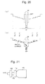
- Fig. 21 is a plan view showing a pixel structure using a normal type of embedded photodiode.
- This structure has a floating diffusion FD located on one side of the photodiode PD.
- a transfer transistor TX provided between them is turned on, photocharges flow from the photodiode PD to the floating diffusion FD and are stored therein,
- RG is a transistor for resetting the floating diffusion FD.
- the photocharges produced by the photodiode PD requires a non-negligible length of time to reach the floating diffusion PD, and a portion of the charges cannot be able to reach the floating diffusion within the predetermined short photoelectric conversion time.
- the photocharges usage efficiency will deteriorate, and the detection sensitivity will not be improved to the expected level even if the size of the light-receiving surface of the photodiode; rather, it will be a major cause of image-quality deterioration.
- the present invention has been developed in view of the aforementioned problem, and its objective is to provide a solid-state image sensor capable of efficiently using the photocharges produced by the photodiodes to improve the detection sensitivity even in a high-speed imaging operation in which the photocharge storage time available for taking one frame of image is short.
- the present invention also provides a method for producing such an image sensor.
- a solid-state image sensor aimed at solving the aforementioned problem is a solid-state image sensor having a plurality of pixels arranged thereon, which is characterized in that each of the pixels includes a photodiode for receiving light and producing photocharges, a floating region formed in the central portion of the light-receiving surface of the photodiode, and a transfer transistor having a gate surrounding the floating region.
- the solid-state image sensor it is desirable that a potential is changed from the circumferential portion of the light-receiving surface toward the central portion thereof so that the photocharges produced by the photodiode are moved toward the central portion of the light-receiving surface.
- the concentration and/or depth of an impurity injected in a substrate may be changed in an inclined form from the circumferential portion of the light-receiving surface of the photodiode to the central portion thereof.
- the concentration and/or depth of an impurity injected in a substrate may be changed in a step-like form from the circumferential portion of the light-receiving surface of the photodiode to the central portion thereof.
- the difference between the inclined form and step-like form may be unclear.
- an impurity such as phosphorus (P), arsenic (A) or boron (B)
- P phosphorus
- A arsenic
- B boron
- the impurity diffuses, whereby the corner of the impurity layer is rounded and the layer approximates to an inclined form.
- the potential change from the circumferential portion of the light-receiving surface of the photodiode to the central portion thereof is created by changing the depth of injection of an impurity ion into a substrate by using a plurality of photomasks.
- the potential is changed from the circumferential portion of the light-receiving surface of the photodiode toward the central portion thereof by changing the amount of injection of an impurity ion into a substrate by using a plurality of photomasks.
- the floating region such as a floating diffusion
- the floating region is formed substantially at the center of the light-receiving surface of the photodiode.
- This design significantly reduces the maximum distance from a given point on the light-receiving surface to the floating region as compared to case where the floating region is formed at one end of the light-receiving surface of the photodiode, so that the time required for the photocharges produced by the photodiode to reach the floating region is shortened. Therefore, even if the photocharge storage time is limited or the light-receiving surface of the photodiode is enlarged, there will be only a small amount of charges that will be discarded before reaching the floating region, i.e. that cannot be reflected in the optical signal, whereby the detection sensitivity and the S/N ratio are improved.
- the inclined or step-like potential change due to the difference in the concentration and/or depth of an impurity helps the photocharges produced by the photodiode to move from the circumference to the center of the light-receiving surface. Therefore, the photocharges easily accumulate around the transfer transistor, and when the transfer transistor is on, they will be efficiently and promptly transferred to the floating region.
- the photocharges produced by the photodiode will be efficiently collected and eventually reflected in the signal, whereby the detection sensitivity and S/N ratio are improved, so that the images obtained by high-speed imaging will have better qualifies.
- a solid-state image sensor which is an embodiment of the present invention, and a method for producing this image sensor are hereinafter described with reference to the attached drawings.
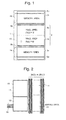
- Fig. 1 is a schematic plan view showing the layout on a semiconductor chip of the solid-state image sensor of the present embodiment
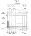
- Fig. 3 is a plan view showing a schematic configuration of the pixel area and memory area in the solid-state image sensor of the present embodiment
- Fig. 4 is a block diagram of the main portion corresponding to approximately one-half of the semiconductor chip of the solid-state image sensor of the present embodiment.
- the pixel area 2 (2a and 2b) for receiving light and producing signals for each pixel and the memory areas 3a and 3b for holding the signals for a predetermined number of frames are not intermixed but completely separated from each other on the semiconductor substrate 1 so that each area forms a definite block.
- a total of N ⁇ M pixels 10 consisting of N rows and M columns are arranged in a two-dimensional array.
- This pixel area 2 is divided into the first pixel area 2a and second pixel area 2b, each of which has (N/2) ⁇ M pixels arranged inside.
- first memory area 3a is provided across a first current source area 6a having a small area
- second memory area 3b is provided above the second pixel area 2b across a second current source 6b which also has a small area.
- the first and second memory areas 3a and 3b each include a first or second vertical scan circuit area 4a or 4b and a first or second horizontal scan circuit area 5a or 5b, each circuit area being provided with circuits such as shift resisters and decoders for controlling the reading of signals from the memory area 3a or 3b, As shown in Fig. 3 , each memory area 3a or 3b has 64 bundles of output lines SS01-SS64, including 32 bundles at each of the upper and lower ends, for reading signals to the outside of the sensor.
- the solid-state image sensor of the present embodiment is nearly symmetrical with respect to a horizontal border line extending approximately through the center of the pixels area 2 to divide this area into upper and lower sections.
- the structure and operation of the upper and lower sections are basically identical. Therefore, the following description is mainly concerned with the structure and operation of the lower section, i.e. the first pixel area 2a, first memory area 3a, first vertical scan circuit area 4a and first horizontal scan circuit area 5a.
- the number of pixels i.e. the values of N and M, can be arbitrarily determined. Increasing these values improves the image resolution but also unfavorably results in either an increase in the entire chip area or a decrease in the chip area per one pixel.
- the total number of pixels arranged in each of the first and second pixel areas 2a and 2b is 42240, i.e. 320 pixels in the horizontal direction and 132 pixels in the vertical direction, as shown in Figs. 3 and 4 .
- Fig. 2 is a schematic plan view showing the layout of one pixel 10 within the pixel area 2 (2a and 2b).
- One pixel 10 occupies roughly one square area, which is further divided into three areas, i.e. the photoelectric conversion area 11, pixel circuit area 12 and wiring area 13.
- the wiring area 13 a bundle of vertically extending (N/2)+ ⁇ pixel output lines 14 are provided.
- the value of ⁇ may be zero, in which case the number of pixel output lines passing through one wiring area 13 in the present example is 132.
- Fig. 5 is a circuit configuration diagram of one pixel 10 shown in Fig. 2 .
- the pixel 10 includes the following elements: a photodiode 31 for receiving light and producing photocharges; a transfer transistor 32, which is located near the photodiode 31, for transferring the photocharges; a floating diffusion (FD) 33, which is connected to the photodiode 31 via the transfer transistor 32, for temporarily storing the photocharges; a storage transistor 34 and storage capacitor 36 for storing charges overflowing from the photodiode 31 through the transfer transistor 32 in the process of storing photocharges; a reset transistor 35 for discharging the charges stored in the floating diffusion 33 and the storage capacitor 36; a source follower amplifier 43 with a two-stage configuration including a pair of cascade-connected PMOS transistors 37 and 38 and another pair of cascade-connected NMOS transistors 40 and 41, for extracting charges stored in the floating diffusion 33 or in both the floating diffusion 33 and the storage capacitor 36 to the outside as voltage signals (this amplifier corresponds to
- Drive lines 15 for supplying control signals ⁇ T, ⁇ C, ⁇ R and ⁇ X are respectively connected to the gate terminals of the transfer transistor 32, storage transistor 34, reset transistor 35, and selection transistors 38 and 41 of the source follower amplifier 43. As shown in Fig. 4 , these drive lines are common to all the pixels within the pixel area 2. This configuration enables simultaneous driving at all the pixels.
- the output 42 of the transistor 41 in the second stage of the source follower amplifier 43 is connected to one of the 132 pixel output lines 14 (i.e. the pixel output line denoted by numeral 141 in Fig. 5 ) provided in the aforementioned wiring area 13.
- a pixel output line 141 is provided for every pixel 10, i.e. independently for each pixel 10. Therefore, the present solid-state image sensor has as many pixel output lines as the number of pixels, i.e. 84480.
- the source follower amplifier 43 functions as a current buffer for driving the pixel output line 141 at high speeds.
- each pixel output line 141 extends from the pixel area 2a to the memory area 3a and hence acts as a considerably large capacitive load.
- Driving such an element at high speeds requires a large-sized transistor through which high currents can be passed.
- the floating diffusion 33 for converting photocharges to voltage should preferably have the smallest possible capacitance.
- the parasitic capacitance of the gate terminal of the transistor connected to the floating diffusion 33 causes an effective increase in the capacitance of the floating diffusion 33.
- this transistor 37 should preferably be a small-sized transistor with a small gate input capacitance.
- the source follower amplifier 43 in the present embodiment has a two-stage configuration, where a small-sized transistor is used as the transistor 37 in the first stage to reduce the input gate capacitance while large-sized transistors are used as the second-state transistors 40 and 41 to ensure a high output current.
- the selection transistor 38 in the first stage of the source follower amplifier 43 is not essential for the basic operation. However, when the second-stage selection transistor 41 is off, this selection transistor 38 can be simultaneously turned off to block the flow of current from the current source 39 into the transistor 37 and thereby suppress the consumption of electric power.
- Fig. 6 is a schematic plan view showing the layout of the photoelectric conversion area 11 in one pixel 10
- Fig. 7 is a schematic vertical sectional view of the photoelectric conversion area 11 and other important elements
- Fig. 8 is a schematic potential diagram at the vertical section indicated by the arrowed line A-A' in Fig. 6 .
- the photodiode 31 which has a photo-receiving surface that is substantially rectangular when viewed from above, has an embedded photodiode structure.
- the exposure time is extremely short. Therefore, to ensure appropriate exposure, the photodiode of each pixel 10 needs to have the largest possible photo-receiving surface so that it can receive the largest possible amount of incident light.
- increasing the area of the photo-receiving surface of the photodiode normally causes a problem relating to the time required for the photocharges to reach the floating diffusion, particularly for the photocharges produced in the circumferential portion of the photo-receiving surface.
- the solid-state image sensor of the present embodiment has adopted a special structure, as hereafter described, to improve the charge-transfer speed.
- the floating diffusion is normally placed next to the photodiode.
- the present solid-state image sensor has a small-sized floating diffusion 331 located nearly at the center of the photodiode 31, with the ring-shaped gate of the transfer transistor 32 encircling the floating diffusion 331
- Fig. 7 shows one example, in which a p-well region 61 having a predetermined thickness is formed on an n-type silicon semiconductor substrate (n-sub) 60, and an n-type semiconductor region 62 is formed in the p-well region 61.
- a p + -type semiconductor region 63 is formed on the surface of the n-type semiconductor region 62. This pn junction forms an embedded photodiode 31.
- n + -type semiconductor region At the center of the photodiode 31, there is a blank area of the n-type semiconductor region 62, within which an n + -type semiconductor region is formed on the surface layer of the p-well region 61.
- This n + -type region functions as the floating diffusion region 331.
- a ring-shaped gate electrode made of polysilicon or other materials is created, via an insulator film on the surface layer, to form a transfer transistor 32.
- the provision of the floating diffusion 331 at the center of the photodiode 31 almost halves the maximum moving distance of the photocharges from the circumference of the photodiode 31 to the floating diffusion 331 as compared to the case where the floating diffusion is provided next to one end of the photodiode. Accordingly, the photocharges can reach the floating diffusion 331 within a shorter period of time irrespective of where they are generated within the circumferential portion of the photodiode 31. Therefore, even in the case where the period of time assigned to the photocharge storage process is short, there will be only a small amount of photocharges that cannot reach the floating diffusion 31.
- the amount (or depth) of injection (doping) of impurities is changed in stages by using a plurality of photomasks 70a-70d differing in the layout of the shielding area 71 and passing area 72, as shown in Fig. 19 .
- an annealing process is performed to appropriately diffuse the injected impurities so that the amount (or depth) of doping (or injection) gradually increases from the circumferential portion toward the center of the photodiode 31 (i.e. toward the floating diffusion 331).
- the magnitude of the potential gradient can be determined as follow: Given that t denotes an allowable time for a photocharge to move through the photodiode 31, W denotes the maximum moving distance, ⁇ denotes the degree of mobility of the charge, and E denotes an average internal field created within the photodiode 31 by the potential gradient, the values satisfy the condition of t ⁇ W /( ⁇ E ). Due to this intended potential gradient created by a skillfully devised process, a photocharge produced by incident light at a location closer to the circumference of the photodiode 31 is more rapidly accelerated toward the center.
- the provision of the floating diffusion 331 at the center of the photodiode 31 offers the previously described significant advantages.
- the previous configuration causes the problem that the aperture ratio will decrease if another element, such as a storage capacitor 36 for storing photocharges that have overflowed, is placed close to the floating diffusion 331.
- This problem is avoided in the present embodiment by providing a second floating diffusion 332 as an n + -semiconductor region within the pixel circuit area 12 in addition to the aforementioned floating diffusion 331 which photocharges directly flow into as described previously (this floating diffusion is hereinafter called the first floating diffusion), with a wire 333 made of aluminum or other kinds of metal connecting the first floating diffusion 331 and the second floating diffusion 332 to equalize their potential.
- the first floating diffusion 331 and the second floating diffusion 332 integrally function as a floating diffusion 33 which serves as the detection node for converting electric charge signals into voltage signals.
- the potential of the photodiode 31 in the present embodiment has an inclined form.
- the photocharges produced by the photodiode 31 move toward the center while repeating the drifting and diffusing actions alternately.
- the photocharges will be efficiently transferred into the floating diffusion 331.
- each of the first and second memory areas 3a and 3b includes memory section units 20 whose number equals the number L of storage frames. These memory section units 20 are arrayed in the extending direction of the 132 pixel output lines 14 which are respectively connected to the 132 pixels 10 vertically arranged within the pixel area 2a or 2b.
- the number L of storage frames, or the number of frames for continuous imaging is 104. Accordingly, 104 pieces of memory section units 20 are vertically arranged to form a column, and 320 copies of this column are arranged horizontally.
- the second memory area 3b also has the same number of memory section units 20.
- Fig. 9 is a schematic diagram showing the internal configuration of one memory section unit 20.
- Each memory section unit 20 includes a total of 132 memory sections 22 forming an array with 12 rows and 11 columns.
- Each memory section 20 is connected to a different pixel output line 141.
- the pixel output lines 141 establish a one-to-one relation between the memory sections 22 and the pixels 10 within the pixel area 2a.
- the 132 memory sections 22 within one memory section unit 20 hold output signals received from the 132 pixels 10 forming one column within the pixel area 2a. Therefore, the 320 memory section units 20 forming one horizontal row in Fig. 4 (i.e. the row of memory section units denoted by numeral 21 in Fig.
- the present device can hold 104 frames of pixels signals.
- all outputs of the 132 memory sections 22 in each memory section unit 20 are connected together to form a single output line 23.
- the horizontally arranged memory section units 20 are divided into groups each consisting of ten neighboring memory section units 20.
- 32 groups of memory section units 20 are horizontally arranged, where the signal output lines 23 of the ten memory section units 20 in each group are connected together to form a single line.
- the signal output lines 23 of the vertically arranged 104 memory section units 20 are also connected together to form a single line.
- a memory section unit block which is a collection of the memory section units 20 sharing the same signal output line 23, is denoted by numeral 50.
- the configuration described to this point results in 32 signal output lines 23 extracted from the first memory area 3a and the same number of signal output lines 23 extracted from the second memory area 3b.
- the signals extracted through these signal output lines 23 are denoted by numerals SS01-SS64.
- Fig. 10 is a circuit diagram of one memory section 22.
- One memory section 22 has four memory units.
- Each memory element 24 (24a-24d) which serves as a minimum memory unit, is composed of a sampling transistor 26 (26a-26d) connected to one pixel output line 141, a capacitor 25 (25a-25d) connected via the sampling transistor 26 to the pixel output line 141, and a reading transistor 27 (27a-27d) for reading an analogue voltage signal held in the capacitor 25.
- One memory section 22 consists of the combination of these four memory elements 24 (24a-24d). Accordingly, each memory section 22 can hold flour different analogue voltage signals extracted from the same pixel through the same pixels output line 141.
- the signal output lines 23a, 23b, 23c and 23d via the four reading transistors 27a-27d are independent of each other. This means that the output line 23 shown in Fig. 8 actually consists of four lines, which are separately extracted for output.
- the memory elements 24a-24d can also be used in other operational modes. For example, if the storage capacitor 36 of each pixel 10 is not used, there is no need to consider the signal after an overflow and the noise signal contained in the signal after an overflow, in which case the corresponding memory elements 24 can be used to increase the number of frames for continuous imaging. As a result, the possible number of frames for continuous imaging will be doubled to 208. If the noise removal is also unnecessary, the possible number of frames for continuous imaging will be further doubled to 416.
- the capacitors 25a-25d can be created, for example, by a double polysilicon gate structure or stack structure. Using a CCD structure to hold electric charges would cause the problem that an aliasing due to dark charges caused by thermal excitation or other factors would be added to the photo signal.
- the capacitors 25a-25d in the form of a double polysilicon gate structure or stack structure cause no such dark charges and hence no addition of aliasing, thus improving the S/N ratio of the signals to be extracted to the outside.
- Fig. 11 is a block diagram showing a schematic configuration for reading signals held in the memory sections within the memory area 3a through the previously described signal output line 23.
- one memory section unit 20 is selected by a combination of the horizontal shift, registers HSR1-HSR320 and vertical shift registers VSR1-VSR104.
- the memory sections 22 are sequentially selected to extract pixel signals one after another.
- the solid-state image sensor of the present invention offers two different options for the drive mode: one drive mode is for a short photocharge storage time and the other for a relatively long photocharge storage time.
- the former mode is suitable for a photocharge storage time shorter than a range from 10 to 100 ⁇ sec, i.e. in the case where the amount of dark charges that generates in the transfer transistor 32 is negligible.
- This drive mode can be preferably used when the imaging is performed at a high rate of one million frames per second or higher.
- Fig. 12 is a drive timing chart of the operation mode for a short photocharge storage time
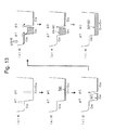
- Fig. 13 is a schematic potential diagram inside each pixel 10 during this drive mode.
- C PD , C FD and C CS denote the capacitances of the photodiode 31, floating diffusion 33 and storage capacitor 36, respectively
- C FD +C CS denotes the combined capacitance of the floating diffusion 33 and storage capacitor 36.
- the signal ⁇ X which is a common control signal supplied to every pixel 10
- the signals ⁇ T, ⁇ C and ⁇ R which are also common control signals, are set to a high level to turn on the transfer transistor 32, storage transistor 34 and reset transistor 35 (time t0), whereby the floating diffusion 33 and storage capacitor 36 are reset (or initialized).
- the photodiode 31 is completely depleted. The potential at this point in time is shown in Fig. 13(a) .
- ⁇ R is set to a low level to turn off the reset transistor 35, whereupon a noise signal N2, which equivalently contains a random noise generating in the floating diffusion 33 and storage capacitor 36 and a fixed pattern noise resulting from a variation in the threshold voltage of the transistor 37 in the source follower amplifier 43, is generated in the floating diffusion 33 (refer to Fig. 13(b) ), and an output current corresponding to this noise signal N2 flows through the pixel output line 141.
- a sampling pulse ⁇ N2 is given to the memory section 22 to turn on the sampling transistor 26d so that the noise signal N2 outputted through the pixel output line 141 is held by the capacitor 25d.
- ⁇ C is set to the low level to turn off the storage transistor 34, whereupon the signals stored in the floating diffusion 33 and storage capacitor 36 at this point in time are distributed to the floating diffusion 33 and the storage capacitor 36 according to the ratio of their capacitances C FD and C CS (refer to Fig. 13(c) ).
- a noise signal N1 which contains a random noise generated when ⁇ C was turned off and a fixed pattern noise resulting from a variation in the threshold voltage of the transistor 37 in the source follower amplifier 43, is generated in the floating diffusion 33, and an output current corresponding to this noise signal N1 flows through the pixel output line 141.
- a sampling pulse ⁇ N1 is given to the memory section 22 to turn on the sampling transistor 26c so that the noise signal N1 outputted through the pixel output line 141 is held by the capacitor 25c.
- the transfer transistor 32 Since the transfer transistor 32 is maintained in the ON state, the photocharges generated by light falling onto the photodiode 31 flow through the transfer transistor 32 (this state is shown in Fig. 8(b) ) into the floating diffusion 33, and are stored in the floating diffusion 33, being superimposed on the noise signal N1 (time 13). If the floating diffusion 33 is saturated due to a large amount of photocharges produced in the photodiode 31 by strong incident light, the overflowing charges are stored through the storage transistor 34 into the storage capacitor 36 (refer to Fig. 13(d) ). Setting the threshold voltage of the storage transistor 34 at an appropriately low level enables those charges to be efficiently transferred from the floating diffusion 33 to the storage capacitor 36.
- a sampling pulse ⁇ S1 is given to the memory section 22, with the storage transistor 34 in the OFF state, to turn on the sampling transistor 26a, whereby a signal corresponding to the charge stored in the floating diffusion 33 at that point in time (time t4) is extracted through the pixel output line 141 and held in the capacitor 25a (refer to Fig. 13(e) ).
- the signal stored in the floating diffusion 33 at this point in time results from the superposition of a noise signal N1 and a signal S1 corresponding to the charge before an overflow. Accordingly, the signal held in the capacitor 25a equals S1+N1, which does not reflect the amount of charge stored in the storage capacitor 36.
- ⁇ C is set to the high level to turn on the storage transistor 34, whereupon the charge held in the floating diffusion 33 at that point in time is mixed with the charge held in the storage capacitor 36 (refer to Fig. 13(f) ).
- a sampling pulse ⁇ S2 is given to the memory section 22 to turn on the sampling transistor 26b (time t5), whereby a signal corresponding to the charges held in the floating diffusion 33 and the storage capacitor 36, i.e. a signal resulting from the superposition of the noise signal N2 and the signal S2 corresponding to the charge after the overflow, is extracted through the pixel output line 141 and held in the capacitor 25b.
- the signal to be held in the capacitor 25b is S2+N2, which reflects the amount of charge stored in the storage capacitor 36.
- the signals S1+N1, S2+N2, N1 and N2 are respectively held in the four capacitors 25a, 25b, 25c and 25d included in one memory section 22.
- the noise signals N1 and N2 containing the random noise and fixed pattern noise are obtained separately from the other signals containing these noise signals.
- These signals can be respectively read from the capacitors 25a, 25b, 25c and 25d and then subjected to a subtracting operation to obtain high S/N image signals free from the influence of the noise signals N1 and N2. Since the charges that have overflowed from the floating diffusion 33 are not discarded but utilized, even a strong incident light barely causes saturation, so that the resultant signal can reflect the light. Thus, a wide dynamic range is ensured.
- the possibilities of widening the dynamic range in this manner are described in detail in the Japanese Unexamined Patent Application Publication No. 2006-245522 and other documents. Therefore, no explanation will be made in this specification.
- Fig. 14 is a drive timing chart in the case where the photocharge storage time is relatively long
- Fig. 15 is a schematic potential diagram inside the pixel in this operation.
- the transfer transistor 32 is turned off during the photocharge storage period so that the photocharges produced in the photodiode 31 will be stored in a depletion layer; the transfer transistor 32 is turned off during the photocharge storage period; and the sampling of the noise signal N1 is performed at the end of the photocharge storage period so that the dark charges (and photocharges) that generate in the floating diffusion 33 will not be included in the signal S1.
- the purpose of turning off the transfer transistor 32 is to create an accumulation state at the interface between the silicon and insulating film immediately below its gate, thus filling the silicon surface with holes to prevent intrusion of dark charges through the interface between the silicon and insulating film.
- Another difference is that, taking into account the long photocharge storage time, the selection transistors 38 and 41 of the source follower amplifier 43 are turned off for a predetermined period of time to reduce the power consumption.
- ⁇ T, ⁇ C and ⁇ R are set to high levels to turn on both the storage transistor 34 and reset transistor 35 (time t10), whereby the floating diffusion 33 and storage capacitor 36 are reset (or initialized).
- time t10 the storage transistor 34 and reset transistor 35
- the floating diffusion 33 and storage capacitor 36 are reset (or initialized).
- the photodiode 31 is completely depleted.
- the state of potential at this point in time is shown in Fig. 15(a) .
- ⁇ R is set to the low level to turn off the reset transistor 35, whereupon a noise signal N2, which equivalently contains a random noise generating in the floating diffusion 33 and the storage capacitor 36 and a fixed pattern noise resulting from a variation in the threshold voltage of the transistor 37 in the source follower amplifier 43, is generated in the floating diffusion 33 (refer to Fig. 15(b) ), and an output current corresponding to this noise signal N2 flows through the pixel output line 141.
- a sampling pulse ⁇ N2 is given to the memory section 22 to turn on the sampling transistor 26d, whereby the noise signal N2 is extracted through the pixel output line 141 and held in the capacitor 25d.
- ⁇ C is set to the low level to turn off the storage transistor 34, whereupon the signal chargess stored in the floating diffusion 33 and storage capacitor 36 at this point in time are distributed to the floating diffusion 33 and storage capacitor 36 according to the ratio of their capacitances C FD and C CS .
- ⁇ T is set to the low level to turn off the transfer transistor 32
- ⁇ X is also set to the low level to turn off the two selection transistors 38 and 41 of the source follower amplifier 43 (time t12).
- a potential barrier is formed between the photodiode 31 and the floating diffusion 33, creating a condition where photocharges can be stored in the photodiode 31 (refer to Fig. 15(c) ).
- the photocharges produced by incident light falling onto the photodiode 31 are stored in the capacitance C PD of the photodiode 31.
- C PD capacitance of the photodiode 31.
- excessive charges flow through the transfer transistor 32, to be stored in the floating diffusion 33 and superimposed on the noise signal that has been distributed as described previously. If the floating diffusion 33 is saturated by stronger incident light, the charges will be stored through the storage transistor 34 into the storage capacitor 36 (refer to Fig. 15(d) ).
- ⁇ X is set to the high level to turn on the selection transistors 38 and 41, after which a sampling pulse ⁇ N1 is given to the memory section 22 to turn on the sampling transistor 26c, whereby a noise signal N1 corresponding to the signal charge stored in the floating diffusion 33 at this point in time (time t13) is extracted through the pixel output line 14 and held in the capacitor 25c.
- the noise signal N1 at this point in time contains a fixed pattern noise due to a variation in the threshold voltage of the transistor 37 in the source follower amplifier 43.
- ⁇ T is set to the high level to turn on the transfer transistor 32, whereupon the photocharges stored in the photodiode 31 are completely transferred to the floating diffusion 33 (refer to Fig. 15(e) ).
- a sampling pulse ⁇ S1 is given to the memory section 22 to turn on the sampling transistor 26a, whereby a signal corresponding to the charge stored in the floating diffusion 33 is extracted through the pixel output line 14 and held in the capacitor 25a.
- This signal results from the superposition of the aforementioned noise signal N1 and the signal corresponding to the charge stored in the photodiode 31, i.e. the signal S1 before the overflow, and hence equals S1+N1.
- ⁇ C is set to the high level to turn on the storage transistor 34, whereupon the charge held in the floating diffusion 33 at that point in time is mixed with the charge held in the storage capacitor 36 (refer to Fig. 15(f) ).
- a sampling pulse ⁇ S2 is given to the memory section 22 to turn on the sampling transistor 26b (time t15), whereby a signal corresponding to the charges held in the floating diffusion 33 and storage capacitor 36 are extracted through the pixel output line 141 and held in the capacitor 25b. This signal equals S2+N2.
- the signals S1+N1, S2+N2, N1 and N2 are respectively held in the four capacitors 25a, 25b, 25c and 25d included in one memory section 22.
- the noise signals N1 and N2 containing the random noise and fixed pattern noise are obtained separately from the other signals containing these noise signals.
- These signals can be respectively read from the capacitors 25a, 25b, 25c and 25d and then subjected to subtraction to obtain high S/N image signals free from the influence of the noise signals N1 and N2. Since the charges that have overflowed from the floating diffusion 33 are not discarded but utilized, even a strong incident light barely causes saturation, so that the resultant signal can reflect the light. Thus, a wide dynamic range is ensured.
- the control signals ⁇ X, ⁇ T, ⁇ R and ⁇ C supplied to each pixel 10 are common to all the pixels. Therefore, the aforementioned operations of storing photocharges and transferring signals from each pixel 10 to the memory section 22 are simultaneously performed at all the pixels 10. That is, by one cycle of these operations, one frame of image signals are held in the 320 memory sections 22 horizontally arranged in the memory area a shown in Fig. 3 . The operations are repeated 104 cycles to store the image signals in the memory sections 22 in all the memory section units 20. In the 105 th and subsequent cycles, the operation of writing signals in the memory sections 22 is once more initiated from the topmost memory section units 20. This, the signal-holding operation is cyclically carried out. This process is continued, for example, until a command signal for discontinuing the imaging is externally given. When the command signal for discontinuing the imaging is given and the imaging is thereby discontinued, the latest 104 frames of image signals are held in the memory areas 3a and 3b.
- a transistor for resetting is connected to each pixel output line 141.
- the sampling transistor 26 of the memory section 22 is turned on and, simultaneously, the transistor for resetting connected to the corresponding pixel output line 141 is turned on, whereby the signal stored in the capacitor 25 is reset through the sampling transistor 26 and the pixel output line 141. After this resetting operation is performed, a new signal is held in the capacitor 25.
- the signals held in the capacitors 25 of each memory section 22 are read by sequentially turning on the reading transistors 27 connected to the same signal output line 23. Since the four reading transistors 27a-27d of the same memory section 22 are respectively connected to the different signal output lines 23a-23d, the signals held in each of the four capacitors 25a-25d in the same memory section 22 can be simultaneously read. Using these signals, the subtracting operations of (S1+N1)-N1 and (S2+N2)-N2 can be performed by a subtraction circuit (now shown) provided inside or outside the sensor to extract each of the signals S1 and S2 free from the random noise and fixed pattern noise.
- Which of S1 and S2 should be used is determined with reference to an appropriate signal level (threshold value) equal to or lower than the saturation level of the signal S1; S1 is selected when the signal is equal to or higher than the reference level, and S2 when the signal is lower than the reference level. By performing this selection below the signal saturation level, it is possible to avoid the influence of saturation variation of the signal S1.
- Fig. 16 is an operation timing chart of sequential reading of the signals from the memory areas 3a and 3b
- Fig. 17 is an operation timing chart of the main portion of the horizontal shift registers HSR
- Fig. 18 an operation timing chart of the main portion of the vertical shift registers VSR.
- the reading order at the leftmost memory section unit block 50 in the 320 memory section units 20 corresponding to the first frame in Fig. 11 is hereinafter described.
- image signals of eleven pixels are sequentially read from the memory sections 22 in the left-to-right direction of the first horizontal row shown in Fig. 9 .
- This memory section unit 20-01 is selected by activating the horizontal shift register HSR1 and vertical shift register VSH1.
- the horizontal reading clock H-CLK produces a moving pulse signal that turns on the reading transistors 27 of the memory sections 22, one by one, from left to right in the horizontal direction.
- the signals y1, y2 and y3 in Fig. 17 are one example of this pulse signal.
- a clock V-CLK for shifting the vertical reading position is supplied, whereby the memory sections 22 in the next (second) row are selected. Then, these memory sections 22 are similarly selected, from left to right, for the reading of eleven pixels. Such a process of reading pixel signals is repeated until the end of the twelfth row.
- the signals v1, v2 and v3 shown in Fig. 18 are one example of the signal for activating the reading transistor 27 corresponding to each row in the vertical direction.
- the horizontal shift register HSR2 and vertical shift register VSR1 are activated to select the memory section unit 20-02 on the right, and this memory section unit 20-02 becomes the target of reading, as shown in Fig 16 .
- the signals are read by turning on the reading transistors 27 of each memory section 22, for one pixel after another, in the order of row ⁇ column.
- the sequential selection of each memory section unit 20 is continued until the memory section unlit 20-10.
- the reading process for one frame is completed.
- the other memory section unit blocks 50 the operation of reading signals from the memory sections of the corresponding memory section units is similarly performed.
- the reading of pixel signals of the second frame is subsequently initiated. That is, the horizontal shift register HSR1 and the vertical shift register VSR2 are activated to select the leftmost memory section unit of the second row shown in Fig. 11 , and the reading operation is performed in the same order as in the case of the first frame. This process is repeated to perform the reading operation through the end of the 104 th frame. It should be noted that the reading process is not specifically limited to this one; it can be appropriately modified.
- the solid-state image sensor of the present embodiment can rapidly and efficiently transfer photocharges to the floating diffusion 33 while allowing the use of a large-sized photodiode 31 to receive a larger amount of light. Therefore, even if, as in the case of a continuous high-speed imaging operation, the exposure time per one frame is short, the detection sensitivity and S/N ratio will be improved, so that the resultant images will have better qualities.
Landscapes
- Engineering & Computer Science (AREA)
- Multimedia (AREA)
- Signal Processing (AREA)
- Solid State Image Pick-Up Elements (AREA)
- Transforming Light Signals Into Electric Signals (AREA)
Abstract
Description
- The present invention relates to a solid-state image sensor and a method for producing this sensor. More specifically, it relates to a solid-state image sensor capable of high-speed operations suitable for taking images of high-speed phenomena such as destructions, explosions and combustions, and a method for producing such a sensor.
- High-speed imaging devices (high-speed video cameras) for taking consecutive images of high-speed phenomena such as explosions, destructions, combustion, collisions and discharges for only a short period of time have been conventionally developed (for example, refer to Non-Patent
Document 1 and other documents). Such high-speed imaging devices need to perform an ultrahigh-speed imaging operation that exceeds a level of approximately one million frames per second. Accordingly, they use solid-state image sensors capable of high-speed operations, which have special structures different from those of the imaging devices conventionally used in normal video cameras, digital cameras and similar devices. - One example of this type of solid-state image sensor is disclosed in Patent Document I and other documents, which is referred to as an in-situ storage image sensor (IS-CCD). An outlive of this image sensor is as follows: A storage CCD, which also serves for the transfer of a specified number of recorded images (frames), is provided for each photodiode as a photo-receiver. During an imaging operation, pixel signals resulting from photoelectric conversion by the photodiode are sequentially transferred to the storage CCD. After the imaging operation is completed, the pixel signals corresponding to the specified number of record frames stored in the storage COD are collectively read, and the images corresponding to the specified number of record frames are reproduced outside the image sensor. During the imaging operation, pixel signals exceeding the specified number of image frames are discarded from the oldest ones. Thus, the latest set of pixel signals corresponding to the specified number of frames are held in the storage CCD. This means that, when the transfer of pixel signals to the storage CCD is suspended at the completion of the imaging operation, one can obtain the latest series of images ranging from the completion of the imaging operation back through a period of time corresponding to the specified number of record frames.
- In such a high-speed imaging operation, the period of time in which the photodiodes are exposed to light to obtain one frame of pixel signals is extremely short as compared to the normal imaging operation. For example, in the case of a high-speed imaging operation at one million frames per second, the exposure time for one frame of image is equal to or shorter than 1 µsec. Therefore, to ensure an adequate detection sensitivity, it is necessary to receive the largest possible amount of light by the photodiode in each pixel. Accordingly, it is desirable to provide the photodiode with the largest possible light-receiving surface. However, increasing the size of the light-receiving surface of the photodiode causes the following problem.
-
Fig. 21 is a plan view showing a pixel structure using a normal type of embedded photodiode. This structure has a floating diffusion FD located on one side of the photodiode PD. When a transfer transistor TX provided between them is turned on, photocharges flow from the photodiode PD to the floating diffusion FD and are stored therein, RG is a transistor for resetting the floating diffusion FD. - In this structure, when the size of the light-receiving surface of the photodiode is increased, the photocharges produced by the photodiode PD requires a non-negligible length of time to reach the floating diffusion PD, and a portion of the charges cannot be able to reach the floating diffusion within the predetermined short photoelectric conversion time. As a result, the photocharges usage efficiency will deteriorate, and the detection sensitivity will not be improved to the expected level even if the size of the light-receiving surface of the photodiode; rather, it will be a major cause of image-quality deterioration.
-
- Patent Document 1: Japanese Unexamined Patent Application Publication No.
2001-345441 - Non-Patent Document 1: Kondo et al., "Kousokudo Bideo Kamera HyperVision HPV-1 no Kaihatsu (Development of "HyperVision HPV-1" High-Speed Video Camera)", Shimadzu Hyouron (Shimadzu Review), Shimadzu Hyouron Henshuu-bu, September 30, 2005, Vol. 62, No. 1/2, pp. 79-86
- The present invention has been developed in view of the aforementioned problem, and its objective is to provide a solid-state image sensor capable of efficiently using the photocharges produced by the photodiodes to improve the detection sensitivity even in a high-speed imaging operation in which the photocharge storage time available for taking one frame of image is short. The present invention also provides a method for producing such an image sensor.
- A solid-state image sensor according to the present invention aimed at solving the aforementioned problem is a solid-state image sensor having a plurality of pixels arranged thereon, which is characterized in that each of the pixels includes a photodiode for receiving light and producing photocharges, a floating region formed in the central portion of the light-receiving surface of the photodiode, and a transfer transistor having a gate surrounding the floating region.
- In the solid-state image sensor according to the present invention, it is desirable that a potential is changed from the circumferential portion of the light-receiving surface toward the central portion thereof so that the photocharges produced by the photodiode are moved toward the central portion of the light-receiving surface.
- As a variation of the solid-state image sensor according to the present invention, the concentration and/or depth of an impurity injected in a substrate may be changed in an inclined form from the circumferential portion of the light-receiving surface of the photodiode to the central portion thereof.
- As another variation of the solid-state image sensor according to the present invention, the concentration and/or depth of an impurity injected in a substrate may be changed in a step-like form from the circumferential portion of the light-receiving surface of the photodiode to the central portion thereof.
- In practice, the difference between the inclined form and step-like form may be unclear. For example, in the case where an impurity, such as phosphorus (P), arsenic (A) or boron (B), is introduced into a base (e.g. a p-well) laminated to a semiconductor substrate by ion injection or other methods, when an annealing process using heat or the like is performed after a step-like change in the concentration and/or depth of the impurity is created, the impurity diffuses, whereby the corner of the impurity layer is rounded and the layer approximates to an inclined form.
- In one variation of the method for producing the solid-state image sensor according to the present invention, the potential change from the circumferential portion of the light-receiving surface of the photodiode to the central portion thereof is created by changing the depth of injection of an impurity ion into a substrate by using a plurality of photomasks.
- In another variation of the method for producing the solid-state image sensor according to the present invention, the potential is changed from the circumferential portion of the light-receiving surface of the photodiode toward the central portion thereof by changing the amount of injection of an impurity ion into a substrate by using a plurality of photomasks.
- In the solid-state image sensor according to the present invention, the floating region, such as a floating diffusion, is formed substantially at the center of the light-receiving surface of the photodiode. This design significantly reduces the maximum distance from a given point on the light-receiving surface to the floating region as compared to case where the floating region is formed at one end of the light-receiving surface of the photodiode, so that the time required for the photocharges produced by the photodiode to reach the floating region is shortened. Therefore, even if the photocharge storage time is limited or the light-receiving surface of the photodiode is enlarged, there will be only a small amount of charges that will be discarded before reaching the floating region, i.e. that cannot be reflected in the optical signal, whereby the detection sensitivity and the S/N ratio are improved.
- In the case where the potential is changed from the circumferential portion to the central portion of the light-receiving surface, the inclined or step-like potential change due to the difference in the concentration and/or depth of an impurity helps the photocharges produced by the photodiode to move from the circumference to the center of the light-receiving surface. Therefore, the photocharges easily accumulate around the transfer transistor, and when the transfer transistor is on, they will be efficiently and promptly transferred to the floating region. Thus, even in the case where the light-receiving surface of the photocharge is large-sized and the photocharge storage time is short, the photocharges produced by the photodiode will be efficiently collected and eventually reflected in the signal, whereby the detection sensitivity and S/N ratio are improved, so that the images obtained by high-speed imaging will have better qualifies.
-
-
Fig. 1 is a schematic plan view showing the layout on a semiconductor chip of a solid-state image sensor which is an embodiment of the present invention. -
Fig. 2 is a schematic plan view showing the layout of one pixel within a pixel area in the solid-state image sensor of the present embodiment. -
Fig. 3 is a plan view showing a schematic configuration of the pixel area and memory area in the solid-state image sensor of the present embodiment. -
Fig. 4 is a block diagram of the main portion corresponding to approximately one half of the semiconductor chip of the solid-state image sensor of the present embodiment. -
Fig. 5 is a circuit configuration diagram of one pixel in the solid-state image sensor of the present embodiment. -
Fig. 6 is a schematic plan view showing the layout of a photoelectric conversion area in one pixel in the solid-state image sensor of the present embodiment. -
Fig. 7 is a schematic vertical sectional view of the photoelectric conversion area and other important elements in the solid-state image sensor of the present embodiment. -
Fig. 8 is a schematic potential diagram at the vertical section indicated by the arrowed line A-A' inFig. 6 . -
Fig. 9 is a schematic configuration diagram of one memory section unit corresponding to 132 pixels vertically arranged in the solid-state image sensor of the present embodiment. -
Fig. 10 is a circuit configuration diagram of one memory section in the solid-state image sensor of the present embodiment. -
Fig. 11 is a block diagram showing a schematic configuration for reading signals held in the memory sections through output lines in the solid-state image sensor of the present embodiment. -
Fig. 12 is a timing chart of an operation mode of the solid-state image sensor of the present embodiment in the case where the photocharge storage time is short. -
Fig. 13 is a schematic potential diagram inside each pixel during the operation shown inFig. 12 . -
Fig. 14 is a timing chart of an operation mode of the solid-state image sensor of the present embodiment in the case where the photocharge storage time is relatively long. -
Fig. 15 is a schematic potential diagram inside a pixel during the operation shown inFig. 14 . -
Fig. 16 is an operation timing chart of an operation of sequentially reading pixel signals in the solid-state image sensor of the present embodiment. -
Fig. 17 is an operation timing chart of the main portion of the horizontal shift registers in the solid-state image sensor of the present embodiment. -
Fig. 18 is an operation timing chart of the main portion of the vertical shift registers in the solid-state image sensor of the present embodiment. -
Fig. 19 is a schematic diagram of the photomasks used in the process of creating a photodiode in the solid-state image sensor of the present embodiment. -
Fig. 20 is a schematic potential diagram of the photodiode in a solid-state image sensor according to another embodiment of the present invention. -
Fig. 21 is a plan view showing a pixel structure using a normal type of embedded photodiode. -
- 1 Semiconductor Substrate
- 2, 2a, 2b Pixel Area
- 10 Pixel
- 11 Photoelectric Conversion Area
- 12 Pixel Circuit Area
- 13 Wiring Area
- 14, 141 Pixel Output Line
- 15 Drive Line
- 31 Photodiode
- 32 Transfer Transistor
- 33,331, 332 Floating Diffusion
- 333 metallic Wiring
- 34 Storage Transistor
- 35 Reset Transistor
- 36 Storage Capacitor
- 37, 40Transistor
- 38, 41 Selection Transistor
- 39 Current Source
- 43 Source Follower Amplifier
- 60 n-type silicon semiconductor substrate
- 61 p-well region
- 62 n-type semiconductor region
- 63 p+-type semiconductor region
- A solid-state image sensor, which is an embodiment of the present invention, and a method for producing this image sensor are hereinafter described with reference to the attached drawings.
- An overall configuration and structure of the solid-state image sensor according to the present embodiment is initially described.
Fig. 1 is a schematic plan view showing the layout on a semiconductor chip of the solid-state image sensor of the present embodiment,Fig. 3 is a plan view showing a schematic configuration of the pixel area and memory area in the solid-state image sensor of the present embodiment, andFig. 4 is a block diagram of the main portion corresponding to approximately one-half of the semiconductor chip of the solid-state image sensor of the present embodiment. - As shown in
Fig. 1 , in the present solid-state image sensor, the pixel area 2 (2a and 2b) for receiving light and producing signals for each pixel and thememory areas semiconductor substrate 1 so that each area forms a definite block. Within therectangular pixel area 2, a total of N×M pixels 10 consisting of N rows and M columns are arranged in a two-dimensional array. Thispixel area 2 is divided into thefirst pixel area 2a andsecond pixel area 2b, each of which has (N/2)×M pixels arranged inside. - Below the
first pixel area 2a, afirst memory area 3a is provided across a firstcurrent source area 6a having a small area, while asecond memory area 3b is provided above thesecond pixel area 2b across a secondcurrent source 6b which also has a small area. The first andsecond memory areas scan circuit area scan circuit area memory area Fig. 3 , eachmemory area - The solid-state image sensor of the present embodiment is nearly symmetrical with respect to a horizontal border line extending approximately through the center of the
pixels area 2 to divide this area into upper and lower sections. The structure and operation of the upper and lower sections are basically identical. Therefore, the following description is mainly concerned with the structure and operation of the lower section, i.e. thefirst pixel area 2a,first memory area 3a, first verticalscan circuit area 4a and first horizontalscan circuit area 5a. - The number of pixels, i.e. the values of N and M, can be arbitrarily determined. Increasing these values improves the image resolution but also unfavorably results in either an increase in the entire chip area or a decrease in the chip area per one pixel. In the present example, N=264 and M=320. Accordingly, the total number of pixels arranged in each of the first and
second pixel areas Figs. 3 and4 . -
Fig. 2 is a schematic plan view showing the layout of onepixel 10 within the pixel area 2 (2a and 2b). Onepixel 10 occupies roughly one square area, which is further divided into three areas, i.e. thephotoelectric conversion area 11,pixel circuit area 12 andwiring area 13. In thewiring area 13, a bundle of vertically extending (N/2)+αpixel output lines 14 are provided. The value of α may be zero, in which case the number of pixel output lines passing through onewiring area 13 in the present example is 132. However, when a large number of wirings (e.g. aluminum wirings or other kinds of metal wirings) parallel to each other are created, the width of the wires on both ends as well as their parasitic capacitances normally tend to be different. To address these problems, a dummy wire is additionally provided at each end of the 132 pixel output lines which are used to actually pass the signals. In this case, α=2, so that the number of wires passing through onewiring area 13 is 134. -
Fig. 5 is a circuit configuration diagram of onepixel 10 shown inFig. 2 . Thepixel 10 includes the following elements: aphotodiode 31 for receiving light and producing photocharges; atransfer transistor 32, which is located near thephotodiode 31, for transferring the photocharges; a floating diffusion (FD) 33, which is connected to thephotodiode 31 via thetransfer transistor 32, for temporarily storing the photocharges; astorage transistor 34 andstorage capacitor 36 for storing charges overflowing from thephotodiode 31 through thetransfer transistor 32 in the process of storing photocharges; areset transistor 35 for discharging the charges stored in the floatingdiffusion 33 and thestorage capacitor 36; asource follower amplifier 43 with a two-stage configuration including a pair of cascade-connectedPMOS transistors NMOS transistors diffusion 33 or in both the floatingdiffusion 33 and thestorage capacitor 36 to the outside as voltage signals (this amplifier corresponds to the buffer element in the present invention); and acurrent source 39, which consists of a constant-current transistor and other components, for supplying current to thetransistors source follower amplifier 43. - Drive
lines 15 for supplying control signals ϕT, ϕC, ϕR and ϕX are respectively connected to the gate terminals of thetransfer transistor 32,storage transistor 34, resettransistor 35, andselection transistors source follower amplifier 43. As shown inFig. 4 , these drive lines are common to all the pixels within thepixel area 2. This configuration enables simultaneous driving at all the pixels. - The
output 42 of thetransistor 41 in the second stage of thesource follower amplifier 43 is connected to one of the 132 pixel output lines 14 (i.e. the pixel output line denoted by numeral 141 inFig. 5 ) provided in theaforementioned wiring area 13. Such apixel output line 141 is provided for everypixel 10, i.e. independently for eachpixel 10. Therefore, the present solid-state image sensor has as many pixel output lines as the number of pixels, i.e. 84480. - The
source follower amplifier 43 functions as a current buffer for driving thepixel output line 141 at high speeds. As shown inFig. 4 , eachpixel output line 141 extends from thepixel area 2a to thememory area 3a and hence acts as a considerably large capacitive load. Driving such an element at high speeds requires a large-sized transistor through which high currents can be passed. However, in order to raise the photoelectric conversion gain in eachpixel 10, the floatingdiffusion 33 for converting photocharges to voltage should preferably have the smallest possible capacitance. The parasitic capacitance of the gate terminal of the transistor connected to the floatingdiffusion 33 causes an effective increase in the capacitance of the floatingdiffusion 33. Therefore, for the aforementioned reason, thistransistor 37 should preferably be a small-sized transistor with a small gate input capacitance. To fulfill both the supply of high current on the output side and the low capacitance on the input side, thesource follower amplifier 43 in the present embodiment has a two-stage configuration, where a small-sized transistor is used as thetransistor 37 in the first stage to reduce the input gate capacitance while large-sized transistors are used as the second-state transistors - The
selection transistor 38 in the first stage of thesource follower amplifier 43 is not essential for the basic operation. However, when the second-stage selection transistor 41 is off, thisselection transistor 38 can be simultaneously turned off to block the flow of current from thecurrent source 39 into thetransistor 37 and thereby suppress the consumption of electric power. -
Fig. 6 is a schematic plan view showing the layout of thephotoelectric conversion area 11 in onepixel 10,Fig. 7 is a schematic vertical sectional view of thephotoelectric conversion area 11 and other important elements, andFig. 8 is a schematic potential diagram at the vertical section indicated by the arrowed line A-A' inFig. 6 . - The
photodiode 31, which has a photo-receiving surface that is substantially rectangular when viewed from above, has an embedded photodiode structure. In high-speed imaging, the exposure time is extremely short. Therefore, to ensure appropriate exposure, the photodiode of eachpixel 10 needs to have the largest possible photo-receiving surface so that it can receive the largest possible amount of incident light. However, increasing the area of the photo-receiving surface of the photodiode normally causes a problem relating to the time required for the photocharges to reach the floating diffusion, particularly for the photocharges produced in the circumferential portion of the photo-receiving surface. This problem can result in a situation where the photocharges that cannot be transferred during the short cyclic period of the high-speed imaging are eventually wasted or cause afterimages. To address these problems, the solid-state image sensor of the present embodiment has adopted a special structure, as hereafter described, to improve the charge-transfer speed. - As already stated, the floating diffusion is normally placed next to the photodiode. However, as shown in
Fig. 6 , the present solid-state image sensor has a small-sized floatingdiffusion 331 located nearly at the center of thephotodiode 31, with the ring-shaped gate of thetransfer transistor 32 encircling the floatingdiffusion 331Fig. 7 shows one example, in which a p-well region 61 having a predetermined thickness is formed on an n-type silicon semiconductor substrate (n-sub) 60, and an n-type semiconductor region 62 is formed in the p-well region 61. A p+-type semiconductor region 63 is formed on the surface of the n-type semiconductor region 62. This pn junction forms an embeddedphotodiode 31. - At the center of the
photodiode 31, there is a blank area of the n-type semiconductor region 62, within which an n+-type semiconductor region is formed on the surface layer of the p-well region 61. This n+-type region functions as the floatingdiffusion region 331. Between the floatingdiffusion region 331 formed by the n+-type semiconductor region and the surrounding n-type semiconductor region 62, a ring-shaped gate electrode made of polysilicon or other materials is created, via an insulator film on the surface layer, to form atransfer transistor 32. The provision of the floatingdiffusion 331 at the center of thephotodiode 31 almost halves the maximum moving distance of the photocharges from the circumference of thephotodiode 31 to the floatingdiffusion 331 as compared to the case where the floating diffusion is provided next to one end of the photodiode. Accordingly, the photocharges can reach the floatingdiffusion 331 within a shorter period of time irrespective of where they are generated within the circumferential portion of thephotodiode 31. Therefore, even in the case where the period of time assigned to the photocharge storage process is short, there will be only a small amount of photocharges that cannot reach the floatingdiffusion 31. - In the process of forming the p+-
type semiconductor region 61, n-type semiconductor region 62 or p-well region 61, the amount (or depth) of injection (doping) of impurities is changed in stages by using a plurality ofphotomasks 70a-70d differing in the layout of the shieldingarea 71 and passingarea 72, as shown inFig. 19 . Subsequently, an annealing process is performed to appropriately diffuse the injected impurities so that the amount (or depth) of doping (or injection) gradually increases from the circumferential portion toward the center of the photodiode 31 (i.e. toward the floating diffusion 331). Therefore, when an appropriate bias voltage is applied to the pn junction of thephotodiode 31, a potential gradient that is inclined downwards from the circumferential portion to the center of thephotodiode 31 is created, as shown inFig. 8(a) , - The magnitude of the potential gradient can be determined as follow: Given that t denotes an allowable time for a photocharge to move through the
photodiode 31, W denotes the maximum moving distance, µ denotes the degree of mobility of the charge, and E denotes an average internal field created within thephotodiode 31 by the potential gradient, the values satisfy the condition of t≤W/(µ·E). Due to this intended potential gradient created by a skillfully devised process, a photocharge produced by incident light at a location closer to the circumference of thephotodiode 31 is more rapidly accelerated toward the center. - In this process, when the
transfer transistor 32 is off, the photocharges are collected around the potential barrier formed immediately below the ring-shaped gate electrode of thetransfer transistor 32, as shown inFig. 8(a) . Then, when thetransfer transistor 32 is turned on, the collected photocharges will immediately fall into the floatingdiffusion 331 through thetransfer transistor 32, as shown inFig. 8(b) . On the other hand, if thetransfer transistor 32 is maintained in the ON state while the light is being received, the photocharges that have gathered at the center along the potential gradient will directly fall into the floatingdiffusion 331 through thetransfer transistor 32. In any of these cases, the photocharges produced by thephotodiode 31 are promptly, and with high probability, transferred to the floatingdiffusion 331. - The provision of the floating
diffusion 331 at the center of thephotodiode 31 offers the previously described significant advantages. However, the previous configuration causes the problem that the aperture ratio will decrease if another element, such as astorage capacitor 36 for storing photocharges that have overflowed, is placed close to the floatingdiffusion 331. This problem is avoided in the present embodiment by providing a second floatingdiffusion 332 as an n+-semiconductor region within thepixel circuit area 12 in addition to the aforementioned floatingdiffusion 331 which photocharges directly flow into as described previously (this floating diffusion is hereinafter called the first floating diffusion), with awire 333 made of aluminum or other kinds of metal connecting the first floatingdiffusion 331 and the second floatingdiffusion 332 to equalize their potential. This means that the first floatingdiffusion 331 and the second floatingdiffusion 332 integrally function as a floatingdiffusion 33 which serves as the detection node for converting electric charge signals into voltage signals. - As stated earlier, the potential of the
photodiode 31 in the present embodiment has an inclined form. Alternatively, it is possible to create a step-like potential, for example as shown inFig. 20 . In this case, the photocharges produced by thephotodiode 31 move toward the center while repeating the drifting and diffusing actions alternately. Thus, the photocharges will be efficiently transferred into the floatingdiffusion 331. - The internal configuration of the first and
second memory areas Fig. 4 , each of the first andsecond memory areas memory section units 20 whose number equals the number L of storage frames. Thesememory section units 20 are arrayed in the extending direction of the 132pixel output lines 14 which are respectively connected to the 132pixels 10 vertically arranged within thepixel area memory section units 20 are vertically arranged to form a column, and 320 copies of this column are arranged horizontally. Thus, thefirst memory area 3a has 104×320=33280 pieces ofmemory section units 20 arranged inside. Thesecond memory area 3b also has the same number ofmemory section units 20. -
Fig. 9 is a schematic diagram showing the internal configuration of onememory section unit 20. Eachmemory section unit 20 includes a total of 132memory sections 22 forming an array with 12 rows and 11 columns. Eachmemory section 20 is connected to a differentpixel output line 141. Thepixel output lines 141 establish a one-to-one relation between thememory sections 22 and thepixels 10 within thepixel area 2a. The 132memory sections 22 within onememory section unit 20 hold output signals received from the 132pixels 10 forming one column within thepixel area 2a. Therefore, the 320memory section units 20 forming one horizontal row inFig. 4 (i.e. the row of memory section units denoted by numeral 21 inFig. 4 ) hold the pixel signals of the lower half of one frame consisting of 320×132 pixels. Similarly, in thesecond memory area 3b located above inFig. 3 , the pixel signals of the upper half of one frame consisting of 320×132 pixels are held by 320memory section units 20 forming one horizontal row. Combining those two sets of signals produces one frame of image. With the vertically arranged 104 rows of memory section units, the present device can hold 104 frames of pixels signals. - As shown in
Fig. 9 , all outputs of the 132memory sections 22 in eachmemory section unit 20 are connected together to form asingle output line 23. Furthermore, as shown inFig. 4 , the horizontally arrangedmemory section units 20 are divided into groups each consisting of ten neighboringmemory section units 20. Thus, 32 groups ofmemory section units 20 are horizontally arranged, where thesignal output lines 23 of the tenmemory section units 20 in each group are connected together to form a single line. Thesignal output lines 23 of the vertically arranged 104memory section units 20 are also connected together to form a single line. As a result, the outputs of 1040memory section units 20 arrayed in 10 columns and 104 rows, or the outputs of 137280memory sections 22 included in thosememory section units 20, are connected together to form onesignal output line 23 in thememory area 3a. InFig. 3 , a memory section unit block, which is a collection of thememory section units 20 sharing the samesignal output line 23, is denoted bynumeral 50. The configuration described to this point results in 32signal output lines 23 extracted from thefirst memory area 3a and the same number ofsignal output lines 23 extracted from thesecond memory area 3b. The signals extracted through thesesignal output lines 23 are denoted by numerals SS01-SS64. -
Fig. 10 is a circuit diagram of onememory section 22. Onememory section 22 has four memory units. Each memory element 24 (24a-24d), which serves as a minimum memory unit, is composed of a sampling transistor 26 (26a-26d) connected to onepixel output line 141, a capacitor 25 (25a-25d) connected via the sampling transistor 26 to thepixel output line 141, and a reading transistor 27 (27a-27d) for reading an analogue voltage signal held in the capacitor 25. Onememory section 22 consists of the combination of these four memory elements 24 (24a-24d). Accordingly, eachmemory section 22 can hold flour different analogue voltage signals extracted from the same pixel through the samepixels output line 141. Thesignal output lines reading transistors 27a-27d are independent of each other. This means that theoutput line 23 shown inFig. 8 actually consists of four lines, which are separately extracted for output. - This is to independently hold a signal corresponding to the charge before an overflow, a signal corresponding to the charge after an overflow, a noise signal contained in the signal corresponding to the charge before an overflow and a noise signal contained in the signal corresponding to the charge after an overflow, in order to perform a dynamic range increasing process, which will be described later. However, it is not always necessary to persist on this purpose; the
memory elements 24a-24d can also be used in other operational modes. For example, if thestorage capacitor 36 of eachpixel 10 is not used, there is no need to consider the signal after an overflow and the noise signal contained in the signal after an overflow, in which case the corresponding memory elements 24 can be used to increase the number of frames for continuous imaging. As a result, the possible number of frames for continuous imaging will be doubled to 208. If the noise removal is also unnecessary, the possible number of frames for continuous imaging will be further doubled to 416. - Similar to the
storage capacitor 36 in thepixel 10, thecapacitors 25a-25d can be created, for example, by a double polysilicon gate structure or stack structure. Using a CCD structure to hold electric charges would cause the problem that an aliasing due to dark charges caused by thermal excitation or other factors would be added to the photo signal. Thecapacitors 25a-25d in the form of a double polysilicon gate structure or stack structure cause no such dark charges and hence no addition of aliasing, thus improving the S/N ratio of the signals to be extracted to the outside. -
Fig. 11 is a block diagram showing a schematic configuration for reading signals held in the memory sections within thememory area 3a through the previously describedsignal output line 23. There are horizontal shift, registers HSR1-HSR320 provided for each vertical column of the memory section units 20 (20-01 to 20-10) arranged in a two-dimensional array, and vertical shift registers VSR1-VSR104 provided for each horizontal row. In a sequential reading, onememory section unit 20 is selected by a combination of the horizontal shift, registers HSR1-HSR320 and vertical shift registers VSR1-VSR104. Within the selectedmemory section unit 20, thememory sections 22 are sequentially selected to extract pixel signals one after another. - An operation of continuously taking images at a high speed using the solid-state image sensor of the present embodiment is hereinafter described, where the process from the photoelectric conversion in each
pixel 10 through the storage of the resultant signal in onememory section 22 is initially described with reference toFigs. 12 to 15 . - The solid-state image sensor of the present invention offers two different options for the drive mode: one drive mode is for a short photocharge storage time and the other for a relatively long photocharge storage time. As a rough guide, the former mode is suitable for a photocharge storage time shorter than a range from 10 to 100 µsec, i.e. in the case where the amount of dark charges that generates in the
transfer transistor 32 is negligible. This drive mode can be preferably used when the imaging is performed at a high rate of one million frames per second or higher. -
Fig. 12 is a drive timing chart of the operation mode for a short photocharge storage time, andFig. 13 is a schematic potential diagram inside eachpixel 10 during this drive mode. InFig. 13 (and inFig. 15 to be mentioned), CPD, CFD and CCS denote the capacitances of thephotodiode 31, floatingdiffusion 33 andstorage capacitor 36, respectively, and CFD+CCS denotes the combined capacitance of the floatingdiffusion 33 andstorage capacitor 36. - In this case, the signal ϕX, which is a common control signal supplied to every
pixel 10, is set to a high level to maintain both theselection transistors source follower amplifier 43 in the ON state. Before the photocharges storage is performed, the signals ϕT, ϕC and ϕR, which are also common control signals, are set to a high level to turn on thetransfer transistor 32,storage transistor 34 and reset transistor 35 (time t0), whereby the floatingdiffusion 33 andstorage capacitor 36 are reset (or initialized). At this point in time, thephotodiode 31 is completely depleted. The potential at this point in time is shown inFig. 13(a) . - Next, ϕR is set to a low level to turn off the
reset transistor 35, whereupon a noise signal N2, which equivalently contains a random noise generating in the floatingdiffusion 33 andstorage capacitor 36 and a fixed pattern noise resulting from a variation in the threshold voltage of thetransistor 37 in thesource follower amplifier 43, is generated in the floating diffusion 33 (refer toFig. 13(b) ), and an output current corresponding to this noise signal N2 flows through thepixel output line 141. At this timing (time t1), a sampling pulse ϕN2 is given to thememory section 22 to turn on thesampling transistor 26d so that the noise signal N2 outputted through thepixel output line 141 is held by the capacitor 25d. - Subsequently, ϕC is set to the low level to turn off the
storage transistor 34, whereupon the signals stored in the floatingdiffusion 33 andstorage capacitor 36 at this point in time are distributed to the floatingdiffusion 33 and thestorage capacitor 36 according to the ratio of their capacitances CFD and CCS (refer toFig. 13(c) ). In this state, a noise signal N1, which contains a random noise generated when ϕC was turned off and a fixed pattern noise resulting from a variation in the threshold voltage of thetransistor 37 in thesource follower amplifier 43, is generated in the floatingdiffusion 33, and an output current corresponding to this noise signal N1 flows through thepixel output line 141. At this timing (time t2), a sampling pulse ϕN1 is given to thememory section 22 to turn on thesampling transistor 26c so that the noise signal N1 outputted through thepixel output line 141 is held by thecapacitor 25c. - Since the
transfer transistor 32 is maintained in the ON state, the photocharges generated by light falling onto thephotodiode 31 flow through the transfer transistor 32 (this state is shown inFig. 8(b) ) into the floatingdiffusion 33, and are stored in the floatingdiffusion 33, being superimposed on the noise signal N1 (time 13). If the floatingdiffusion 33 is saturated due to a large amount of photocharges produced in thephotodiode 31 by strong incident light, the overflowing charges are stored through thestorage transistor 34 into the storage capacitor 36 (refer toFig. 13(d) ). Setting the threshold voltage of thestorage transistor 34 at an appropriately low level enables those charges to be efficiently transferred from the floatingdiffusion 33 to thestorage capacitor 36. By this method, it is possible to effectively utilize the saturated charges without discarding them even if the floatingdiffusion 33 has a small capacitance CFD and can store only a small amount of charges in the maximally saturated state. In this manner, both the charges produced before charge saturation (overflow) at the floatingdiffusion 33 and those produced after charge saturation (overflow) can be utilized as output signals. - After a predetermined photocharge storage time (exposure time) has elapsed, a sampling pulse ϕS1 is given to the
memory section 22, with thestorage transistor 34 in the OFF state, to turn on thesampling transistor 26a, whereby a signal corresponding to the charge stored in the floatingdiffusion 33 at that point in time (time t4) is extracted through thepixel output line 141 and held in thecapacitor 25a (refer toFig. 13(e) ). The signal stored in the floatingdiffusion 33 at this point in time results from the superposition of a noise signal N1 and a signal S1 corresponding to the charge before an overflow. Accordingly, the signal held in thecapacitor 25a equals S1+N1, which does not reflect the amount of charge stored in thestorage capacitor 36. - Immediately after that, ϕC is set to the high level to turn on the
storage transistor 34, whereupon the charge held in the floatingdiffusion 33 at that point in time is mixed with the charge held in the storage capacitor 36 (refer toFig. 13(f) ). In this state, a sampling pulse ϕS2 is given to thememory section 22 to turn on thesampling transistor 26b (time t5), whereby a signal corresponding to the charges held in the floatingdiffusion 33 and thestorage capacitor 36, i.e. a signal resulting from the superposition of the noise signal N2 and the signal S2 corresponding to the charge after the overflow, is extracted through thepixel output line 141 and held in thecapacitor 25b. Accordingly, the signal to be held in thecapacitor 25b is S2+N2, which reflects the amount of charge stored in thestorage capacitor 36. - By the process described to this point, the signals S1+N1, S2+N2, N1 and N2 are respectively held in the four
capacitors memory section 22. Thus, one cycle of the image signal acquisition operation is completed. As already explained, the noise signals N1 and N2 containing the random noise and fixed pattern noise are obtained separately from the other signals containing these noise signals. These signals can be respectively read from thecapacitors diffusion 33 are not discarded but utilized, even a strong incident light barely causes saturation, so that the resultant signal can reflect the light. Thus, a wide dynamic range is ensured. The possibilities of widening the dynamic range in this manner are described in detail in the Japanese Unexamined Patent Application Publication No.2006-245522 - An operation for a relatively long photocharge storage time is hereinafter described.
Fig. 14 is a drive timing chart in the case where the photocharge storage time is relatively long, andFig. 15 is a schematic potential diagram inside the pixel in this operation. - The most significant difference from the case of the short photocharge storage time exists in many points. For example, the
transfer transistor 32 is turned off during the photocharge storage period so that the photocharges produced in thephotodiode 31 will be stored in a depletion layer; thetransfer transistor 32 is turned off during the photocharge storage period; and the sampling of the noise signal N1 is performed at the end of the photocharge storage period so that the dark charges (and photocharges) that generate in the floatingdiffusion 33 will not be included in the signal S1. The purpose of turning off thetransfer transistor 32 is to create an accumulation state at the interface between the silicon and insulating film immediately below its gate, thus filling the silicon surface with holes to prevent intrusion of dark charges through the interface between the silicon and insulating film. Another difference is that, taking into account the long photocharge storage time, theselection transistors source follower amplifier 43 are turned off for a predetermined period of time to reduce the power consumption. - Before the photocharge storage is performed, ϕT, ϕC and ϕR are set to high levels to turn on both the
storage transistor 34 and reset transistor 35 (time t10), whereby the floatingdiffusion 33 andstorage capacitor 36 are reset (or initialized). At this point in time, thephotodiode 31 is completely depleted. The state of potential at this point in time is shown inFig. 15(a) . - Next, ϕR is set to the low level to turn off the
reset transistor 35, whereupon a noise signal N2, which equivalently contains a random noise generating in the floatingdiffusion 33 and thestorage capacitor 36 and a fixed pattern noise resulting from a variation in the threshold voltage of thetransistor 37 in thesource follower amplifier 43, is generated in the floating diffusion 33 (refer toFig. 15(b) ), and an output current corresponding to this noise signal N2 flows through thepixel output line 141. At this timing (time t11), a sampling pulse ϕN2 is given to thememory section 22 to turn on thesampling transistor 26d, whereby the noise signal N2 is extracted through thepixel output line 141 and held in the capacitor 25d. The operations to this point are identical to those of the previously described operation mode for a short photocharge storage time. - Next, ϕC is set to the low level to turn off the
storage transistor 34, whereupon the signal chargess stored in the floatingdiffusion 33 andstorage capacitor 36 at this point in time are distributed to the floatingdiffusion 33 andstorage capacitor 36 according to the ratio of their capacitances CFD and CCS. Furthermore, ϕT is set to the low level to turn off thetransfer transistor 32, and ϕX is also set to the low level to turn off the twoselection transistors photodiode 31 and the floatingdiffusion 33, creating a condition where photocharges can be stored in the photodiode 31 (refer toFig. 15(c) ). - The photocharges produced by incident light falling onto the
photodiode 31 are stored in the capacitance CPD of thephotodiode 31. When a saturation occurs in thephotodiode 31, excessive charges flow through thetransfer transistor 32, to be stored in the floatingdiffusion 33 and superimposed on the noise signal that has been distributed as described previously. If the floatingdiffusion 33 is saturated by stronger incident light, the charges will be stored through thestorage transistor 34 into the storage capacitor 36 (refer toFig. 15(d) ). - Setting the threshold voltage of the
storage transistor 34 at a level appropriately lower than that of thetransfer transistor 32 enables the charges saturated in the floatingdiffusion 33 to be efficiently transferred from the floatingdiffusion 33 to thestorage capacitor 36 without being retuned to thephotodiode 31. By this method, it is possible to effectively use the saturated charges without discarding them even of the floatingdiffusion 33 has a small capacitance CFD and can store only a small amount of charges. In this manner, both the charges produced before the overflow at the floatingdiffusion 33 and those produced after the overflow can be utilized as output signals. - After a predetermined photocharge storage time has elapsed, ϕX is set to the high level to turn on the
selection transistors memory section 22 to turn on thesampling transistor 26c, whereby a noise signal N1 corresponding to the signal charge stored in the floatingdiffusion 33 at this point in time (time t13) is extracted through thepixel output line 14 and held in thecapacitor 25c. The noise signal N1 at this point in time contains a fixed pattern noise due to a variation in the threshold voltage of thetransistor 37 in thesource follower amplifier 43. - Next, ϕT is set to the high level to turn on the
transfer transistor 32, whereupon the photocharges stored in thephotodiode 31 are completely transferred to the floating diffusion 33 (refer toFig. 15(e) ). Immediately after that (time t14), a sampling pulse ϕS1 is given to thememory section 22 to turn on thesampling transistor 26a, whereby a signal corresponding to the charge stored in the floatingdiffusion 33 is extracted through thepixel output line 14 and held in thecapacitor 25a. This signal results from the superposition of the aforementioned noise signal N1 and the signal corresponding to the charge stored in thephotodiode 31, i.e. the signal S1 before the overflow, and hence equals S1+N1. - Subsequently, ϕC is set to the high level to turn on the
storage transistor 34, whereupon the charge held in the floatingdiffusion 33 at that point in time is mixed with the charge held in the storage capacitor 36 (refer toFig. 15(f) ). In this state, a sampling pulse ϕS2 is given to thememory section 22 to turn on thesampling transistor 26b (time t15), whereby a signal corresponding to the charges held in the floatingdiffusion 33 andstorage capacitor 36 are extracted through thepixel output line 141 and held in thecapacitor 25b. This signal equals S2+N2. - As a result of the processes described to this point, the signals S1+N1, S2+N2, N1 and N2 are respectively held in the four
capacitors memory section 22. Thus, one cycle of image signal acquisition is completed. As in the case of the operation mode tor the short photocharge storage time, the noise signals N1 and N2 containing the random noise and fixed pattern noise are obtained separately from the other signals containing these noise signals. These signals can be respectively read from thecapacitors diffusion 33 are not discarded but utilized, even a strong incident light barely causes saturation, so that the resultant signal can reflect the light. Thus, a wide dynamic range is ensured. - As described previously, the control signals ϕX, ϕT, ϕR and ϕC supplied to each
pixel 10 are common to all the pixels. Therefore, the aforementioned operations of storing photocharges and transferring signals from eachpixel 10 to thememory section 22 are simultaneously performed at all thepixels 10. That is, by one cycle of these operations, one frame of image signals are held in the 320memory sections 22 horizontally arranged in the memory area a shown inFig. 3 . The operations are repeated 104 cycles to store the image signals in thememory sections 22 in all thememory section units 20. In the 105th and subsequent cycles, the operation of writing signals in thememory sections 22 is once more initiated from the topmostmemory section units 20. This, the signal-holding operation is cyclically carried out. This process is continued, for example, until a command signal for discontinuing the imaging is externally given. When the command signal for discontinuing the imaging is given and the imaging is thereby discontinued, the latest 104 frames of image signals are held in thememory areas - When, as described previously, new signals are to be held in the capacitors 25 of a
memory section 22 in which some signals are already present, it is necessary to reset the capacitors in order to discard those older signals. For this purpose, though not shown in the figures, a transistor for resetting is connected to eachpixel output line 141. To reset the capacitor 25 of a givenmemory section 22, the sampling transistor 26 of thememory section 22 is turned on and, simultaneously, the transistor for resetting connected to the correspondingpixel output line 141 is turned on, whereby the signal stored in the capacitor 25 is reset through the sampling transistor 26 and thepixel output line 141. After this resetting operation is performed, a new signal is held in the capacitor 25. - The signals held in the capacitors 25 of each
memory section 22 are read by sequentially turning on thereading transistors 27 connected to the samesignal output line 23. Since the fourreading transistors 27a-27d of thesame memory section 22 are respectively connected to the differentsignal output lines 23a-23d, the signals held in each of the fourcapacitors 25a-25d in thesame memory section 22 can be simultaneously read. Using these signals, the subtracting operations of (S1+N1)-N1 and (S2+N2)-N2 can be performed by a subtraction circuit (now shown) provided inside or outside the sensor to extract each of the signals S1 and S2 free from the random noise and fixed pattern noise. Which of S1 and S2 should be used is determined with reference to an appropriate signal level (threshold value) equal to or lower than the saturation level of the signal S1; S1 is selected when the signal is equal to or higher than the reference level, and S2 when the signal is lower than the reference level. By performing this selection below the signal saturation level, it is possible to avoid the influence of saturation variation of the signal S1. - Next, an operation of sequentially reading signals from the
memory areas Figs. 16 to 18 .Fig. 16 is an operation timing chart of sequential reading of the signals from thememory areas Fig. 17 is an operation timing chart of the main portion of the horizontal shift registers HSR, andFig. 18 an operation timing chart of the main portion of the vertical shift registers VSR. - As one example, the reading order at the leftmost memory
section unit block 50 in the 320memory section units 20 corresponding to the first frame inFig. 11 is hereinafter described. In the leftmost memory section unit 20-01, image signals of eleven pixels are sequentially read from thememory sections 22 in the left-to-right direction of the first horizontal row shown inFig. 9 . This memory section unit 20-01 is selected by activating the horizontal shift register HSR1 and vertical shift register VSH1. The horizontal reading clock H-CLK produces a moving pulse signal that turns on thereading transistors 27 of thememory sections 22, one by one, from left to right in the horizontal direction. The signals y1, y2 and y3 inFig. 17 are one example of this pulse signal. After the reading of one row is completed, a clock V-CLK for shifting the vertical reading position is supplied, whereby thememory sections 22 in the next (second) row are selected. Then, thesememory sections 22 are similarly selected, from left to right, for the reading of eleven pixels. Such a process of reading pixel signals is repeated until the end of the twelfth row. The signals v1, v2 and v3 shown inFig. 18 are one example of the signal for activating the readingtransistor 27 corresponding to each row in the vertical direction. - Subsequently, the horizontal shift register HSR2 and vertical shift register VSR1 are activated to select the memory section unit 20-02 on the right, and this memory section unit 20-02 becomes the target of reading, as shown in
Fig 16 . Then, as in the previous case, the signals are read by turning on thereading transistors 27 of eachmemory section 22, for one pixel after another, in the order of row → column. The sequential selection of eachmemory section unit 20 is continued until the memory section unlit 20-10. When the reading of thememory sections 22 in the twelfth row of the memory section unit 20-10 is ended, the reading process for one frame is completed. Concurrently, in the other memory section unit blocks 50, the operation of reading signals from the memory sections of the corresponding memory section units is similarly performed. - After the pixel signals of the first frame have been entirely read in the previously described manner, the reading of pixel signals of the second frame is subsequently initiated. That is, the horizontal shift register HSR1 and the vertical shift register VSR2 are activated to select the leftmost memory section unit of the second row shown in
Fig. 11 , and the reading operation is performed in the same order as in the case of the first frame. This process is repeated to perform the reading operation through the end of the 104th frame. It should be noted that the reading process is not specifically limited to this one; it can be appropriately modified. - As described to this point, the solid-state image sensor of the present embodiment can rapidly and efficiently transfer photocharges to the floating
diffusion 33 while allowing the use of a large-sized photodiode 31 to receive a larger amount of light. Therefore, even if, as in the case of a continuous high-speed imaging operation, the exposure time per one frame is short, the detection sensitivity and S/N ratio will be improved, so that the resultant images will have better qualities. - It should be noted that the foregoing embodiments are mere examples of the solid-state image sensor and its production method according to the present invention; any change, modification or addition that is appropriately made within the spirit of the present invention naturally falls within the scope of the claims of the present patent application.
Claims (6)
- A solid-state image sensor having a plurality of pixels arranged thereon, which is characterized in that each of the pixels comprises a photodiode for receiving light and producing photocharges, a floating region formed in a central portion of a light-receiving surface of the photodiode, and a transfer transistor having a gate surrounding the floating region.
- The solid-state image sensor according to claim 1, which is characterized in that a potential is changed from a circumferential portion of the light-receiving surface toward the central portion thereof so that the photocharges produced by the photodiode are moved toward the central portion of the light-receiving surface.
- The solid-state image sensor according to claim 2, which is characterized in that a concentration and/or depth of an impurity injected in a substrate is changed in an inclined form from the circumferential portion of the light-receiving surface of the photodiode to the central portion thereof.
- The solid-state image sensor according to claim 2, which is characterized in that a concentration and/or depth of an impurity injected in a substrate is changed in an inclined form from the circumferential portion of the light-receiving surface of the photodiode to the central portion thereof.
- A method of producing the solid-state image sensor according to one of claims 2 to 4, which is characterized in that the potential is changed from the circumferential portion of the light-receiving surface of the photodiode toward the central portion thereof by changing a depth of injection of an impurity ion into a substrate by using a plurality of photomasks.
- A method of producing the solid-state image sensor according to one of claims 2 to 4, which is characterized in that the potential is changed from the circumferential portion of the light-receiving surface of the photodiode toward the central portion thereof by changing an amount of injection of an impurity ion into a substrate by using a plurality of photomasks.
Applications Claiming Priority (2)
| Application Number | Priority Date | Filing Date | Title |
|---|---|---|---|
| JP2007230181 | 2007-09-05 | ||
| PCT/JP2008/002428 WO2009031304A1 (en) | 2007-09-05 | 2008-09-04 | Solid-state imaging device and method for manufacturing the same |
Publications (2)
| Publication Number | Publication Date |
|---|---|
| EP2192615A1 true EP2192615A1 (en) | 2010-06-02 |
| EP2192615A4 EP2192615A4 (en) | 2011-07-27 |
Family
ID=40428628
Family Applications (1)
| Application Number | Title | Priority Date | Filing Date |
|---|---|---|---|
| EP08828900A Ceased EP2192615A4 (en) | 2007-09-05 | 2008-09-04 | SEMICONDUCTOR IMAGING DEVICE AND METHOD FOR PRODUCING THE SAME |
Country Status (7)
| Country | Link |
|---|---|
| US (1) | US8569805B2 (en) |
| EP (1) | EP2192615A4 (en) |
| JP (1) | JP5115937B2 (en) |
| KR (1) | KR101105635B1 (en) |
| CN (1) | CN101796643B (en) |
| TW (1) | TW200921907A (en) |
| WO (1) | WO2009031304A1 (en) |
Cited By (3)
| Publication number | Priority date | Publication date | Assignee | Title |
|---|---|---|---|---|
| FR2971622A1 (en) * | 2011-07-13 | 2012-08-17 | Commissariat Energie Atomique | Complementary metal oxide semiconductor image sensor cell for microelectronic device, has reading node that is in contact with doped region and connected to reading circuit, where node is arranged at distance away from edges of region |
| EP2416555A4 (en) * | 2009-03-30 | 2014-09-10 | Hamamatsu Photonics Kk | SEMICONDUCTOR IMAGE CAPTURE DEVICE |
| BE1021245B1 (en) * | 2010-04-29 | 2015-09-22 | Bart Dierickx | PIXEL WITH LIMITED 1 / F NOISE |
Families Citing this family (26)
| Publication number | Priority date | Publication date | Assignee | Title |
|---|---|---|---|---|
| JPH0831923B2 (en) | 1988-12-21 | 1996-03-27 | 東邦瓦斯株式会社 | TV rating data collection system |
| EP2453477B1 (en) | 2009-07-10 | 2015-10-14 | Shimadzu Corporation | Solid state imaging element |
| JP5471174B2 (en) * | 2009-08-28 | 2014-04-16 | ソニー株式会社 | SOLID-STATE IMAGING DEVICE, ITS MANUFACTURING METHOD, AND ELECTRONIC DEVICE |
| JP5751766B2 (en) | 2010-07-07 | 2015-07-22 | キヤノン株式会社 | Solid-state imaging device and imaging system |
| JP5643555B2 (en) | 2010-07-07 | 2014-12-17 | キヤノン株式会社 | Solid-state imaging device and imaging system |
| JP5885401B2 (en) | 2010-07-07 | 2016-03-15 | キヤノン株式会社 | Solid-state imaging device and imaging system |
| JP5697371B2 (en) * | 2010-07-07 | 2015-04-08 | キヤノン株式会社 | Solid-state imaging device and imaging system |
| US20120261730A1 (en) * | 2011-04-15 | 2012-10-18 | Omnivision Technologies, Inc. | Floating diffusion structure for an image sensor |
| JP5959187B2 (en) * | 2011-12-02 | 2016-08-02 | オリンパス株式会社 | Solid-state imaging device, imaging device, and signal readout method |
| JP6141160B2 (en) * | 2013-09-25 | 2017-06-07 | ソニーセミコンダクタソリューションズ株式会社 | Solid-state imaging device and operation method thereof, electronic device and operation method thereof |
| WO2015110647A1 (en) * | 2014-01-24 | 2015-07-30 | Universite Catholique De Louvain | Image sensor |
| TWI648986B (en) * | 2014-04-15 | 2019-01-21 | Sony Corporation | Image element, electronic equipment |
| JP6634017B2 (en) * | 2014-07-31 | 2020-01-22 | ソニーセミコンダクタソリューションズ株式会社 | Pixel circuit, semiconductor photodetector, and radiation counter |
| CN110463190B (en) * | 2017-03-30 | 2022-01-11 | 株式会社尼康 | Image pickup element, focus adjustment device, and image pickup device |
| US20210313358A1 (en) * | 2018-08-20 | 2021-10-07 | Ningbo Abax Sensing Co., Ltd. | Photodiode and manufacturing method, sensor and sensing array |
| KR102482883B1 (en) * | 2018-08-23 | 2022-12-29 | 고쿠리츠다이가쿠호진 도호쿠다이가쿠 | Optical sensor and its signal reading method, and optical area sensor and its signal reading method |
| JP7005459B2 (en) * | 2018-09-13 | 2022-01-21 | 株式会社東芝 | Solid-state image sensor |
| KR102789680B1 (en) | 2019-06-25 | 2025-04-01 | 에스케이하이닉스 주식회사 | Image Sensor |
| KR102709669B1 (en) | 2019-07-01 | 2024-09-26 | 에스케이하이닉스 주식회사 | Pixel, and Image Sensor including the same |
| KR102668562B1 (en) | 2019-07-24 | 2024-05-24 | 에스케이하이닉스 주식회사 | Memory system and operating method thereof |
| CN110676279A (en) * | 2019-10-10 | 2020-01-10 | 中国电子科技集团公司第四十四研究所 | A High Quantum Efficiency CCD Structure |
| US20230027464A1 (en) * | 2019-12-26 | 2023-01-26 | Hamamatsu Photonics K.K. | Distance measurement device, and method for driving distance measurement sensor |
| KR102930839B1 (en) * | 2020-03-11 | 2026-02-26 | 에스케이하이닉스 주식회사 | Image Sensor |
| JP7330124B2 (en) * | 2020-03-19 | 2023-08-21 | 株式会社東芝 | Solid-state imaging device |
| WO2024180957A1 (en) * | 2023-03-02 | 2024-09-06 | ソニーセミコンダクタソリューションズ株式会社 | Solid-state imaging device and electronic apparatus |
| JP2025102380A (en) * | 2023-12-26 | 2025-07-08 | 浜松ホトニクス株式会社 | Image Sensor |
Family Cites Families (15)
| Publication number | Priority date | Publication date | Assignee | Title |
|---|---|---|---|---|
| US6977684B1 (en) * | 1998-04-30 | 2005-12-20 | Canon Kabushiki Kaisha | Arrangement of circuits in pixels, each circuit shared by a plurality of pixels, in image sensing apparatus |
| EP1278246B1 (en) * | 2000-03-28 | 2004-06-23 | Link Research Corporation | Fast imaging device and fast photographing device |
| JP3704052B2 (en) | 2000-03-28 | 2005-10-05 | リンク・リサーチ株式会社 | High-speed imaging device and high-speed imaging device |
| JP2003218332A (en) * | 2002-01-22 | 2003-07-31 | Sony Corp | Solid-state image sensor |
| JP2004349430A (en) * | 2003-05-21 | 2004-12-09 | Sharp Corp | Solid-state imaging device and driving method thereof |
| US7145122B2 (en) * | 2004-06-14 | 2006-12-05 | Omnivision Technologies, Inc. | Imaging sensor using asymmetric transfer transistor |
| JP5066704B2 (en) | 2005-02-04 | 2012-11-07 | 国立大学法人東北大学 | Solid-state imaging device and method of operating solid-state imaging device |
| CN101164334B (en) * | 2005-04-07 | 2010-12-15 | 国立大学法人东北大学 | Optical sensor, solid-state imaging device, and operation method of solid-state imaging device |
| KR100638260B1 (en) * | 2005-06-24 | 2006-10-25 | 한국과학기술원 | CMOS image sensor |
| JP2007073864A (en) * | 2005-09-09 | 2007-03-22 | Seiko Epson Corp | Line sensor and image information reading apparatus |
| JP2007081083A (en) * | 2005-09-14 | 2007-03-29 | Seiko Epson Corp | Line sensor and image information reading apparatus |
| KR100778854B1 (en) * | 2005-12-29 | 2007-11-22 | 동부일렉트로닉스 주식회사 | CMOS image sensor and its manufacturing method |
| EP2665256B1 (en) * | 2007-09-05 | 2015-11-18 | Tohoku University | Solid-state image sensor and drive method for the same |
| WO2009031303A1 (en) * | 2007-09-05 | 2009-03-12 | Tohoku University | Solid state imaging element and imaging device |
| EP2190185B1 (en) * | 2007-09-05 | 2013-11-06 | Tohoku University | Solid-state image sensor |
-
2008
- 2008-09-04 WO PCT/JP2008/002428 patent/WO2009031304A1/en not_active Ceased
- 2008-09-04 JP JP2009531126A patent/JP5115937B2/en active Active
- 2008-09-04 KR KR1020107003064A patent/KR101105635B1/en active Active
- 2008-09-04 CN CN2008801056134A patent/CN101796643B/en active Active
- 2008-09-04 EP EP08828900A patent/EP2192615A4/en not_active Ceased
- 2008-09-04 US US12/676,520 patent/US8569805B2/en active Active
- 2008-09-05 TW TW097134051A patent/TW200921907A/en unknown
Cited By (3)
| Publication number | Priority date | Publication date | Assignee | Title |
|---|---|---|---|---|
| EP2416555A4 (en) * | 2009-03-30 | 2014-09-10 | Hamamatsu Photonics Kk | SEMICONDUCTOR IMAGE CAPTURE DEVICE |
| BE1021245B1 (en) * | 2010-04-29 | 2015-09-22 | Bart Dierickx | PIXEL WITH LIMITED 1 / F NOISE |
| FR2971622A1 (en) * | 2011-07-13 | 2012-08-17 | Commissariat Energie Atomique | Complementary metal oxide semiconductor image sensor cell for microelectronic device, has reading node that is in contact with doped region and connected to reading circuit, where node is arranged at distance away from edges of region |
Also Published As
| Publication number | Publication date |
|---|---|
| EP2192615A4 (en) | 2011-07-27 |
| KR101105635B1 (en) | 2012-01-18 |
| TW200921907A (en) | 2009-05-16 |
| WO2009031304A1 (en) | 2009-03-12 |
| JPWO2009031304A1 (en) | 2010-12-09 |
| CN101796643A (en) | 2010-08-04 |
| US20100176423A1 (en) | 2010-07-15 |
| KR20100039885A (en) | 2010-04-16 |
| JP5115937B2 (en) | 2013-01-09 |
| CN101796643B (en) | 2013-04-10 |
| US8569805B2 (en) | 2013-10-29 |
Similar Documents
| Publication | Publication Date | Title |
|---|---|---|
| US8569805B2 (en) | Solid-state image sensor and method for producing the same | |
| EP2190185B1 (en) | Solid-state image sensor | |
| EP2663071B1 (en) | Solid-state image sensor and drive method for the same | |
| US8541731B2 (en) | Solid-state image sensor | |
| US8269838B2 (en) | Solid-state image sensor and imaging device | |
| JP6570384B2 (en) | Imaging apparatus and imaging system | |
| US9420210B2 (en) | Solid-state image sensor for capturing high-speed phenomena and drive method for the same | |
| JP6541523B2 (en) | Imaging device, imaging system, and control method of imaging device | |
| KR101257526B1 (en) | Light sensor, solid-state image pickup device and method for operating solid-state image pickup device | |
| KR20090086091A (en) | Solid-state imaging device, driving method and imaging device of solid-state imaging device | |
| JP2013005396A (en) | Solid-state imaging apparatus, driving method of the same and electronic apparatus | |
| JP2006093816A (en) | Solid-state imaging device |
Legal Events
| Date | Code | Title | Description |
|---|---|---|---|
| PUAI | Public reference made under article 153(3) epc to a published international application that has entered the european phase |
Free format text: ORIGINAL CODE: 0009012 |
|
| 17P | Request for examination filed |
Effective date: 20100322 |
|
| AK | Designated contracting states |
Kind code of ref document: A1 Designated state(s): AT BE BG CH CY CZ DE DK EE ES FI FR GB GR HR HU IE IS IT LI LT LU LV MC MT NL NO PL PT RO SE SI SK TR |
|
| AX | Request for extension of the european patent |
Extension state: AL BA MK RS |
|
| DAX | Request for extension of the european patent (deleted) | ||
| A4 | Supplementary search report drawn up and despatched |
Effective date: 20110627 |
|
| 17Q | First examination report despatched |
Effective date: 20120213 |
|
| REG | Reference to a national code |
Ref country code: DE Ref legal event code: R003 |
|
| STAA | Information on the status of an ep patent application or granted ep patent |
Free format text: STATUS: THE APPLICATION HAS BEEN REFUSED |
|
| 18R | Application refused |
Effective date: 20170507 |