EP2187716A1 - Zentralbaugruppe für ein flexibles erweiterbares Automatisierungsgerät - Google Patents
Zentralbaugruppe für ein flexibles erweiterbares Automatisierungsgerät Download PDFInfo
- Publication number
- EP2187716A1 EP2187716A1 EP09012894A EP09012894A EP2187716A1 EP 2187716 A1 EP2187716 A1 EP 2187716A1 EP 09012894 A EP09012894 A EP 09012894A EP 09012894 A EP09012894 A EP 09012894A EP 2187716 A1 EP2187716 A1 EP 2187716A1
- Authority
- EP
- European Patent Office
- Prior art keywords
- carrier
- pcb1
- central
- pcb2
- pcb3
- Prior art date
- Legal status (The legal status is an assumption and is not a legal conclusion. Google has not performed a legal analysis and makes no representation as to the accuracy of the status listed.)
- Granted
Links
Images




Classifications
-
- H—ELECTRICITY
- H05—ELECTRIC TECHNIQUES NOT OTHERWISE PROVIDED FOR
- H05K—PRINTED CIRCUITS; CASINGS OR CONSTRUCTIONAL DETAILS OF ELECTRIC APPARATUS; MANUFACTURE OF ASSEMBLAGES OF ELECTRICAL COMPONENTS
- H05K1/00—Printed circuits
- H05K1/02—Details
- H05K1/14—Structural association of two or more printed circuits
-
- H—ELECTRICITY
- H05—ELECTRIC TECHNIQUES NOT OTHERWISE PROVIDED FOR
- H05K—PRINTED CIRCUITS; CASINGS OR CONSTRUCTIONAL DETAILS OF ELECTRIC APPARATUS; MANUFACTURE OF ASSEMBLAGES OF ELECTRICAL COMPONENTS
- H05K7/00—Constructional details common to different types of electric apparatus
- H05K7/14—Mounting supporting structure in casing or on frame or rack
- H05K7/1462—Mounting supporting structure in casing or on frame or rack for programmable logic controllers [PLC] for automation or industrial process control
- H05K7/1464—Functional units accommodated in the same PLC module housing
-
- H—ELECTRICITY
- H05—ELECTRIC TECHNIQUES NOT OTHERWISE PROVIDED FOR
- H05K—PRINTED CIRCUITS; CASINGS OR CONSTRUCTIONAL DETAILS OF ELECTRIC APPARATUS; MANUFACTURE OF ASSEMBLAGES OF ELECTRICAL COMPONENTS
- H05K7/00—Constructional details common to different types of electric apparatus
- H05K7/14—Mounting supporting structure in casing or on frame or rack
- H05K7/1462—Mounting supporting structure in casing or on frame or rack for programmable logic controllers [PLC] for automation or industrial process control
- H05K7/1465—Modular PLC assemblies with separable functional units
-
- H—ELECTRICITY
- H05—ELECTRIC TECHNIQUES NOT OTHERWISE PROVIDED FOR
- H05K—PRINTED CIRCUITS; CASINGS OR CONSTRUCTIONAL DETAILS OF ELECTRIC APPARATUS; MANUFACTURE OF ASSEMBLAGES OF ELECTRICAL COMPONENTS
- H05K7/00—Constructional details common to different types of electric apparatus
- H05K7/14—Mounting supporting structure in casing or on frame or rack
- H05K7/1462—Mounting supporting structure in casing or on frame or rack for programmable logic controllers [PLC] for automation or industrial process control
- H05K7/1481—User interface, e.g. status displays; Programming interface, e.g. connector for computer programming; Monitoring
-
- H—ELECTRICITY
- H05—ELECTRIC TECHNIQUES NOT OTHERWISE PROVIDED FOR
- H05K—PRINTED CIRCUITS; CASINGS OR CONSTRUCTIONAL DETAILS OF ELECTRIC APPARATUS; MANUFACTURE OF ASSEMBLAGES OF ELECTRICAL COMPONENTS
- H05K2201/00—Indexing scheme relating to printed circuits covered by H05K1/00
- H05K2201/10—Details of components or other objects attached to or integrated in a printed circuit board
- H05K2201/10007—Types of components
- H05K2201/10189—Non-printed connector
-
- H—ELECTRICITY
- H05—ELECTRIC TECHNIQUES NOT OTHERWISE PROVIDED FOR
- H05K—PRINTED CIRCUITS; CASINGS OR CONSTRUCTIONAL DETAILS OF ELECTRIC APPARATUS; MANUFACTURE OF ASSEMBLAGES OF ELECTRICAL COMPONENTS
- H05K3/00—Apparatus or processes for manufacturing printed circuits
- H05K3/36—Assembling printed circuits with other printed circuits
- H05K3/366—Assembling printed circuits with other printed circuits substantially perpendicularly to each other
Definitions
- the invention relates to a central assembly for a flexible expandable automation device according to the preamble of claim 1.
- extensible automation devices also known as programmable logic controllers, are adaptable to a wide variety of automation tasks and are used in particular in the field of industrial automation technology and in the field of switching and control technology.
- the central assembly comprises various components, such as a central unit, also referred to as CPU, a power supply, an interface for the connection of external input and output modules and internal input and output modules.
- a central unit also referred to as CPU
- a power supply for the connection of external input and output modules and internal input and output modules.
- the invention is accordingly an object of the invention to provide a central assembly for a flexible expandable automation device, in which the aforementioned disadvantages are overcome, and the central assembly, in particular in a simple and cost-effective manner, can be produced.
- the central module according to the invention for a flexible expandable automation device comprises a housing which accommodates the various components, such as a central unit, a power supply, an interface for the connection of external input and output modules and internal input and output modules.
- the central subassembly is constructed from three electronic subassemblies which are each arranged on a separate carrier, which is designed as a printed circuit board or printed circuit board.
- a first carrier is for receiving the electronics assembly of the central unit
- a second carrier for receiving the electronic assembly of the internal input and output modules and display means for the internal input and output modules
- a third carrier is for receiving the electronic assembly of the power supply and the interface for the connection of external modules, such as external input and output modules, provided.
- the third carrier with the electronics assembly for powering the central assembly is disposed between the first and the second carrier.
- the first and second carriers of the central assembly are mechanically and electrically connected to the third carrier.
- the carriers for mechanical and electrical connection are soldered to each other, for example, the connection of the carrier is realized by means of soldered pins. This eliminates the connector between the individual carriers and it is achieved a better mechanical stability.
- the carriers are arranged substantially at right angles to each other, wherein the third, the power supply of the central assembly and the interface for connecting the external input and output modules receiving carrier between the second internal input and output modules receiving carrier and the first central processing unit receiving carrier arranged is.
- only the second and the first carrier connection elements preferably pluggable or solderable terminals, power strips or terminal blocks, for example, for connecting external signals of other external expansion modules, which are designed for example as input and output modules.
- the first carrier due to the components of the central unit located thereon, is designed as a complex multilayer printed circuit board with respect to the second and third carriers, and the number of layers of the first carrier is increased compared to the number of layers of the second and third carriers.
- the Ethernet interface and / or a preferably coverable device are provided on the first carrier as a slot for accommodating retrofittable accessories.
- the retrofittable accessories can be replaceable printed circuit boards for further interface circuits, memory cards or for recording a real-time clock.
- the display means for the display of the input and output modules located on the first and second carrier are designed as light guides and are provided for bundling the light and transmitting it contactlessly to the front side of the central module.
- the multilayer printed circuit board (first carrier), which is equipped with the components for the central unit, such as microcontroller, memory and logic devices, is preferably assembled and soldered on both sides in the SMD process, or in combination with an additional selective soldering process for the connecting pins for mechanical and electrical connection of the circuit boards with each other.
- the printed circuit board accommodating the electronic module of the internal input and output modules can be used both sides in the SMD process, or on one side in the SMD process and on the other side in the wave soldering process or on both sides in the SMD process with additional selective Soldering the wired components are assembled and soldered.
- the circuit board for the power supply and the interface for connecting external modules can be fitted and soldered on one or both sides in the SMD process.
- wired components and the connections between all three LPs can be processed by means of a wave soldering process.
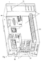
- Fig. 1 shows an exemplary embodiment of a central module 1 for a flexible expandable automation device for controlling and / or monitoring a technical process with a housing 2 on the housing lower part 3, the electronic assembly for the voltage supply of the central decoder assembly 1 is arranged and a housing front page. 4
- a serial interface 10 On the housing front side 4, a serial interface 10, an Ethernet interface 11, a, preferably coverable, device 40 as a slot for receiving retrofittable accessories and connecting elements 20 are arranged.
- the coverable device 40 with slots is provided for receiving replaceable circuit boards for further interface circuits, for example for an additional serial interface, as a socket for memory cards and / or for receiving a circuit board for a real-time clock.
- the front of the device 4 display means 13 for the display of the input and output modules which are designed as optical fibers.
- the light guides are intended to bundle the light at a fixed location and to transmit it contactlessly to the front side 4 of the central module 1. Due to the light bundled in the optical fibers used light is thus achieved in an advantageous manner that the light is emitted only at one point on the front side 4 of the central module 1.
- the central module 1 this is intended for wall mounting.
- the third printed circuit board and the lower housing part 3 are provided with at least one opening 66, which is provided for receiving fastening means, preferably screws, for wall mounting.
- Fig. 2 shows an exemplary embodiment of the circuit boards PCB1, PCB2, PCB3 of the central assembly 1 with thereon arranged electronic assemblies for a central unit, a power supply 60, an interface for the connection of external input and output modules and internal input and output modules.
- the three electronic modules of the central module 1 are each arranged on a separate circuit board PCB1, PCB2, PCB3.
- the third circuit board PCB3 with the power supply 60 of the central assembly 1, which faces the front panel 4 of the central assembly 1, is arranged according to the invention on the lower housing part 3 between the first circuit board PCB1 and the second circuit board PCB2.
- the printed circuit boards PCB1, PCB2, PCB3 are arranged substantially at right angles to one another, the third circuit board PCB3 accommodating the power supply 60 and further connection elements 20 for connecting the external input and output modules between the first, the central unit, the device for receiving of retrofittable accessories 40, connecting elements 20 and the Ethernet interface 11 receiving circuit board PCB1 and the second internal input and output modules receiving circuit board PCB2 is arranged.
- the first printed circuit board PCB1 has as complex constructed multi-layer printed circuit board preferably six layers, whereas the second, preferably four layers comprising PCB2 is cheaper to produce.
- the display means 13 are each formed from a first and a second light guide 51, 52.
- a detailed representation of the display means is exemplified in Fig. 5 shown.
- Fig. 3 shows the electrical and mechanical connection 30 of the right angle to each other PCBs PCB1, PCB2, PCB3 of the central assembly 1 with each other, the arrangement of the optical fibers 51, 52 on the first and second circuit board PCB1, PCB2 and a connector element 12 for a communication interface and a plug 5 for an input / output bus.
- the first and second printed circuit board PCB1, PCB2 in a preferred embodiment, a plurality of bent pins 31 which are guided through openings provided in the third PCB3 PCB and soldered, for example by means of a Wellenlötreaes ,
- the electrical connection between the printed circuit boards PCB1, PCB2, PCB3 is realized by the solder pins identified by the reference numeral 31.
- the opening 66 for receiving fastening means for wall mounting of the central assembly 1 is also shown by way of example.
- Fig. 4 shows an embodiment of the coverable device 40 located on the first circuit board PCB1 as a slot for receiving at least one retrofittable circuit board 44, wherein the circuit board 44 is provided for example for additional interfaces, memory cards and / or for receiving a real-time clock.
- the printed circuit board 44 to be retrofitted can be inserted, for example, into a socket which is formed from a U-shaped rail 45.
- the device 40 for receiving the circuit board 44 to be retrofitted is formed from two elongated rail-shaped elements 46, between which the printed circuit board 44 to be retrofitted is inserted.
- the elongated cuboidal elements 46 and the U-shaped rail 45 are bevelled or rounded at their inner ends of the printed circuit board 44 to be inserted, so as to facilitate the mounting of the printed circuit board 44.
- Fig. 5 shows an exemplary embodiment of a display means 13 of the central assembly 1, which is arranged on the second circuit board PCB2.
- the display means 13 is formed by the second light guide 52, which of the optical display elements 53, preferably light emitting diodes (see also Fig. 9 ) generates light and contactlessly transmits to the outlet openings 62.
- An aperture 64 holds the four identical parts 54 constructed second light guide 52 together and prevents crosstalk between the individual strands of the second light guide 52nd
- the second optical waveguide 52 may be constructed from a plurality of optical waveguide light parts 54 arranged one behind the other and configured such that simple and cost-effective injection molding tools can be used for its production.
- the structural design of the light guides 51, 52 is the Fig. 9 refer to.
- the arrangement of the identical parts 54 is achieved, for example, by stacking the identical parts 54 and a connection of the common parts, preferably via a pin-hole connection 55.
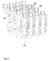
- An exemplary pin-hole connection 55 of stacked common parts 54 shows Fig. 6 ,
- the first light guide 51 disposed on the first printed circuit board PCB1 is also condensed by the first light guide 51 and the light bundled by the first light guide 51 is focused by the display elements 53 onto light exit surfaces 62 at a central location on the front 4 of the central module 1 is transmitted.
- the first light guide 51 is constructed in accordance with a preferred embodiment of a common part 54 and a carrier 56 receiving the identical part 54.
- the carrier 56 is intended to form together with the common part 54 a multiple light guide, which generates a plurality of light spots.
- the carrier 56 may also comprise connecting elements 57 for fastening the optical fiber 51 to the printed circuit board PCB1. The carrier 56 further prevents crosstalk between the individual strands of the light guide 54.
- Fig. 8 shows an exemplary embodiment of the receptacle 40 for the retrofittable accessories 40 of the central assembly 1 with the slots for receiving the same on the first and third circuit board PCB1, PCB3.
- the connector elements 58, 59 for connection of the retrofittable accessory 44, such as a communication interface or a real time clock on the first circuit board PCB1 and third circuit board PCB3 are denoted by reference numerals 58 and 59, respectively.
- Fig. 9 an exemplary sectional view of a common part 54 of the light guide is shown and illustrates the design of the common part 54 that is used as the first light guide 51.
- the identical part 54 consists of four individual light guide strands.
- the identical part is stiffened by webs 63.
- the light generated by the optical display elements 53 enters via entrance surfaces 65 of the identical part 54, is then reflected by total reflection at the surfaces 61 and exits at the outlet openings or in the surfaces 62.
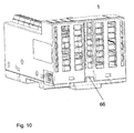
- Fig. 10 shows the central assembly 1 and the opening 66 for wall mounting of the assembly 1 by means of screws.
Landscapes
- Engineering & Computer Science (AREA)
- Microelectronics & Electronic Packaging (AREA)
- Automation & Control Theory (AREA)
- Computer Hardware Design (AREA)
- General Engineering & Computer Science (AREA)
- Human Computer Interaction (AREA)
- Combinations Of Printed Boards (AREA)
- Optical Couplings Of Light Guides (AREA)
- Mounting Of Printed Circuit Boards And The Like (AREA)
- Led Device Packages (AREA)
Abstract
Description
- Die Erfindung betrifft eine Zentralbaugruppe für ein flexibles erweiterbares Automatisierungsgerät gemäß dem Oberbegriff des Anspruches 1.
- Marktübliche oder in Patentdokumenten beschriebene erweiterbare Automatisierungsgeräte, auch als speicherprogrammierbare Steuerungen bekannt, sind an unterschiedlichste Automatisierungsaufgaben anpassbar und werden insbesondere im Bereich der industriellen Automatisierungstechnik und im Bereich der Schalt- und Steuerungstechnik eingesetzt.
- Diese Automatisierungssysteme sind üblicherweise modular aus einer Zentralbaugruppe, Kommunikationskopplern und Erweiterungsmodulen aufgebaut. Die Zentralbaugruppe gemäß dem bekannten Stand der Technik umfasst verschiedene Baugruppen, wie eine Zentraleinheit, auch als CPU bezeichnet, eine Spannungsversorgung, eine Schnittstelle für den Anschluss von externen Ein- und Ausgabemodulen und interne Ein- und Ausgabemodule.
- Bedingt durch die unterschiedlichen funktionellen und mechanischen Ausführungen der einzelnen Baugruppen der Zentralbaugruppe ist die Herstellung der Zentralbaugruppe, insbesondere bedingt durch mehrere aufeinander abzustimmende Lötprozesse zur Vermeidung der Zerstörung einzelner Bauelemente der Baugruppen, aufwendig und kostenintensiv.
- Der Erfindung liegt demgemäß die Aufgabe zugrunde, eine Zentralbaugruppe für ein flexibles erweiterbares Automatisierungsgerät, anzugeben, bei dem die vorgenannten Nachteile überwunden werden, und die Zentralbaugruppe, insbesondere in einfacher und kostengünstiger Weise, herstellbar ist.
- Diese Aufgabe wird erfindungsgemäß durch eine Zentralbaugruppe für ein flexibles erweiterbares Automatisierungsgerät mit den in Anspruch 1 angegebenen Merkmalen gelöst. Vorteilhafte Ausgestaltungen und Verbesserungen der erfindungsgemäßen Zentralbaugruppe sind in weiteren Ansprüchen und in der Beschreibung angegeben.
- Die erfindungsgemäße Zentralbaugruppe für ein flexibles erweiterbares Automatisierungsgerät umfasst ein Gehäuse, welches die verschiedenen Baugruppen, wie beispielsweise eine Zentraleinheit, eine Spannungsversorgung, eine Schnittstelle für den Anschluss von externen Ein- und Ausgabemodulen und interne Ein- und Ausgabemodule aufnimmt.
- Erfindungsgemäß ist die Zentralbaugruppe aus drei Elektronikbaugruppen aufgebaut, die jeweils auf einem separaten Träger, der als Leiterplatte oder Platine ausgeführt ist, angeordnet sind. Ein erster Träger ist für die Aufnahme der Elektronikbaugruppe der Zentraleinheit, ein zweite Träger zur Aufnahme der Elektronikbaugruppe der internen Ein- und Ausgabemodule sowie von Anzeigemitteln für die internen Ein- und Ausgabemodule und ein dritter Träger ist zur Aufnahme der Elektronikbaugruppe der Spannungsversorgung sowie der Schnittstelle für den Anschluss externer Module, wie beispielsweise externer Ein- und Ausgabemodule, vorgesehen. Der dritte Träger mit der Elektronikbaugruppe zur Spannungsversorgung der Zentralbaugruppe ist zwischen dem ersten und dem zweiten Träger angeordnet.
- Der erste und der zweite Träger der Zentralbaugruppe sind mit dem dritten Träger mechanisch und elektrisch verbunden. Vorzugsweise sind die Träger zur mechanischen und elektrischen Verbindung untereinander verlötet, beispielsweise wird die Verbindung der Träger mittels verlöteter Stifte realisiert. Dadurch entfällt die Steckverbindung zwischen den einzelnen Trägern und es wird eine bessere mechanische Stabilität erreicht.
- Die Träger sind in im wesentlichen rechtwinklig zueinander angeordnet, wobei der dritte die Spannungsversorgung der Zentralbaugruppe sowie die Schnittstelle für den Anschluss der externen Ein- und Ausgabemodule aufnehmende Träger zwischen dem zweiten die internen Ein- und Ausgabemodule aufnehmenden Träger und dem ersten die Zentraleinheit aufnehmenden Träger angeordnet ist.
- In einer bevorzugten Ausführungsform der Zentralbaugruppe weisen nur der zweite und der erste Träger Anschlusselemente, vorzugsweise steckbare oder verlötbare Klemmen, Steckerleisten oder Klemmenblöcke auf, beispielsweise zum Anschluss externer Signale weiterer externer Erweiterungsmodule, die beispielsweise als Ein- und Ausgabemodule ausgeführt sind. Somit wird eine Reduktion der Steckverbindungen zwischen den drei Elektronikbaugruppen bzw. Trägern erreicht, da die Träger miteinander verlötet sind und die elektrische Verbindung zwischen den Trägern ohne zusätzliche Steckverbindungen gewährleistet ist.
- Erfindungsgemäß ist der erste Träger, bedingt durch die darauf befindlichen Bauelemente der Zentraleinheit, gegenüber dem zweiten und dritten Träger als komplexe mehrlagige Leiterplatte ausgeführt und die Anzahl der Lagen des ersten Trägers ist gegenüber der Anzahl der Lagen des zweiten und dritten Trägers erhöht.
- In einer bevorzugten Ausführungsform der Zentralbaugruppe sind auf dem ersten Träger auch die Ethernet-Schnittstelle und/oder eine, vorzugsweise abdeckbare, Vorrichtung als Steckplatz für die Aufnahme von nachrüstbarem Zubehör vorgesehen. Das nachrüstbare Zubehör können austauschbare Leiterplatten für weitere Interfaceschaltungen, Speicherkarten oder zur Aufnahme einer Echtzeituhr sein.
- Die auf dem ersten und zweiten Träger befindlichen Anzeigemittel für die Anzeige der Ein- und Ausgabemodule sind als Lichtleiter ausgeführt und dafür vorgesehen, das Licht zu bündeln und kontaktlos auf die Frontseite der Zentralbaugruppe zu übertragen.
- Durch den vereinfachten mechanischen Aufbau der Zentralbaugruppe bezüglich der Integration der funktional unterschiedlichen Baugruppen entsprechend ihren Funktionen auf drei Trägern gestaltet sich die Herstellung der Zentralbaugruppe kostengünstig, da die auf den verschiedenen Trägern angeordneten Elektronikbaugruppen mit dem jeweils optimal geeigneten Lötprozess gefertigt werden können.
- Die mehrlagige Leiterplatte (erster Träger), welche mit den Bauteilen für die Zentraleinheit, wie beispielsweise Mikrocontroller, Speicher und Logikbausteinen, bestückt ist, wird vorzugsweise beidseitig im SMD Prozess bestückt und gelötet, oder in Kombination mit einem zusätzlichen selektiven Lötprozess für die Verbindungsstifte zur mechanischen und elektrischen Verbindung der Leiterplatten untereinander.
- Die Leiterplatte, welche die Elektronikbaugruppe der internen Ein- und Ausgabemodule aufnimmt (zweiter Träger), kann in Abhängigkeit von den verwendeten Bauteilen beidseitig im SMD Prozess, oder einseitig im SMD Prozess und auf der anderen Seite im Wellenlötprozess oder zweiseitig im SMD Prozess mit zusätzlichem selektiven Löten der bedrahteten Bauteile bestückt und gelötet werden.
- Die Leiterplatte für die Spannungsversorgung und die Schnittstelle für den Anschluss externer Module (dritter Träger) kann je nach verwendeten Bauteilen ein- oder zweiseitig im SMD Prozess bestückt und gelötet werden. Bedrahtete Bauteile sowie die Verbindungen zwischen alle drei LP können dagegen mittels eines Wellenlötprozesses verarbeitet werden.
- Anhand der in den folgenden Figuren dargestellten Ausführungsformen sollen die Erfindung sowie vorteilhafte Ausgestaltungen, Verbesserungen und weitere Vorteile der Erfindung näher erläutert und beschrieben werden.
- Es zeigen:
- Fig. 1
- eine beispielhafte Ausführung einer Zentralbaugruppe für ein flexibles er- weiterbares Automatisierungsgerät,
- Fig. 2
- eine beispielhafte Ausführung der Leiterplatten der Zentralbaugruppe mit den darauf angeordneten Elektronikbaugruppen,
- Fig. 3
- eine beispielhafte Verbindungslösung der Leiterplatten untereinander,
- Fig. 4
- eine Ausführungsform der auf der ersten Leiterplatte befindlichen Vorricht- und als Steckplatz für die Aufnahme von nachrüstbarem Zubehör,
- Fig. 5
- eine beispielhafte Ausführung eines Anzeigemittels der Zentralbaugruppe, welches auf der zweiten Leiterplatte angeordnet ist,
- Fig. 6
- eine beispielhafte Zapfen-Loch-Verbindung von aufeinandergestapelten Gleichteilen,
- Fig. 7
- eine beispielhafte Ausführung eines Anzeigemittels, welches auf der ers- ten Leiterplatte angeordnet ist,
- Fig. 8
- eine beispielhafte Ausführung der Aufnahme des nachrüstbaren Zubehörs und der Steckplätze zur Aufnahme desselben,
- Fig. 9
- eine beispielhafte Ausgestaltung eines Gleichteiles des Lichtleiters, und
- Fig. 10
- die Zentralbaugruppe mit einem beispielhaften Durchbruch zur Wandbe- festigung mittels Schrauben.
-
Fig. 1 zeigt eine beispielhafte Ausführung einer Zentralbaugruppe 1 für ein flexibles erweiterbares Automatisierungsgerät zur Steuerung und/oder Überwachung eines technischen Prozesses mit einem Gehäuse 2 auf dessen Gehäuseunterteil 3 die Elektronikbaugruppe für die Spannungs-Versorgung der Zentralabbaugruppe 1 angeordnet ist sowie einer Gehäusefrontseite 4. - An der Gehäusefrontseite 4 sind eine serielle Schnittstelle 10, eine Ethernet-Schnittstelle 11, eine, vorzugsweise abdeckbare, Vorrichtung 40 als Steckplatz für die Aufnahme von nachrüstbarem Zubehör sowie Anschlusselemente 20 angeordnet.
- Die abdeckbare Vorrichtung 40 mit Steckplätzen ist für die Aufnahme von austauschbaren Leiterplatten für weitere Interfaceschaltungen, beispielsweise für eine zusätzliche serielle Schnittstelle, als Sockel für Speicherkarten und/oder zur Aufnahme einer Leiterplatte für eine Echtzeituhr vorgesehen.
- Weiterhin weist die Gerätefrontseite 4 Anzeigemittel 13 für die Anzeige der Ein- und Ausgabemodule auf, die als Lichtleiter ausgeführt sind. Die Lichtleiter sind dafür vorgesehen, das Licht an einer festgelegten Stelle zu bündeln und kontaktlos auf die Frontseite 4 der Zentralbaugruppe 1 zu übertragen. Durch das in den verwendeten Lichtleitern gebündelte Licht wird somit in vorteilhafter Weise erreicht, dass das Licht nur an einer Stelle auf der Frontseite 4 der Zentralbaugruppe 1 ausgegeben wird.
- In einer besonderen Ausführungsform der Zentralbaugruppe 1 ist diese für eine Wandmontage vorgesehen. Dazu sind die dritte Leiterplatte und das Gehäuseunterteil 3 mit wenigstens einem Durchbruch 66 versehen, der zur Aufnahme von Befestigungsmitteln, vorzugsweise Schrauben, für die Wandmontage vorgesehen ist.
-
Fig. 2 zeigt eine beispielhafte Ausführung der Leiterplatten PCB1, PCB2, PCB3 der Zentralbaugruppe 1 mit darauf angeordneten Elektronikbaugruppen für eine Zentraleinheit, eine Spannungsversorgung 60, eine Schnittstelle für den Anschluss von externen Ein- und Ausgabemodulen und interne Ein- und Ausgabemodule. - Die drei Elektronikbaugruppen der Zentralbaugruppe 1 sind jeweils auf einer separaten Leiterplatte PCB1, PCB2, PCB3 angeordnet. Die dritte Leiterplatte PCB3 mit der Spannungsversorgung 60 der Zentralabbaugruppe 1, die der Gerätefrontseite 4 der Zentralbaugruppe 1 gegenüberliegt, ist erfindungsgemäß auf dem Gehäuseunterteil 3 zwischen der ersten Leiterplatte PCB1 und der zweiten Leiterplatte PCB2 angeordnet.
- Die Leiterplatten PCB1, PCB2, PCB3 sind im wesentlichen in einem rechten Winkel zueinander angeordnet, wobei die dritte die Spannungsversorgung 60 sowie weitere Anschlusselemente 20 für den Anschluss der externen Ein- und Ausgabemodule aufnehmende Leiterplatte PCB3 zwischen der ersten die Zentraleinheit, die Vorrichtung für die Aufnahme von nachrüstbarem Zubehör 40, Anschlusselemente 20 und die Ethernet-Schnittstelle 11 aufnehmende Leiterplatte PCB1 und der zweiten die internen Ein- und Ausgabemodule aufnehmenden Leiterplatte PCB2 angeordnet ist.
- Die erste Leiterplatte PCB1 weist als komplex aufgebaute mehrlagige Leiterplatte vorzugsweise sechs Lagen auf, wohingegen die zweite, vorzugsweise vier Lagen umfassenden, Leiterplatte PCB2 kostengünstiger herstellbar ist.
- Auf der ersten und zweiten Leiterplatte PCB1, PCB2 der Zentralbaugruppe 1 sind jeweils die Anzeigemittel 13 aus einem ersten und einem zweiten Lichtleiter 51, 52 gebildet. Eine detaillierte Darstellung der Anzeigemittel ist beispielhaft in
Fig. 5 gezeigt. -
Fig. 3 zeigt die elektrische und mechanische Verbindung 30 der im rechten Winkel aufeinander stehenden Leiterplatten PCB1, PCB2, PCB3 der Zentralbaugruppe 1 miteinander, die Anordnung der Lichtleiter 51, 52 auf der ersten und zweiten Leiterplatte PCB1, PCB2 sowie ein Steckerelement 12 für eine Kommunikationsschnittstelle und einen Stecker 5 für einen Ein-/Ausgabebus. - Zur Verbindung der Leiterplatten PCB1, PCB2, PCB3 untereinander weisen die erste und zweite Leiterplatte PCB1, PCB2 in einer bevorzugten Ausführungsform eine Vielzahl von gebogenen Stiften 31 auf, die durch in der dritten Leiterplatte PCB3 vorgesehene Öffnungen geführt und, beispielsweise mittels eines Wellenlötprozesses, verlötet sind.
- Die elektrische Verbindung zwischen den Leiterplatten PCB1, PCB2, PCB3 wird durch die mit dem Bezugszeichen 31 gekennzeichneten Lötstifte realisiert.
- Durch die vorab beschriebene elektrische und mechanische Verbindung 30, 31 der in der Zentralbaugruppe 1 angeordneten Leiterplatten PCB1, PCB2, PCB3 entfallen teuere Steckverbindungen und es wird eine bessere mechanische Stabilität erreicht.
- Auf der dritten Leiterplatte PCB3 ist weiterhin beispielhaft der Durchbruch 66 zur Aufnahme von Befestigungsmitteln für eine Wandmontage der Zentralbaugruppe 1 gezeigt.
-
Fig. 4 zeigt eine Ausführungsform der auf der ersten Leiterplatte PCB1 befindlichen abdeckbaren Vorrichtung 40 als Steckplatz für die Aufnahme von wenigstens einer nachrüstbaren Leiterplatte 44, wobei die Leiterplatte 44 beispielsweise für zusätzliche Schnittstellen, Speicherkarten und/oder zur Aufnahme einer Echtzeituhr vorgesehen ist. - In einer ersten Ausführungsform 42 der Vorrichtung 40 kann die nachzurüstende Leiterplatte 44, beispielsweise in einen Sockel, der aus einer U-förmig ausgebildeten Schiene 45 gebildet wird, eingeschoben werden.
- In einer weiteren Ausführungsform 43 wird die Vorrichtung 40 zur Aufnahme der nachzurüstenden Leiterplatte 44 aus zwei langgestreckten schienenförmigen Elementen 46 gebildet, zwischen die die nachzurüstende Leiterplatte 44 eingeschoben wird.
- Zur Aufnahme der Leiterplatte 44 sind die langgestreckten quaderförmigen Elemente 46 bzw. die U-förmig ausgebildete Schiene 45 an ihren innenliegenden der einzuschiebenden Leiterplatte 44 zugeneigten Enden abgeschrägt oder abgerundet, um so die Aufnahme der Leiterplatte 44 zu erleichtern.
-
Fig. 5 zeigt eine beispielhafte Ausführung eines Anzeigemittels 13 der Zentralbaugruppe 1, welches auf der zweiten Leiterplatte PCB2 angeordnet ist. Das Anzeigemittel 13 wird durch den zweiten Lichtleiter 52 gebildet, der das von optischen Anzeigeelementen 53, vorzugsweise Leuchtdioden(siehe auchFig. 9 ) erzeugte Licht bündelt und kontaktlos an die Austrittsöffnungen 62 überträgt. Eine Blende 64 hält den aus vier Gleichteilen 54 aufgebauten zweiten Lichtleiter 52 zusammen und verhindert ein Übersprechen zwischen den einzelnen Strängen des zweiten Lichtleiters 52. - Der zweite Lichtleiter 52 kann aus mehreren hintereinander angeordneten Lichtleitergleichteilen 54 aufgebaut und so ausgestaltet sein, dass zu seiner Herstellung einfache und kostengünstige Spritzgusswerkzeuge verwendbar sind. Die konstruktive Ausgestaltung der Lichtleiter 51, 52 ist der
Fig. 9 zu entnehmen. - Die Anordnung der Gleichteile 54 wird, beispielsweise durch Aufeinanderstapeln der Gleichteile 54 und eine Verbindung der Gleichteile, vorzugsweise über eine Zapfen-Loch-Verbindung 55, erreicht. Eine beispielhafte Zapfen-Loch-Verbindung 55 von aufeinandergestapelten Gleichteilen 54 zeigt
Fig. 6 . - In
Fig. 7 ist der erste Lichtleiter 51 gezeigt, der auf der ersten Leiterplatte PCB1 angeordnet ist, wobei auch das von optischen Anzeigeelementen 53 erzeugte Licht vom ersten Lichtleiter 51 gebündelt wird und das vom ersten Lichtleiter 51 gebündelte Licht von den Anzeigeelementen 53 auf Lichtaustrittsflächen 62 an einer zentralen Stelle auf der Frontseite 4 der Zentralbaugruppe 1 übertragen wird. - Der erste Lichtleiter 51 ist gemäß einer bevorzugten Ausführungsform aus einem Gleichteil 54 und einem das Gleichteil 54 aufnehmenden Träger 56 aufgebaut. Der Träger 56 ist dafür vorgesehen gemeinsam mit dem Gleichteil 54 einen Mehrfachlichtleiter zu bilden, der mehrere Lichtpunkte erzeugt. Weiterhin kann der Träger 56 auch Verbindungselemente 57 zur Befestigung des Lichtleiters 51 an der Leiterplatte PCB1 aufweisen. Der Träger 56 verhindert ferner ein Übersprechen zwischen den einzelnen Strängen des Lichtleiters 54.
-
Fig. 8 zeigt eine beispielhafte Ausführung der Aufnahme 40 für das nachrüstbare Zubehör 40 der Zentralbaugruppe 1 mit den Steckplätzen zur Aufnahme desselben auf der ersten bzw. dritten Leiterplatte PCB1, PCB3. Die Steckerelemente 58, 59 zum Anschluss des nachrüstbaren Zubehörs 44, wie beispielsweise einer Kommunikationsschnittstelle oder einer Echtzeituhr auf der ersten Leiterplatte PCB1 bzw. dritten Leiterplatte PCB3 sind mit den Bezugszeichen 58 bzw. 59 gekennzeichnet. - In
Fig. 9 ist eine beispielhafte Schnittdarstellung eines Gleichteiles 54 des Lichtleiters dargestellt und verdeutlicht die Ausgestaltung des Gleichteiles 54, dass als erster Lichtleiter 51 verwendet wird. Das Gleichteil 54 besteht aus vier einzelnen Lichtleitersträngen. Das Gleichteil ist durch Stege 63 ausgesteift. - Das das von den optischen Anzeigeelementen 53 erzeugte Licht tritt über Eintrittsflächen 65 des Gleichteils 54 ein, wird dann über Totalreflexion an den Flächen 61 reflektiert und tritt an den Austrittsöffnungen bzw. in den Flächen 62 aus.
-
Fig. 10 zeigt die Zentralbaugruppe 1 und den Durchbruch 66 zur Wandbefestigung der Baugruppe 1 mittels Schrauben. -
- 1
- Zentralbaugruppe
- 2
- Gehäuse
- 3
- Gehäuseunterteil
- 4
- Gehäusefrontseite
- 5
- Stecker für Ein-/Ausgabebus
- 10
- serielle Schnittstelle
- 11
- Ethernet-Schnittstelle
- 12, 58, 59
- Steckerelement zum Anschluss von nachrüstbarem Zubehör
- 13
- Anzeigemittel
- 20
- Anschlusselemente
- 30
- Verbindung der Träger untereinander
- 31
- Stifte
- 40
- Vorrichtung als Steckplatz für die Aufnahme von nachrüstbarem Zubehör
- 41
- Öffnung zur Aufnahme zusätzlicher Leiterplatten
- 42
- erste Ausführungsform zur Aufnahme einer zusätzlichen Leiterplatte
- 43
- zweite Ausführungsform zur Aufnahme einer zusätzlichen Leiterplatte
- 44
- zusätzliche Leiterplatte
- 45
- Sockel, U-förmige Schiene
- 46
- langgestrecktes quaderförmiges Element
- 51
- erster Lichtleiter
- 52
- zweiter Lichtleiter
- 53
- Anzeigeelement
- 54
- Gleichteil des Lichtleiters
- 55
- Zapfen-Loch-Verbindung
- 56
- Träger
- 57
- Verbindungselement
- 60
- Spannungsversorgung
- 61
- Reflexionsfläche
- 62
- Austrittsöffnung, Austrittsfläche
- 63
- Steg
- 64
- Blende
- 65
- Eintrittsöffnung
- 66
- Durchbruch
- PCB1
- erster Träger zur Aufnahme der Elektronikbaugruppe Zentraleinheit
- PCB2
- zweiter Träger zur Aufnahme Elektronikbaugruppe der internen Ein- und Ausgabemodule
- PCB3
- dritter Träger zur Aufnahme der Elektronikbaugruppe der Spannungsver- sorgung sowie der Schnittstelle für den Anschluss von externen Ein- und Ausgabemodulen
Claims (10)
- Zentralbaugruppe für ein flexibles erweiterbares Automatisierungsgerät umfassend ein Gehäuse (2), welches eine Zentraleinheit, eine Spannungsversorgung (60), eine Schnittstelle für den Anschluss von externen Ein- und Ausgabemodulen und interne Ein- und Ausgabemodule aufnimmt, dadurch gekennzeichnet, dass die Zentralbaugruppe drei Elektronikbaugruppen umfasst, die jeweils auf einem separaten Träger (PCB1), (PCB2), (PCB3) angeordnet sind, wobei ein dritter Träger (PCB3) zwischen einem ersten und einem zweiten Träger (PCB1), (PCB2) angeordnet ist, der erste Träger (PCB1) für die Aufnahme der Elektronikbaugruppe der Zentraleinheit vorgesehen ist, der zweite Träger (PCB2) zur Aufnahme Elektronikbaugruppe der internen Ein- und Ausgabemodule vorgesehen ist und der dritte Träger (PCB3) zur Aufnahme der Elektronikbaugruppe der Spannungsversorgung (60) sowie der Schnittstelle für den Anschluss von externen Ein- und Ausgabemodulen vorgesehen ist.
- Zentralbaugruppe nach Anspruch 1, dadurch gekennzeichnet, dass der erste und zweite Träger (PCB1), (PCB2) mit dem dritten Träger (PCB3) mechanisch und elektrisch verbunden sind.
- Zentralbaugruppe nach einen der vorherigen Ansprüche, dadurch gekennzeichnet, dass die Träger (PCB1), (PCB2), (PCB3) zur elektrischen und mechanische Verbindung (30) untereinander verlötet sind.
- Zentralbaugruppe nach einen der vorherigen Ansprüche, dadurch gekennzeichnet, dass die Träger (PCB1), (PCB2), (PCB3) im wesentlichen rechtwinklig zueinander angeordnet sind, wobei der dritte die Spannungsversorgung sowie die Schnittstelle für den Anschluss der externen Ein- und Ausgabemodule aufnehmenden Träger (PCB3) zwischen dem ersten die Zentraleinheit aufnehmenden Träger (PCB1) und dem zweiten die internen Ein- und Ausgabemodule aufnehmenden Träger (PCB2) angeordnet ist.
- Zentralbaugruppe nach einen der vorherigen Ansprüche, dadurch gekennzeichnet, dass der erste und der zweite Träger (PCB1), (PCB2) steckbare oder verlötbare Klemmen zum Anschluss externer Signale aufweisen.
- Zentralbaugruppe nach einen der vorherigen Ansprüche, dadurch gekennzeichnet, dass der erste Träger (PCB1) gegenüber den zweiten und dritten Träger (PCB2), (PCB3) als komplexe mehrlagige Leiterplatte ausgeführt und die Anzahl der Lagen des ersten Trägers (PCB1) gegenüber der Anzahl der Lagen des zweiten und dritten Trägers (PCB2), (PCB3) erhöht ist.
- Zentralbaugruppe nach einen der vorherigen Ansprüche, dadurch gekennzeichnet, dass der erste Träger (PCB1) eine Ethernet-Schnittstelle (11) aufweist.
- Zentralbaugruppe nach einen der vorherigen Ansprüche, dadurch gekennzeichnet, dass der erste Träger (PCB1) eine serielle Schnittstelle (10) aufweist.
- Zentralbaugruppe nach einem der vorherigen Ansprüche, dadurch gekennzeichnet, dass der erste Träger (PCB1) eine Vorrichtung (40) als Steckplatz für die Aufnahme von nachrüstbarem Zubehör aufweist.
- Zentralbaugruppe nach einem der vorherigen Ansprüche, dadurch gekennzeichnet, dass auf dem ersten und zweiten Träger (PCB1), (PCB2) als Lichtleiter (51), (52) ausgeführte Anzeigemittel (13) vorgesehen sind, die das von optischen Anzeigeelementen 53 erzeugte Licht bündeln und kontaktlos auf die Frontseite der Zentralbaugruppe übertragen.
Applications Claiming Priority (1)
| Application Number | Priority Date | Filing Date | Title |
|---|---|---|---|
| DE102008058060A DE102008058060A1 (de) | 2008-11-18 | 2008-11-18 | Zentralbaugruppe für ein flexibles erweiterbares Automatisierungsgerät |
Publications (2)
| Publication Number | Publication Date |
|---|---|
| EP2187716A1 true EP2187716A1 (de) | 2010-05-19 |
| EP2187716B1 EP2187716B1 (de) | 2011-12-21 |
Family
ID=41500953
Family Applications (1)
| Application Number | Title | Priority Date | Filing Date |
|---|---|---|---|
| EP09012894A Active EP2187716B1 (de) | 2008-11-18 | 2009-10-13 | Zentralbaugruppe für ein flexibles erweiterbares Automatisierungsgerät |
Country Status (5)
| Country | Link |
|---|---|
| US (1) | US8472172B2 (de) |
| EP (1) | EP2187716B1 (de) |
| CN (2) | CN201374871Y (de) |
| AT (1) | ATE538628T1 (de) |
| DE (1) | DE102008058060A1 (de) |
Cited By (2)
| Publication number | Priority date | Publication date | Assignee | Title |
|---|---|---|---|---|
| EP2736312A1 (de) * | 2012-11-27 | 2014-05-28 | Siemens Aktiengesellschaft | Automatisierungsgerät mit Kühlkörper |
| EP4633299A1 (de) * | 2024-04-12 | 2025-10-15 | Theben AG | Reiheneinbaugerät und verfahren zur herstellung eines reiheneinbaugeräts |
Families Citing this family (6)
| Publication number | Priority date | Publication date | Assignee | Title |
|---|---|---|---|---|
| US9055687B2 (en) * | 2010-08-20 | 2015-06-09 | Rockwell Automation Technologies, Inc. | Input/output circuits and devices having physically corresponding status indicators |
| US9538687B2 (en) * | 2013-06-12 | 2017-01-03 | Menara Network, Inc. | High-density rack unit systems and methods |
| DE102013111578B4 (de) * | 2013-10-21 | 2019-04-18 | Wago Verwaltungsgesellschaft Mbh | Elektronikmodul |
| DE102014108527A1 (de) * | 2014-06-17 | 2015-12-17 | Endress+Hauser Flowtec Ag | Nachrüstbare Echtzeituhr für ein Feldgerät |
| EP3521954B1 (de) * | 2018-02-05 | 2025-05-21 | ABB Schweiz AG | Flexible erweiterbare automatisierungsvorrichtung mit hot-swap-fähigen e/a-einheiten |
| DE102023127910A1 (de) * | 2023-10-12 | 2025-04-17 | Dspace Gmbh | Modul eingerichtet zum Einschieben in einen Baugruppenträger |
Citations (4)
| Publication number | Priority date | Publication date | Assignee | Title |
|---|---|---|---|---|
| DE3838353A1 (de) | 1988-11-11 | 1990-05-17 | Rexroth Mannesmann Gmbh | Elektrischer verstaerker zum ansteuern von ventilen |
| US5519573A (en) * | 1994-12-27 | 1996-05-21 | Intel Corporation | I/O riser card for motherboard in a personal computer/server |
| US5552965A (en) | 1993-04-02 | 1996-09-03 | Saia Ag | Control apparatus having a compact and accessible arrangement of printed circuit boards |
| US20070293954A1 (en) | 2006-01-23 | 2007-12-20 | Watlow Electric Manufacturing Company | Compact modular card system and communications protocols for a power controller |
Family Cites Families (7)
| Publication number | Priority date | Publication date | Assignee | Title |
|---|---|---|---|---|
| US5172311A (en) * | 1988-11-11 | 1992-12-15 | Mannesmann Rexroth Gmbh | Electrical amplifier for controlling valves |
| US6530790B1 (en) * | 1998-11-24 | 2003-03-11 | Teradyne, Inc. | Electrical connector |
| US6608564B2 (en) * | 2000-01-25 | 2003-08-19 | Hewlett-Packard Development Company, L.P. | Removable memory cartridge system for use with a server or other processor-based device |
| EP1557075A4 (de) * | 2002-10-22 | 2010-01-13 | Sullivan Jason | Nicht-peripheres verarbeitungssteuermodul mit verbesserten wärmeableiteigenschaften |
| DE10256648A1 (de) * | 2002-12-03 | 2004-06-17 | Endress + Hauser Wetzer Gmbh + Co Kg | Signalverarbeitungseinheit für die Prozessautomatisierungstechnik zur Montage an einer Hutschiene |
| DE102004056363B4 (de) * | 2004-11-22 | 2018-10-04 | Abb Ag | Flexibles erweiterbares Automatisierungsgerät |
| DE202006006615U1 (de) * | 2006-04-22 | 2006-09-07 | Phoenix Contact Gmbh & Co. Kg | Elektronikgehäuse |
-
2008
- 2008-11-18 DE DE102008058060A patent/DE102008058060A1/de not_active Withdrawn
-
2009
- 2009-01-21 CN CN200920001721U patent/CN201374871Y/zh not_active Expired - Fee Related
- 2009-10-13 EP EP09012894A patent/EP2187716B1/de active Active
- 2009-10-13 AT AT09012894T patent/ATE538628T1/de active
- 2009-11-17 US US12/619,885 patent/US8472172B2/en active Active
- 2009-11-18 CN CN200910223082.5A patent/CN101738943B/zh active Active
Patent Citations (4)
| Publication number | Priority date | Publication date | Assignee | Title |
|---|---|---|---|---|
| DE3838353A1 (de) | 1988-11-11 | 1990-05-17 | Rexroth Mannesmann Gmbh | Elektrischer verstaerker zum ansteuern von ventilen |
| US5552965A (en) | 1993-04-02 | 1996-09-03 | Saia Ag | Control apparatus having a compact and accessible arrangement of printed circuit boards |
| US5519573A (en) * | 1994-12-27 | 1996-05-21 | Intel Corporation | I/O riser card for motherboard in a personal computer/server |
| US20070293954A1 (en) | 2006-01-23 | 2007-12-20 | Watlow Electric Manufacturing Company | Compact modular card system and communications protocols for a power controller |
Cited By (3)
| Publication number | Priority date | Publication date | Assignee | Title |
|---|---|---|---|---|
| EP2736312A1 (de) * | 2012-11-27 | 2014-05-28 | Siemens Aktiengesellschaft | Automatisierungsgerät mit Kühlkörper |
| US9338876B2 (en) | 2012-11-27 | 2016-05-10 | Siemens Aktiengesellschaft | Automation device having a heatsink |
| EP4633299A1 (de) * | 2024-04-12 | 2025-10-15 | Theben AG | Reiheneinbaugerät und verfahren zur herstellung eines reiheneinbaugeräts |
Also Published As
| Publication number | Publication date |
|---|---|
| EP2187716B1 (de) | 2011-12-21 |
| CN101738943A (zh) | 2010-06-16 |
| CN201374871Y (zh) | 2009-12-30 |
| CN101738943B (zh) | 2014-10-29 |
| DE102008058060A1 (de) | 2010-05-20 |
| ATE538628T1 (de) | 2012-01-15 |
| US20100134967A1 (en) | 2010-06-03 |
| US8472172B2 (en) | 2013-06-25 |
Similar Documents
| Publication | Publication Date | Title |
|---|---|---|
| EP2187716B1 (de) | Zentralbaugruppe für ein flexibles erweiterbares Automatisierungsgerät | |
| DE102008058090B4 (de) | Ein-/Ausgabemodul für ein Automatisierungsgerät | |
| DE102008064674B4 (de) | Zentralbaugruppe für ein flexibles erweiterbares Automatisierungsgerät | |
| DE102013111578B4 (de) | Elektronikmodul | |
| EP2277242B1 (de) | Messerleisten-kontaktierung über zwischenleiterplatten | |
| DE102007019805A1 (de) | Kabelkasten | |
| EP1930992A2 (de) | Blockiervorrichtung gegen Fehlsteckungen bei Leiterplattensteckverbindern | |
| EP0909121B1 (de) | Elektronisches Ein-/Ausgabemodul | |
| DE102016000762A1 (de) | Elektrogerät | |
| DE202018105037U1 (de) | Filterverbinder | |
| DE2722736C2 (de) | Mehrpolige Anschlußleiste | |
| DE102011076377A1 (de) | Elektrische Reihenklemmenanordnung | |
| EP2614691A1 (de) | Leiterplatte zum bestücken mit leuchtkörpern | |
| DE102011105712B4 (de) | Ankopplungseinrichtung für Kommunikationsgeräte | |
| WO2006067028A2 (de) | Leiterplatte mit wenigstens eine metallisierte seitliche öffnung in der stirnseite und anordnung mindestens zwei solcher leiterplatten | |
| DE202007005562U1 (de) | Elektrische Anschlussvorrichtung | |
| DE102005032730B4 (de) | Anordnung mit einem Träger zur Aufnahme und Halterung einer Baugruppe eines Automatisierungsgerätes | |
| DE202018106823U1 (de) | Busfähiges aneinanderreihbares Funktionsmodul | |
| EP0304902B1 (de) | Anordnung zum Ändern und/oder Reparieren von Flachbaugruppen bei Bestückung mit SMD-Bausteinen | |
| DE102011118360A1 (de) | Vorrichtung zur Steuerung einer Mehrzahl von Antriebseinheiten und gesteuertes Antriebssystem für eine automatisierte Anlage | |
| DE102014102976A1 (de) | Leiterplatte und Anordnung zum elektrischen Verbinden einer Betriebselektronik | |
| DE2304456A1 (de) | Einschubsystem fuer elektronikbaugruppen | |
| DE112016004062B4 (de) | Verfahren zur Herstellung einer elektrooptischen Schnittstelle, elektrooptische Schnittstelle und Steuergerät | |
| EP0664582A1 (de) | Anschlussmodul | |
| DE10204549A1 (de) | Adapter zur elektrischen/elektronischen Kopplung eines Motorprüfstandes mit einem an einen Kraftfahrzeugmotor angeschlossenen Motorsteuergerät |
Legal Events
| Date | Code | Title | Description |
|---|---|---|---|
| PUAI | Public reference made under article 153(3) epc to a published international application that has entered the european phase |
Free format text: ORIGINAL CODE: 0009012 |
|
| AK | Designated contracting states |
Kind code of ref document: A1 Designated state(s): AT BE BG CH CY CZ DE DK EE ES FI FR GB GR HR HU IE IS IT LI LT LU LV MC MK MT NL NO PL PT RO SE SI SK SM TR |
|
| AX | Request for extension of the european patent |
Extension state: AL BA RS |
|
| 17P | Request for examination filed |
Effective date: 20100701 |
|
| 17Q | First examination report despatched |
Effective date: 20100803 |
|
| GRAP | Despatch of communication of intention to grant a patent |
Free format text: ORIGINAL CODE: EPIDOSNIGR1 |
|
| GRAS | Grant fee paid |
Free format text: ORIGINAL CODE: EPIDOSNIGR3 |
|
| GRAA | (expected) grant |
Free format text: ORIGINAL CODE: 0009210 |
|
| AK | Designated contracting states |
Kind code of ref document: B1 Designated state(s): AT BE BG CH CY CZ DE DK EE ES FI FR GB GR HR HU IE IS IT LI LT LU LV MC MK MT NL NO PL PT RO SE SI SK SM TR |
|
| REG | Reference to a national code |
Ref country code: GB Ref legal event code: FG4D Free format text: NOT ENGLISH |
|
| REG | Reference to a national code |
Ref country code: CH Ref legal event code: EP |
|
| REG | Reference to a national code |
Ref country code: AT Ref legal event code: REF Ref document number: 538628 Country of ref document: AT Kind code of ref document: T Effective date: 20120115 |
|
| REG | Reference to a national code |
Ref country code: IE Ref legal event code: FG4D |
|
| REG | Reference to a national code |
Ref country code: DE Ref legal event code: R096 Ref document number: 502009002236 Country of ref document: DE Effective date: 20120216 |
|
| REG | Reference to a national code |
Ref country code: NL Ref legal event code: VDEP Effective date: 20111221 |
|
| PG25 | Lapsed in a contracting state [announced via postgrant information from national office to epo] |
Ref country code: LT Free format text: LAPSE BECAUSE OF FAILURE TO SUBMIT A TRANSLATION OF THE DESCRIPTION OR TO PAY THE FEE WITHIN THE PRESCRIBED TIME-LIMIT Effective date: 20111221 Ref country code: NO Free format text: LAPSE BECAUSE OF FAILURE TO SUBMIT A TRANSLATION OF THE DESCRIPTION OR TO PAY THE FEE WITHIN THE PRESCRIBED TIME-LIMIT Effective date: 20120321 |
|
| LTIE | Lt: invalidation of european patent or patent extension |
Effective date: 20111221 |
|
| PG25 | Lapsed in a contracting state [announced via postgrant information from national office to epo] |
Ref country code: LV Free format text: LAPSE BECAUSE OF FAILURE TO SUBMIT A TRANSLATION OF THE DESCRIPTION OR TO PAY THE FEE WITHIN THE PRESCRIBED TIME-LIMIT Effective date: 20111221 Ref country code: GR Free format text: LAPSE BECAUSE OF FAILURE TO SUBMIT A TRANSLATION OF THE DESCRIPTION OR TO PAY THE FEE WITHIN THE PRESCRIBED TIME-LIMIT Effective date: 20120322 Ref country code: SE Free format text: LAPSE BECAUSE OF FAILURE TO SUBMIT A TRANSLATION OF THE DESCRIPTION OR TO PAY THE FEE WITHIN THE PRESCRIBED TIME-LIMIT Effective date: 20111221 Ref country code: HR Free format text: LAPSE BECAUSE OF FAILURE TO SUBMIT A TRANSLATION OF THE DESCRIPTION OR TO PAY THE FEE WITHIN THE PRESCRIBED TIME-LIMIT Effective date: 20111221 Ref country code: NL Free format text: LAPSE BECAUSE OF FAILURE TO SUBMIT A TRANSLATION OF THE DESCRIPTION OR TO PAY THE FEE WITHIN THE PRESCRIBED TIME-LIMIT Effective date: 20111221 Ref country code: SI Free format text: LAPSE BECAUSE OF FAILURE TO SUBMIT A TRANSLATION OF THE DESCRIPTION OR TO PAY THE FEE WITHIN THE PRESCRIBED TIME-LIMIT Effective date: 20111221 |
|
| PG25 | Lapsed in a contracting state [announced via postgrant information from national office to epo] |
Ref country code: CY Free format text: LAPSE BECAUSE OF FAILURE TO SUBMIT A TRANSLATION OF THE DESCRIPTION OR TO PAY THE FEE WITHIN THE PRESCRIBED TIME-LIMIT Effective date: 20111221 |
|
| REG | Reference to a national code |
Ref country code: IE Ref legal event code: FD4D |
|
| PG25 | Lapsed in a contracting state [announced via postgrant information from national office to epo] |
Ref country code: IE Free format text: LAPSE BECAUSE OF FAILURE TO SUBMIT A TRANSLATION OF THE DESCRIPTION OR TO PAY THE FEE WITHIN THE PRESCRIBED TIME-LIMIT Effective date: 20111221 Ref country code: EE Free format text: LAPSE BECAUSE OF FAILURE TO SUBMIT A TRANSLATION OF THE DESCRIPTION OR TO PAY THE FEE WITHIN THE PRESCRIBED TIME-LIMIT Effective date: 20111221 Ref country code: CZ Free format text: LAPSE BECAUSE OF FAILURE TO SUBMIT A TRANSLATION OF THE DESCRIPTION OR TO PAY THE FEE WITHIN THE PRESCRIBED TIME-LIMIT Effective date: 20111221 Ref country code: BG Free format text: LAPSE BECAUSE OF FAILURE TO SUBMIT A TRANSLATION OF THE DESCRIPTION OR TO PAY THE FEE WITHIN THE PRESCRIBED TIME-LIMIT Effective date: 20120321 Ref country code: SK Free format text: LAPSE BECAUSE OF FAILURE TO SUBMIT A TRANSLATION OF THE DESCRIPTION OR TO PAY THE FEE WITHIN THE PRESCRIBED TIME-LIMIT Effective date: 20111221 Ref country code: IS Free format text: LAPSE BECAUSE OF FAILURE TO SUBMIT A TRANSLATION OF THE DESCRIPTION OR TO PAY THE FEE WITHIN THE PRESCRIBED TIME-LIMIT Effective date: 20120421 |
|
| PG25 | Lapsed in a contracting state [announced via postgrant information from national office to epo] |
Ref country code: RO Free format text: LAPSE BECAUSE OF FAILURE TO SUBMIT A TRANSLATION OF THE DESCRIPTION OR TO PAY THE FEE WITHIN THE PRESCRIBED TIME-LIMIT Effective date: 20111221 Ref country code: PT Free format text: LAPSE BECAUSE OF FAILURE TO SUBMIT A TRANSLATION OF THE DESCRIPTION OR TO PAY THE FEE WITHIN THE PRESCRIBED TIME-LIMIT Effective date: 20120423 Ref country code: PL Free format text: LAPSE BECAUSE OF FAILURE TO SUBMIT A TRANSLATION OF THE DESCRIPTION OR TO PAY THE FEE WITHIN THE PRESCRIBED TIME-LIMIT Effective date: 20111221 |
|
| PLBE | No opposition filed within time limit |
Free format text: ORIGINAL CODE: 0009261 |
|
| STAA | Information on the status of an ep patent application or granted ep patent |
Free format text: STATUS: NO OPPOSITION FILED WITHIN TIME LIMIT |
|
| PG25 | Lapsed in a contracting state [announced via postgrant information from national office to epo] |
Ref country code: DK Free format text: LAPSE BECAUSE OF FAILURE TO SUBMIT A TRANSLATION OF THE DESCRIPTION OR TO PAY THE FEE WITHIN THE PRESCRIBED TIME-LIMIT Effective date: 20111221 |
|
| 26N | No opposition filed |
Effective date: 20120924 |
|
| REG | Reference to a national code |
Ref country code: DE Ref legal event code: R097 Ref document number: 502009002236 Country of ref document: DE Effective date: 20120924 |
|
| BERE | Be: lapsed |
Owner name: ABB A.G. Effective date: 20121031 |
|
| PG25 | Lapsed in a contracting state [announced via postgrant information from national office to epo] |
Ref country code: ES Free format text: LAPSE BECAUSE OF FAILURE TO SUBMIT A TRANSLATION OF THE DESCRIPTION OR TO PAY THE FEE WITHIN THE PRESCRIBED TIME-LIMIT Effective date: 20120401 |
|
| PG25 | Lapsed in a contracting state [announced via postgrant information from national office to epo] |
Ref country code: MC Free format text: LAPSE BECAUSE OF NON-PAYMENT OF DUE FEES Effective date: 20121031 |
|
| PG25 | Lapsed in a contracting state [announced via postgrant information from national office to epo] |
Ref country code: FI Free format text: LAPSE BECAUSE OF FAILURE TO SUBMIT A TRANSLATION OF THE DESCRIPTION OR TO PAY THE FEE WITHIN THE PRESCRIBED TIME-LIMIT Effective date: 20111221 |
|
| PG25 | Lapsed in a contracting state [announced via postgrant information from national office to epo] |
Ref country code: BE Free format text: LAPSE BECAUSE OF NON-PAYMENT OF DUE FEES Effective date: 20121031 |
|
| PG25 | Lapsed in a contracting state [announced via postgrant information from national office to epo] |
Ref country code: MT Free format text: LAPSE BECAUSE OF FAILURE TO SUBMIT A TRANSLATION OF THE DESCRIPTION OR TO PAY THE FEE WITHIN THE PRESCRIBED TIME-LIMIT Effective date: 20111221 |
|
| PG25 | Lapsed in a contracting state [announced via postgrant information from national office to epo] |
Ref country code: TR Free format text: LAPSE BECAUSE OF FAILURE TO SUBMIT A TRANSLATION OF THE DESCRIPTION OR TO PAY THE FEE WITHIN THE PRESCRIBED TIME-LIMIT Effective date: 20111221 |
|
| PG25 | Lapsed in a contracting state [announced via postgrant information from national office to epo] |
Ref country code: SM Free format text: LAPSE BECAUSE OF FAILURE TO SUBMIT A TRANSLATION OF THE DESCRIPTION OR TO PAY THE FEE WITHIN THE PRESCRIBED TIME-LIMIT Effective date: 20111221 Ref country code: LU Free format text: LAPSE BECAUSE OF NON-PAYMENT OF DUE FEES Effective date: 20121013 |
|
| REG | Reference to a national code |
Ref country code: CH Ref legal event code: PL |
|
| GBPC | Gb: european patent ceased through non-payment of renewal fee |
Effective date: 20131013 |
|
| PG25 | Lapsed in a contracting state [announced via postgrant information from national office to epo] |
Ref country code: GB Free format text: LAPSE BECAUSE OF NON-PAYMENT OF DUE FEES Effective date: 20131013 Ref country code: CH Free format text: LAPSE BECAUSE OF NON-PAYMENT OF DUE FEES Effective date: 20131031 Ref country code: LI Free format text: LAPSE BECAUSE OF NON-PAYMENT OF DUE FEES Effective date: 20131031 Ref country code: HU Free format text: LAPSE BECAUSE OF FAILURE TO SUBMIT A TRANSLATION OF THE DESCRIPTION OR TO PAY THE FEE WITHIN THE PRESCRIBED TIME-LIMIT Effective date: 20091013 |
|
| PG25 | Lapsed in a contracting state [announced via postgrant information from national office to epo] |
Ref country code: MK Free format text: LAPSE BECAUSE OF FAILURE TO SUBMIT A TRANSLATION OF THE DESCRIPTION OR TO PAY THE FEE WITHIN THE PRESCRIBED TIME-LIMIT Effective date: 20111221 |
|
| REG | Reference to a national code |
Ref country code: FR Ref legal event code: PLFP Year of fee payment: 7 |
|
| REG | Reference to a national code |
Ref country code: AT Ref legal event code: MM01 Ref document number: 538628 Country of ref document: AT Kind code of ref document: T Effective date: 20141013 |
|
| PG25 | Lapsed in a contracting state [announced via postgrant information from national office to epo] |
Ref country code: AT Free format text: LAPSE BECAUSE OF NON-PAYMENT OF DUE FEES Effective date: 20141013 |
|
| REG | Reference to a national code |
Ref country code: FR Ref legal event code: PLFP Year of fee payment: 8 |
|
| PGFP | Annual fee paid to national office [announced via postgrant information from national office to epo] |
Ref country code: FR Payment date: 20161020 Year of fee payment: 8 |
|
| PGFP | Annual fee paid to national office [announced via postgrant information from national office to epo] |
Ref country code: IT Payment date: 20161024 Year of fee payment: 8 |
|
| REG | Reference to a national code |
Ref country code: FR Ref legal event code: ST Effective date: 20180629 |
|
| PG25 | Lapsed in a contracting state [announced via postgrant information from national office to epo] |
Ref country code: FR Free format text: LAPSE BECAUSE OF NON-PAYMENT OF DUE FEES Effective date: 20171031 |
|
| PG25 | Lapsed in a contracting state [announced via postgrant information from national office to epo] |
Ref country code: IT Free format text: LAPSE BECAUSE OF NON-PAYMENT OF DUE FEES Effective date: 20171013 |
|
| PGFP | Annual fee paid to national office [announced via postgrant information from national office to epo] |
Ref country code: DE Payment date: 20251021 Year of fee payment: 17 |