EP2187513B1 - Electronic circuit arranged to control voltage applied to a load - Google Patents
Electronic circuit arranged to control voltage applied to a load Download PDFInfo
- Publication number
- EP2187513B1 EP2187513B1 EP20080019880 EP08019880A EP2187513B1 EP 2187513 B1 EP2187513 B1 EP 2187513B1 EP 20080019880 EP20080019880 EP 20080019880 EP 08019880 A EP08019880 A EP 08019880A EP 2187513 B1 EP2187513 B1 EP 2187513B1
- Authority
- EP
- European Patent Office
- Prior art keywords
- voltage
- load
- switch
- switch element
- electronic circuit
- Prior art date
- Legal status (The legal status is an assumption and is not a legal conclusion. Google has not performed a legal analysis and makes no representation as to the accuracy of the status listed.)
- Active
Links
- 239000003990 capacitor Substances 0.000 claims description 29
- 238000001514 detection method Methods 0.000 claims description 27
- 238000000034 method Methods 0.000 claims description 5
- 238000012935 Averaging Methods 0.000 claims 2
- 230000000977 initiatory effect Effects 0.000 claims 1
- 238000005259 measurement Methods 0.000 description 6
- 230000001681 protective effect Effects 0.000 description 6
- 101100189862 Saccharomyces cerevisiae (strain ATCC 204508 / S288c) PEP8 gene Proteins 0.000 description 4
- 238000010586 diagram Methods 0.000 description 4
- 101100049526 Saccharomyces cerevisiae (strain ATCC 204508 / S288c) VPS13 gene Proteins 0.000 description 3
- 230000001419 dependent effect Effects 0.000 description 3
- 238000010792 warming Methods 0.000 description 2
- 230000001680 brushing effect Effects 0.000 description 1
- 230000015556 catabolic process Effects 0.000 description 1
- 230000003247 decreasing effect Effects 0.000 description 1
- 238000007599 discharging Methods 0.000 description 1
- 230000000694 effects Effects 0.000 description 1
- 230000001939 inductive effect Effects 0.000 description 1
- 238000012986 modification Methods 0.000 description 1
- 230000004048 modification Effects 0.000 description 1
- 230000002035 prolonged effect Effects 0.000 description 1
- 230000002123 temporal effect Effects 0.000 description 1
- XLYOFNOQVPJJNP-UHFFFAOYSA-N water Substances O XLYOFNOQVPJJNP-UHFFFAOYSA-N 0.000 description 1
Images


Classifications
-
- H—ELECTRICITY
- H02—GENERATION; CONVERSION OR DISTRIBUTION OF ELECTRIC POWER
- H02P—CONTROL OR REGULATION OF ELECTRIC MOTORS, ELECTRIC GENERATORS OR DYNAMO-ELECTRIC CONVERTERS; CONTROLLING TRANSFORMERS, REACTORS OR CHOKE COILS
- H02P7/00—Arrangements for regulating or controlling the speed or torque of electric DC motors
- H02P7/06—Arrangements for regulating or controlling the speed or torque of electric DC motors for regulating or controlling an individual dc dynamo-electric motor by varying field or armature current
- H02P7/18—Arrangements for regulating or controlling the speed or torque of electric DC motors for regulating or controlling an individual dc dynamo-electric motor by varying field or armature current by master control with auxiliary power
- H02P7/24—Arrangements for regulating or controlling the speed or torque of electric DC motors for regulating or controlling an individual dc dynamo-electric motor by varying field or armature current by master control with auxiliary power using discharge tubes or semiconductor devices
- H02P7/28—Arrangements for regulating or controlling the speed or torque of electric DC motors for regulating or controlling an individual dc dynamo-electric motor by varying field or armature current by master control with auxiliary power using discharge tubes or semiconductor devices using semiconductor devices
- H02P7/285—Arrangements for regulating or controlling the speed or torque of electric DC motors for regulating or controlling an individual dc dynamo-electric motor by varying field or armature current by master control with auxiliary power using discharge tubes or semiconductor devices using semiconductor devices controlling armature supply only
- H02P7/29—Arrangements for regulating or controlling the speed or torque of electric DC motors for regulating or controlling an individual dc dynamo-electric motor by varying field or armature current by master control with auxiliary power using discharge tubes or semiconductor devices using semiconductor devices controlling armature supply only using pulse modulation
-
- G—PHYSICS
- G05—CONTROLLING; REGULATING
- G05F—SYSTEMS FOR REGULATING ELECTRIC OR MAGNETIC VARIABLES
- G05F1/00—Automatic systems in which deviations of an electric quantity from one or more predetermined values are detected at the output of the system and fed back to a device within the system to restore the detected quantity to its predetermined value or values, i.e. retroactive systems
- G05F1/10—Regulating voltage or current
-
- H—ELECTRICITY
- H02—GENERATION; CONVERSION OR DISTRIBUTION OF ELECTRIC POWER
- H02M—APPARATUS FOR CONVERSION BETWEEN AC AND AC, BETWEEN AC AND DC, OR BETWEEN DC AND DC, AND FOR USE WITH MAINS OR SIMILAR POWER SUPPLY SYSTEMS; CONVERSION OF DC OR AC INPUT POWER INTO SURGE OUTPUT POWER; CONTROL OR REGULATION THEREOF
- H02M3/00—Conversion of dc power input into dc power output
- H02M3/02—Conversion of dc power input into dc power output without intermediate conversion into ac
- H02M3/04—Conversion of dc power input into dc power output without intermediate conversion into ac by static converters
- H02M3/10—Conversion of dc power input into dc power output without intermediate conversion into ac by static converters using discharge tubes with control electrode or semiconductor devices with control electrode
- H02M3/145—Conversion of dc power input into dc power output without intermediate conversion into ac by static converters using discharge tubes with control electrode or semiconductor devices with control electrode using devices of a triode or transistor type requiring continuous application of a control signal
- H02M3/155—Conversion of dc power input into dc power output without intermediate conversion into ac by static converters using discharge tubes with control electrode or semiconductor devices with control electrode using devices of a triode or transistor type requiring continuous application of a control signal using semiconductor devices only
- H02M3/156—Conversion of dc power input into dc power output without intermediate conversion into ac by static converters using discharge tubes with control electrode or semiconductor devices with control electrode using devices of a triode or transistor type requiring continuous application of a control signal using semiconductor devices only with automatic control of output voltage or current, e.g. switching regulators
- H02M3/158—Conversion of dc power input into dc power output without intermediate conversion into ac by static converters using discharge tubes with control electrode or semiconductor devices with control electrode using devices of a triode or transistor type requiring continuous application of a control signal using semiconductor devices only with automatic control of output voltage or current, e.g. switching regulators including plural semiconductor devices as final control devices for a single load
- H02M3/1588—Conversion of dc power input into dc power output without intermediate conversion into ac by static converters using discharge tubes with control electrode or semiconductor devices with control electrode using devices of a triode or transistor type requiring continuous application of a control signal using semiconductor devices only with automatic control of output voltage or current, e.g. switching regulators including plural semiconductor devices as final control devices for a single load comprising at least one synchronous rectifier element
-
- Y—GENERAL TAGGING OF NEW TECHNOLOGICAL DEVELOPMENTS; GENERAL TAGGING OF CROSS-SECTIONAL TECHNOLOGIES SPANNING OVER SEVERAL SECTIONS OF THE IPC; TECHNICAL SUBJECTS COVERED BY FORMER USPC CROSS-REFERENCE ART COLLECTIONS [XRACs] AND DIGESTS
- Y02—TECHNOLOGIES OR APPLICATIONS FOR MITIGATION OR ADAPTATION AGAINST CLIMATE CHANGE
- Y02E—REDUCTION OF GREENHOUSE GAS [GHG] EMISSIONS, RELATED TO ENERGY GENERATION, TRANSMISSION OR DISTRIBUTION
- Y02E10/00—Energy generation through renewable energy sources
- Y02E10/50—Photovoltaic [PV] energy
- Y02E10/56—Power conversion systems, e.g. maximum power point trackers
Definitions
- the present invention is concerned with electronic circuits that are arranged to control a voltage applied to a load and it specifically is concerned with such electronic circuits in which a supply voltage to be applied to the load is repeatedly switched-on and switched-off in a controlled manner.
- Such a circuit is e.g. used to control the voltage applied to a motor as load by varying the on and off periods (i.e. the duty cycle) of a pulse-width modulation (PWM) of the voltage supply according to a control signal.
- PWM pulse-width modulation
- a motor control circuit is disclosed that is used to control the speed of a left and a right motor of a small vehicle, the left and the right motor driving the left and the right wheel of the small vehicle, respectively.
- Document US 4,914,376 discloses an actuation device for a small electric appliance having a circuit arrangement having a closed-loop control function.
- a threshold function of the circuit arrangement provides a pulsed voltage at a load by switching on and off a transistor.
- the closed-loop control function may comprise an RC element providing an integral action on the voltage supplied at the load.
- the integrated signal is provided at a threshold function for switching the transistor in dependence on a reference signal.
- An electronic circuit as proposed is connectable to a load and a voltage source.
- a connected state is hence the state in which the electronic circuit is connected to the load and the voltage source.
- the electronic circuit has an off state and an active state.
- the active state comprises a switch-on phase and a control phase.
- the electronic circuit comprises a controllable load switch element, a voltage detection circuitry, and a switch-on circuitry.
- the load switch element is in the connected state arranged between the voltage source and the load. When the load switch element is switched on, a supply voltage provided by the voltage supply is provided at the load and when the load switch element is switched off no voltage is provided at the load.
- the switch-on circuitry is coupled to the load switch element and is arranged to switch on the load switch element during a determined period of time after initialization of the switch-on phase, which initialization happens by closing a switch. For this period of time, the switch-on circuitry forces the load switch element to stay switched on.
- the voltage detection circuitry takes over the control of the load switch element and repeatedly switches on and off the load switch element in dependence on the average voltage provided at the load.
- the proposed circuit switches on and off the load switch element as long as the supply voltage provided by the voltage supply is higher than the average voltage to be provided at the load.
- variations in the supply voltage can be absorbed and any respective variations in the load state of the load are avoided.
- an average voltage can be applied to a load so that over time the voltage provided at the load and hence the load state stays essentially constant and does not follow the usual voltage breakdown known from discharging batteries or accumulators. This leads also to the effect that the energy provided at the load is controlled to stay at a constant level, so that a prolonged battery (accumulator) lifetime results.
- the electronic circuit may further comprise a switch-off circuitry that is coupled to the load switch element.
- the switch-off circuitry forces the load switch element to be switched-off after initialization of a switch-off phase, which initialization may happen by opening the same switch again that was closed to initialize the switch-on phase.
- the closed-loop control that is performed by the voltage detection circuitry in the control phase is energized by the voltage applied to the load, just opening the switch will not stop the closed-loop control.
- the switch-off phase is to be initialized by the same switch that is used to initialize the switch-on phase, the switch-off circuitry allows this by forcing the load switch element to stay switched off.
- the voltage supply of the voltage detection circuit will stop for a period long enough so that the voltage detection circuit de-energizes and the closed-loop control stops. This allows for using a single switch that needs to be operated by a user of an appliance in which the electronic circuit is used, which renders the electronic circuit and hence the appliance as simple and easy to operate.
- the switch-on circuitry comprises a series arrangement of a first capacitor and a third resistor and further a first switch element that has a control side that is coupled in between the first capacitor and the third resistor.
- the first capacitor is coupled to the switch and hence starts to charge when the switch-on phase is initialized. A current is then flowing through the capacitor and into the control side of the first switch element, which first switch element becomes switched on.
- the first switch element is arranged between ground potential and a control side of the load switch element. While the first switch element is switched on, essentially ground potential is provided at the control side of the load switch element, which forces the load switch element to stay switched on.
- the current flow through the first capacitor is determined by the time constant of the series arrangement of first capacitor and third resistor. A period of time during which the load switch element is forced to be switched on by the switch-on circuitry can thus be determined.
- the period of time is chosen such that the load is not boosting up to a load state beyond a targeted load state, which could happen as the full supply voltage provided by the voltage supply is larger than the average voltage to be applied to the load.
- the switch-off circuitry comprises a second switch element that has a control side that is coupled to the switch and that is arranged between the voltage source and the control side of the load switch element.
- the second switch element becomes switched on and hence forces the load switch element to stay switched off.
- the voltage detection circuit is arranged to measure the voltage provided at the load and to control the load switch element in such a way so that the average voltage provided at the load stays essentially at a predetermined level (the target voltage) during the control phase. Constancy of the average voltage may depend on a hysteresis and the accuracy of the voltage detection circuit.
- the voltage detection circuit comprises a voltage comparator element that has a voltage input at which the average voltage provided at the load is provided. The voltage comparator element compares the voltage at the voltage input with a reference voltage and provides a voltage at the voltage output in dependence on the comparison result. The voltage output is coupled to the control side of the load switch element.
- the voltage detection circuit comprises a low pass filter that is arranged to average the pulsed voltage provided at the load and to provide the averaged voltage at the voltage input of the voltage comparator element.
- the invention is also concerned with an electric appliance in which a circuit as proposed is utilized.
- an electric appliance can be, e.g., an electric toothbrush, an oral irrigator, a pocket lamp or flashlight, an electronic tool such as a powered (cordless) screwdriver, a (cordless) handblender, a powered safety razor, or an electric dry shaver.
- a load e.g., a DC motor or a lamp can be employed. In such an electric device, the load state of the load is kept constant and the energy of a battery or an accumulator is efficiently used.
- Fig. 1 is a circuitry diagram of an exemplary embodiment of an electronic circuit C as proposed.
- the circuit C is connectable to a load M such as a motor and a voltage source B such as a battery or an accumulator (secondary battery) or a battery and/or accumulator pack.
- the voltage source B may alternatively also be an AC/DC converter that is connected to mains voltage.
- a single battery is shown as voltage source B, but instead of a single battery, a series arrangement of batteries can be used (further batteries are indicated by a dotted battery symbol).
- the circuit C is shown in the connected state in which the circuit C is connected to the load M and the voltage source B.
- the circuit C comprises a switch S1, a voltage detection circuitry VD, a switch-on circuitry Son, a switch-off circuitry Soff, a filter circuitry F, and a load switch element TL with a respective protective circuit D.
- the load switch element TL is controlled in such a way that it becomes repeatedly conductive and non-conductive so that a supply voltage V S that is larger than the voltage to be applied to the load M is applied as a pulsed voltage pV S to the load M.
- the protective circuit D comprises a series arrangement of a first resistor R1 and a second resistor R2.
- the switch-on circuitry Son further comprises an eighth resistor R8 as input resistance for the control side of the first switch element.
- the switch-off circuitry Soff comprises a second switch element T2, a fifth resistor R5 and a fourth resistor R4.
- the filter circuitry F comprises a parallel arrangement of an overvoltage protection diode D1 and a second capacitor C2.
- the voltage detection circuitry VD comprises a voltage comparator element VR1 that is energized by the voltage to be measured and further a low pass filter comprising a sixth resistor R6, a seventh resistor R7, a third capacitor C3, and a fourth capacitor C4.
- the sixth resistor R6, the seventh resistor R7 and the third and fourth capacitors C3 and C4 are used to smooth (or average) the pulsed voltage pV S so that an averaged voltage V A is applied to a voltage input VI of the voltage comparator element VR1.
- the voltage comparator element VR1 further has a voltage output VO and a ground connection VGND. Measurement points TP1, TP2, TP3, TP4, and TP5 are also indicated in Fig. 1 .
- a series arrangement of the load switch element TL in the shown embodiment, the load switch element TL is realized as a MOSFET) and the load M is arranged in parallel to the voltage source B such that the plus pole of the voltage source B is connected to a first side (source electrode) of the load switch element TL and the minus pole (ground potential) of the voltage source B is connected to a first side of the load M.
- a second side (drain electrode) of the load switch element TL is connected with a second side of the load M.
- the filter circuitry F is connected to the load M in the usual way so that the cathode of the overvoltage protection diode D1 is connected to the second side of the load M and the anode of the overvoltage protection diode D1 is connected to the first side of the load M.
- a first side of the second capacitor C2 is connected to the first side of the load M and the second side of the second capacitor C2 is connected to the second side of the load M.
- the filter circuit F is a standard filter circuit to protect a load against voltage peaks.
- a first side of the first resistor R1 of the protective circuit D is connected to the plus pole of the voltage source B and the second side of the first resistor R1 is connected to the control side (gate electrode) of the load switch element TL and to the first side of the second resistor R2 of the protective circuit D.
- a first side (emitter) of the second switch element T2 (in the shown embodiment realized as a pnp transistor) is coupled to the plus pole of the voltage source B and a second side (collector) of the second switch element T2 is connected with the first side of the second resistor R2.
- the first side of the switch S1 (in the shown embodiment realized as a manual on/off switch) is coupled to the plus pole of the voltage source B and a second side of the switch S1 is coupled to the first side of the fifth resistor R5.
- the second side of the fifth resistor R5 is connected to a control side (basis) of the second switch element T2 (the fifth resistor R5 is, as is known in the art, used as basis resistor for the second switch element).
- the second side of the switch S1 is coupled to ground potential via the fourth resistor R4 and is further coupled to the first side of the first capacitor C1.
- the second side of the first capacitor C1 is coupled via the third resistor R3 to ground potential and also via the eight resistor R8 to the control side (basis) of the first switch element T1 (which is in the shown embodiment realized as a npn transistor).
- the eighth resistor R8 (again, used as basis resistor for the first switch element) and the first switch element T1 may be realized by a single electronic component such as a digital transistor as is e.g. provided by Rohm Co., Ltd., Kyoto, Japan.
- the fifth resistor R5 and the second switch element T2 could also be realized by a digital transistor.
- a first side (collector) of the first switch element T1 is connected to the second side of the second resistor R2 and a second side (emitter) of the first switch element T1 is connected to ground potential.
- the second side of the load M is coupled to a low pass filter that comprises the sixth resistor R6, the seventh resistor R7, and the third and fourth capacitors C3 and C4.
- the second side of the load M is coupled to the first side of the seventh resistor R7.
- the second side of the seventh resistor R7 is coupled to ground potential via the fourth capacitor C4 and to the first side of the sixth resistor R6.
- the second side of the sixth resistor R6 is coupled to ground potential via the third capacitor C3 and to the voltage input VI of the voltage comparator element VR1.
- the ground connector VGND of the voltage comparator element VR1 is coupled to ground potential and the voltage output VO of the voltage comparator element VR1 is coupled to the first side (collector) of the first switch element T1 and to the second side of the second resistor R2.
- the voltage comparator element VR1 is a low-voltage detection IC from the BU48XXG Series provided by Rohm Co., Ltd., Kyoto, Japan. This reset IC has no external voltage supply, compares the input voltage with an internal reference voltage, has a high accuracy of 1%, a preset hysteresis, and is very cost efficient.
- this reset IC can also be implemented by a discrete realization of the underlying circuit arrangement of this reset IC or by any other reset IC, specifically a more complex reset IC (or discrete realization of such), e.g. a reset IC that allows to choose between various hysteresis values and/or a reset IC that allows comparison with various voltages.
- the shown circuit C is used to enable a closed loop control of the average voltage V A applied to the load M such that the average voltage is V A constant (due to a hysteresis of the voltage comparator element VR1, the constancy of the average voltage V A means a constancy within the limits given by the hysteresis value) even if the voltage V S provided by the voltage source B varies over time.
- the voltage V S provided by the voltage source B is applied to the load M in an intermittent or PWM way.
- the load switch element TL is controlled to switch off the voltage applied to the load M for a controlled period during a repeating cycle such that the average voltage V A stays constant.
- the voltage source B is chosen such that it provides a voltage V S that is higher than the average voltage V A required by the load M.
- the voltage source B provides full voltage, the off-periods are relatively long (this can be seen from Fig. 2A , which is discussed further below), while the off-periods become shorter when the voltage provided by the voltage source B drops (which can be seen from Fig. 2B ).
- the voltage may drop in case the voltage source B is realized as a battery or an accumulator that is considerably discharged. As an example, the voltage source B may deliver 3 Volt as full voltage.
- the motor will rotate at a frequency proportional to the supply voltage.
- a control method as such is known, e.g. by using a microcontroller that is externally powered.
- the purpose of the proposed circuit C is to allow for using a voltage detection circuitry VD (and specifically a voltage comparator element VR1) that is energized by the measured (averaged) voltage while only a single switch S1 is needed to start the closed loop control and to stop the closed loop control. Further, the purpose of the circuit C is to use a very simple and cost-efficient electronic structure, e.g. to use a simple reset IC as discussed above, as voltage comparator element VR1.
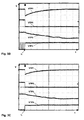
- Figs. 2A, 2B , and 2C voltages measured at the measurement points TP1, TP2, TP3, TP4, and TP5 indicated in Fig. 1 of an exemplary circuit realization (see Example 1 below) are shown, where voltage V is depicted against time t. Voltage curves are depicted for the switch-on (or start-up) phase ( Figs. 2A, 2B , and 2C ) and for the switch-off phase ( Figs.
- FIGS. 2A and 3A show the voltage curves for a full voltage provided by the voltage source
- Figs. 2B and 3B show the voltage curves for a somewhat reduces mid voltage value that is still above the average voltage required by the load M
- Figs. 2C and 3C show the voltage curves for a low voltage lying below the internal reference voltage of the voltage comparator element VR1.
- the circuit C In an off-state of the circuit C, the circuit C is connected to the voltage source B and the load M, while the load M is not energized (no current is flowing through the load M), and the switch S1 is open.
- the voltage detection circuitry VD As the voltage detection circuitry VD is energized by the measured (averaged) voltage V A applied to the load M, it would be impossible to start the closed loop control as the voltage to be measured is not present and hence the voltage detection circuitry VD is not energized.
- the proposed circuit C comprises the switch-on circuitry Son as described above. When the switch S1 is closed (at time instant to indicated in Figs.
- the period of time T is chosen such that any boosting up of the load M beyond a targeted load state (given by the average voltage V A to be applied to the load M) is essentially avoided.
- the protective circuit D comprising the first resistor R1 and the second resistor R2, is arranged such that in this situation also the load switch element TL becomes conductive while the first switch element T1 is conductive independent on any voltage output (whether present or not present) of the voltage comparator element VR1.
- the motor is energized and the full battery voltage is provided at the motor.
- the averaged voltage V A (voltage curve VTP3 in Figs. 2A-2C ) is provided through the low pass filter R6, R7, C3, C4 at the voltage input VI of the voltage comparator element VR1 so that the voltage comparator element VR1 is energized.
- the voltage curve for the temporal behavior of VTP3 during the switch-on phase is shown in Figs.
- the first switch element T1 is conductive and hence while the load switch element TL is conductive, the voltage provided by the voltage source B is provided at the load M and the load M is energized.
- the load M is a motor
- the motor warms up (i.e. starts to move).
- the time constant ⁇ is chosen such that a secure warming up of the load M is guaranteed.
- the time constant ⁇ is chosen such that the full battery voltage is applied to the motor only for a limited period of time T (e.g.
- the switch-on circuitry Son is relevant for the switch-on phase of the circuit C to enable the energizing of the voltage comparator element VR1 and the warming up of the load M.
- the first resistor R1 of the protective circuit D functions as a failsafe protection element (pull-up functionality) and the second resistor R2 functions as a current delimiter element.
- the voltage comparator element VR1 receives at its voltage input VI the voltage provided at the load M after it is averaged by the low pass filter R6, R7, C3, C4.
- the hysteresis of the voltage comparator element VR1 can be seen from the voltage curve VPT3 in Figs. 2A and 2B .
- the voltage comparator element VR1 compares the voltage provided at its voltage input VI with a reference voltage (e.g. 2 Volts) and either provides ground potential at its voltage output VO in case the voltage provided at the voltage input VI is below the reference voltage or provides the received voltage at its voltage output if the received voltage is above the reference voltage.
- a reference voltage e.g. 2 Volts
- the voltage comparator element VR1 has a certain hysteresis, as said before.
- a thereof dependent voltage shown in voltage curve VPT4 in Figs. 2A-2C
- the control side (gate) of the load switch element TL which - in case the supply voltage V S is above the average voltage that should be applied to the motor, as is shown in Figs. 2A and 2B - is hence periodically switched on and off to keep the average voltage V A provided at the load M constant even in case the voltage provided by the voltage source B varies.
- the first switch element T1 and the second switch element T2 are non-conductive.
- the switch-off circuitry Soff is provided.
- the switch S1 is opened (the voltage curve VTP5 shown in Figs. 3A , 3B, and 3C indicates this switching at time instant t 1 ).
- the second switch element T2 becomes conductive, which in turn forces the load switch element TL to become non-conductive independent on the output of the voltage comparator element VR1 (without the switch-off circuitry Soff, the closed loop control would simply continue if the switch S1 is opened).
- the load M remains without voltage supply. In case the load M is a motor, the motor slows down and finally stops.
- Voltage curve VPT3 shown in Figs. 3A , 3B, and 3C shows the averaged voltage that is generated by the motor of Example 1 during it slows down.
- the fully charged first capacitor C1 discharges over the fourth resistor R4 of the switch-off circuitry Soff, as can be seen from the respective voltage curves VTP1 shown in Figs. 3A , 3B, and 3C .
- the voltage supply of the voltage comparator element VR1 stops when neither a voltage is applied at the load M nor a voltage is generated by the load M (e.g.
- Voltage curves VTP4 in Figs. 3A , 3B, and 3C show that the voltage comparator element VR1 stops switching the output voltage as the voltage provided at its voltage input VI (shown in voltage curves VPT3) drops below the reference voltage.
- the voltage shown by voltage curve VPT4 is measured at measurement point TP4 and is hence put on high voltage when the second switch element T2 becomes conductive. Hence, after a short period of time T, the switch-off phase is completed and no voltage is present at the load M or applied to the voltage comparator element VR1. The circuit C is then again in the off-state.
- the circuit can be switched-on as was described above.
- the voltage comparator element VR1 comprises a selector with which a reference voltage of the voltage comparator element VR1 can be selected, so that it is enabled to use the proposed circuit also to provide one of several constant voltages to a load.
- a selector with which a reference voltage of the voltage comparator element VR1 can be selected, so that it is enabled to use the proposed circuit also to provide one of several constant voltages to a load.
- different light intensities can then be selected.
- different motor speeds can be selected.
- the circuit is e.g. utilized in an oral irrigator, different water pressures can then be selected.
- different brushing speeds can be selected.
- the circuit C is electronically dimensioned to operate with a typical DC motor as is used for electric toothbrushes as load M.
- the average voltage V A that should be applied to this motor is 2 Volt.
- voltage source B a series arrangement of two standard AA batteries (or accumulators), each providing 1.5 Volt, is used, so that a full voltage provided by this series arrangement is 3 Volt.
- voltage comparator element VR1 a low voltage detector IC BU4820G from the BU48XXG Series as provided by Rohm Co., Ltd., Kyoto, Japan, was utilized. This low voltage detector IC compares input voltages with an internal reference voltage of 2 Volt and has an accuracy of ⁇ 1%.
- switch load element TL a MOSFET IRLML6401 as provided by International Rectifier, EI Segundo, CA, USA, was used.
- first and second switching elements T1 and T2 universal pnp and npn transistors such as BC848B and BC858C, respectively, can be used.
- the first and the third resistors R1 and R3 had a resistance of 100 kilo-Ohm
- the second and fourth resistors R2 and R4 had a resistance of 1 kilo-Ohm
- the resistances of the fifth, sixth, seventh and eighth resistor R5, R6, R7, and R8 were 200 kilo-Ohm, 511 Ohm, 221 Ohm and 10 kilo-Ohm, respectively.
- first diode D1 a LL4148 diode was used as first diode D1.
- the first capacitor C1 had a capacitance of 0.47 micro-Farad
- the second capacitor C2 had a capacitance of 0.15 micro-Farad
- the third and fourth capacitors C3 and C4 had each a capacitance of 4.7 micro-Farad.
- the voltage curves as shown in Figs. 2A, 2B , and 2C and Figs. 3A , 3B, and 3C were measured at a circuit according to Example 1 at measurement points TP1, TP2, TP3, TP4, and TP5 as indicated in Fig. 1 . Voltage curves in Figs.
- the switch-on time period T (as indicated in Fig. 2A ) was 40 ms, which was short enough to inhibit any audible speed-up of the motor to a speed above the desired speed that is given by the targeted average voltage V A to be applied in the control phase.
- the load switch element TL could also be realized as a bipolar transistor, typically within a Darlington arrangement, and with respective modifications to the exemplary embodiment shown in Fig. 1 .
- Fig. 4 shows an exemplary embodiment of an electric appliance in which the proposed circuit is utilized.
- the exemplary electric appliance is an electric toothbrush 100 that has a toothbrush head 101 and a handle 102.
- a voltage source B is located in a cavity of the handle 102.
- a switch S1 is arranged on the outside of the body of the handle 102.
- the circuit C' and the switch S1 form a circuit C as proposed.
- the load M is a DC motor that is used to drive the toothbrush head 101 so that the head section can be used to clean teeth as is known in the art of electric toothbrushes.
- the voltage source B can be realized by a standard (primary or secondary) battery or by several batteries, e.g.
- the circuit C is coupled to the motor and to the battery.
- Electronic devices in which the proposed electronic circuit can be utilized comprise oral irrigators, (cordless) electronic tools such as electronic screwdrivers, (cordless) kitchen devices such as hand-blenders, pocket lamps or flashlights, powered safety razors, and electric dry shavers.
Description
- The present invention is concerned with electronic circuits that are arranged to control a voltage applied to a load and it specifically is concerned with such electronic circuits in which a supply voltage to be applied to the load is repeatedly switched-on and switched-off in a controlled manner.
- Electronic circuits according to the opening paragraph are known. Such a circuit is e.g. used to control the voltage applied to a motor as load by varying the on and off periods (i.e. the duty cycle) of a pulse-width modulation (PWM) of the voltage supply according to a control signal. An average voltage results that is lower than the supply voltage.
- In
US 3,748,564 a motor control circuit is disclosed that is used to control the speed of a left and a right motor of a small vehicle, the left and the right motor driving the left and the right wheel of the small vehicle, respectively. By applying a given supply voltage in a PWM manner, the average voltage applied to the motors can be varied individually and hence the speed and the direction of the small vehicle can be influenced. - Document
US 4,914,376 discloses an actuation device for a small electric appliance having a circuit arrangement having a closed-loop control function. A threshold function of the circuit arrangement provides a pulsed voltage at a load by switching on and off a transistor. The closed-loop control function may comprise an RC element providing an integral action on the voltage supplied at the load. The integrated signal is provided at a threshold function for switching the transistor in dependence on a reference signal. - It is a disadvantage of the known control circuits that they are relatively complex and yet expensive.
- It is hence desirable to provide a respective electronic circuit and a corresponding method that are relatively simple.
- Such a relatively simple electronic circuit for controlling the voltage applied to a load is provided according to
claim 1 and the corresponding method is provided according to claim 11. Additional embodiments are given by the dependent claims. - An electronic circuit as proposed is connectable to a load and a voltage source. A connected state is hence the state in which the electronic circuit is connected to the load and the voltage source. The electronic circuit has an off state and an active state. The active state comprises a switch-on phase and a control phase. The electronic circuit comprises a controllable load switch element, a voltage detection circuitry, and a switch-on circuitry. The load switch element is in the connected state arranged between the voltage source and the load. When the load switch element is switched on, a supply voltage provided by the voltage supply is provided at the load and when the load switch element is switched off no voltage is provided at the load. By repeatedly switching on and off the load switch element, a pulsed voltage is provided at the load and the average voltage provided at the load is thus smaller than the supply voltage. The voltage detection circuit is coupled to the load and will be energized in the active phase by the voltage applied to the load. This allows for using a very simple and hence cheap voltage detection circuit that has no external voltage supply. In order to start the operation of the electronic circuit, the switch-on circuitry is coupled to the load switch element and is arranged to switch on the load switch element during a determined period of time after initialization of the switch-on phase, which initialization happens by closing a switch. For this period of time, the switch-on circuitry forces the load switch element to stay switched on. This allows the voltage detection circuitry to become energized and hence, after the certain period of time, the voltage detection circuitry takes over the control of the load switch element and repeatedly switches on and off the load switch element in dependence on the average voltage provided at the load. The proposed circuit switches on and off the load switch element as long as the supply voltage provided by the voltage supply is higher than the average voltage to be provided at the load. By the closed-loop control, variations in the supply voltage can be absorbed and any respective variations in the load state of the load are avoided. Specifically for the case where the supply voltage is delivered by a battery or an accumulator, an average voltage can be applied to a load so that over time the voltage provided at the load and hence the load state stays essentially constant and does not follow the usual voltage breakdown known from discharging batteries or accumulators. This leads also to the effect that the energy provided at the load is controlled to stay at a constant level, so that a prolonged battery (accumulator) lifetime results.
- The electronic circuit may further comprise a switch-off circuitry that is coupled to the load switch element. The switch-off circuitry forces the load switch element to be switched-off after initialization of a switch-off phase, which initialization may happen by opening the same switch again that was closed to initialize the switch-on phase. As the closed-loop control that is performed by the voltage detection circuitry in the control phase is energized by the voltage applied to the load, just opening the switch will not stop the closed-loop control. Hence, if the switch-off phase is to be initialized by the same switch that is used to initialize the switch-on phase, the switch-off circuitry allows this by forcing the load switch element to stay switched off. Then the voltage supply of the voltage detection circuit will stop for a period long enough so that the voltage detection circuit de-energizes and the closed-loop control stops. This allows for using a single switch that needs to be operated by a user of an appliance in which the electronic circuit is used, which renders the electronic circuit and hence the appliance as simple and easy to operate.
- In an embodiment of the proposed electronic circuit, the switch-on circuitry comprises a series arrangement of a first capacitor and a third resistor and further a first switch element that has a control side that is coupled in between the first capacitor and the third resistor. The first capacitor is coupled to the switch and hence starts to charge when the switch-on phase is initialized. A current is then flowing through the capacitor and into the control side of the first switch element, which first switch element becomes switched on. The first switch element is arranged between ground potential and a control side of the load switch element. While the first switch element is switched on, essentially ground potential is provided at the control side of the load switch element, which forces the load switch element to stay switched on. The current flow through the first capacitor is determined by the time constant of the series arrangement of first capacitor and third resistor. A period of time during which the load switch element is forced to be switched on by the switch-on circuitry can thus be determined.
- In another embodiment of the proposed electronic circuit, the period of time is chosen such that the load is not boosting up to a load state beyond a targeted load state, which could happen as the full supply voltage provided by the voltage supply is larger than the average voltage to be applied to the load.
- In a further embodiment of the proposed circuit, the switch-off circuitry comprises a second switch element that has a control side that is coupled to the switch and that is arranged between the voltage source and the control side of the load switch element. In case the switch-off phase is initiated by opening the switch, the second switch element becomes switched on and hence forces the load switch element to stay switched off.
- In an embodiment of the circuit as proposed, the voltage detection circuit is arranged to measure the voltage provided at the load and to control the load switch element in such a way so that the average voltage provided at the load stays essentially at a predetermined level (the target voltage) during the control phase. Constancy of the average voltage may depend on a hysteresis and the accuracy of the voltage detection circuit. In a refinement of this embodiment, the voltage detection circuit comprises a voltage comparator element that has a voltage input at which the average voltage provided at the load is provided. The voltage comparator element compares the voltage at the voltage input with a reference voltage and provides a voltage at the voltage output in dependence on the comparison result. The voltage output is coupled to the control side of the load switch element. In an even further refinement of the previous embodiment, the voltage detection circuit comprises a low pass filter that is arranged to average the pulsed voltage provided at the load and to provide the averaged voltage at the voltage input of the voltage comparator element.
- The invention is also concerned with an electric appliance in which a circuit as proposed is utilized. Such an electric appliance can be, e.g., an electric toothbrush, an oral irrigator, a pocket lamp or flashlight, an electronic tool such as a powered (cordless) screwdriver, a (cordless) handblender, a powered safety razor, or an electric dry shaver. As a load, e.g., a DC motor or a lamp can be employed. In such an electric device, the load state of the load is kept constant and the energy of a battery or an accumulator is efficiently used.
- The invention will be further elucidated by a detailed description of an exemplary circuit and by reference to figures. In the figures
- Fig. 1
- is a circuit diagram of an exemplary circuit as proposed, shown in a connected state in which the circuit is connected to a load and a voltage source;
- Figs. 2A-2C
- are diagrams that show voltage curves measured at an exemplary embodiment of a proposed circuit for a switch-on phase for three different supply voltages;
- Figs. 3A-3C
- are diagrams that show voltage curves measured at an exemplary embodiment of a proposed circuit for a switch-off phase for three different supply voltages; and
- Fig. 4
- is a schematic depiction of an electric appliance in which the proposed circuit is employed.
-
Fig. 1 is a circuitry diagram of an exemplary embodiment of an electronic circuit C as proposed. The circuit C is connectable to a load M such as a motor and a voltage source B such as a battery or an accumulator (secondary battery) or a battery and/or accumulator pack. The voltage source B may alternatively also be an AC/DC converter that is connected to mains voltage. InFig. 1 a single battery is shown as voltage source B, but instead of a single battery, a series arrangement of batteries can be used (further batteries are indicated by a dotted battery symbol). The circuit C is shown in the connected state in which the circuit C is connected to the load M and the voltage source B. - The circuit C comprises a switch S1, a voltage detection circuitry VD, a switch-on circuitry Son, a switch-off circuitry Soff, a filter circuitry F, and a load switch element TL with a respective protective circuit D. The load switch element TL is controlled in such a way that it becomes repeatedly conductive and non-conductive so that a supply voltage VS that is larger than the voltage to be applied to the load M is applied as a pulsed voltage pVS to the load M. The protective circuit D comprises a series arrangement of a first resistor R1 and a second resistor R2. The switch-on circuitry Son comprises a first switch element T1 and a series arrangement of a first capacitor C1 and a third resistor R3, which first capacitor C1 has a capacitance C and which third resistor R3 has a resistance R, so that this series arrangement has an electric time constant τ = R·C. The switch-on circuitry Son further comprises an eighth resistor R8 as input resistance for the control side of the first switch element. The switch-off circuitry Soff comprises a second switch element T2, a fifth resistor R5 and a fourth resistor R4. The filter circuitry F comprises a parallel arrangement of an overvoltage protection diode D1 and a second capacitor C2. The voltage detection circuitry VD comprises a voltage comparator element VR1 that is energized by the voltage to be measured and further a low pass filter comprising a sixth resistor R6, a seventh resistor R7, a third capacitor C3, and a fourth capacitor C4. The sixth resistor R6, the seventh resistor R7 and the third and fourth capacitors C3 and C4 are used to smooth (or average) the pulsed voltage pVS so that an averaged voltage VA is applied to a voltage input VI of the voltage comparator element VR1. The voltage comparator element VR1 further has a voltage output VO and a ground connection VGND. Measurement points TP1, TP2, TP3, TP4, and TP5 are also indicated in
Fig. 1 . Voltages measured at these measurement points TP1, TP2, TP3, TP4, and TP5 for an exemplary embodiment (Example 1 below) are shown inFigs. 2A, 2B , and2C and inFigs. 3A ,3B, and 3C . - In the connected state when the voltage source B and the load M are connected to the circuit C, a series arrangement of the load switch element TL (in the shown embodiment, the load switch element TL is realized as a MOSFET) and the load M is arranged in parallel to the voltage source B such that the plus pole of the voltage source B is connected to a first side (source electrode) of the load switch element TL and the minus pole (ground potential) of the voltage source B is connected to a first side of the load M. A second side (drain electrode) of the load switch element TL is connected with a second side of the load M. The filter circuitry F is connected to the load M in the usual way so that the cathode of the overvoltage protection diode D1 is connected to the second side of the load M and the anode of the overvoltage protection diode D1 is connected to the first side of the load M. A first side of the second capacitor C2 is connected to the first side of the load M and the second side of the second capacitor C2 is connected to the second side of the load M. The filter circuit F is a standard filter circuit to protect a load against voltage peaks. A first side of the first resistor R1 of the protective circuit D is connected to the plus pole of the voltage source B and the second side of the first resistor R1 is connected to the control side (gate electrode) of the load switch element TL and to the first side of the second resistor R2 of the protective circuit D. A first side (emitter) of the second switch element T2 (in the shown embodiment realized as a pnp transistor) is coupled to the plus pole of the voltage source B and a second side (collector) of the second switch element T2 is connected with the first side of the second resistor R2. Further, the first side of the switch S1 (in the shown embodiment realized as a manual on/off switch) is coupled to the plus pole of the voltage source B and a second side of the switch S1 is coupled to the first side of the fifth resistor R5. The second side of the fifth resistor R5 is connected to a control side (basis) of the second switch element T2 (the fifth resistor R5 is, as is known in the art, used as basis resistor for the second switch element). The second side of the switch S1 is coupled to ground potential via the fourth resistor R4 and is further coupled to the first side of the first capacitor C1. The second side of the first capacitor C1 is coupled via the third resistor R3 to ground potential and also via the eight resistor R8 to the control side (basis) of the first switch element T1 (which is in the shown embodiment realized as a npn transistor). The eighth resistor R8 (again, used as basis resistor for the first switch element) and the first switch element T1 may be realized by a single electronic component such as a digital transistor as is e.g. provided by Rohm Co., Ltd., Kyoto, Japan. Similarly, the fifth resistor R5 and the second switch element T2 could also be realized by a digital transistor. A first side (collector) of the first switch element T1 is connected to the second side of the second resistor R2 and a second side (emitter) of the first switch element T1 is connected to ground potential. The second side of the load M is coupled to a low pass filter that comprises the sixth resistor R6, the seventh resistor R7, and the third and fourth capacitors C3 and C4. The second side of the load M is coupled to the first side of the seventh resistor R7. The second side of the seventh resistor R7 is coupled to ground potential via the fourth capacitor C4 and to the first side of the sixth resistor R6. The second side of the sixth resistor R6 is coupled to ground potential via the third capacitor C3 and to the voltage input VI of the voltage comparator element VR1. The ground connector VGND of the voltage comparator element VR1 is coupled to ground potential and the voltage output VO of the voltage comparator element VR1 is coupled to the first side (collector) of the first switch element T1 and to the second side of the second resistor R2. In a specific embodiment, the voltage comparator element VR1 is a low-voltage detection IC from the BU48XXG Series provided by Rohm Co., Ltd., Kyoto, Japan. This reset IC has no external voltage supply, compares the input voltage with an internal reference voltage, has a high accuracy of 1%, a preset hysteresis, and is very cost efficient. Obviously, the function of this reset IC can also be implemented by a discrete realization of the underlying circuit arrangement of this reset IC or by any other reset IC, specifically a more complex reset IC (or discrete realization of such), e.g. a reset IC that allows to choose between various hysteresis values and/or a reset IC that allows comparison with various voltages.
- The shown circuit C is used to enable a closed loop control of the average voltage VA applied to the load M such that the average voltage is VA constant (due to a hysteresis of the voltage comparator element VR1, the constancy of the average voltage VA means a constancy within the limits given by the hysteresis value) even if the voltage VS provided by the voltage source B varies over time. To achieve this, the voltage VS provided by the voltage source B is applied to the load M in an intermittent or PWM way. The load switch element TL is controlled to switch off the voltage applied to the load M for a controlled period during a repeating cycle such that the average voltage VA stays constant. Hence, the voltage source B is chosen such that it provides a voltage VS that is higher than the average voltage VA required by the load M. In case the voltage source B provides full voltage, the off-periods are relatively long (this can be seen from
Fig. 2A , which is discussed further below), while the off-periods become shorter when the voltage provided by the voltage source B drops (which can be seen fromFig. 2B ). The voltage may drop in case the voltage source B is realized as a battery or an accumulator that is considerably discharged. As an example, the voltage source B may deliver 3 Volt as full voltage. If the supply voltage drops below the voltage required by the motor (which is also the reference voltage chosen for the voltage comparator element VR1 and which may be 2 Volt), no off-periods will occur (which is seen fromFig. 2C ) and, in case the load M is a DC motor, the motor will rotate at a frequency proportional to the supply voltage. Such a control method as such is known, e.g. by using a microcontroller that is externally powered. The purpose of the proposed circuit C is to allow for using a voltage detection circuitry VD (and specifically a voltage comparator element VR1) that is energized by the measured (averaged) voltage while only a single switch S1 is needed to start the closed loop control and to stop the closed loop control. Further, the purpose of the circuit C is to use a very simple and cost-efficient electronic structure, e.g. to use a simple reset IC as discussed above, as voltage comparator element VR1. - The operation of the proposed circuit C is described in the following, whereby reference is also made to
Figs. 2A, 2B , and2C and Figs. 3A ,3B, and 3C . In these figures voltages measured at the measurement points TP1, TP2, TP3, TP4, and TP5 indicated inFig. 1 of an exemplary circuit realization (see Example 1 below) are shown, where voltage V is depicted against time t. Voltage curves are depicted for the switch-on (or start-up) phase (Figs. 2A, 2B , and2C ) and for the switch-off phase (Figs. 3A ,3B, 3C ) for three different supply voltages, where to indicates the time instant at which the switch-on phase is initiated by closing the switch S1 and t1 indicates the time instant at which the switch-off phase is initiated by opening the switch S1.Figs. 2A and3A show the voltage curves for a full voltage provided by the voltage source,Figs. 2B and3B show the voltage curves for a somewhat reduces mid voltage value that is still above the average voltage required by the load M, andFigs. 2C and3C show the voltage curves for a low voltage lying below the internal reference voltage of the voltage comparator element VR1. - In an off-state of the circuit C, the circuit C is connected to the voltage source B and the load M, while the load M is not energized (no current is flowing through the load M), and the switch S1 is open. As the voltage detection circuitry VD is energized by the measured (averaged) voltage VA applied to the load M, it would be impossible to start the closed loop control as the voltage to be measured is not present and hence the voltage detection circuitry VD is not energized. To allow using such a voltage detection circuitry VD, the proposed circuit C comprises the switch-on circuitry Son as described above. When the switch S1 is closed (at time instant to indicated in Figs. "a, 2B and 2C), current starts to flow through the first capacitor C1 and the third resistor R3 and current is also flowing into the control side (basis) of the first switch element T1. Due to the time constant τ = R·C that is given by the resistance R and the capacitance C of the third resistor R3 and the first capacitor C1, respectively, sufficient current flows into the control side of the first switch element T1 to make the first switch element T1 conductive for a period of time T that is determined by the time constant τ. In one embodiment, the period of time T is chosen such that any boosting up of the load M beyond a targeted load state (given by the average voltage VA to be applied to the load M) is essentially avoided. A voltage VTP1 is present at measurement point TP1 that is exponentially decreasing according to the formula VTPT1(t) = A·e -t/τ, A being a proportionality factor (top most voltage curve VTP1 in
Figs. 2A, 2B , and2C ). While the first switch element T1 is conductive, the resistance across the first switch element T1 (along the collector-emitter path) is essentially zero so that the potential on the first side (collector) of the first switch element T1 is on ground potential level. The protective circuit D, comprising the first resistor R1 and the second resistor R2, is arranged such that in this situation also the load switch element TL becomes conductive while the first switch element T1 is conductive independent on any voltage output (whether present or not present) of the voltage comparator element VR1. As a consequence, the motor is energized and the full battery voltage is provided at the motor. The averaged voltage VA (voltage curve VTP3 inFigs. 2A-2C ) is provided through the low pass filter R6, R7, C3, C4 at the voltage input VI of the voltage comparator element VR1 so that the voltage comparator element VR1 is energized. The voltage curve for the temporal behavior of VTP3 during the switch-on phase is shown inFigs. 2A, 2B , and2C for three different battery voltages as described above. While the first switch element T1 is conductive and hence while the load switch element TL is conductive, the voltage provided by the voltage source B is provided at the load M and the load M is energized. In an embodiment in which the load M is a motor, the motor warms up (i.e. starts to move). The time constant τ is chosen such that a secure warming up of the load M is guaranteed. In a certain embodiment, the time constant τ is chosen such that the full battery voltage is applied to the motor only for a limited period of time T (e.g. 40 ms for a typical DC motor as load used in electric toothbrushes) during which the motor does essentially not speed-up to a higher rotation speed than the targeted speed at which the motor should rotate. In case the motor would speed-up to such a higher speed, this behavior would be audible. The audible speeding-up process is thus avoided by choosing the electronic components such that the switch-on period is limited (see Example 1 below). When the first capacitor C1 is charged so that the current flow through the first capacitor C1 drops to a level at which the first switch element T1 becomes non-conductive, the voltage VPT4 provided at the control side (gate) of the load switch element TL will become dependent on the voltage VPT2 provided at the voltage output of the voltage comparator element VR1 and the closed loop regulation of the average voltage VA provided at the load M starts and fast assumes a stable and continuous control phase as can be seen from the voltage curves VPT2 and VPT4 shown inFigs. 2A, 2B , and2C (the upper voltage level of these two voltage curves relate to the off-periods during which the load switch element TL is not conductive). Hence, the switch-on circuitry Son is relevant for the switch-on phase of the circuit C to enable the energizing of the voltage comparator element VR1 and the warming up of the load M. - When the switch S1 is closed, the second switch element T2 becomes non-conductive.
- The first resistor R1 of the protective circuit D functions as a failsafe protection element (pull-up functionality) and the second resistor R2 functions as a current delimiter element.
- After the start phase described above, the circuit C stays in the control phase during which the average voltage VA provided at the load M is held essentially constant. The voltage comparator element VR1 receives at its voltage input VI the voltage provided at the load M after it is averaged by the low pass filter R6, R7, C3, C4. The hysteresis of the voltage comparator element VR1 can be seen from the voltage curve VPT3 in
Figs. 2A and 2B . The voltage comparator element VR1 compares the voltage provided at its voltage input VI with a reference voltage (e.g. 2 Volts) and either provides ground potential at its voltage output VO in case the voltage provided at the voltage input VI is below the reference voltage or provides the received voltage at its voltage output if the received voltage is above the reference voltage. The voltage comparator element VR1 has a certain hysteresis, as said before. Depending on the voltage provided at the voltage output VO of voltage comparator element VR1 (shown in voltage curve VPT2 inFigs. 2A-2C ), a thereof dependent voltage (shown in voltage curve VPT4 inFigs. 2A-2C ) is applied to the control side (gate) of the load switch element TL, which - in case the supply voltage VS is above the average voltage that should be applied to the motor, as is shown inFigs. 2A and 2B - is hence periodically switched on and off to keep the average voltage VA provided at the load M constant even in case the voltage provided by the voltage source B varies. In case the voltage provided by the voltage source B is below the targeted average motor voltage, this supply voltage will always be applied to the motor without any switching as can be seen from the voltage curves shown inFig. 2C . During the stable control phase, the first switch element T1 and the second switch element T2 are non-conductive. - In order to allow for switching off the closed loop regulation that occurs during the control phase with the same switch S1, the switch-off circuitry Soff is provided. To initiate the switch-off phase, the switch S1 is opened (the voltage curve VTP5 shown in
Figs. 3A ,3B, and 3C indicates this switching at time instant t1). As a result, the second switch element T2 becomes conductive, which in turn forces the load switch element TL to become non-conductive independent on the output of the voltage comparator element VR1 (without the switch-off circuitry Soff, the closed loop control would simply continue if the switch S1 is opened). As a consequence, the load M remains without voltage supply. In case the load M is a motor, the motor slows down and finally stops. Voltage curve VPT3 shown inFigs. 3A ,3B, and 3C shows the averaged voltage that is generated by the motor of Example 1 during it slows down. As external current flow through the circuit C stops, the fully charged first capacitor C1 discharges over the fourth resistor R4 of the switch-off circuitry Soff, as can be seen from the respective voltage curves VTP1 shown inFigs. 3A ,3B, and 3C . Further, the voltage supply of the voltage comparator element VR1 stops when neither a voltage is applied at the load M nor a voltage is generated by the load M (e.g. a motor would generate an inductive voltage due to its ongoing movement which is a result of the rotor inertia - see voltage curves VTP3 shown inFigs. 3A ,3B, and 3C ). Voltage curves VTP4 inFigs. 3A ,3B, and 3C show that the voltage comparator element VR1 stops switching the output voltage as the voltage provided at its voltage input VI (shown in voltage curves VPT3) drops below the reference voltage. The voltage shown by voltage curve VPT4 is measured at measurement point TP4 and is hence put on high voltage when the second switch element T2 becomes conductive. Hence, after a short period of time T, the switch-off phase is completed and no voltage is present at the load M or applied to the voltage comparator element VR1. The circuit C is then again in the off-state. - The circuit can be switched-on as was described above.
- In another embodiment, the voltage comparator element VR1 comprises a selector with which a reference voltage of the voltage comparator element VR1 can be selected, so that it is enabled to use the proposed circuit also to provide one of several constant voltages to a load. In case the proposed electronic circuit is used in a pocket lamp, different light intensities can then be selected. In case of a motor as load, different motor speeds can be selected. If the circuit is e.g. utilized in an oral irrigator, different water pressures can then be selected. In case of a driven toothbrush, different brushing speeds can be selected.
- In an exemplary embodiment of the proposed circuit C, the circuit C is electronically dimensioned to operate with a typical DC motor as is used for electric toothbrushes as load M. The average voltage VA that should be applied to this motor is 2 Volt. As voltage source B, a series arrangement of two standard AA batteries (or accumulators), each providing 1.5 Volt, is used, so that a full voltage provided by this series arrangement is 3 Volt. As voltage comparator element VR1 a low voltage detector IC BU4820G from the BU48XXG Series as provided by Rohm Co., Ltd., Kyoto, Japan, was utilized. This low voltage detector IC compares input voltages with an internal reference voltage of 2 Volt and has an accuracy of ±1%. As switch load element TL a MOSFET IRLML6401 as provided by International Rectifier, EI Segundo, CA, USA, was used. As first and second switching elements T1 and T2, universal pnp and npn transistors such as BC848B and BC858C, respectively, can be used. The first and the third resistors R1 and R3 had a resistance of 100 kilo-Ohm, the second and fourth resistors R2 and R4 had a resistance of 1 kilo-Ohm, while the resistances of the fifth, sixth, seventh and eighth resistor R5, R6, R7, and R8 were 200 kilo-Ohm, 511 Ohm, 221 Ohm and 10 kilo-Ohm, respectively. As first diode D1, a LL4148 diode was used. The first capacitor C1 had a capacitance of 0.47 micro-Farad, the second capacitor C2 had a capacitance of 0.15 micro-Farad, and the third and fourth capacitors C3 and C4 had each a capacitance of 4.7 micro-Farad. The voltage curves as shown in
Figs. 2A, 2B , and2C and Figs. 3A ,3B, and 3C were measured at a circuit according to Example 1 at measurement points TP1, TP2, TP3, TP4, and TP5 as indicated inFig. 1 . Voltage curves inFigs. 2A and3A were measured with a supply voltage of 3 Volt, voltage curves inFigs. 2B and3B were measured with a supply voltage of 2.4 Volt, and voltage curves inFigs. 2C and3C were measured with a supply voltage of 1.7 Volt. The switch-on time period T (as indicated inFig. 2A ) was 40 ms, which was short enough to inhibit any audible speed-up of the motor to a speed above the desired speed that is given by the targeted average voltage VA to be applied in the control phase. - Instead of a MOSFET as load switch element TL, the load switch element TL could also be realized as a bipolar transistor, typically within a Darlington arrangement, and with respective modifications to the exemplary embodiment shown in
Fig. 1 . -
Fig. 4 shows an exemplary embodiment of an electric appliance in which the proposed circuit is utilized. The exemplary electric appliance is anelectric toothbrush 100 that has atoothbrush head 101 and ahandle 102. In a cavity of thehandle 102, a voltage source B is located as well as a circuit C' and a load M. A switch S1 is arranged on the outside of the body of thehandle 102. The circuit C' and the switch S1 form a circuit C as proposed. The load M is a DC motor that is used to drive thetoothbrush head 101 so that the head section can be used to clean teeth as is known in the art of electric toothbrushes. The voltage source B can be realized by a standard (primary or secondary) battery or by several batteries, e.g. by a series arrangement of two standard rechargeable AA batteries. The circuit C is coupled to the motor and to the battery. By closing and opening the single switch S1, the switch-on and switch-off phases of the regulation of the voltage applied to the load M is initiated, respectively, as has been described. - Even though the proposed electronic circuit was discussed with reference to a motor as load and specifically with reference to an electric toothbrush as electronic device in which the electronic circuit is used, the invention is not limited to such embodiments. Electronic devices in which the proposed electronic circuit can be utilized comprise oral irrigators, (cordless) electronic tools such as electronic screwdrivers, (cordless) kitchen devices such as hand-blenders, pocket lamps or flashlights, powered safety razors, and electric dry shavers.
- The dimensions and values disclosed herein are not to be understood as being strictly limited to the exact numerical values recited. Instead, unless otherwise specified, each such dimension is intended to mean both the recited value and a functionally equivalent range surrounding that value. For example, a dimension disclosed as "40 mm" is intended to mean "about 40 mm."
Claims (11)
- Electronic circuit (C) connectable to a voltage source (B) and a load (M), said circuit (C) comprising:a controllable load switch element (TL) that is arranged so that a supply voltage (VS) provided by the voltage source (B) in a connected state is provided to the load (M) when the load switch element (TL) is switched on and is not provided to the load (M) when the load switch element (TL) is switched off, thus applying a pulsed voltage (pVs) at the load; anda voltage detection circuitry (VD) that is coupled to the load (M) and is arranged for controlling the load switch element (TL) in dependence on the average voltage (VA) derived by averaging the pulsed voltage (pVs) applied at the load (M) in a closed-loop manner;characterized in that the voltage detection circuit (VD) is arranged to be energized by the pulsed voltage (pVs) applied at the load, anda switch-on circuitry (Son) is coupled to the load switch element (TL) and is arranged to switch on the load switch element (TL) for a determined period of time (T) after a switch (S1) arranged between the switch-on circuitry (Son) and the voltage source (B) is closed.
- Electronic circuit according to claim 1 that further comprises a switch-off circuitry (Soff) that is coupled to the load switch element (TL) and is arranged to switch off the load switch element (TL) after the switch (S1) is opened.
- Electronic circuit according to claim 1, wherein the switch-on circuitry (Son) comprises a series arrangement of a first capacitor (C1) and a third resistor (R3) and further a first switch element (T1) that has a control side that is coupled in between the first capacitor (C1) and the third resistor (R3), which first switch element (T1) is arranged between ground potential and a control side of the load switch element.
- Electronic circuit according to any one of claims 1 to 3, wherein the period of time (T) is chosen such that any boosting up of the load (M) during the period of time (T) beyond a targeted load state is avoided.
- Electronic circuit according to claim 2, wherein the switch-off circuitry (Soff) comprises a second switch element (T2) that has a control side that is coupled to the switch (S1) and that is arranged between the voltage source (B) and a control side of the load switch element (TL).
- Electronic circuit according to claim 1, wherein the voltage detection circuitry (VD) is arranged for switching on or switching off the load switch element (TL) such that the averaged voltage (VA) over the load (M) stays at a predetermined level in a control phase.
- Electronic circuit according to claim 6, wherein the voltage detection circuitry (VD) comprises a voltage comparator element (VR1) that is arranged to compare the average voltage (VA) provided at a voltage input (VI) with a reference voltage and to provide a voltage at a voltage output (VO) in dependence on the comparison result.
- Electronic circuit according to claim 7, wherein the voltage detection circuitry (VD) comprises a low pass filter (C3, C4, R6, R7) that is arranged to average the voltage (pVS) applied to the load (M) and to provide the average voltage (VA) at the voltage input (VI) of the voltage comparator element (VR1).
- Electronic appliance comprising an electronic circuit (C) according to any one of the claims 1 to 8 and a load (M) that is connected to or connectable with the electronic circuit (C).
- Electronic device according to claim 9 that further comprises a voltage source (B) that is connected to or connectable with the electronic circuit (C).
- Method of controlling the provision of a supply voltage (VS) at a load (M) in a switch-on phase and a subsequent control phase, comprising the following steps:a) providing a supply voltage (VS);b) initiating a switch-on phase;c) controlling a load switch element (TL) such that it is switched on for a predetermined period of time (T) after the switch-on phase was initiated;d) providing the supply voltage (VS) to the load (M) while the load switch element (TL) is switched on;e) providing a pulsed voltage (pVS) applied at the load (M) to a voltage detection circuitry (VD) to energize the voltage detection circuitry (VD); andf) assuming a control phase in which the voltage detection circuitry (VD) controls the load switch element (TL) in dependence of the average voltage (VA) derived by averaging the pulsed voltage (pVS) applied at the load (M) in a closed-loop manner, thus applying the pulsed voltage (pVS) at the load.
Priority Applications (4)
| Application Number | Priority Date | Filing Date | Title |
|---|---|---|---|
| EP20080019880 EP2187513B1 (en) | 2008-11-14 | 2008-11-14 | Electronic circuit arranged to control voltage applied to a load |
| CN200980144933.5A CN102210091B (en) | 2008-11-14 | 2009-11-12 | Be arranged to the electronic circuit controlling the voltage be applied in load |
| PCT/IB2009/055044 WO2010055484A1 (en) | 2008-11-14 | 2009-11-12 | Electronic circuit arranged to control voltage applied to a load |
| US13/108,449 US9083275B2 (en) | 2008-11-14 | 2011-05-16 | Electronic circuit arranged to control voltage applied to a load |
Applications Claiming Priority (1)
| Application Number | Priority Date | Filing Date | Title |
|---|---|---|---|
| EP20080019880 EP2187513B1 (en) | 2008-11-14 | 2008-11-14 | Electronic circuit arranged to control voltage applied to a load |
Publications (2)
| Publication Number | Publication Date |
|---|---|
| EP2187513A1 EP2187513A1 (en) | 2010-05-19 |
| EP2187513B1 true EP2187513B1 (en) | 2014-08-13 |
Family
ID=40456950
Family Applications (1)
| Application Number | Title | Priority Date | Filing Date |
|---|---|---|---|
| EP20080019880 Active EP2187513B1 (en) | 2008-11-14 | 2008-11-14 | Electronic circuit arranged to control voltage applied to a load |
Country Status (4)
| Country | Link |
|---|---|
| US (1) | US9083275B2 (en) |
| EP (1) | EP2187513B1 (en) |
| CN (1) | CN102210091B (en) |
| WO (1) | WO2010055484A1 (en) |
Families Citing this family (15)
| Publication number | Priority date | Publication date | Assignee | Title |
|---|---|---|---|---|
| US8766568B2 (en) * | 2010-01-18 | 2014-07-01 | Koninklijkle Philips N.V. | System and method for maintaining performance of battery-operated toothbrushes |
| EP2410641A1 (en) | 2010-07-23 | 2012-01-25 | Braun GmbH | Linear electric motor |
| US9154025B2 (en) | 2010-07-23 | 2015-10-06 | Braun Gmbh | Personal care device |
| CA2807221A1 (en) | 2010-08-19 | 2012-02-23 | Braun Gmbh | Method for operating an electric appliance and electric appliance |
| EP2420201A1 (en) * | 2010-08-19 | 2012-02-22 | Braun GmbH | Method for detecting the mechanical load on a vibratory mechanism |
| US9099939B2 (en) | 2011-07-25 | 2015-08-04 | Braun Gmbh | Linear electro-polymer motors and devices having the same |
| PL2550938T3 (en) | 2011-07-25 | 2015-06-30 | Braun Gmbh | Oral hygiene device |
| ES2451021T3 (en) | 2011-07-25 | 2014-03-26 | Braun Gmbh | Magnetic connection between a toothbrush handle and a brush head |
| JP5799646B2 (en) * | 2011-08-08 | 2015-10-28 | オムロンヘルスケア株式会社 | electric toothbrush |
| US20130271102A1 (en) * | 2012-04-12 | 2013-10-17 | Roger Lin | Power supply control structure |
| US9281741B2 (en) * | 2013-03-12 | 2016-03-08 | Taiwan Semiconductor Manufacturing Company Limited | Start-up circuit for voltage regulation circuit |
| TWI539773B (en) * | 2014-03-25 | 2016-06-21 | 鴻海精密工業股份有限公司 | Relay switching circuit |
| CN104883101B (en) * | 2015-05-06 | 2018-10-19 | 青岛歌尔声学科技有限公司 | A kind of DC motor rotation speed control circuit and electronic equipment with the circuit |
| CN110289794A (en) * | 2019-07-29 | 2019-09-27 | 无锡青禾小贝科技有限公司 | A kind of direct current generator voltage control circuit and method |
| CN114844347B (en) * | 2022-06-30 | 2022-09-30 | 南京宏泰半导体科技有限公司 | Circuit and method for reducing power consumption of high-voltage tester power supply |
Family Cites Families (9)
| Publication number | Priority date | Publication date | Assignee | Title |
|---|---|---|---|---|
| US3748564A (en) | 1972-07-07 | 1973-07-24 | S Ohba | Motor control circuit |
| DE3423329C2 (en) * | 1984-06-23 | 1986-10-09 | Felo Holland-Letz GmbH & Co KG, 3577 Neustadt | Control device for the current to be fed to a direct current motor, in particular a screwdriver, from a direct current source with a low operating voltage |
| DE3711484A1 (en) | 1987-04-04 | 1988-10-20 | Braun Ag | ACTUATING DEVICE FOR AN ELECTRICAL DEVICE |
| CN1050576C (en) * | 1993-09-14 | 2000-03-22 | 株式会社利肯 | An electric powered bicycle |
| DE69533926T2 (en) * | 1994-06-10 | 2005-12-01 | Omron Corp. | Control circuit for DC motor |
| CA2233837C (en) * | 1997-04-03 | 2002-02-26 | Ready Welder Co. | Speed control device for dc motors |
| GB0107354D0 (en) * | 2001-03-23 | 2001-05-16 | Gunton Bruce S | Control arrangement |
| JP4096951B2 (en) * | 2005-03-28 | 2008-06-04 | 松下電工株式会社 | Electrical equipment |
| JP4375362B2 (en) * | 2006-06-29 | 2009-12-02 | パナソニック電工株式会社 | Electric tool switch device |
-
2008
- 2008-11-14 EP EP20080019880 patent/EP2187513B1/en active Active
-
2009
- 2009-11-12 CN CN200980144933.5A patent/CN102210091B/en active Active
- 2009-11-12 WO PCT/IB2009/055044 patent/WO2010055484A1/en active Application Filing
-
2011
- 2011-05-16 US US13/108,449 patent/US9083275B2/en active Active
Also Published As
| Publication number | Publication date |
|---|---|
| EP2187513A1 (en) | 2010-05-19 |
| US20110273153A1 (en) | 2011-11-10 |
| US9083275B2 (en) | 2015-07-14 |
| CN102210091A (en) | 2011-10-05 |
| CN102210091B (en) | 2016-02-10 |
| WO2010055484A1 (en) | 2010-05-20 |
Similar Documents
| Publication | Publication Date | Title |
|---|---|---|
| EP2187513B1 (en) | Electronic circuit arranged to control voltage applied to a load | |
| US10411558B2 (en) | Cycle-by-cycle current limit for a power tool having a brushless motor | |
| US20130234510A1 (en) | Electric vehicle inverter device | |
| JP3572058B2 (en) | Power supply | |
| US10833503B2 (en) | Hardware control for prevention of dangerous restart in a power tool | |
| JP3207985U (en) | Motor drive system | |
| ES2298602T3 (en) | CONTROL CIRCUIT FOR AN ELECRTROMAGNETIC ACTUATOR. | |
| CA2528977A1 (en) | High efficiency off-line linear power supply | |
| US6760237B2 (en) | Inverter for alternating current generator-motor | |
| EP3146627A2 (en) | Cycle-by-cycle current limit for power tools having a brushless motor | |
| JP7465637B2 (en) | Electronic circuit for reducing the rotational speed of an unpowered electric motor | |
| JPH0648400U (en) | Control device for vehicle alternator | |
| JP2806929B2 (en) | Motor drive control device | |
| KR200203037Y1 (en) | Line stabilizer | |
| RU2002106170A (en) | Power supply circuit of a drive with a smoothing inductor in a DC circuit | |
| WO2003005544A2 (en) | A control circuit for an inductive device | |
| KR200422013Y1 (en) | An equipment for restraining the inner resistance of the low voltage secondary battery | |
| JPH1080187A (en) | Motor driving circuit | |
| SU1610587A1 (en) | D.c. electric drive | |
| JPH0323804Y2 (en) | ||
| JPH0412619A (en) | Inductive load driving circuit | |
| WO2019238243A1 (en) | Semi-symmetric switching | |
| KR20000055759A (en) | Regulator for generator of vehicle | |
| JPH0435970B2 (en) | ||
| WO2002001704A1 (en) | Bidirectional voltage converter |
Legal Events
| Date | Code | Title | Description |
|---|---|---|---|
| PUAI | Public reference made under article 153(3) epc to a published international application that has entered the european phase |
Free format text: ORIGINAL CODE: 0009012 |
|
| AK | Designated contracting states |
Kind code of ref document: A1 Designated state(s): AT BE BG CH CY CZ DE DK EE ES FI FR GB GR HR HU IE IS IT LI LT LU LV MC MT NL NO PL PT RO SE SI SK TR |
|
| AX | Request for extension of the european patent |
Extension state: AL BA MK RS |
|
| 17P | Request for examination filed |
Effective date: 20101112 |
|
| AKX | Designation fees paid |
Designated state(s): AT BE BG CH CY CZ DE DK EE ES FI FR GB GR HR HU IE IS IT LI LT LU LV MC MT NL NO PL PT RO SE SI SK TR |
|
| 17Q | First examination report despatched |
Effective date: 20121211 |
|
| GRAP | Despatch of communication of intention to grant a patent |
Free format text: ORIGINAL CODE: EPIDOSNIGR1 |
|
| INTG | Intention to grant announced |
Effective date: 20140324 |
|
| GRAS | Grant fee paid |
Free format text: ORIGINAL CODE: EPIDOSNIGR3 |
|
| GRAA | (expected) grant |
Free format text: ORIGINAL CODE: 0009210 |
|
| AK | Designated contracting states |
Kind code of ref document: B1 Designated state(s): AT BE BG CH CY CZ DE DK EE ES FI FR GB GR HR HU IE IS IT LI LT LU LV MC MT NL NO PL PT RO SE SI SK TR |
|
| REG | Reference to a national code |
Ref country code: GB Ref legal event code: FG4D |
|
| REG | Reference to a national code |
Ref country code: AT Ref legal event code: REF Ref document number: 682721 Country of ref document: AT Kind code of ref document: T Effective date: 20140815 Ref country code: CH Ref legal event code: EP |
|
| REG | Reference to a national code |
Ref country code: IE Ref legal event code: FG4D |
|
| REG | Reference to a national code |
Ref country code: DE Ref legal event code: R096 Ref document number: 602008033785 Country of ref document: DE Effective date: 20140925 |
|
| REG | Reference to a national code |
Ref country code: NL Ref legal event code: T3 |
|
| REG | Reference to a national code |
Ref country code: AT Ref legal event code: MK05 Ref document number: 682721 Country of ref document: AT Kind code of ref document: T Effective date: 20140813 |
|
| REG | Reference to a national code |
Ref country code: LT Ref legal event code: MG4D |
|
| PG25 | Lapsed in a contracting state [announced via postgrant information from national office to epo] |
Ref country code: ES Free format text: LAPSE BECAUSE OF FAILURE TO SUBMIT A TRANSLATION OF THE DESCRIPTION OR TO PAY THE FEE WITHIN THE PRESCRIBED TIME-LIMIT Effective date: 20140813 Ref country code: FI Free format text: LAPSE BECAUSE OF FAILURE TO SUBMIT A TRANSLATION OF THE DESCRIPTION OR TO PAY THE FEE WITHIN THE PRESCRIBED TIME-LIMIT Effective date: 20140813 Ref country code: GR Free format text: LAPSE BECAUSE OF FAILURE TO SUBMIT A TRANSLATION OF THE DESCRIPTION OR TO PAY THE FEE WITHIN THE PRESCRIBED TIME-LIMIT Effective date: 20141114 Ref country code: BG Free format text: LAPSE BECAUSE OF FAILURE TO SUBMIT A TRANSLATION OF THE DESCRIPTION OR TO PAY THE FEE WITHIN THE PRESCRIBED TIME-LIMIT Effective date: 20141113 Ref country code: PT Free format text: LAPSE BECAUSE OF FAILURE TO SUBMIT A TRANSLATION OF THE DESCRIPTION OR TO PAY THE FEE WITHIN THE PRESCRIBED TIME-LIMIT Effective date: 20141215 Ref country code: NO Free format text: LAPSE BECAUSE OF FAILURE TO SUBMIT A TRANSLATION OF THE DESCRIPTION OR TO PAY THE FEE WITHIN THE PRESCRIBED TIME-LIMIT Effective date: 20141113 Ref country code: LT Free format text: LAPSE BECAUSE OF FAILURE TO SUBMIT A TRANSLATION OF THE DESCRIPTION OR TO PAY THE FEE WITHIN THE PRESCRIBED TIME-LIMIT Effective date: 20140813 Ref country code: SE Free format text: LAPSE BECAUSE OF FAILURE TO SUBMIT A TRANSLATION OF THE DESCRIPTION OR TO PAY THE FEE WITHIN THE PRESCRIBED TIME-LIMIT Effective date: 20140813 |
|
| PG25 | Lapsed in a contracting state [announced via postgrant information from national office to epo] |
Ref country code: AT Free format text: LAPSE BECAUSE OF FAILURE TO SUBMIT A TRANSLATION OF THE DESCRIPTION OR TO PAY THE FEE WITHIN THE PRESCRIBED TIME-LIMIT Effective date: 20140813 Ref country code: HR Free format text: LAPSE BECAUSE OF FAILURE TO SUBMIT A TRANSLATION OF THE DESCRIPTION OR TO PAY THE FEE WITHIN THE PRESCRIBED TIME-LIMIT Effective date: 20140813 Ref country code: CY Free format text: LAPSE BECAUSE OF FAILURE TO SUBMIT A TRANSLATION OF THE DESCRIPTION OR TO PAY THE FEE WITHIN THE PRESCRIBED TIME-LIMIT Effective date: 20140813 Ref country code: IS Free format text: LAPSE BECAUSE OF FAILURE TO SUBMIT A TRANSLATION OF THE DESCRIPTION OR TO PAY THE FEE WITHIN THE PRESCRIBED TIME-LIMIT Effective date: 20141213 Ref country code: LV Free format text: LAPSE BECAUSE OF FAILURE TO SUBMIT A TRANSLATION OF THE DESCRIPTION OR TO PAY THE FEE WITHIN THE PRESCRIBED TIME-LIMIT Effective date: 20140813 |
|
| PG25 | Lapsed in a contracting state [announced via postgrant information from national office to epo] |
Ref country code: SK Free format text: LAPSE BECAUSE OF FAILURE TO SUBMIT A TRANSLATION OF THE DESCRIPTION OR TO PAY THE FEE WITHIN THE PRESCRIBED TIME-LIMIT Effective date: 20140813 Ref country code: IT Free format text: LAPSE BECAUSE OF FAILURE TO SUBMIT A TRANSLATION OF THE DESCRIPTION OR TO PAY THE FEE WITHIN THE PRESCRIBED TIME-LIMIT Effective date: 20140813 Ref country code: CZ Free format text: LAPSE BECAUSE OF FAILURE TO SUBMIT A TRANSLATION OF THE DESCRIPTION OR TO PAY THE FEE WITHIN THE PRESCRIBED TIME-LIMIT Effective date: 20140813 Ref country code: DK Free format text: LAPSE BECAUSE OF FAILURE TO SUBMIT A TRANSLATION OF THE DESCRIPTION OR TO PAY THE FEE WITHIN THE PRESCRIBED TIME-LIMIT Effective date: 20140813 Ref country code: RO Free format text: LAPSE BECAUSE OF FAILURE TO SUBMIT A TRANSLATION OF THE DESCRIPTION OR TO PAY THE FEE WITHIN THE PRESCRIBED TIME-LIMIT Effective date: 20140813 Ref country code: EE Free format text: LAPSE BECAUSE OF FAILURE TO SUBMIT A TRANSLATION OF THE DESCRIPTION OR TO PAY THE FEE WITHIN THE PRESCRIBED TIME-LIMIT Effective date: 20140813 |
|
| REG | Reference to a national code |
Ref country code: DE Ref legal event code: R097 Ref document number: 602008033785 Country of ref document: DE |
|
| PG25 | Lapsed in a contracting state [announced via postgrant information from national office to epo] |
Ref country code: PL Free format text: LAPSE BECAUSE OF FAILURE TO SUBMIT A TRANSLATION OF THE DESCRIPTION OR TO PAY THE FEE WITHIN THE PRESCRIBED TIME-LIMIT Effective date: 20140813 |
|
| PLBE | No opposition filed within time limit |
Free format text: ORIGINAL CODE: 0009261 |
|
| STAA | Information on the status of an ep patent application or granted ep patent |
Free format text: STATUS: NO OPPOSITION FILED WITHIN TIME LIMIT |
|
| PG25 | Lapsed in a contracting state [announced via postgrant information from national office to epo] |
Ref country code: LU Free format text: LAPSE BECAUSE OF FAILURE TO SUBMIT A TRANSLATION OF THE DESCRIPTION OR TO PAY THE FEE WITHIN THE PRESCRIBED TIME-LIMIT Effective date: 20141114 Ref country code: MC Free format text: LAPSE BECAUSE OF FAILURE TO SUBMIT A TRANSLATION OF THE DESCRIPTION OR TO PAY THE FEE WITHIN THE PRESCRIBED TIME-LIMIT Effective date: 20140813 Ref country code: BE Free format text: LAPSE BECAUSE OF NON-PAYMENT OF DUE FEES Effective date: 20141130 |
|
| 26N | No opposition filed |
Effective date: 20150515 |
|
| REG | Reference to a national code |
Ref country code: IE Ref legal event code: MM4A |
|
| REG | Reference to a national code |
Ref country code: FR Ref legal event code: PLFP Year of fee payment: 8 |
|
| PG25 | Lapsed in a contracting state [announced via postgrant information from national office to epo] |
Ref country code: IE Free format text: LAPSE BECAUSE OF NON-PAYMENT OF DUE FEES Effective date: 20141114 |
|
| PG25 | Lapsed in a contracting state [announced via postgrant information from national office to epo] |
Ref country code: SI Free format text: LAPSE BECAUSE OF FAILURE TO SUBMIT A TRANSLATION OF THE DESCRIPTION OR TO PAY THE FEE WITHIN THE PRESCRIBED TIME-LIMIT Effective date: 20140813 |
|
| PG25 | Lapsed in a contracting state [announced via postgrant information from national office to epo] |
Ref country code: BE Free format text: LAPSE BECAUSE OF FAILURE TO SUBMIT A TRANSLATION OF THE DESCRIPTION OR TO PAY THE FEE WITHIN THE PRESCRIBED TIME-LIMIT Effective date: 20140813 Ref country code: TR Free format text: LAPSE BECAUSE OF FAILURE TO SUBMIT A TRANSLATION OF THE DESCRIPTION OR TO PAY THE FEE WITHIN THE PRESCRIBED TIME-LIMIT Effective date: 20140813 Ref country code: HU Free format text: LAPSE BECAUSE OF FAILURE TO SUBMIT A TRANSLATION OF THE DESCRIPTION OR TO PAY THE FEE WITHIN THE PRESCRIBED TIME-LIMIT; INVALID AB INITIO Effective date: 20081114 Ref country code: MT Free format text: LAPSE BECAUSE OF FAILURE TO SUBMIT A TRANSLATION OF THE DESCRIPTION OR TO PAY THE FEE WITHIN THE PRESCRIBED TIME-LIMIT Effective date: 20140813 |
|
| REG | Reference to a national code |
Ref country code: FR Ref legal event code: PLFP Year of fee payment: 9 |
|
| REG | Reference to a national code |
Ref country code: FR Ref legal event code: PLFP Year of fee payment: 10 |
|
| REG | Reference to a national code |
Ref country code: FR Ref legal event code: PLFP Year of fee payment: 11 |
|
| P01 | Opt-out of the competence of the unified patent court (upc) registered |
Effective date: 20230430 |
|
| PGFP | Annual fee paid to national office [announced via postgrant information from national office to epo] |
Ref country code: NL Payment date: 20231016 Year of fee payment: 16 Ref country code: FR Payment date: 20230929 Year of fee payment: 16 |
|
| PGFP | Annual fee paid to national office [announced via postgrant information from national office to epo] |
Ref country code: GB Payment date: 20231006 Year of fee payment: 16 |
|
| PGFP | Annual fee paid to national office [announced via postgrant information from national office to epo] |
Ref country code: DE Payment date: 20230929 Year of fee payment: 16 Ref country code: CH Payment date: 20231201 Year of fee payment: 16 |