EP2187431A1 - Semiconductor device and method for manufacturing the same - Google Patents
Semiconductor device and method for manufacturing the same Download PDFInfo
- Publication number
- EP2187431A1 EP2187431A1 EP08792574A EP08792574A EP2187431A1 EP 2187431 A1 EP2187431 A1 EP 2187431A1 EP 08792574 A EP08792574 A EP 08792574A EP 08792574 A EP08792574 A EP 08792574A EP 2187431 A1 EP2187431 A1 EP 2187431A1
- Authority
- EP
- European Patent Office
- Prior art keywords
- gate electrode
- trenches
- semiconductor
- semiconductor device
- region
- Prior art date
- Legal status (The legal status is an assumption and is not a legal conclusion. Google has not performed a legal analysis and makes no representation as to the accuracy of the status listed.)
- Ceased
Links
Images


Classifications
-
- H—ELECTRICITY
- H10—SEMICONDUCTOR DEVICES; ELECTRIC SOLID-STATE DEVICES NOT OTHERWISE PROVIDED FOR
- H10D—INORGANIC ELECTRIC SEMICONDUCTOR DEVICES
- H10D62/00—Semiconductor bodies, or regions thereof, of devices having potential barriers
- H10D62/01—Manufacture or treatment
- H10D62/021—Forming source or drain recesses by etching e.g. recessing by etching and then refilling
-
- H—ELECTRICITY
- H10—SEMICONDUCTOR DEVICES; ELECTRIC SOLID-STATE DEVICES NOT OTHERWISE PROVIDED FOR
- H10D—INORGANIC ELECTRIC SEMICONDUCTOR DEVICES
- H10D30/00—Field-effect transistors [FET]
- H10D30/01—Manufacture or treatment
- H10D30/021—Manufacture or treatment of FETs having insulated gates [IGFET]
- H10D30/024—Manufacture or treatment of FETs having insulated gates [IGFET] of fin field-effect transistors [FinFET]
-
- H—ELECTRICITY
- H10—SEMICONDUCTOR DEVICES; ELECTRIC SOLID-STATE DEVICES NOT OTHERWISE PROVIDED FOR
- H10D—INORGANIC ELECTRIC SEMICONDUCTOR DEVICES
- H10D30/00—Field-effect transistors [FET]
- H10D30/01—Manufacture or treatment
- H10D30/021—Manufacture or treatment of FETs having insulated gates [IGFET]
- H10D30/024—Manufacture or treatment of FETs having insulated gates [IGFET] of fin field-effect transistors [FinFET]
- H10D30/0241—Manufacture or treatment of FETs having insulated gates [IGFET] of fin field-effect transistors [FinFET] doping of vertical sidewalls, e.g. using tilted or multi-angled implants
-
- H—ELECTRICITY
- H10—SEMICONDUCTOR DEVICES; ELECTRIC SOLID-STATE DEVICES NOT OTHERWISE PROVIDED FOR
- H10D—INORGANIC ELECTRIC SEMICONDUCTOR DEVICES
- H10D30/00—Field-effect transistors [FET]
- H10D30/60—Insulated-gate field-effect transistors [IGFET]
- H10D30/62—Fin field-effect transistors [FinFET]
- H10D30/6211—Fin field-effect transistors [FinFET] having fin-shaped semiconductor bodies integral with the bulk semiconductor substrates
-
- H—ELECTRICITY
- H10—SEMICONDUCTOR DEVICES; ELECTRIC SOLID-STATE DEVICES NOT OTHERWISE PROVIDED FOR
- H10D—INORGANIC ELECTRIC SEMICONDUCTOR DEVICES
- H10D30/00—Field-effect transistors [FET]
- H10D30/60—Insulated-gate field-effect transistors [IGFET]
- H10D30/64—Double-diffused metal-oxide semiconductor [DMOS] FETs
- H10D30/65—Lateral DMOS [LDMOS] FETs
-
- H—ELECTRICITY
- H10—SEMICONDUCTOR DEVICES; ELECTRIC SOLID-STATE DEVICES NOT OTHERWISE PROVIDED FOR
- H10D—INORGANIC ELECTRIC SEMICONDUCTOR DEVICES
- H10D62/00—Semiconductor bodies, or regions thereof, of devices having potential barriers
- H10D62/10—Shapes, relative sizes or dispositions of the regions of the semiconductor bodies; Shapes of the semiconductor bodies
- H10D62/124—Shapes, relative sizes or dispositions of the regions of semiconductor bodies or of junctions between the regions
- H10D62/126—Top-view geometrical layouts of the regions or the junctions
-
- H—ELECTRICITY
- H10—SEMICONDUCTOR DEVICES; ELECTRIC SOLID-STATE DEVICES NOT OTHERWISE PROVIDED FOR
- H10D—INORGANIC ELECTRIC SEMICONDUCTOR DEVICES
- H10D62/00—Semiconductor bodies, or regions thereof, of devices having potential barriers
- H10D62/10—Shapes, relative sizes or dispositions of the regions of the semiconductor bodies; Shapes of the semiconductor bodies
- H10D62/13—Semiconductor regions connected to electrodes carrying current to be rectified, amplified or switched, e.g. source or drain regions
- H10D62/149—Source or drain regions of field-effect devices
- H10D62/151—Source or drain regions of field-effect devices of IGFETs
-
- H—ELECTRICITY
- H10—SEMICONDUCTOR DEVICES; ELECTRIC SOLID-STATE DEVICES NOT OTHERWISE PROVIDED FOR
- H10D—INORGANIC ELECTRIC SEMICONDUCTOR DEVICES
- H10D64/00—Electrodes of devices having potential barriers
- H10D64/01—Manufacture or treatment
- H10D64/025—Manufacture or treatment forming recessed gates, e.g. by using local oxidation
- H10D64/027—Manufacture or treatment forming recessed gates, e.g. by using local oxidation by etching at gate locations
-
- H—ELECTRICITY
- H10—SEMICONDUCTOR DEVICES; ELECTRIC SOLID-STATE DEVICES NOT OTHERWISE PROVIDED FOR
- H10D—INORGANIC ELECTRIC SEMICONDUCTOR DEVICES
- H10D64/00—Electrodes of devices having potential barriers
- H10D64/20—Electrodes characterised by their shapes, relative sizes or dispositions
- H10D64/27—Electrodes not carrying the current to be rectified, amplified, oscillated or switched, e.g. gates
- H10D64/311—Gate electrodes for field-effect devices
- H10D64/411—Gate electrodes for field-effect devices for FETs
- H10D64/511—Gate electrodes for field-effect devices for FETs for IGFETs
- H10D64/512—Disposition of the gate electrodes, e.g. buried gates
- H10D64/513—Disposition of the gate electrodes, e.g. buried gates within recesses in the substrate, e.g. trench gates, groove gates or buried gates
-
- H—ELECTRICITY
- H10—SEMICONDUCTOR DEVICES; ELECTRIC SOLID-STATE DEVICES NOT OTHERWISE PROVIDED FOR
- H10D—INORGANIC ELECTRIC SEMICONDUCTOR DEVICES
- H10D64/00—Electrodes of devices having potential barriers
- H10D64/20—Electrodes characterised by their shapes, relative sizes or dispositions
- H10D64/27—Electrodes not carrying the current to be rectified, amplified, oscillated or switched, e.g. gates
- H10D64/311—Gate electrodes for field-effect devices
- H10D64/411—Gate electrodes for field-effect devices for FETs
- H10D64/511—Gate electrodes for field-effect devices for FETs for IGFETs
- H10D64/517—Gate electrodes for field-effect devices for FETs for IGFETs characterised by the conducting layers
- H10D64/518—Gate electrodes for field-effect devices for FETs for IGFETs characterised by the conducting layers characterised by their lengths or sectional shapes
Definitions
- the present invention relates to a semiconductor device having a trench structure.
- a trench gate metal oxide semiconductor (MOS) transistor is an example in a power MOS field effect transistor (FET) with a high withstanding voltage and a high driving performance, which is a current mainstream.
- the trench gate MOS transistor has the highest packing density in integration among double diffused MOS (DMOS) transistors having a high withstanding voltage and a high driving performance.
- the trench gate MOS transistor has, however, a longitudinal MOS structure in which current flows in a depth direction of a substrate.
- the transistor has extremely excellent performance as an element itself, but has a disadvantage when mounted on a chip with other ICs.
- a conventional lateral MOS structure still has an advantage.
- a lateral trench gate transistor has been proposed as a method for further reducing ON resistance per unit area without lowering withstanding voltage.
- a gate portion has a trench structure having a convex portion and a concave portion to gain a larger gate width (for example, refer to Patent Document 1).
- FIGS. 3 and 4 are conceptual views each illustrating a conventional lateral trench gate transistor, in which FIG. 3 (a) is a bird's-eye view, FIG. 3(b) is a plan view, and FIGS. 4(a),4 (b), and 4 (c) are cross-sectional views taken along the lines 4A-4A', 4B-4B', and 4C-4C' of FIG. 3(b) , respectively.
- the lateral trench gate transistor includes: a plurality of trenches which are formed in parallel to a channel direction of a transistor, the transistor being formed in a p-type well region 005, the p-type well region 005 being formed in a surface of an n-type or p-type high resistance semiconductor substrate 006; concave portions 008 and convex portions 007 which are defined by the trenches, the convex portions 007 being located on both sides of the concave portions; a gate insulating film 004 which is formed on surfaces of the concave portions and the convex portions; a gate electrode 003 which fills the concave portions and is formed on the gate insulating film on the convex portions; and a source region 001 and a drain region 002 which are formed on a surface of the well region on both sides of the gate electrode so as to be interlocked with the trenches.
- FIG. 3(b) it should be noted in FIG. 3(b) that, for simplicity of the figure, the gate electrode 003 and the gate insulating film 004 are transparent outside of the trenches, and edges of the gate electrode 003 are indicated by thick lines.
- a gate portion has the trench structure, to thereby increase a gate width of a lateral MOS per unit plane area and reduce an ON resistance.
- Broken lines 019 of FIGS. 3 (a) and 4 (c) indicate a path of a current flowing through the transistor.
- Patent Document 1 JP 2006-294645 A
- Patent Document 1 has one problem.
- a channel length near a bottom part of the entire trench becomes longer than a channel length near an upper part of the entire trench as the trench becomes deeper and a length L P of an upper part of the gate electrode illustrated in FIGS. 3 and 4 becomes shorter.
- the present invention provides a semiconductor device and a method of manufacturing the same, the semiconductor device including: a well region which is formed of a high resistance first conductivity type semiconductor at a predetermined depth from a surface of a semiconductor substrate; a plurality of trenches which extend from a surface to a midway depth of the well region; a gate insulating film which is formed on surfaces of concave and convex portions formed by the trenches; a gate electrode which is embedded inside the trenches; a gate electrode film which is formed on the surface of the substrate in contact with the gate electrode embedded inside the trenches in regions of the concave and convex portions, the regions excluding vicinities of both ends of the trenches; another gate electrode film which is embedded inside the trenches in the vicinities of the both ends of the trenches in contact with the gate electrode film so that a surface of the another gate electrode film is located at a position deeper than the surface of the semiconductor substrate; and a source region and a drain region which are formed as two
- the semiconductor device in a structure in which the semiconductor surface in each of the source region and the drain region is lower than a height of the convex portion of a trench region excluding the vicinities of the both ends of the trenches, the semiconductor device includes the source region and the drain region which are formed as two low resistance second conductivity type semiconductor layers from a part of the semiconductor surface, the part being out of contact with the another gate electrode film, so as to be shallower than the depth of the well region.
- the semiconductor device in a structure in which the gate electrode film does not exist inside the trenches in the vicinities of the both ends of the trenches, the semiconductor device includes the source region and the drain region which are formed as two low resistance second conductivity type semiconductor layers from a part of the semiconductor surface, the part being out of contact with the another gate electrode film, so as to be shallower than the depth of the well region.
- the depths of the source region and the drain region are made deeper, to thereby allow enough current to flow through a channel near the bottom part of the trench. Accordingly, the driving performance is enhanced.
- FIGS. 1 and 2 A first embodiment of the present invention is described with reference to FIGS. 1 and 2 .
- FIG. 1(a) is a bird's-eye view
- FIG. 1(b) is a plan view
- FIGS. 2(a), 2(b), and 2(c) are cross-sectional views taken along the lines 2A-2A', 2B-2B', and 2C-2C' of FIG. 1(b) , respectively.
- components corresponding to those of the prior art illustrated in FIGS. 3 and 4 are denoted by the same reference symbols.
- a gate electrode 003 and a gate insulating film 004 are transparent outside of trenches, and edges of the gate electrode 003 are indicated by thick lines.
- the first embodiment is different from the prior art in that a distance dp from a surface of a semiconductor substrate to a surface of the gate electrode embedded inside the trench is made larger in order to form a source region 001 and a drain region 002 as deep as possible below a concave portion of the trench.
- a distance dp from a surface of a semiconductor substrate to a surface of the gate electrode embedded inside the trench is made larger in order to form a source region 001 and a drain region 002 as deep as possible below a concave portion of the trench.
- the source/drain regions may be formed to a deeper part than in the prior art, and depths of the source/drain regions may be made up to as deep as d SD that is substantially the same depth as the distance dp. Accordingly, as illustrated in FIG. 1(a) , a larger current is allowed to flow along a current path 019 in a bottom part region of the trench compared with the prior art, and hence a driving performance is enhanced.
- FIGS. 5 each illustrate a method of manufacturing a lateral trench gate transistor having the above-mentionedstructure.
- a p-type well 005 is formed in an n-type or p-type semiconductor substrate 006, and then a trench having a convex portion 007 and a concave portion 008 is formed (normally, apluralityof trenches are formed).
- an oxide film having a predetermined film thickness is grown by thermal oxidation to form the gate insulating film 004.
- Poly-Si is deposited for the formation of the gate electrode 003.
- the gate electrode includes: a second gate electrode formed on the surface of the semiconductor substrate; a first gate electrode that is locatedbelow the second gate electrode and embedded inside the trench; and a third gate electrode that is formed on both sides of the first gate electrode inside the trench and has a surface to be etched.
- n-type ionic species are implanted, and the source/drain regions (001 and 002) are formed by self-alignment.
- the ions are implanted into side walls of the trench on which the gate electrode is not formed.
- the source/drain regions may be formed to a deeper part than in the prior art.
- the driving performance is most enhanced. As illustrated in FIGS. 6(a) and 6(b) , this may be realized by completely removing a part of the gate electrode inside the trench, the part being not masked in the above-mentioned etching of the gate electrode. However, there may be a case where, depending on a depth of the trench, a thickness of the gate oxide film, and an etching selectivity of the gate electrode to the oxide film, the oxide film in the source/drain regions disappear due to etching loss before the gate electrode inside the trench is completely removed, the etching reaches the silicon in the source/drain regions, and a shape as illustrated in FIGS.
- a p-channel MOS structure may also be made in the same manner by reversing conductivity types.
- the use of a twin well technology easily enables making a CMOS structure having a high driving performance in one chip and also integrally mounting an IC.
- the above description is given on the basic structure and the basic manufacturing method according to the present invention.
- an improvement of withstanding voltage may be attained easily by combining conventional art of the LDD (light doped drain) structure, the DDD (double diffused drain) structure, the LDMOS (lateral double diffusedMOS) structure, or the like to the basic structure ( FIGS. 5 to 7 ).
- the width of the convex portion 007 illustrated in FIG. 1 is about 1,000 ⁇ whereby the inner part of the convex portion is fully depleted when the MOS transistor is in the ON state, and the sub-threshold characteristic is improved. Accordingly, leak current between the source and the drain is reduced, the threshold maybe lowered, and the drivingperformance maybe resultantly further improved.
Landscapes
- Insulated Gate Type Field-Effect Transistor (AREA)
Abstract

Description
- The present invention relates to a semiconductor device having a trench structure.
- Along with the times, full use of fine processing technology has enabled manufacturing of smaller semiconductor devices without lowering performance. This trend also applies to a semiconductor element having high driving performance. The reduction of an ON resistance of the element per unit area has been achieved with the best use of fine processing technology. However, it is also a fact that lowering of withstanding voltage, which is caused by miniaturization of elements, hinders further improvement of the driving performance. Elements with various structures have been proposed in order to eliminate the trade-off between miniaturization and withstanding voltage. A trench gate metal oxide semiconductor (MOS) transistor is an example in a power MOS field effect transistor (FET) with a high withstanding voltage and a high driving performance, which is a current mainstream. The trench gate MOS transistor has the highest packing density in integration among double diffused MOS (DMOS) transistors having a high withstanding voltage and a high driving performance. The trench gate MOS transistor has, however, a longitudinal MOS structure in which current flows in a depth direction of a substrate. The transistor has extremely excellent performance as an element itself, but has a disadvantage when mounted on a chip with other ICs. When mounting on a chip with other ICs is taken into consideration, a conventional lateral MOS structure still has an advantage. A lateral trench gate transistor has been proposed as a method for further reducing ON resistance per unit area without lowering withstanding voltage. In this transistor, a gate portion has a trench structure having a convex portion and a concave portion to gain a larger gate width (for example, refer to Patent Document 1).
-
FIGS. 3 and 4 are conceptual views each illustrating a conventional lateral trench gate transistor, in whichFIG. 3 (a) is a bird's-eye view,FIG. 3(b) is a plan view, andFIGS. 4(a),4 (b), and 4 (c) are cross-sectional views taken along thelines 4A-4A', 4B-4B', and 4C-4C' ofFIG. 3(b) , respectively. The lateral trench gate transistor includes: a plurality of trenches which are formed in parallel to a channel direction of a transistor, the transistor being formed in a p-type well region 005, the p-type well region 005 being formed in a surface of an n-type or p-type highresistance semiconductor substrate 006;concave portions 008 and convexportions 007 which are defined by the trenches, theconvex portions 007 being located on both sides of the concave portions; agate insulating film 004 which is formed on surfaces of the concave portions and the convex portions; agate electrode 003 which fills the concave portions and is formed on the gate insulating film on the convex portions; and asource region 001 and adrain region 002 which are formed on a surface of the well region on both sides of the gate electrode so as to be interlocked with the trenches. It should be noted inFIG. 3(b) that, for simplicity of the figure, thegate electrode 003 and thegate insulating film 004 are transparent outside of the trenches, and edges of thegate electrode 003 are indicated by thick lines. According to the invention of Patent Document 1, a gate portion has the trench structure, to thereby increase a gate width of a lateral MOS per unit plane area and reduce an ON resistance.Broken lines 019 ofFIGS. 3 (a) and 4 (c) indicate a path of a current flowing through the transistor.
Patent Document 1:JP 2006-294645 A - However, the invention of Patent Document 1 has one problem. In the invention of Patent Document 1, a channel length near a bottom part of the entire trench becomes longer than a channel length near an upper part of the entire trench as the trench becomes deeper and a length LP of an upper part of the gate electrode illustrated in
FIGS. 3 and 4 becomes shorter. As a result, there arises a problem that not enough current flows along thecurrent path 019 near the bottom part of the trench as illustrated inFIGS. 3 and 4 and thus a sufficient driving performance may not be obtained. - (1) Therefore, the present invention provides a semiconductor device and a method of manufacturing the same, the semiconductor device including: a well region which is formed of a high resistance first conductivity type semiconductor at a predetermined depth from a surface of a semiconductor substrate; a plurality of trenches which extend from a surface to a midway depth of the well region; a gate insulating film which is formed on surfaces of concave and convex portions formed by the trenches; a gate electrode which is embedded inside the trenches; a gate electrode film which is formed on the surface of the substrate in contact with the gate electrode embedded inside the trenches in regions of the concave and convex portions, the regions excluding vicinities of both ends of the trenches; another gate electrode film which is embedded inside the trenches in the vicinities of the both ends of the trenches in contact with the gate electrode film so that a surface of the another gate electrode film is located at a position deeper than the surface of the semiconductor substrate; and a source region and a drain region which are formed as two low resistance second conductivity type semiconductor layers from a part of the semiconductor surface, the part being out of contact with the another gate electrode film, so as to be shallower than the depth of the well region.
- (2) In the semiconductor device according to item (1), in a structure in which the semiconductor surface in each of the source region and the drain region is lower than a height of the convex portion of a trench region excluding the vicinities of the both ends of the trenches, the semiconductor device includes the source region and the drain region which are formed as two low resistance second conductivity type semiconductor layers from a part of the semiconductor surface, the part being out of contact with the another gate electrode film, so as to be shallower than the depth of the well region.
- (3) In the semiconductor device according to item (1) or (2), in a structure in which the gate electrode film does not exist inside the trenches in the vicinities of the both ends of the trenches, the semiconductor device includes the source region and the drain region which are formed as two low resistance second conductivity type semiconductor layers from a part of the semiconductor surface, the part being out of contact with the another gate electrode film, so as to be shallower than the depth of the well region.
- The depths of the source region and the drain region are made deeper, to thereby allow enough current to flow through a channel near the bottom part of the trench. Accordingly, the driving performance is enhanced.
-
-
FIGS. 1 are views each illustrating a basic structure according to the present invention.FIG. 1(a) is a bird's-eye view, andFIG. 1(b) is a plan view. -
FIGS. 2 are cross-sectional views ofFIG. 1(b). FIGS. 2(a),2(b), and 2 (c) are taken along thelines 2A-2A', 2B-2B', and 2C-2C', respectively. -
FIGS. 3 are views each illustrating an embodiment according to the prior art.FIG. 3(a) is a bird's-eye view, andFIG. 3(b) is a plan view. -
FIGS. 4 are cross-sectional views ofFIG. 3(b). FIGS. 4(a),4(b), and 4 (c) are taken along thelines 4A-4A', 4B-4B', and 4C-4C', respectively. -
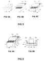
FIGS. 5 are bird's-eye views each illustrating a manufacturing process according to the present invention. -
FIGS. 6 are views each illustrating the basic structure and a manufacturing process thereof according to the present invention.FIG. 6 (a) is a bird's-eye view, andFIG. 6(b) is a cross-sectional view taken along theline 6A-6B'. -
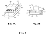
FIGS. 7 are views each illustrating the basic structure and the manufacturing process thereof according to the present invention.FIG. 7(a) is a bird's-eye view, andFIG. 7(b) is a cross-sectional view taken along theline 7A-7A'. -
- 001
- source region
- 002
- drain region
- 003
- gate electrode
- 004
- gate insulating film
- 005
- well region
- 006
- high resistance semiconductor substrate
- 007
- convex portion
- 008
- concave portion
- 019
- current path
- A first embodiment of the present invention is described with reference to
FIGS. 1 and 2 . -
FIG. 1(a) is a bird's-eye view,FIG. 1(b) is a plan view, andFIGS. 2(a), 2(b), and 2(c) are cross-sectional views taken along thelines 2A-2A', 2B-2B', and 2C-2C' ofFIG. 1(b) , respectively. InFIGS. 1 and 2 , components corresponding to those of the prior art illustrated inFIGS. 3 and 4 are denoted by the same reference symbols. It should be noted inFIG. 1(b) that, for simplicity of the figure, agate electrode 003 and agate insulating film 004 are transparent outside of trenches, and edges of thegate electrode 003 are indicated by thick lines. The first embodiment is different from the prior art in that a distance dp from a surface of a semiconductor substrate to a surface of the gate electrode embedded inside the trench is made larger in order to form asource region 001 and adrain region 002 as deep as possible below a concave portion of the trench. As illustrated inFIGS. 2 (b) and 2(c) , in a structure having a large distance dp, when the source/drain regions are formed by a multi-direction oblique ion implantation method, the ions enter side wall portions of the trench having the distance dp. As a result, the source/drain regions may be formed to a deeper part than in the prior art, and depths of the source/drain regions may be made up to as deep as dSD that is substantially the same depth as the distance dp. Accordingly, as illustrated inFIG. 1(a) , a larger current is allowed to flow along acurrent path 019 in a bottom part region of the trench compared with the prior art, and hence a driving performance is enhanced. -
FIGS. 5 each illustrate a method of manufacturing a lateral trench gate transistor having the above-mentionedstructure. First, as illustrated inFIG. 5(a) , a p-type well 005 is formed in an n-type or p-type semiconductor substrate 006, and then a trench having aconvex portion 007 and aconcave portion 008 is formed (normally, apluralityof trenches are formed). Next, as illustrated inFIG. 5(b) , an oxide film having a predetermined film thickness is grown by thermal oxidation to form thegate insulating film 004. Subsequently, for example, Poly-Si is deposited for the formation of thegate electrode 003. After that, a predetermined part of the Poly-Si is masked by a resist, and the other part of the Poly-Si is etched. In the etching, the Poly-Si is etched to such an extent that the oxide film in the source/drain regions does not disappear due to etching loss while the Poly-Si embedded inside the trench is removed as much as possible, to thereby increase the distance dP. More specifically, the gate electrode includes: a second gate electrode formed on the surface of the semiconductor substrate; a first gate electrode that is locatedbelow the second gate electrode and embedded inside the trench; and a third gate electrode that is formed on both sides of the first gate electrode inside the trench and has a surface to be etched. After that, as illustrated inFIG. 5(c) , n-type ionic species are implanted, and the source/drain regions (001 and 002) are formed by self-alignment. In this case, by implanting ions using the multi-direction oblique ion implantation method, the ions are implanted into side walls of the trench on which the gate electrode is not formed. As a result, the source/drain regions may be formed to a deeper part than in the prior art. - When the depths of the source/drain regions are made equal to a height of the bottom part of the trench, the driving performance is most enhanced. As illustrated in
FIGS. 6(a) and 6(b) , this may be realized by completely removing a part of the gate electrode inside the trench, the part being not masked in the above-mentioned etching of the gate electrode. However, there may be a case where, depending on a depth of the trench, a thickness of the gate oxide film, and an etching selectivity of the gate electrode to the oxide film, the oxide film in the source/drain regions disappear due to etching loss before the gate electrode inside the trench is completely removed, the etching reaches the silicon in the source/drain regions, and a shape as illustrated inFIGS. 7 (a) and 7 (b) is obtained. However, even with this shape, by implanting n-type ionic species using the multi-direction oblique ion implantation method similarly to the above, the source/drain regions may be formed to a still deeper part. As a result, the formed transistor functions as a high driving performance MOS. - In the above-mentioned embodiment, it is needless to say that a p-channel MOS structure may also be made in the same manner by reversing conductivity types. The use of a twin well technology easily enables making a CMOS structure having a high driving performance in one chip and also integrally mounting an IC. The above description is given on the basic structure and the basic manufacturing method according to the present invention.
- Now, a description will be given to the application of the basic structure.
- In ordinary planar MOS transistors, various structures exist aiming to improve the withstanding voltage based on a basic structure. In the present invention, an improvement of withstanding voltage may be attained easily by combining conventional art of the LDD (light doped drain) structure, the DDD (double diffused drain) structure, the LDMOS (lateral double diffusedMOS) structure, or the like to the basic structure (
FIGS. 5 to 7 ). - Also, the width of the
convex portion 007 illustrated inFIG. 1 is about 1,000 Å whereby the inner part of the convex portion is fully depleted when the MOS transistor is in the ON state, and the sub-threshold characteristic is improved. Accordingly, leak current between the source and the drain is reduced, the threshold maybe lowered, and the drivingperformance maybe resultantly further improved. - Further, when the present invention and the conventional twin well technology are adopted in combination, it becomes possible to integrally mount a semiconductor device with a bipolar channel according to the present invention and a normal IC on the same chip, which enables easily making an IC with which a CMOS driver is integrally mounted.
- The embodiment of the present invention has been described, but the present invention is not limited to the above embodiment and may be modified within a range that does not depart from the gist of the invention.
Claims (11)
- A semiconductor device, comprising:a well region which is formed of a high resistance first conductivity type semiconductor at a predetermined depth from a surface of a semiconductor substrate;a plurality of trenches which extend from a surface to a midway depth of the well region;a gate insulating film which is formed on surfaces of a concave portion and a convex portion formed by each of the trenches;a first gate electrode which is embedded inside the trenches;a second gate electrode which is formed on the surface of the semiconductor substrate in contact with the first gate electrode in regions of the concave portion and the convex portion, the regions excluding vicinities of both ends of the trenches;a third gate electrode which is embedded inside the trenches in the vicinities of the both ends of the trenches in contact with the first gate electrode and the second gate electrode so that a surface of the third gate electrode is located at a position deeper than the surface of the semiconductor substrate; anda source region and a drain region which are formed as low resistance second conductivity type semiconductor layers from a part of the semiconductor surface, the part being out of contact with the third gate electrode, so as to be deeper in a side surface of the concave portion of each of the trenches than in the surface of the convex portion of each of the trenches and shallower than the depth of the well region.
- A semiconductor device according to claim 1, wherein the third gate electrode is omitted.
- A semiconductor device according to claim 2, wherein the source region and the drain region each have an upper surface which is located at a position lower than an uppermost surface of the gate insulating film.
- A semiconductor device according to any one of claims 1 to 3, wherein the source region and the drain region each have a light doped drain (LDD) structure.
- A semiconductor device according to any one of claims 1 to 3, wherein the source region and the drain region each have a double diffused drain (DDD) structure.
- A semiconductor device according to any one of claims 1 to 3, wherein the source region and the drain region each have a lateral double diffused metal oxide semiconductor (LDMOS) structure.
- A semiconductor device according to any one of claims 1 to 3, wherein a width of the convex portion of the trench portion is approximately 1,000 Å.
- A semiconductor device according to any one of claims 1 to 3, wherein the semiconductor device is combined with a twin well technique.
- A semiconductor device according to any one of claims 1 to 3, wherein all the conductivity types are reversed.
- A method of manufacturing a semiconductor device, comprising:forming a well region of a high resistance first conductivity type semiconductor at a predetermined depth from a surface of a semiconductor substrate;forming a plurality of trenches which extend from a surface to a midway depth of the well region;forming a gate insulating film on surfaces of a concave portion and a convex portion formed by each of the trenches;depositing a gate electrode material inside the trenches and on the surface of the semiconductor substrate;etching the gate electrode material to form:a first gate electrode which is embedded inside the trenches;a second gate electrode which is formed on the surface of the semiconductor substrate in contact with the first gate electrode in regions of the concave portion and the convex portion, the regions excluding vicinities of both ends of the trenches; anda third gate electrode which is embedded inside the trenches in the vicinities of the both ends of the trenches in contact with the first gate electrode and the second gate electrode so that a surface of the third gate electrode is located at a position deeper than the surface of the semiconductor substrate; andforming, by a multi-direction oblique ion implantation method, a source region and a drain region as low resistance second conductivity type semiconductor layers from a part of the semiconductor surface, the part being out of contact with the third gate electrode, so as to be deeper in a side surface of the concave portion of each of the trenches than in the surface of the convex portion of each of the trenches and shallower than the depth of the well region.
- A method of manufacturing a semiconductor device according to claim 10, further comprising etching the semiconductor surface in the source region and the drain region at the same time as the etching the gate electrode material.
Applications Claiming Priority (2)
| Application Number | Priority Date | Filing Date | Title |
|---|---|---|---|
| JP2007220964A JP5258230B2 (en) | 2007-08-28 | 2007-08-28 | Manufacturing method of semiconductor device |
| PCT/JP2008/064853 WO2009028375A1 (en) | 2007-08-28 | 2008-08-20 | Semiconductor device and method for manufacturing the same |
Publications (2)
| Publication Number | Publication Date |
|---|---|
| EP2187431A1 true EP2187431A1 (en) | 2010-05-19 |
| EP2187431A4 EP2187431A4 (en) | 2012-02-15 |
Family
ID=40387098
Family Applications (1)
| Application Number | Title | Priority Date | Filing Date |
|---|---|---|---|
| EP08792574A Ceased EP2187431A4 (en) | 2007-08-28 | 2008-08-20 | SEMICONDUCTOR DEVICE AND METHOD FOR MANUFACTURING THE SAME |
Country Status (7)
| Country | Link |
|---|---|
| US (1) | US8390061B2 (en) |
| EP (1) | EP2187431A4 (en) |
| JP (1) | JP5258230B2 (en) |
| KR (2) | KR101635648B1 (en) |
| CN (1) | CN101796620B (en) |
| TW (1) | TWI445171B (en) |
| WO (1) | WO2009028375A1 (en) |
Cited By (1)
| Publication number | Priority date | Publication date | Assignee | Title |
|---|---|---|---|---|
| FR2995139A1 (en) * | 2012-09-04 | 2014-03-07 | St Microelectronics Sa | TRANSISTOR MOS |
Families Citing this family (3)
| Publication number | Priority date | Publication date | Assignee | Title |
|---|---|---|---|---|
| CN105097916A (en) * | 2014-05-05 | 2015-11-25 | 中芯国际集成电路制造(上海)有限公司 | Mos transistor device and manufacturing method thereof |
| US10199475B2 (en) | 2016-05-24 | 2019-02-05 | Maxim Integrated Products, Inc. | LDMOS transistors and associated systems and methods |
| CN109065635B (en) * | 2018-08-22 | 2021-05-14 | 电子科技大学 | Transverse diode device |
Family Cites Families (10)
| Publication number | Priority date | Publication date | Assignee | Title |
|---|---|---|---|---|
| US223253A (en) * | 1880-01-06 | Half op his eight to geoege joseph o doheett | ||
| US101110A (en) * | 1870-03-22 | Improvement in drop-wire supporting-bars or plates of warfing-machines | ||
| EP0203146B1 (en) | 1984-11-27 | 1989-05-24 | AT&T Corp. | Trench transistor |
| JPH0575121A (en) * | 1991-09-18 | 1993-03-26 | Fujitsu Ltd | Semiconductor device |
| US5399516A (en) * | 1992-03-12 | 1995-03-21 | International Business Machines Corporation | Method of making shadow RAM cell having a shallow trench EEPROM |
| US5467305A (en) * | 1992-03-12 | 1995-11-14 | International Business Machines Corporation | Three-dimensional direct-write EEPROM arrays and fabrication methods |
| US5932911A (en) * | 1996-12-13 | 1999-08-03 | Advanced Micro Devices, Inc. | Bar field effect transistor |
| JP2001102574A (en) * | 1999-09-29 | 2001-04-13 | Toshiba Corp | Semiconductor device with trench gate |
| JP2006019518A (en) * | 2004-07-01 | 2006-01-19 | Seiko Instruments Inc | Horizontal trench MOSFET |
| JP4976658B2 (en) | 2005-04-05 | 2012-07-18 | セイコーインスツル株式会社 | Manufacturing method of semiconductor device |
-
2007
- 2007-08-28 JP JP2007220964A patent/JP5258230B2/en not_active Expired - Fee Related
-
2008
- 2008-08-20 US US12/733,191 patent/US8390061B2/en not_active Expired - Fee Related
- 2008-08-20 WO PCT/JP2008/064853 patent/WO2009028375A1/en not_active Ceased
- 2008-08-20 CN CN200880106197XA patent/CN101796620B/en not_active Expired - Fee Related
- 2008-08-20 EP EP08792574A patent/EP2187431A4/en not_active Ceased
- 2008-08-20 KR KR1020107004473A patent/KR101635648B1/en not_active Expired - Fee Related
- 2008-08-20 KR KR1020167016896A patent/KR101747615B1/en not_active Expired - Fee Related
- 2008-08-26 TW TW097132551A patent/TWI445171B/en not_active IP Right Cessation
Cited By (2)
| Publication number | Priority date | Publication date | Assignee | Title |
|---|---|---|---|---|
| FR2995139A1 (en) * | 2012-09-04 | 2014-03-07 | St Microelectronics Sa | TRANSISTOR MOS |
| US9012957B2 (en) | 2012-09-04 | 2015-04-21 | Stmicroelectronics S.A. | MOS transistor |
Also Published As
| Publication number | Publication date |
|---|---|
| KR101635648B1 (en) | 2016-07-01 |
| CN101796620B (en) | 2013-03-27 |
| CN101796620A (en) | 2010-08-04 |
| EP2187431A4 (en) | 2012-02-15 |
| US20100289078A1 (en) | 2010-11-18 |
| JP5258230B2 (en) | 2013-08-07 |
| TW200931665A (en) | 2009-07-16 |
| JP2009054840A (en) | 2009-03-12 |
| WO2009028375A1 (en) | 2009-03-05 |
| KR20100065152A (en) | 2010-06-15 |
| US8390061B2 (en) | 2013-03-05 |
| KR101747615B1 (en) | 2017-06-14 |
| KR20160075873A (en) | 2016-06-29 |
| TWI445171B (en) | 2014-07-11 |
Similar Documents
| Publication | Publication Date | Title |
|---|---|---|
| JP2010278312A (en) | Semiconductor device | |
| JP4976658B2 (en) | Manufacturing method of semiconductor device | |
| KR101152451B1 (en) | Lateral semiconductor device using trench structure and method of manufacturing the same | |
| JP2006019518A (en) | Horizontal trench MOSFET | |
| JP6298307B2 (en) | Semiconductor memory device and manufacturing method thereof | |
| KR100390614B1 (en) | Semiconductor device and method of manufacturing the same | |
| KR101667499B1 (en) | Semiconductor device and method of manufacturing the same | |
| JP5486654B2 (en) | Semiconductor device | |
| US8390061B2 (en) | Semiconductor device having a trench structure and method for manufacturing the same | |
| KR20090092718A (en) | Semiconductor device and method of manufacturing the same | |
| US7256086B2 (en) | Trench lateral power MOSFET and a method of manufacturing the same | |
| JP2009049260A (en) | Lateral high drive capability semiconductor device using trench structure | |
| JP5486673B2 (en) | Semiconductor device | |
| JP2001102574A (en) | Semiconductor device with trench gate | |
| JP2008053468A (en) | Lateral high drive capability semiconductor device using trench structure | |
| JP2012004471A (en) | Semiconductor device and method of manufacturing the same |
Legal Events
| Date | Code | Title | Description |
|---|---|---|---|
| PUAI | Public reference made under article 153(3) epc to a published international application that has entered the european phase |
Free format text: ORIGINAL CODE: 0009012 |
|
| 17P | Request for examination filed |
Effective date: 20100329 |
|
| AK | Designated contracting states |
Kind code of ref document: A1 Designated state(s): AT BE BG CH CY CZ DE DK EE ES FI FR GB GR HR HU IE IS IT LI LT LU LV MC MT NL NO PL PT RO SE SI SK TR |
|
| AX | Request for extension of the european patent |
Extension state: AL BA MK RS |
|
| DAX | Request for extension of the european patent (deleted) | ||
| A4 | Supplementary search report drawn up and despatched |
Effective date: 20120112 |
|
| RIC1 | Information provided on ipc code assigned before grant |
Ipc: H01L 21/336 20060101AFI20120106BHEP Ipc: H01L 29/423 20060101ALI20120106BHEP Ipc: H01L 29/78 20060101ALI20120106BHEP |
|
| 17Q | First examination report despatched |
Effective date: 20130410 |
|
| RAP1 | Party data changed (applicant data changed or rights of an application transferred) |
Owner name: SII SEMICONDUCTOR CORPORATION |
|
| REG | Reference to a national code |
Ref country code: DE Ref legal event code: R003 |
|
| STAA | Information on the status of an ep patent application or granted ep patent |
Free format text: STATUS: THE APPLICATION HAS BEEN REFUSED |
|
| 18R | Application refused |
Effective date: 20161210 |