EP2182335A2 - PDM Output Temperature Sensor - Google Patents

PDM Output Temperature Sensor Download PDF

Info

Publication number
EP2182335A2
EP2182335A2 EP09174245A EP09174245A EP2182335A2 EP 2182335 A2 EP2182335 A2 EP 2182335A2 EP 09174245 A EP09174245 A EP 09174245A EP 09174245 A EP09174245 A EP 09174245A EP 2182335 A2 EP2182335 A2 EP 2182335A2
Authority
EP
European Patent Office
Prior art keywords
switch
node
signal
capacitor
voltage
Prior art date
Legal status (The legal status is an assumption and is not a legal conclusion. Google has not performed a legal analysis and makes no representation as to the accuracy of the status listed.)
Withdrawn
Application number
EP09174245A
Other languages
German (de)
French (fr)
Other versions
EP2182335A3 (en
Inventor
Ryoichi Anzai
Current Assignee (The listed assignees may be inaccurate. Google has not performed a legal analysis and makes no representation or warranty as to the accuracy of the list.)
Seiko Instruments Inc
Original Assignee
Seiko Instruments Inc
Priority date (The priority date is an assumption and is not a legal conclusion. Google has not performed a legal analysis and makes no representation as to the accuracy of the date listed.)
Filing date
Publication date
Application filed by Seiko Instruments Inc filed Critical Seiko Instruments Inc
Publication of EP2182335A2 publication Critical patent/EP2182335A2/en
Publication of EP2182335A3 publication Critical patent/EP2182335A3/en
Withdrawn legal-status Critical Current

Links

Images

Classifications

    • GPHYSICS
    • G01MEASURING; TESTING
    • G01KMEASURING TEMPERATURE; MEASURING QUANTITY OF HEAT; THERMALLY-SENSITIVE ELEMENTS NOT OTHERWISE PROVIDED FOR
    • G01K7/00Measuring temperature based on the use of electric or magnetic elements directly sensitive to heat ; Power supply therefor, e.g. using thermoelectric elements
    • G01K7/02Measuring temperature based on the use of electric or magnetic elements directly sensitive to heat ; Power supply therefor, e.g. using thermoelectric elements using thermoelectric elements, e.g. thermocouples
    • G01K7/14Arrangements for modifying the output characteristic, e.g. linearising
    • GPHYSICS
    • G01MEASURING; TESTING
    • G01KMEASURING TEMPERATURE; MEASURING QUANTITY OF HEAT; THERMALLY-SENSITIVE ELEMENTS NOT OTHERWISE PROVIDED FOR
    • G01K7/00Measuring temperature based on the use of electric or magnetic elements directly sensitive to heat ; Power supply therefor, e.g. using thermoelectric elements
    • G01K7/01Measuring temperature based on the use of electric or magnetic elements directly sensitive to heat ; Power supply therefor, e.g. using thermoelectric elements using semiconducting elements having PN junctions
    • GPHYSICS
    • G01MEASURING; TESTING
    • G01KMEASURING TEMPERATURE; MEASURING QUANTITY OF HEAT; THERMALLY-SENSITIVE ELEMENTS NOT OTHERWISE PROVIDED FOR
    • G01K7/00Measuring temperature based on the use of electric or magnetic elements directly sensitive to heat ; Power supply therefor, e.g. using thermoelectric elements
    • GPHYSICS
    • G01MEASURING; TESTING
    • G01KMEASURING TEMPERATURE; MEASURING QUANTITY OF HEAT; THERMALLY-SENSITIVE ELEMENTS NOT OTHERWISE PROVIDED FOR
    • G01K2219/00Thermometers with dedicated analog to digital converters

Definitions

  • the present invention relates to a pulse density modulation (PDM) output temperature sensor.
  • PDM pulse density modulation
  • FIG. 11 is a block diagram illustrating a conventional temperature sensor.
  • the conventional temperature sensor includes a reference voltage circuit 102 that generates a bandgap reference voltage V REF , a temperature detection circuit 106 that corrects a temperature dependent voltage to generate a voltage V CORR , a circuit 108 that outputs a reference voltage V HREF based on the bandgap reference voltage V REF and the voltage V CORR , a circuit 110 that multiplies the reference voltage V HREF by a factor (1/C) to output a reference voltage V 0 , a temperature detection circuit 104 that generates a temperature dependent voltage V TEMP , and an analog to digital converter (ADC) 112 that outputs a digital signal based on the reference voltage V 0 and the temperature dependent voltage V TEMP (see, for example, US 6,183,131 ).
  • ADC analog to digital converter
  • the conventional temperature sensor uses the reference voltage circuit 102. Accordingly, the conventional temperature sensor requires a larger area and consumes more power correspondingly.
  • the present invention has been made in view of the above, and an object of the present invention is therefore to provide a pulse density modulation (PDM) output temperature sensor that may be reduced in area and consumption power.
  • PDM pulse density modulation
  • the present invention provides a PDM output temperature sensor including: a first constant current source provided between a power supply terminal and a seventh node; a second constant current source provided between the power supply terminal and an eighth node; a first switch provided between the seventh node and a first node; a second switch provided between the seventh node and a fourth node; a third switch provided between the eighth node and the first node; a fourth switch provided between the eighth node and the fourth node; a first PNP bipolar transistor having a base and a collector connected to a ground terminal, and an emitter connected to the first node; a second PNP bipolar transistor having a base and a collector connected to the ground terminal, and an emitter connected to the fourth node; a fifth switch and a first capacitor provided between the first node and a second node in the stated order; an eighth switch provided between the second node and a third node; a sixth switch and a second capacitor provided between the first node and
  • the PDM output temperature sensor does not use the reference voltage circuit. Accordingly, the PDM output temperature sensor requires a smaller area and consumes less power correspondingly.
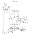
  • FIG. 1 is a block diagram illustrating the PDM output temperature sensor according to the first embodiment of the present invention.
  • the PDM output temperature sensor according to the first embodiment of the present invention includes a power supply terminal 45, a ground terminal 46, and an output terminal 47.
  • the PDM output temperature sensor according to the first embodiment of the present invention further includes nodes N1 to N8.
  • the PDM output temperature sensor includes constant current sources 11 and 12, PNP bipolar transistors (PNPs) 13 and 14, switches 15 to 18, switches 21 to 25, switches 31 to 35, capacitors 26 to 28, capacitors 36 to 38, an amplifier 41, a comparator 42, a latch 43, an inverter 44, and an oscillation circuit 51.
  • PNPs PNP bipolar transistors
  • the constant current source 11 is provided between the power supply terminal 45 and the node N7.
  • the constant current source 12 is provided between the power supply terminal 45 and the node N8.
  • the switch 15 is provided between the node N7 and the node N1.
  • the switch 16 is provided between the node N7 and the node N4.
  • the switch 17 is provided between the node N8 and the node N1.
  • the switch 18 is provided between the node N8 and the node N4.
  • the PNP 13 has a base and a collector connected to the ground terminal 46, and an emitter connected to the node N1.
  • the PNP 14 has a base and a collector connected to the ground terminal 46, and an emitter connected to the node N4.
  • the switch 21 and the capacitor 26 are provided between the node N1 and the node N2 in the stated order.
  • the switch 24 is provided between the node N2 and the node N3.
  • the switch 22 and the capacitor 27 are provided between the node N1 and the node N2 in the stated order.
  • the switch 25 and the capacitor 28 are provided between the node N2 and the node N3 in the stated order.
  • the switch 23 is provided between the ground terminal 46 and a connection point between the switch 22 and the capacitor 27.
  • the switch 31 and the capacitor 36 are provided between the node N4 and the node N5 in the stated order.
  • the switch 34 is provided between the node N5 and the node N6.
  • the switch 32 and the capacitor 37 are provided between the node N4 and the node N5 in the stated order.
  • the switch 35 and the capacitor 38 are provided between the node N5 and the node N6 in the stated order.
  • the switch 33 is provided between the ground terminal 46 and a connection point between the switch 32 and the capacitor 37.
  • the amplifier 41 has a non-inverting input terminal connected to the node N2, an inverting input terminal connected to the node N5, a non-inverting output terminal connected to the node N6, and an inverting output terminal connected to the node N3.
  • the comparator 42 has a non-inverting input terminal connected to the node N3, an inverting input terminal connected to the node N6, and an output terminal connected to an input terminal of the latch 43.
  • the latch 43 has an output terminal connected to an input terminal of the inverter 44.
  • the inverter 44 has an output terminal connected to the output terminal 47.
  • the oscillation circuit 51 transmits a signal ⁇ 1 to the switch 15, the switch 18, the switch 22, the switch 24, the switch 33, and the switch 34, the signal ⁇ 1 to the latch 43, and a signal ⁇ 2 to the switch 16, the switch 17, the switch 23, the switch 25, the switch 32, and the switch 35.
  • the latch 43 transmits a signal ⁇ XD to the switch 21 and the switch 31.
  • the inverter 44 transmits a signal ⁇ D to the switch 22, the switch 23, the switch 32, and the switch 33.
  • FIG. 2 is a graph illustrating changes in voltages Vbe1 and Vbe2 and differential voltage ⁇ Vbe based on the change in temperature.
  • the differential voltage ⁇ Vbe is a voltage obtained by subtracting the voltage Vbe1 from the voltage Vbe2(Vbe2-Vbe1).
  • Each of the voltages Vbe1 and Vbe2 has a negative temperature coefficient. With the constant current i2 being larger than the constant current i1, the voltage Vbe2 is higher than the voltage Vbe1, and the voltage Vbe2 has a gentler slope than the voltage Vbe1.
  • the differential voltage ⁇ Vbe has a positive temperature coefficient.
  • FIG. 3 is a time chart at the temperature Ta.
  • a signal ⁇ 1 ⁇ D is a signal obtained by a logical conjunction (AND) of the signal ⁇ 1 and the signal ⁇ D
  • a signal ⁇ 2 ⁇ D is a signal obtained by a logical conjunction (AND) of the signal ⁇ 2 and the signal ⁇ D.
  • VaN - ⁇ Vbe ⁇ C ⁇ 2 / C ⁇ 1 That is, the voltage VaN in an interval 2 is lower than the voltage VaN in the interval 6 by a value obtained by the expression (5).
  • the voltage VaN being a positive voltage with respect to a bias point and the voltage VaP being a negative voltage with respect to a bias point
  • the voltage Vc is high.
  • the PDM output temperature sensor operates as in the interval 1 in terms of the signals.
  • the PDM output temperature sensor operates so that, with the voltage Vbe1 being plus when the signal ⁇ D is high, the voltage VaN becomes higher than the bias point, the voltage VaP becomes lower than the bias point, and the voltage Vc becomes high.
  • the PDM output temperature sensor operates so that a voltage obtained by subtracting the voltage VaP from the voltage VaN at the input terminal of the comparator 42 becomes 0 V.
  • the PDM output temperature sensor changes from the ⁇ Vbe transfer mode in which the voltage VaN is set low and the voltage VaP is set high to a Vbe1 transfer mode in which the voltage VaN is set high and the voltage VaP is set low.
  • a voltage based on the voltage Vbe1 is added to the voltage VaN and the voltage based on the voltage Vbe1 is subtracted from the voltage VaP until the voltage Vc becomes high.
  • the rising edge of the signal ⁇ 1 causes the signal ⁇ XD to also become low (and the PDM output temperature sensor enters the Vbe1 transfer mode), and the inverter 44 causes the signal ⁇ D to become high. Therefore, the signal ⁇ 1 ⁇ D becomes high and the signal ⁇ 2 ⁇ D becomes low.
  • VaP - Vbe ⁇ 1 ⁇ C ⁇ 3 / C ⁇ 1 That is, the voltage VaP in the interval 6 is lower than the voltage VaP in the interval 4 by a value obtained by the expression (9a). With the voltage VaN being a positive voltage with respect to a bias point and the voltage VaP being a negative voltage with respect to a bias point, the voltage Vc is high. Note that with the voltage Vc being low in the interval 4, the rising edge of the signal ⁇ 1 causes the signal ⁇ XD to also become low (and the PDM output temperature sensor enters the Vbe1 transfer mode), and the inverter 44 causes the signal ⁇ D to become high. Therefore, the signal ⁇ 1 ⁇ D becomes low and the signal ⁇ 2. ⁇ D becomes high.
  • the PDM output temperature sensor operates so that, with the differential voltage ⁇ Vbe being minus when the signal ⁇ D is low, the voltage VaN becomes lower than the bias point, the voltage VaP becomes higher than the bias point, and the voltage Vc becomes low.
  • the PDM output temperature sensor operates so that the voltage obtained by subtracting the voltage VaP from the voltage VaN at the input terminal of the comparator 42 becomes 0 V.
  • the PDM output temperature sensor changes from the Vbe1 transfer mode in which the voltage VaN is set high and the voltage VaP is set low to the ⁇ Vbe transfer mode in which the voltage VaN is set low and the voltage VaP is set high.
  • the ⁇ Vbe transfer mode a voltage based on the differential voltage ⁇ Vbe is subtracted from the voltage VaN and the voltage based on the differential voltage ⁇ Vbe is added to the voltage VaP until the voltage Vc becomes low.
  • switches 15 to 18 cause the voltage VbeB to transition oppositely to the voltage VbeA.
  • the switches 21 to 25 and the switches 31 to 35 cause the voltage VaP to transition oppositely to the voltage VaN.
  • the differential voltage ⁇ Vbe at the temperature Tb is higher than the differential voltage ⁇ Vbe at the temperature Ta as illustrated in FIG. 2 . That is, the voltage VaN becomes low faster. Therefore, while it takes two cycles of the signal ⁇ 1 for the voltage VaN to be a negative voltage with respect to the bias point at the temperature Ta, it takes only one cycle of the signal ⁇ 1 at the temperature Tb. The same holds true for the voltage VaP.
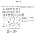
  • FIG. 5 is a time chart at the temperature Tc.
  • the voltage Vbe1 at the temperature Tc is lower than the voltage Vbe1 at the temperature Tb as illustrated in FIG. 2 . That is, the voltage VaN becomes high slower. Therefore, while it takes only one cycle of the signal ⁇ 1 for the voltage VaN to be a positive voltage with respect to the bias point at the temperature Tb, it takes two cycles of the signal ⁇ 1 at the temperature Tc. The same holds true for the voltage VaP.
  • the PDM output temperature sensor of the first embodiment of the present invention does not use a reference voltage circuit. Accordingly, the PDM output temperature sensor is reduced in area and consumption power correspondingly.
  • the amplifier 41 and the comparator 42 do not operate based on the reference voltage and hence are independent of fluctuation in reference voltage.
  • the first embodiment of the present invention compared with a third embodiment of the present invention, fewer switches are provided between the node N1 and the node N2. Therefore, switching noise to the capacitor 27 is reduced, and precision of the voltage VaN is improved. The same holds true for the voltage VaP.
  • FIG. 6 is a block diagram illustrating the PDM output temperature sensor according to the second embodiment of the present invention.
  • the PDM output temperature sensor according to the second embodiment of the present invention has the same circuit structure as the PDM output temperature sensor according to the first embodiment of the present invention.
  • the PDM output temperature sensor according to the second embodiment of the present invention is different from the PDM output temperature sensor according to the first embodiment of the present invention in that the switch 22 is controlled by a signal ⁇ XD+ ⁇ 1 ⁇ D and the switch 32 is controlled by a signal ⁇ XD+ ⁇ 2 ⁇ D.
  • the signal ⁇ XD+ ⁇ 1 ⁇ D is a signal obtained by a logical disjunction (OR) of the signal ⁇ XD and a signal obtained by a logical conjunction (AND) of the signal ⁇ 1 and the signal ⁇ D
  • the signal ⁇ XD+ ⁇ 2 ⁇ D is a signal obtained by a logical disjunction (OR) of the signal ⁇ XD and a signal obtained by a logical conjunction (AND) of the signal ⁇ 2 and the signal ⁇ D.
  • the latch 43 transmits the signal ⁇ XD to the switch 21 and the switch 31, and transmits the signal ⁇ XD also to the switch 22 and the switch 32.
  • FIG. 7 is a time chart at the temperature Ta according to the second embodiment of the present invention.
  • FIG. 8 is a time chart at the temperature Tb according to the second embodiment of the present invention.
  • FIG. 9 is a time chart at the temperature Tc according to the second embodiment of the present invention.
  • a capacitance value of the input capacitance is the capacitance value C2 of the capacitor 26.
  • the voltage VaN is reduced by a voltage ( ⁇ Vbe ⁇ C2/C1) in one cycle of the signal ⁇ 1 based on the capacitance value C2.
  • the capacitance value of the input capacitance increases from the capacitance value C2 of the capacitor 26 to a total capacitance value (C2+C3) of the capacitors 26 and 27.
  • the voltage VaN is reduced by a voltage ( ⁇ Vbe ⁇ (C2+C3)/C1) in one cycle of the signal ⁇ 1 based on the capacitance value (C2+C3). The same holds true for the capacitor 36.
  • the PDM output temperature sensor of the second embodiment of the present invention when the PDM output temperature sensor enters the ⁇ Vbe transfer mode, not only the capacitor 26 but both the capacitors 26 and 27 operate as the input capacitance. Therefore, the capacitance value of the input capacitance increases from the capacitance value C2 of the capacitor 26 to the total capacitance value (C2+C3) of the capacitors 26 and 27. Accordingly, the capacitance value C2 of the capacitor 26 does not need to be high.
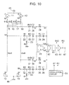
  • FIG. 10 is a block diagram illustrating the PDM output temperature sensor according to the third embodiment of the present invention.
  • a switch 53 and a switch 63 are added when compared with the first embodiment of the present invention.
  • the switch 22, the switch 53, and the capacitor 27 are provided between the node N1 and the node N2 in the stated order.
  • the oscillation circuit 51 transmits a signal ⁇ 1 to the switch 15, the switch 18, the switch 22, the switch 24, the switch 33, and the switch 34, the signal ⁇ 1 to the latch 43, and a signal ⁇ 2 to the switch 16, the switch 17, the switch 23, the switch 25, the switch 32, and the switch 35.
  • the latch 43 transmits a signal ⁇ XD to the switch 21 and the switch 31.
  • the inverter 44 transmits a signal ⁇ D to the switch 53 and the switch 63.
  • the switch 22 when the signal ⁇ 1 and the signal ⁇ D become high, the switch 22 is turned ON to connect the node N1 to the capacitor 27.
  • the switch 22 and the switch 53 when the signal ⁇ 1 and the signal ⁇ D become high, the switch 22 and the switch 53 are turned ON to connect the node N1 to the capacitor 27.
  • the switch 23 when the signal ⁇ 2 and the signal ⁇ D become high, the switch 23 is turned ON to connect the ground terminal 46 to the capacitor 27.
  • the switch 23 and the switch 53 when the signal ⁇ 2 and the signal ⁇ D become high, the switch 23 and the switch 53 are turned ON to connect the ground terminal 46 to the capacitor 27.
  • the switch 32 when the signal ⁇ 2 and the signal ⁇ D become high, the switch 32 is turned ON to connect the node N4 to the capacitor 37.
  • the switch 32 and the switch 63 when the signal ⁇ 2 and the signal ⁇ D become high, the switch 32 and the switch 63 are turned ON to connect the node N4 to the capacitor 37.
  • the switch 33 when the signal ⁇ 1 and the signal ⁇ D become high, the switch 33 is turned ON to connect the ground terminal 46 to the capacitor 37.
  • the switch 33 and the switch 63 when the signal ⁇ 1 and the signal ⁇ D become high, the switch 33 and the switch 63 are turned ON to connect the ground terminal 46 to the capacitor 37.
  • the PDM output temperature sensor according to the third embodiment of the present invention operates as in the first embodiment of the present invention.
  • the switches and the signals for controlling the switches have a one-to-one correspondence. Therefore, the control circuit for controlling the switches is simplified.

Landscapes

  • Physics & Mathematics (AREA)
  • General Physics & Mathematics (AREA)
  • Measuring Temperature Or Quantity Of Heat (AREA)
  • Amplifiers (AREA)
  • Measurement Of Current Or Voltage (AREA)
  • Analogue/Digital Conversion (AREA)

Abstract

To provide a PDM output temperature sensor, which is reduced in area and consumption power, provided is a PDM output temperature sensor which includes no reference voltage circuit, thereby having a smaller area and consuming less power correspondingly.

Description

  • The present invention relates to a pulse density modulation (PDM) output temperature sensor.
  • Currently, a temperature sensor that outputs a digital signal based on a temperature is included in a variety of electronic devices. FIG. 11 is a block diagram illustrating a conventional temperature sensor.
  • The conventional temperature sensor includes a reference voltage circuit 102 that generates a bandgap reference voltage VREF, a temperature detection circuit 106 that corrects a temperature dependent voltage to generate a voltage VCORR, a circuit 108 that outputs a reference voltage VHREF based on the bandgap reference voltage VREF and the voltage VCORR, a circuit 110 that multiplies the reference voltage VHREF by a factor (1/C) to output a reference voltage V0, a temperature detection circuit 104 that generates a temperature dependent voltage VTEMP, and an analog to digital converter (ADC) 112 that outputs a digital signal based on the reference voltage V0 and the temperature dependent voltage VTEMP (see, for example, US 6,183,131 ).
  • However, the conventional temperature sensor uses the reference voltage circuit 102. Accordingly, the conventional temperature sensor requires a larger area and consumes more power correspondingly.
  • The present invention has been made in view of the above, and an object of the present invention is therefore to provide a pulse density modulation (PDM) output temperature sensor that may be reduced in area and consumption power.
  • In order to solve the above-mentioned problem, the present invention provides a PDM output temperature sensor including: a first constant current source provided between a power supply terminal and a seventh node; a second constant current source provided between the power supply terminal and an eighth node; a first switch provided between the seventh node and a first node; a second switch provided between the seventh node and a fourth node; a third switch provided between the eighth node and the first node; a fourth switch provided between the eighth node and the fourth node; a first PNP bipolar transistor having a base and a collector connected to a ground terminal, and an emitter connected to the first node; a second PNP bipolar transistor having a base and a collector connected to the ground terminal, and an emitter connected to the fourth node; a fifth switch and a first capacitor provided between the first node and a second node in the stated order; an eighth switch provided between the second node and a third node; a sixth switch and a second capacitor provided between the first node and the second node in the stated order; a ninth switch and a third capacitor provided between the second node and the third node in the stated order; a seventh switch provided between the ground terminal and a connection point between the sixth switch and the second capacitor; a tenth switch and a fourth capacitor provided between the fourth node and a fifth node in the stated order; a thirteenth switch provided between the fifth node and a sixth node; an eleventh switch and a fifth capacitor provided between the fourth node and the fifth node in the stated order; a fourteenth switch and a sixth capacitor provided between the fifth node and the sixth node in the stated order; a twelfth switch provided between the ground terminal and a connection point between the eleventh switch and the fifth capacitor; an amplifier having a non-inverting input terminal connected to the second node, an inverting input terminal connected to the fifth node, a non-inverting output terminal connected to the sixth node, and an inverting output terminal connected to the third node; a comparator having a non-inverting input terminal connected to the third node, and an inverting input terminal connected to the sixth node; a latch having an input terminal connected to an output terminal of the comparator; an inverter having an input terminal connected to an output terminal of the latch, and an output terminal connected to an output terminal of the PDM output temperature sensor; and an oscillation circuit for controlling each of the first switch, the second switch, the third switch, the fourth switch, the sixth switch, the seventh switch, the eighth switch, the ninth switch, the eleventh switch, the twelfth switch, the thirteenth switch, the fourteenth switch, and the latch.
  • In order to solve the above-mentioned problem, the present invention provides a PDM output temperature sensor including: a first constant current source provided between a power supply terminal and a seventh node; a second constant current source provided between the power supply terminal and an eighth node; a first switch provided between the seventh node and a first node; a second switch provided between the seventh node and a fourth node; a third switch provided between the eighth node and the first node; a fourth switch provided between the eighth node and the fourth node; a first PNP bipolar transistor having a base and a collector connected to a ground terminal, and an emitter connected to the first node; a second PNP bipolar transistor having a base and a collector connected to the ground terminal, and an emitter connected to the fourth node; a fifth switch and a first capacitor provided between the first node and a second node in the stated order; an eighth switch provided between the second node and a third node; a sixth switch, a fifteenth switch, and a second capacitor provided between the first node and the second node in the stated order; a ninth switch and a third capacitor provided between the second node and the third node in the stated order; a seventh switch provided between the ground terminal and a connection point between the sixth switch and the second capacitor; a tenth switch and a fourth capacitor provided between the fourth node and a fifth node in the stated order; a thirteenth switch provided between the fifth node and a sixth node; an eleventh switch, a sixteenth switch, and a fifth capacitor provided between the fourth node and the fifth node in the stated order; a fourteenth switch and a sixth capacitor provided between the fifth node and the sixth node in the stated order; a twelfth switch provided between the ground terminal and a connection point between the eleventh switch and the fifth capacitor; an amplifier having a non-inverting input terminal connected to the second node, an inverting input terminal connected to the fifth node, a non-inverting output terminal connected to the sixth node, and an inverting output terminal connected to the third node; a comparator having a non-inverting input terminal connected to the third node, and an inverting input terminal connected to the sixth node; a latch having an input terminal connected to an output terminal of the comparator; an inverter having an input terminal connected to an output terminal of the latch, and an output terminal connected to an output terminal of the PDM output temperature sensor; and an oscillation circuit for controlling each of the first switch, the second switch, the third switch, the fourth switch, the sixth switch, the seventh switch, the eighth switch, the ninth switch, the eleventh switch, the twelfth switch, the thirteenth switch, the fourteenth switch, and the latch.
  • According to the present invention, the PDM output temperature sensor does not use the reference voltage circuit. Accordingly, the PDM output temperature sensor requires a smaller area and consumes less power correspondingly.
  • Embodiments of the present invention will now be described by way of further example only and with reference to the accompanying drawings, in which:
    • FIG. 1 is a block diagram illustrating a PDM output temperature sensor according to a first embodiment of the present invention;
    • FIG. 2 is a graph illustrating changes in voltages Vbe1 and Vbe2 and differential voltage ΔVbe in accordance with a change in temperature, of the PDM output temperature sensor according to the first embodiment of the present invention;
    • FIG. 3 is a time chart at a temperature Ta of the PDM output temperature sensor according to the first embodiment of the present invention;
    • FIG. 4 is a time chart at a temperature Tb of the PDM output temperature sensor according to the first embodiment of the present invention;
    • FIG. 5 is a time chart at a temperature Tc of the PDM output temperature sensor according to the first embodiment of the present invention;
    • FIG. 6 is a block diagram illustrating a PDM output temperature sensor according to a second embodiment of the present invention;
    • FIG. 7 is a time chart at the temperature Ta of the PDM output temperature sensor according to the second embodiment of the present invention;
    • FIG. 8 is a time chart at the temperature Tb of the PDM output temperature sensor according to the second embodiment of the present invention;
    • FIG. 9 is a time chart at the temperature Tc of the PDM output temperature sensor according to the second embodiment of the present invention;
    • FIG. 10 is a block diagram illustrating a PDM output temperature sensor according to a third embodiment of the present invention; and
    • FIG. 11 is a block diagram illustrating a conventional temperature sensor.
  • Hereinafter, embodiments of the present invention are described with reference to the drawings.
  • <First embodiment>
  • First, a structure of a pulse density modulation (PDM) output temperature sensor according to a first embodiment of the present invention is described. FIG. 1 is a block diagram illustrating the PDM output temperature sensor according to the first embodiment of the present invention.
  • The PDM output temperature sensor according to the first embodiment of the present invention includes a power supply terminal 45, a ground terminal 46, and an output terminal 47. The PDM output temperature sensor according to the first embodiment of the present invention further includes nodes N1 to N8.
  • The PDM output temperature sensor according to the first embodiment of the present invention includes constant current sources 11 and 12, PNP bipolar transistors (PNPs) 13 and 14, switches 15 to 18, switches 21 to 25, switches 31 to 35, capacitors 26 to 28, capacitors 36 to 38, an amplifier 41, a comparator 42, a latch 43, an inverter 44, and an oscillation circuit 51.
  • The constant current source 11 is provided between the power supply terminal 45 and the node N7. The constant current source 12 is provided between the power supply terminal 45 and the node N8. The switch 15 is provided between the node N7 and the node N1. The switch 16 is provided between the node N7 and the node N4. The switch 17 is provided between the node N8 and the node N1. The switch 18 is provided between the node N8 and the node N4. The PNP 13 has a base and a collector connected to the ground terminal 46, and an emitter connected to the node N1. The PNP 14 has a base and a collector connected to the ground terminal 46, and an emitter connected to the node N4.
  • The switch 21 and the capacitor 26 are provided between the node N1 and the node N2 in the stated order. The switch 24 is provided between the node N2 and the node N3. The switch 22 and the capacitor 27 are provided between the node N1 and the node N2 in the stated order. The switch 25 and the capacitor 28 are provided between the node N2 and the node N3 in the stated order. The switch 23 is provided between the ground terminal 46 and a connection point between the switch 22 and the capacitor 27.
  • The switch 31 and the capacitor 36 are provided between the node N4 and the node N5 in the stated order. The switch 34 is provided between the node N5 and the node N6. The switch 32 and the capacitor 37 are provided between the node N4 and the node N5 in the stated order. The switch 35 and the capacitor 38 are provided between the node N5 and the node N6 in the stated order. The switch 33 is provided between the ground terminal 46 and a connection point between the switch 32 and the capacitor 37.
  • The amplifier 41 has a non-inverting input terminal connected to the node N2, an inverting input terminal connected to the node N5, a non-inverting output terminal connected to the node N6, and an inverting output terminal connected to the node N3. The comparator 42 has a non-inverting input terminal connected to the node N3, an inverting input terminal connected to the node N6, and an output terminal connected to an input terminal of the latch 43. The latch 43 has an output terminal connected to an input terminal of the inverter 44. The inverter 44 has an output terminal connected to the output terminal 47.
  • The oscillation circuit 51 transmits a signal Φ1 to the switch 15, the switch 18, the switch 22, the switch 24, the switch 33, and the switch 34, the signal Φ1 to the latch 43, and a signal Φ2 to the switch 16, the switch 17, the switch 23, the switch 25, the switch 32, and the switch 35. The latch 43 transmits a signal ΦXD to the switch 21 and the switch 31. The inverter 44 transmits a signal ΦD to the switch 22, the switch 23, the switch 32, and the switch 33.
  • When each signal becomes high, the switches corresponding to the signal are turned ON. Also, when the signal Φ1 becomes high, the latch 43 stores and outputs a voltage Vc at the time point.
  • Next, changes in emitter voltages of the PNP 13 based on a change in temperature are described. FIG. 2 is a graph illustrating changes in voltages Vbe1 and Vbe2 and differential voltage ΔVbe based on the change in temperature.
  • When the PNP 13 allows a constant current i1 of the constant current source 11 to flow therethrough, the emitter of the PNP 13 generates the voltage Vbe1. When the PNP 13 allows a constant current i2 of the constant current source 12 to flow therethrough, the emitter of the PNP 13 generates the voltage Vbe2. The differential voltage ΔVbe is a voltage obtained by subtracting the voltage Vbe1 from the voltage Vbe2(Vbe2-Vbe1).
  • Each of the voltages Vbe1 and Vbe2 has a negative temperature coefficient. With the constant current i2 being larger than the constant current i1, the voltage Vbe2 is higher than the voltage Vbe1, and the voltage Vbe2 has a gentler slope than the voltage Vbe1. The differential voltage ΔVbe has a positive temperature coefficient.
  • The same holds true for the PNP 14.
  • Next, an operation of the PDM output temperature sensor at a temperature Ta, according to the first embodiment of the present invention is described. FIG. 3 is a time chart at the temperature Ta. Herein, a signal Φ1·ΦD is a signal obtained by a logical conjunction (AND) of the signal Φ1 and the signal ΦD, and a signal Φ2·ΦD is a signal obtained by a logical conjunction (AND) of the signal Φ2 and the signal ΦD.
  • [Operation in interval 1 (ΔVbe transfer mode)] When the signal Φ1 becomes high and the signal Φ2 becomes low, the constant current i1 is caused to flow through the PNP 13 to set the voltage VbeA to the voltage Vbe1, and the constant current i2 is caused to flow through the PNP 14 to set the voltage VbeB to the voltage Vbe2. Assume that the voltage across the node N2 is 0 V. Then, when a capacitance value of the capacitor 26 is C2, electric charges Q2 to be charged to the capacitor 26 are calculated as follows. Q 2 = C 2 Vbe 1 - 0 = C 2 Vbe 1
    Figure imgb0001

    At this time, only the capacitor 26 and the capacitor 36 are operating as input capacitance. Note that with the voltage Vc being high in an interval 6, the rising edge of the signal Φ1 causes the signal ΦXD to also become high (and the PDM output temperature sensor enters the ΔVbe transfer mode), and the inverter 44 causes the signal ΦD to become low. Therefore, the signal Φ1·ΦD and the signal Φ2·ΦD also become low.
  • [Operation in interval 2 (ΔVbe transfer mode)] When the signal Φ1 becomes low and the signal Φ2 becomes high, the constant current i2 is caused to flow through the PNP 13 to set the voltage VbeA to the voltage Vbe2, and the constant current i1 is caused to flow through the PNP 14 to set the voltage VbeB to the voltage Vbe1. Assume that the voltage across the node N2 is 0 V. Then, the electric charges Q2 to be charged to the capacitor 26 are calculated as follows. Q 2 = C 2 Vbe 2 - 0 = C 2 Vbe 2
    Figure imgb0002

    At this time, only the capacitor 26 and the capacitor 36 are operating as input capacitance. In this case, differential electric charges in the capacitor 26 are transferred to the capacitor 28. Assume that the voltage across the node N2 is 0 V. Then, when a voltage across the node N3 is VaN and a capacitance value of the capacitor 28 is C1, the electric charges Q1 to be charged to the capacitor 28 are calculated as follows. Q 1 = C 1 VaN - 0 = C 1 VaN
    Figure imgb0003

    Based on the equations (1) to (3), the following equation is satisfied. C 2 Vbe 1 - C 2 Vbe 2 = - C 2 ΔVbe = C 1 VaN
    Figure imgb0004

    Therefore, the following equation is satisfied. VaN = - ΔVbe C 2 / C 1
    Figure imgb0005

    That is, the voltage VaN in an interval 2 is lower than the voltage VaN in the interval 6 by a value obtained by the expression (5). In addition, a voltage VaP across the node N6, which transitions oppositely to the voltage VaN, is calculated as follows. VaP = ΔVbe C 2 / C 1
    Figure imgb0006

    That is, the voltage VaP in the interval 2 is higher than the voltage VaP in the interval 6 by a value obtained by the expression (5a). However, with the voltage VaN being a positive voltage with respect to a bias point and the voltage VaP being a negative voltage with respect to a bias point, the voltage Vc is high. Note that with the voltage Vc being high in the interval 6, the rising edge of the signal Φ1 causes the signal ΦXD to also become high (and the PDM output temperature sensor enters the ΔVbe transfer mode), and the inverter 44 causes the signal ΦD to become low. Therefore, the signal Φ1·ΦD and the signal Φ2·ΦD also become low.
  • [Operation in interval 3 (ΔVbe transfer mode)] The PDM output temperature sensor operates as in the interval 1 in terms of the signals.
  • [Operation in interval 4 (ΔVbe transfer mode)] The interval 2 and an interval 4 are the same in terms of the signal Φ1, the signal Φ2, the voltage VbeA, and the voltage VbeB. In addition, as in the interval 2, the equation (5) holds true. That is, the voltage VaN in the interval 4 is lower than the voltage VaN in the interval 2 by the value obtained by the equation (5). Further, as in the interval 2, the equation (5a) holds true. That is, the voltage VaP in the interval 4 is higher than the voltage VaP in the interval 2 by the value obtained by the equation (5a). In this case, with the voltage VaN being a negative voltage with respect to the bias point and the voltage VaP being a positive voltage with respect to the bias point, the voltage Vc is low. Note that with the voltage Vc being high in the interval 2, the rising edge of the signal Φ1 causes the signal ΦXD to also become high (and the PDM output temperature sensor enters the ΔVbe transfer mode), and the inverter 44 causes the signal ΦD to become low. Therefore, the signal Φ1·ΦD and the signal Φ2·ΦD also become low.
  • In the intervals 1 to 4, with the differential voltage ΔVbe being minus when the signal ΦD is low, the voltage VaN becomes lower than the bias point, the voltage VaP becomes higher than the bias point, and the voltage Vc becomes low. Then, in the following intervals 5 and 6, the PDM output temperature sensor operates so that, with the voltage Vbe1 being plus when the signal ΦD is high, the voltage VaN becomes higher than the bias point, the voltage VaP becomes lower than the bias point, and the voltage Vc becomes high. In other words, the PDM output temperature sensor operates so that a voltage obtained by subtracting the voltage VaP from the voltage VaN at the input terminal of the comparator 42 becomes 0 V. Specifically, after the interval 4, the PDM output temperature sensor changes from the ΔVbe transfer mode in which the voltage VaN is set low and the voltage VaP is set high to a Vbe1 transfer mode in which the voltage VaN is set high and the voltage VaP is set low. In the Vbe1 transfer mode, a voltage based on the voltage Vbe1 is added to the voltage VaN and the voltage based on the voltage Vbe1 is subtracted from the voltage VaP until the voltage Vc becomes high.
  • [Operation in interval 5 (Vbe1 transfer mode)] When the signal Φ1 becomes high and the signal Φ2 becomes low, the constant current i1 is caused to flow through the PNP 13 to set the voltage VbeA to the voltage Vbe1, and the constant current i2 is caused to flow through the PNP 14 to set the voltage VbeB to the voltage Vbe2. Assume that the voltage across the node N2 is 0 V. Then, when a capacitance value of the capacitor 27 is C3, electric charges Q3 to be charged to the capacitor 27 are calculated as follows. Q 3 = C 3 Vbe 1 - 0 = C 3 Vbe 1
    Figure imgb0007

    At this time, only the capacitor 27 and the capacitor 37 are operating as input capacitance. Note that with the voltage Vc being low in the interval 4, the rising edge of the signal Φ1 causes the signal ΦXD to also become low (and the PDM output temperature sensor enters the Vbe1 transfer mode), and the inverter 44 causes the signal ΦD to become high. Therefore, the signal Φ1·ΦD becomes high and the signal Φ2·ΦD becomes low.
  • [Operation in interval 6 (Vbe1 transfer mode)] When the signal Φ1 becomes low and the signal Φ2 becomes high, the signal Φ1·ΦD becomes low and the signal Φ2·ΦD becomes high. Accordingly, not the voltage VbeA but a ground voltage VSS is applied to the capacitor 27. Assume that the voltage across the node N2 is 0 V. Then, the electric charges Q3 to be charged to the capacitor 27 are calculated as follows. Q 3 = C 3 0 = 0
    Figure imgb0008

    At this time, only the capacitor 27 and the capacitor 37 are operating as input capacitance. In this case, differential electric charges in the capacitor 27 are transferred to the capacitor 28. Assume that the voltage across the node N2 is 0 V. Then, the electric charges Q1 to be charged to the capacitor 28 are calculated as follows. Q 1 = C 1 VaN - 0 = C 1 VaN
    Figure imgb0009

    Based on the equations (3), (6), and (7), the following equation is satisfied. C 3 Vbe 1 - 0 = C 3 Vbe 1 = C 1 VaN
    Figure imgb0010

    Therefore, the following equation is satisfied. VaN = Vbe 1 C 3 / C 1
    Figure imgb0011

    That is, the voltage VaN in the interval 6 is higher than the voltage VaN in the interval 4 by a value obtained by the expression (9). In addition, the voltage VaP across the node N6, which transitions oppositely to the voltage VaN, is calculated as follows. VaP = - Vbe 1 C 3 / C 1
    Figure imgb0012

    That is, the voltage VaP in the interval 6 is lower than the voltage VaP in the interval 4 by a value obtained by the expression (9a). With the voltage VaN being a positive voltage with respect to a bias point and the voltage VaP being a negative voltage with respect to a bias point, the voltage Vc is high. Note that with the voltage Vc being low in the interval 4, the rising edge of the signal Φ1 causes the signal ΦXD to also become low (and the PDM output temperature sensor enters the Vbe1 transfer mode), and the inverter 44 causes the signal ΦD to become high. Therefore, the signal Φ1·ΦD becomes low and the signal Φ2.ΦD becomes high.
  • In the intervals 5 and 6, with the voltage Vbe1 being plus when the signal ΦD is high, the voltage VaN becomes higher than the bias point, the voltage VaP becomes lower than the bias point, and the voltage Vc becomes high. Then, in the following intervals 1 to 4, the PDM output temperature sensor operates so that, with the differential voltage ΔVbe being minus when the signal ΦD is low, the voltage VaN becomes lower than the bias point, the voltage VaP becomes higher than the bias point, and the voltage Vc becomes low. In other words, the PDM output temperature sensor operates so that the voltage obtained by subtracting the voltage VaP from the voltage VaN at the input terminal of the comparator 42 becomes 0 V. Specifically, after the interval 6, the PDM output temperature sensor changes from the Vbe1 transfer mode in which the voltage VaN is set high and the voltage VaP is set low to the ΔVbe transfer mode in which the voltage VaN is set low and the voltage VaP is set high. In the ΔVbe transfer mode, a voltage based on the differential voltage ΔVbe is subtracted from the voltage VaN and the voltage based on the differential voltage ΔVbe is added to the voltage VaP until the voltage Vc becomes low.
  • When a pulse density of the signal ΦD is D, C2/C1=G1, and C3/C1=G2, the following equation is satisfied. D G 2 Vbe 1 = 1 - D G 1 ΔVbe
    Figure imgb0013

    Therefore, the pulse density D is calculated as follows. D = G 1 ΔVbe / G 1 ΔVbe + G 2 Vbe 1
    Figure imgb0014

    The equations (10) and (11) indicate that, at low temperature, with the differential voltage ΔVbe being also low and the voltage Vbe1 being high, the pulse density D also becomes low. At high temperature, with the differential voltage ΔVbe being also high and the voltage Vbe1 being low, the pulse density D also becomes high.
  • Note that the switches 15 to 18 cause the voltage VbeB to transition oppositely to the voltage VbeA. The switches 21 to 25 and the switches 31 to 35 cause the voltage VaP to transition oppositely to the voltage VaN.
  • As described above, at the temperature Ta, for example, a cycle of the pulse density D is one-third that of the signal Φ1 (D=2/6) as illustrated in FIG. 3.
  • Next, an operation of the PDM output temperature sensor at a temperature Tb, which is higher than the temperature Ta, according to the first embodiment of the present invention is described. FIG. 4 is a time chart at the temperature Tb.
  • [Operation in intervals 1 and 2 (ΔVbe transfer mode)] The operation in the intervals 1 and 2 at the temperature Tb corresponds to the operation in the intervals 1 to 4 at the temperature Ta.
  • In this case, with the temperature Tb being higher than the temperature Ta, the differential voltage ΔVbe at the temperature Tb is higher than the differential voltage ΔVbe at the temperature Ta as illustrated in FIG. 2. That is, the voltage VaN becomes low faster. Therefore, while it takes two cycles of the signal Φ1 for the voltage VaN to be a negative voltage with respect to the bias point at the temperature Ta, it takes only one cycle of the signal Φ1 at the temperature Tb. The same holds true for the voltage VaP.
  • [Operation in intervals 3 and 4 (Vbe1 transfer mode)] The operation in the intervals 3 and 4 at the temperature Tb corresponds to the operation in the intervals 5 and 6 at the temperature Ta.
  • As described above, at the temperature Tb, for example, a cycle of the pulse density D is a half that of the signal Φ1 (D=3/6) as illustrated in FIG. 4.
  • Next, an operation of the PDM output temperature sensor at a temperature Tc, which is higher than the temperature Tb, according to the first embodiment of the present invention is described. FIG. 5 is a time chart at the temperature Tc.
  • [Operation in intervals 1 and 2 (ΔVbe transfer mode)] The operation in the intervals 1 and 2 at the temperature Tc corresponds to the operation in the intervals 1 and 2 at the temperature Tb.
  • [Operation in intervals 3 to 6 (Vbe1 transfer mode)] The operation in the intervals 3 to 6 at the temperature Tc corresponds to the operation in the intervals 3 and 4 at the temperature Tb.
  • In this case, with the temperature Tc being higher than the temperature Tb, the voltage Vbe1 at the temperature Tc is lower than the voltage Vbe1 at the temperature Tb as illustrated in FIG. 2. That is, the voltage VaN becomes high slower. Therefore, while it takes only one cycle of the signal Φ1 for the voltage VaN to be a positive voltage with respect to the bias point at the temperature Tb, it takes two cycles of the signal Φ1 at the temperature Tc. The same holds true for the voltage VaP.
  • As described above, at the temperature Tc, for example, the cycle of the pulse density D is two-thirds that of the signal Φ1 (D=4/6) as illustrated in FIG. 5.
  • As described above, the PDM output temperature sensor of the first embodiment of the present invention does not use a reference voltage circuit. Accordingly, the PDM output temperature sensor is reduced in area and consumption power correspondingly.
  • Also, with the PDM output temperature sensor not using a reference voltage circuit, there is no need for circuit technology for improving precision of a reference voltage output from the reference voltage circuit. Accordingly, a circuit design for the PDM output temperature sensor is simplified correspondingly.
  • Further, the amplifier 41 and the comparator 42 do not operate based on the reference voltage and hence are independent of fluctuation in reference voltage.
  • Still further, according to the first embodiment of the present invention, compared with a third embodiment of the present invention, fewer switches are provided between the node N1 and the node N2. Therefore, switching noise to the capacitor 27 is reduced, and precision of the voltage VaN is improved. The same holds true for the voltage VaP.
  • <Second embodiment>
  • First, a structure of a PDM output temperature sensor according to a second embodiment of the present invention is described. FIG. 6 is a block diagram illustrating the PDM output temperature sensor according to the second embodiment of the present invention.
  • The PDM output temperature sensor according to the second embodiment of the present invention has the same circuit structure as the PDM output temperature sensor according to the first embodiment of the present invention. The PDM output temperature sensor according to the second embodiment of the present invention is different from the PDM output temperature sensor according to the first embodiment of the present invention in that the switch 22 is controlled by a signal ΦXD+Φ1·ΦD and the switch 32 is controlled by a signal ΦXD+Φ2·ΦD. The signal ΦXD+Φ1·ΦD is a signal obtained by a logical disjunction (OR) of the signal ΦXD and a signal obtained by a logical conjunction (AND) of the signal Φ1 and the signal ΦD, and the signal ΦXD+Φ2·ΦD is a signal obtained by a logical disjunction (OR) of the signal ΦXD and a signal obtained by a logical conjunction (AND) of the signal Φ2 and the signal ΦD.
  • The latch 43 transmits the signal ΦXD to the switch 21 and the switch 31, and transmits the signal ΦXD also to the switch 22 and the switch 32.
  • When each signal becomes high, the switches corresponding to the signal are turned ON. Also, when the signal Φ1 becomes high, the latch 43 stores and outputs a voltage Vc at the time point.
  • Next, an operation of the PDM output temperature sensor according to the second embodiment of the present invention is described. FIG. 7 is a time chart at the temperature Ta according to the second embodiment of the present invention. FIG. 8 is a time chart at the temperature Tb according to the second embodiment of the present invention. FIG. 9 is a time chart at the temperature Tc according to the second embodiment of the present invention.
  • In the PDM output temperature sensor according to the first embodiment of the present invention, when the signal ΦXD becomes high and the signal ΦD becomes low so that the PDM output temperature sensor enters the ΔVbe transfer mode, only the capacitor 26 operates as input capacitance. Therefore, a capacitance value of the input capacitance is the capacitance value C2 of the capacitor 26. As illustrated in FIGS. 3 to 5, the voltage VaN is reduced by a voltage (ΔVbe·C2/C1) in one cycle of the signal Φ1 based on the capacitance value C2. However, in the PDM output temperature sensor according to the second embodiment of the present invention, when the PDM output temperature sensor enters the ΔVbe transfer mode, not only the capacitor 26 but both the capacitors 26 and 27 operate as the input capacitance. Therefore, the capacitance value of the input capacitance increases from the capacitance value C2 of the capacitor 26 to a total capacitance value (C2+C3) of the capacitors 26 and 27. As illustrated in FIGS. 7 to 9, the voltage VaN is reduced by a voltage (ΔVbe·(C2+C3)/C1) in one cycle of the signal Φ1 based on the capacitance value (C2+C3). The same holds true for the capacitor 36.
  • As described above, according to the PDM output temperature sensor of the second embodiment of the present invention, when the PDM output temperature sensor enters the ΔVbe transfer mode, not only the capacitor 26 but both the capacitors 26 and 27 operate as the input capacitance. Therefore, the capacitance value of the input capacitance increases from the capacitance value C2 of the capacitor 26 to the total capacitance value (C2+C3) of the capacitors 26 and 27. Accordingly, the capacitance value C2 of the capacitor 26 does not need to be high.
  • In addition, the PDM output temperature sensor of the second embodiment of the present invention includes few switches between the node N1 and the node N2. Therefore, switching noise to the capacitor 27 is reduced, and precision of the voltage VaN is improved. The same holds true for the voltage VaP.
  • <Third embodiment>
  • First, a structure of a PDM output temperature sensor according to a third embodiment of the present invention is described. FIG. 10 is a block diagram illustrating the PDM output temperature sensor according to the third embodiment of the present invention.
  • In the PDM output temperature sensor according to the third embodiment of the present invention, a switch 53 and a switch 63 are added when compared with the first embodiment of the present invention.
  • The switch 22, the switch 53, and the capacitor 27 are provided between the node N1 and the node N2 in the stated order.
  • The switch 32, the switch 63, and the capacitor 37 are provided between the node N4 and the node N5 in the stated order.
  • The oscillation circuit 51 transmits a signal Φ1 to the switch 15, the switch 18, the switch 22, the switch 24, the switch 33, and the switch 34, the signal Φ1 to the latch 43, and a signal Φ2 to the switch 16, the switch 17, the switch 23, the switch 25, the switch 32, and the switch 35. The latch 43 transmits a signal ΦXD to the switch 21 and the switch 31. The inverter 44 transmits a signal ΦD to the switch 53 and the switch 63.
  • When each signal becomes high, the switches corresponding to the signal are turned ON. Also, when the signal Φ1 becomes high, the latch 43 stores and outputs a voltage Vc at the time point.
  • Next, an operation of the PDM output temperature sensor according to the third embodiment of the present invention is described.
  • In the first embodiment of the present invention, when the signal Φ1 and the signal ΦD become high, the switch 22 is turned ON to connect the node N1 to the capacitor 27. However, in the third embodiment of the present invention, when the signal Φ1 and the signal ΦD become high, the switch 22 and the switch 53 are turned ON to connect the node N1 to the capacitor 27.
  • In the first embodiment of the present invention, when the signal Φ2 and the signal ΦD become high, the switch 23 is turned ON to connect the ground terminal 46 to the capacitor 27. However, in the third embodiment of the present invention, when the signal Φ2 and the signal ΦD become high, the switch 23 and the switch 53 are turned ON to connect the ground terminal 46 to the capacitor 27.
  • In the first embodiment of the present invention, when the signal Φ2 and the signal ΦD become high, the switch 32 is turned ON to connect the node N4 to the capacitor 37. However, in the third embodiment of the present invention, when the signal Φ2 and the signal ΦD become high, the switch 32 and the switch 63 are turned ON to connect the node N4 to the capacitor 37.
  • In the first embodiment of the present invention, when the signal Φ1 and the signal ΦD become high, the switch 33 is turned ON to connect the ground terminal 46 to the capacitor 37. However, in the third embodiment of the present invention, when the signal Φ1 and the signal ΦD become high, the switch 33 and the switch 63 are turned ON to connect the ground terminal 46 to the capacitor 37.
  • That is, as described above, the PDM output temperature sensor according to the third embodiment of the present invention operates as in the first embodiment of the present invention.
  • As described above, according to the third embodiment of the present invention, when compared with the first and second embodiments of the present invention, the switches and the signals for controlling the switches have a one-to-one correspondence. Therefore, the control circuit for controlling the switches is simplified.
  • The foregoing description has been given by way of example only and it will be appreciated by a person skilled in the art that modifications can be made without departing from the scope of the present invention.
Claims (5)

  1. A pulse density modulation (PDM) output temperature sensor comprising:
    a first constant current source (11) provided between a power supply terminal (45) and a seventh node (N7);
    a second constant current source (12) provided between the power supply terminal and an eighth node (N8);
    a first switch (15) provided between the seventh node and a first node (N1);
    a second switch (16) provided between the seventh node and a fourth node (N4);
    a third switch (17) provided between the eighth node and the first node;
    a fourth switch (18) provided between the eighth node and the fourth node;
    a first PNP bipolar transistor (13) having a base and a collector connected to a ground terminal (46), and an emitter connected to the first node (N1);
    a second PNP bipolar transistor (14) having a base and a collector connected to the ground terminal, and an emitter connected to the fourth node (N4);
    a fifth switch (21) and a first capacitor (26) provided between the first node and a second node (N2) in the stated order;
    an eighth switch (24) provided between the second node and a third node (N3);
    a sixth switch (22) and a second capacitor (27) provided between the first node and the second node in the stated order;
    a ninth switch (25) and a third capacitor (28) provided between the second node and the third node in the stated order;
    a seventh switch (23) provided between the ground terminal (46) and a connection point between the sixth switch (22) and the second capacitor (27);
    a tenth switch (31) and a fourth capacitor (36) provided between the fourth node and a fifth node (N5) in the stated order;
    a thirteenth switch (34) provided between the fifth node and a sixth node (N6);
    an eleventh switch (32) and a fifth capacitor (37) provided between the fourth node and the fifth node in the stated order;
    a fourteenth switch (35) and a sixth capacitor (38) provided between the fifth node and the sixth node in the stated order;
    a twelfth switch (33) provided between the ground terminal (46) and a connection point between the eleventh switch (32) and the fifth capacitor (37);
    an amplifier (41) having a non-inverting input terminal connected to the second node, an inverting input terminal connected to the fifth node, a non-inverting output terminal connected to the sixth node, and an inverting output terminal connected to the third node;
    a comparator (42) having a non-inverting input terminal connected to the third node, and an inverting input terminal connected to the sixth node;
    a latch (43) having an input terminal connected to an output terminal of the comparator;
    an inverter (44) having an input terminal connected to an output terminal of the latch, and an output terminal connected to an output terminal of the PDM output temperature sensor; and
    an oscillation circuit (51) for controlling each of the first switch (15), the second switch (16), the third switch (17), the fourth switch (18), the sixth switch (22), the seventh switch (23), the eighth switch (24), the ninth switch (25), the eleventh switch (32), the twelfth switch (33), the thirteenth switch (34), the fourteenth switch (35), and the latch (43).
  2. A PDM output temperature sensor according to claim 1, wherein:
    the oscillation circuit transmits a first signal (Φ1) to the first switch (15), the fourth switch (18), the sixth switch (22), the eighth switch (24), the twelfth switch (33), the thirteenth switch (34), and the latch (43), and a second signal (Φ2) to the second switch (16), the third switch (17), the seventh switch (23), the ninth switch (25), the eleventh switch (32), and the fourteenth switch (35);
    the latch transmits a third signal (ΦXD) to the fifth switch (21) and the tenth switch (31); and
    the inverter transmits a fourth signal (ΦD) to the sixth switch (22), the seventh switch (23), the eleventh switch (32), and the twelfth switch (33).
  3. A PDM output temperature sensor according to claim 1, wherein:
    the oscillation circuit transmits a first signal (Φ1) to the first switch (15), the fourth switch (18), the sixth switch (22), the eighth switch (24), the twelfth switch (33), the thirteenth switch (34), and the latch (43), and a second signal (Φ2) to the second switch (16), the third switch (17), the seventh switch (23), the ninth switch (25), the eleventh switch (32), and the fourteenth switch (35);
    the latch transmits a third signal (ΦXD) to the fifth switch (21), the sixth switch (22), the tenth switch (31), and the eleventh switch (32); and
    the inverter transmits a fourth signal (ΦD) to the sixth switch (22), the seventh switch (23), the eleventh switch (32), and the twelfth switch (33).
  4. A PDM output temperature sensor comprising:
    a first constant current source (11) provided between a power supply terminal (45) and a seventh node (N7);
    a second constant current source (12) provided between the power supply terminal and an eighth node (N8);
    a first switch (15) provided between the seventh node and a first node (N1);
    a second switch (16) provided between the seventh node and a fourth node (N4);
    a third switch (17) provided between the eighth node and the first node;
    a fourth switch (18) provided between the eighth node and the fourth node (N4);
    a first PNP bipolar transistor (13) having a base and a collector connected to a ground terminal (46), and an emitter connected to the first node;
    a second PNP bipolar transistor (14) having a base and a collector connected to the ground terminal, and an emitter connected to the fourth node;
    a fifth switch (21) and a first capacitor (26) provided between the first node and a second node (N2) in the stated order;
    an eighth switch (24) provided between the second node and a third node (N3);
    a sixth switch (22), a fifteenth switch (53), and a second capacitor (27) provided between the first node and the second node in the stated order;
    a ninth switch (25) and a third capacitor (28) provided between the second node and the third node in the stated order;
    a seventh switch (23) provided between the ground terminal (46) and a connection point between the sixth switch (22) and the second capacitor (27);
    a tenth switch (31) and a fourth capacitor (36) provided between the fourth node and a fifth node (N5) in the stated order;
    a thirteenth switch (34) provided between the fifth node and a sixth node;
    an eleventh switch (32), a sixteenth switch (63), and a fifth capacitor (37) provided between the fourth node and the fifth node in the stated order;
    a fourteenth switch (35) and a sixth capacitor (38) provided between the fifth node and the sixth node in the stated order;
    a twelfth switch (33) provided between the ground terminal (46) and a connection point between the eleventh switch (32) and the fifth capacitor (37);
    an amplifier (41) having a non-inverting input terminal connected to the second node, an inverting input terminal connected to the fifth node, a non-inverting output terminal connected to the sixth node, and an inverting output terminal connected to the third node;
    a comparator (42) having a non-inverting input terminal connected to the third node, and an inverting input terminal connected to the sixth node;
    a latch (43) having an input terminal connected to an output terminal of the comparator;
    an inverter (44) having an input terminal connected to an output terminal of the latch, and an output terminal connected to an output terminal of the PDM output temperature sensor; and
    an oscillation circuit (51) for controlling each of the first switch (15), the second switch (16), the third switch (17), the fourth switch (18), the sixth switch (22), the seventh switch (23), the eighth switch (24), the ninth switch (25), the eleventh switch (32), the twelfth switch (33), the thirteenth switch (34), the fourteenth switch (35), and the latch (43).
  5. A PDM output temperature sensor according to claim 4, wherein:
    the oscillation circuit transmits a first signal (Φ1) to the first switch (15), the fourth switch (18), the sixth switch (22), the eighth switch (24), the twelfth switch (33), the thirteenth switch (34), and the latch (43), and a second signal (Φ2) to the second switch (16), the third switch (17), the seventh switch (23), the ninth switch (25), the eleventh switch (32), and the fourteenth switch (35);
    the latch transmits a third signal (ΦXD) to the fifth switch (21) and the tenth switch (31); and
    the inverter transmits a fourth signal (ΦD) to the fifteenth switch (53) and the sixteenth switch (63).
EP09174245A 2008-10-28 2009-10-27 PDM Output Temperature Sensor Withdrawn EP2182335A3 (en)

Applications Claiming Priority (1)

Application Number Priority Date Filing Date Title
JP2008276302A JP5185772B2 (en) 2008-10-28 2008-10-28 PDM output type temperature sensor

Publications (2)

Publication Number Publication Date
EP2182335A2 true EP2182335A2 (en) 2010-05-05
EP2182335A3 EP2182335A3 (en) 2011-03-30

Family

ID=41665055

Family Applications (1)

Application Number Title Priority Date Filing Date
EP09174245A Withdrawn EP2182335A3 (en) 2008-10-28 2009-10-27 PDM Output Temperature Sensor

Country Status (6)

Country Link
US (1) US8206031B2 (en)
EP (1) EP2182335A3 (en)
JP (1) JP5185772B2 (en)
KR (1) KR20100047157A (en)
CN (1) CN101726371A (en)
TW (1) TW201018889A (en)

Cited By (1)

* Cited by examiner, † Cited by third party
Publication number Priority date Publication date Assignee Title
DE102013205255B4 (en) * 2013-03-26 2017-11-02 Institut für Mikroelektronik- und Mechatronik-Systeme gGmbH Digital temperature sensor

Families Citing this family (8)

* Cited by examiner, † Cited by third party
Publication number Priority date Publication date Assignee Title
JP5185772B2 (en) * 2008-10-28 2013-04-17 セイコーインスツル株式会社 PDM output type temperature sensor
JP5213175B2 (en) * 2008-11-14 2013-06-19 セイコーインスツル株式会社 Temperature sensor
US8475039B2 (en) * 2009-04-22 2013-07-02 Taiwan Semiconductor Manufacturing Company, Ltd. Providing linear relationship between temperature and digital code
US9004754B2 (en) 2009-04-22 2015-04-14 Taiwan Semiconductor Manufacturing Company, Ltd. Thermal sensors and methods of operating thereof
TWI440835B (en) * 2011-08-08 2014-06-11 Holtek Semiconductor Inc Digital temperature signal generation device and method thereof
JP6476049B2 (en) * 2015-04-24 2019-02-27 日立オートモティブシステムズ株式会社 Temperature sensor circuit
US11237065B2 (en) * 2019-04-16 2022-02-01 Cirrus Logic, Inc. High dynamic range temperature sensor
US11892360B2 (en) * 2020-01-31 2024-02-06 STMicroelectron nternational N.V. Controlled curvature correction in high accuracy thermal sensor

Family Cites Families (11)

* Cited by examiner, † Cited by third party
Publication number Priority date Publication date Assignee Title
US6183131B1 (en) * 1999-03-30 2001-02-06 National Semiconductor Corporation Linearized temperature sensor
FR2834343B1 (en) * 2001-12-28 2004-04-09 St Microelectronics Sa THERMAL DETECTOR
US6847319B1 (en) * 2003-07-22 2005-01-25 Standard Microsystems Corporation Temperature-to-digital converter
JP4990049B2 (en) * 2007-07-02 2012-08-01 株式会社リコー Temperature detection circuit
JP4960808B2 (en) * 2007-08-30 2012-06-27 セイコーインスツル株式会社 Semiconductor temperature sensor
US7841770B2 (en) * 2008-05-29 2010-11-30 Hycon Technology Corp. Temperature measuring system and measuring method using the same
JP2010014445A (en) * 2008-07-01 2010-01-21 Seiko Instruments Inc Semiconductor temperature sensor
JP5185772B2 (en) * 2008-10-28 2013-04-17 セイコーインスツル株式会社 PDM output type temperature sensor
TWI375018B (en) * 2008-10-31 2012-10-21 Advanced Analog Technology Inc Temperature sensing circuit using cmos switch-capacitor
US8596864B2 (en) * 2008-11-18 2013-12-03 Toshiba America Electronic Components, Inc. Digital output temperature sensor and method of temperature sensing
JP2011188224A (en) * 2010-03-09 2011-09-22 Sony Corp Temperature information output device, imaging apparatus, and temperature information output method

Cited By (1)

* Cited by examiner, † Cited by third party
Publication number Priority date Publication date Assignee Title
DE102013205255B4 (en) * 2013-03-26 2017-11-02 Institut für Mikroelektronik- und Mechatronik-Systeme gGmbH Digital temperature sensor

Also Published As

Publication number Publication date
JP5185772B2 (en) 2013-04-17
US20100103979A1 (en) 2010-04-29
TW201018889A (en) 2010-05-16
EP2182335A3 (en) 2011-03-30
JP2010107201A (en) 2010-05-13
CN101726371A (en) 2010-06-09
KR20100047157A (en) 2010-05-07
US8206031B2 (en) 2012-06-26

Similar Documents

Publication Publication Date Title
EP2182335A2 (en) PDM Output Temperature Sensor
US7948304B2 (en) Constant-voltage generating circuit and regulator circuit
US11233503B2 (en) Temperature sensors and methods of use
JP2008219486A (en) Power-on detection circuit
EP2320295B1 (en) Circuit for generating a reference voltage
US10884442B2 (en) Bandgap reference power generation circuit and integrated circuit
KR20170108924A (en) Method and apparatus of self-biased rc oscillator and ramp generator
JP7325649B2 (en) Comparators, Oscillators and Power Converters
JP2011039887A (en) Band gap reference circuit
EP3826179A1 (en) Schmitt trigger voltage comparator
US6812769B1 (en) Switched charge multiplier-divider
JP6628552B2 (en) Semiconductor device and method for measuring cell voltage
US7816967B1 (en) System and method for compensating pulse generator for process and temperature variations
US12164324B2 (en) Low noise bandgap reference architecture
CN209841222U (en) CMOS temperature sensor circuit
US5963079A (en) Temperature indicator circuit with temperature hysteresis
CN109582073B (en) A half-cycle capacitance ratio programmable bandgap reference circuit
CN101995899B (en) Band gap voltage reference circuit with robustness starting circuit
CN106339025B (en) A kind of low voltage high-precision band-gap reference circuit applied to Internet of things node
US20120286881A1 (en) Oscillator architecture having fast response time with low current consumption and method for operating the oscillator architecture
JP2014079047A (en) Dc/dc converter
KR0183805B1 (en) Bandgap reference circuit
Zhuo et al. Design of a CMOS Temperature Sensor with High Accuracy
Sakamoto et al. A Low-Power and High-Linear Current to Time Converter for Wireless Sensor Networks
JP2000013193A (en) Constant current circuit and pulse width conversion circuit

Legal Events

Date Code Title Description
PUAI Public reference made under article 153(3) epc to a published international application that has entered the european phase

Free format text: ORIGINAL CODE: 0009012

AK Designated contracting states

Kind code of ref document: A2

Designated state(s): AT BE BG CH CY CZ DE DK EE ES FI FR GB GR HR HU IE IS IT LI LT LU LV MC MK MT NL NO PL PT RO SE SI SK SM TR

PUAL Search report despatched

Free format text: ORIGINAL CODE: 0009013

RIC1 Information provided on ipc code assigned before grant

Ipc: G01K 7/01 20060101AFI20100216BHEP

Ipc: H03H 3/02 20060101ALI20110215BHEP

AK Designated contracting states

Kind code of ref document: A3

Designated state(s): AT BE BG CH CY CZ DE DK EE ES FI FR GB GR HR HU IE IS IT LI LT LU LV MC MK MT NL NO PL PT RO SE SI SK SM TR

STAA Information on the status of an ep patent application or granted ep patent

Free format text: STATUS: THE APPLICATION IS DEEMED TO BE WITHDRAWN

18D Application deemed to be withdrawn

Effective date: 20111001