EP2181569B1 - Method for fabricating electrical bonding pads on a wafer - Google Patents
Method for fabricating electrical bonding pads on a wafer Download PDFInfo
- Publication number
- EP2181569B1 EP2181569B1 EP08774406A EP08774406A EP2181569B1 EP 2181569 B1 EP2181569 B1 EP 2181569B1 EP 08774406 A EP08774406 A EP 08774406A EP 08774406 A EP08774406 A EP 08774406A EP 2181569 B1 EP2181569 B1 EP 2181569B1
- Authority
- EP
- European Patent Office
- Prior art keywords
- blocks
- openings
- layer
- pads
- producing
- Prior art date
- Legal status (The legal status is an assumption and is not a legal conclusion. Google has not performed a legal analysis and makes no representation as to the accuracy of the status listed.)
- Not-in-force
Links
Images
Classifications
-
- H—ELECTRICITY
- H05—ELECTRIC TECHNIQUES NOT OTHERWISE PROVIDED FOR
- H05K—PRINTED CIRCUITS; CASINGS OR CONSTRUCTIONAL DETAILS OF ELECTRIC APPARATUS; MANUFACTURE OF ASSEMBLAGES OF ELECTRICAL COMPONENTS
- H05K3/00—Apparatus or processes for manufacturing printed circuits
- H05K3/30—Assembling printed circuits with electric components, e.g. with resistors
- H05K3/32—Assembling printed circuits with electric components, e.g. with resistors electrically connecting electric components or wires to printed circuits
- H05K3/34—Assembling printed circuits with electric components, e.g. with resistors electrically connecting electric components or wires to printed circuits by soldering
- H05K3/3465—Application of solder
- H05K3/3473—Plating of solder
-
- H—ELECTRICITY
- H05—ELECTRIC TECHNIQUES NOT OTHERWISE PROVIDED FOR
- H05K—PRINTED CIRCUITS; CASINGS OR CONSTRUCTIONAL DETAILS OF ELECTRIC APPARATUS; MANUFACTURE OF ASSEMBLAGES OF ELECTRICAL COMPONENTS
- H05K2203/00—Indexing scheme relating to apparatus or processes for manufacturing printed circuits covered by H05K3/00
- H05K2203/04—Soldering or other types of metallurgic bonding
- H05K2203/043—Reflowing of solder coated conductors, not during connection of components, e.g. reflowing solder paste
-
- H—ELECTRICITY
- H05—ELECTRIC TECHNIQUES NOT OTHERWISE PROVIDED FOR
- H05K—PRINTED CIRCUITS; CASINGS OR CONSTRUCTIONAL DETAILS OF ELECTRIC APPARATUS; MANUFACTURE OF ASSEMBLAGES OF ELECTRICAL COMPONENTS
- H05K2203/00—Indexing scheme relating to apparatus or processes for manufacturing printed circuits covered by H05K3/00
- H05K2203/05—Patterning and lithography; Masks; Details of resist
- H05K2203/0562—Details of resist
- H05K2203/0574—Stacked resist layers used for different processes
-
- H—ELECTRICITY
- H10—SEMICONDUCTOR DEVICES; ELECTRIC SOLID-STATE DEVICES NOT OTHERWISE PROVIDED FOR
- H10W—GENERIC PACKAGES, INTERCONNECTIONS, CONNECTORS OR OTHER CONSTRUCTIONAL DETAILS OF DEVICES COVERED BY CLASS H10
- H10W72/00—Interconnections or connectors in packages
- H10W72/01—Manufacture or treatment
- H10W72/012—Manufacture or treatment of bump connectors, dummy bumps or thermal bumps
-
- H—ELECTRICITY
- H10—SEMICONDUCTOR DEVICES; ELECTRIC SOLID-STATE DEVICES NOT OTHERWISE PROVIDED FOR
- H10W—GENERIC PACKAGES, INTERCONNECTIONS, CONNECTORS OR OTHER CONSTRUCTIONAL DETAILS OF DEVICES COVERED BY CLASS H10
- H10W72/00—Interconnections or connectors in packages
- H10W72/01—Manufacture or treatment
- H10W72/012—Manufacture or treatment of bump connectors, dummy bumps or thermal bumps
- H10W72/01251—Changing the shapes of bumps
- H10W72/01255—Changing the shapes of bumps by using masks
-
- H—ELECTRICITY
- H10—SEMICONDUCTOR DEVICES; ELECTRIC SOLID-STATE DEVICES NOT OTHERWISE PROVIDED FOR
- H10W—GENERIC PACKAGES, INTERCONNECTIONS, CONNECTORS OR OTHER CONSTRUCTIONAL DETAILS OF DEVICES COVERED BY CLASS H10
- H10W72/00—Interconnections or connectors in packages
- H10W72/01—Manufacture or treatment
- H10W72/012—Manufacture or treatment of bump connectors, dummy bumps or thermal bumps
- H10W72/01251—Changing the shapes of bumps
- H10W72/01257—Changing the shapes of bumps by reflowing
-
- H—ELECTRICITY
- H10—SEMICONDUCTOR DEVICES; ELECTRIC SOLID-STATE DEVICES NOT OTHERWISE PROVIDED FOR
- H10W—GENERIC PACKAGES, INTERCONNECTIONS, CONNECTORS OR OTHER CONSTRUCTIONAL DETAILS OF DEVICES COVERED BY CLASS H10
- H10W72/00—Interconnections or connectors in packages
- H10W72/01—Manufacture or treatment
- H10W72/019—Manufacture or treatment of bond pads
-
- H—ELECTRICITY
- H10—SEMICONDUCTOR DEVICES; ELECTRIC SOLID-STATE DEVICES NOT OTHERWISE PROVIDED FOR
- H10W—GENERIC PACKAGES, INTERCONNECTIONS, CONNECTORS OR OTHER CONSTRUCTIONAL DETAILS OF DEVICES COVERED BY CLASS H10
- H10W72/00—Interconnections or connectors in packages
- H10W72/01—Manufacture or treatment
- H10W72/0198—Manufacture or treatment batch processes
-
- H—ELECTRICITY
- H10—SEMICONDUCTOR DEVICES; ELECTRIC SOLID-STATE DEVICES NOT OTHERWISE PROVIDED FOR
- H10W—GENERIC PACKAGES, INTERCONNECTIONS, CONNECTORS OR OTHER CONSTRUCTIONAL DETAILS OF DEVICES COVERED BY CLASS H10
- H10W72/00—Interconnections or connectors in packages
- H10W72/071—Connecting or disconnecting
- H10W72/072—Connecting or disconnecting of bump connectors
- H10W72/07251—Connecting or disconnecting of bump connectors characterised by changes in properties of the bump connectors during connecting
-
- H—ELECTRICITY
- H10—SEMICONDUCTOR DEVICES; ELECTRIC SOLID-STATE DEVICES NOT OTHERWISE PROVIDED FOR
- H10W—GENERIC PACKAGES, INTERCONNECTIONS, CONNECTORS OR OTHER CONSTRUCTIONAL DETAILS OF DEVICES COVERED BY CLASS H10
- H10W72/00—Interconnections or connectors in packages
- H10W72/20—Bump connectors, e.g. solder bumps or copper pillars; Dummy bumps; Thermal bumps
-
- H—ELECTRICITY
- H10—SEMICONDUCTOR DEVICES; ELECTRIC SOLID-STATE DEVICES NOT OTHERWISE PROVIDED FOR
- H10W—GENERIC PACKAGES, INTERCONNECTIONS, CONNECTORS OR OTHER CONSTRUCTIONAL DETAILS OF DEVICES COVERED BY CLASS H10
- H10W72/00—Interconnections or connectors in packages
- H10W72/20—Bump connectors, e.g. solder bumps or copper pillars; Dummy bumps; Thermal bumps
- H10W72/221—Structures or relative sizes
- H10W72/227—Multiple bumps having different sizes
-
- H—ELECTRICITY
- H10—SEMICONDUCTOR DEVICES; ELECTRIC SOLID-STATE DEVICES NOT OTHERWISE PROVIDED FOR
- H10W—GENERIC PACKAGES, INTERCONNECTIONS, CONNECTORS OR OTHER CONSTRUCTIONAL DETAILS OF DEVICES COVERED BY CLASS H10
- H10W72/00—Interconnections or connectors in packages
- H10W72/20—Bump connectors, e.g. solder bumps or copper pillars; Dummy bumps; Thermal bumps
- H10W72/251—Materials
- H10W72/252—Materials comprising solid metals or solid metalloids, e.g. PbSn, Ag or Cu
-
- H—ELECTRICITY
- H10—SEMICONDUCTOR DEVICES; ELECTRIC SOLID-STATE DEVICES NOT OTHERWISE PROVIDED FOR
- H10W—GENERIC PACKAGES, INTERCONNECTIONS, CONNECTORS OR OTHER CONSTRUCTIONAL DETAILS OF DEVICES COVERED BY CLASS H10
- H10W72/00—Interconnections or connectors in packages
- H10W72/20—Bump connectors, e.g. solder bumps or copper pillars; Dummy bumps; Thermal bumps
- H10W72/29—Bond pads specially adapted therefor
-
- H—ELECTRICITY
- H10—SEMICONDUCTOR DEVICES; ELECTRIC SOLID-STATE DEVICES NOT OTHERWISE PROVIDED FOR
- H10W—GENERIC PACKAGES, INTERCONNECTIONS, CONNECTORS OR OTHER CONSTRUCTIONAL DETAILS OF DEVICES COVERED BY CLASS H10
- H10W72/00—Interconnections or connectors in packages
- H10W72/90—Bond pads, in general
Definitions
- the present invention relates to the field of semiconductor electronic devices and components, and more particularly to the field of producing the electrical bonding pads of such devices and components.
- a method is proposed for fabricating electrical bonding pads on the electrical contact areas of a wafer.
- This method comprises the following steps: deposition of a first layer made of a screen material; production of first openings in this first layer over at least some of the said electrical contact areas; production of first blocks made of a solder material in the said first openings; deposition of a second layer on the first layer and the first blocks; production of second openings in this second layer, placed above at least some of the first blocks, the section of each second opening being smaller than the section of the upper face of the underlying block; production of second blocks made of a solder material in the said second openings; removal of the material of the first and second layers; and passage through an oven so as to shape the said blocks into approximately domed electrical bonding pads.
- the method might possibly comprise a step of producing second openings, the periphery of which is at a distance from and in the interior of the periphery of the corresponding underlying first blocks.
- the method might possibly comprise a step of producing a single second opening on the corresponding underlying blocks. According to another exemplary embodiment, the method might possibly comprise a step of producing at least two second openings on the corresponding underlying blocks.
- the method might possibly comprise a step of producing second openings over some of the first blocks and no second opening over other first blocks.
- the pads resulting from the first blocks might possibly be approximately circular or in the form of parts of balls, and the pads resulting from the superposed first and second blocks are approximately elongate or in the form of bars.
- the quantities of solder material of the said blocks might possibly be such that the height of the pads obtained is approximately identical from one pad to another.
- the method might possibly comprise a preliminary step of depositing an intermediate conducting layer, and possibly a step of removing this layer around the first pads formed before passing through the oven.
- Figure 1 represents a wafer 1 which has, on its front face 2, spaced metallized electrical contact areas 3, intended for the electrical connection of this wafer to one or more electronic components by means of electrical bonding pads that can be produced in the following manner, implementing the means and methods currently used in microelectronics.
- a thin intermediate tie layer 4 made of an electrically-conducting material (UBM) is formed on its front face 2.
- UBM electrically-conducting material
- a photosensitive resin called hereafter photoresist
- first blocks 7, made of an electrically conducting (for example, metallic) solder material that conducts electricity, are produced in the first openings 6. These blocks can be obtained, for example, by electrolytic growth or deposition.
- a screen material for example a photoresist
- These second openings 9 are such that their section is smaller than the section of the upper face of the respectively underlying or corresponding first blocks 7 and inscribed in this section.
- second blocks 10 made of an electrically conducting (for example, metallic) solder material that conducts electricity are produced in the second openings 9, these second blocks filling the openings 9 approximately to their edges and forming an additional supply of material.
- These blocks can be obtained, for example, by electrolytic growth or deposition.
- first and second layers 5 and 9 are removed or taken off, and the material of the intermediate layer 4 is removed or taken off, leaving portions 11 of the intermediate layer under the first blocks 7.
- the periphery of the second openings 9 is at a distance from and in the interior of the periphery of the respectively corresponding and underlying first blocks 7, in such a way that the first block 7 of each protruding part 12 has a peripheral front shoulder 13 around its second block 10.
- the wafer 1 is placed in an oven at a temperature such that, by rapid melting, plastic flow and the effect of surface tension, the superposed blocks 7 and 10 melt into each other and form into approximately domed electrical bonding pads 14.
- the material forming the superposed blocks 7 and 10 might possibly, for example, be an alloy of tin, silver and/or copper.
- the layers 5 and 8 might have a thickness of between 50 and 150 microns, and be of equal thicknesses or of different thicknesses.
- the openings 6 and 9 can be square or circular with the aim of producing solder pads 14 in the form of portions of balls. According to a variant, the side or the diameter of these openings can be between 20 and 150 microns.
- the openings 6 and 9 can be elongate with the aim of producing solder pads 14 in the form of bars. In the case where they are to be approximately rectangular, these openings might have a width of between 20 and 150 microns and a length of between 100 and 600 microns.
- the profile of the periphery of the second openings 9, and consequently of the second blocks 10, and the profile of the periphery of the first openings 6, and consequently of the first blocks 7, may ensue in a homothetic manner or be different.
- the volumes of material of the first blocks 7 and the volumes of additional material of the second blocks 10 can be adapted to the volumes of material, to the sections and to the heights of the electrical bonding pads 14 to be obtained.
- the distribution of the material of the first block 7 and the distribution of the material of the second block 10 can be adapted so that this pad 14 has an end area approximately parallel to the front face of the wafer 1.
- At least two spaced second openings 9a and 9b can be produced in a second layer 8, on top of an underlying first block 7. Following the steps described above, an additional supply of solder material is provided in at least two places above this first block 7.
- second openings 9 can be formed in a second layer 8 only above some of the first pads 7a situated above the electrical contact areas 3a without producing these above some other blocks 7b situated above the electrical contact areas 3b.
- FIG. 11 shows, following the steps described above, what are obtained are protruding parts 12a, formed from superposed first blocks 7a and second blocks 10a, and protruding parts 12b formed from first blocks 7b alone, pads and 12b, shown on figure 11 . Following the steps described above, the corresponding electrical bonding pads 14a and 14b are obtained.
- the dimensions and the volumes of material of the first blocks 7a and 7b and of the second blocks 9a can, according to a variant of the embodiment, be adapted so that the corresponding electrical bonding pads 14a and 14b obtained have approximately identical heights.
Landscapes
- Engineering & Computer Science (AREA)
- Manufacturing & Machinery (AREA)
- Microelectronics & Electronic Packaging (AREA)
- Wire Bonding (AREA)
- Internal Circuitry In Semiconductor Integrated Circuit Devices (AREA)
- Electric Connection Of Electric Components To Printed Circuits (AREA)
- Pressure Welding/Diffusion-Bonding (AREA)
- Connections Effected By Soldering, Adhesion, Or Permanent Deformation (AREA)
- Container, Conveyance, Adherence, Positioning, Of Wafer (AREA)
Abstract
Description
- The present invention relates to the field of semiconductor electronic devices and components, and more particularly to the field of producing the electrical bonding pads of such devices and components.
- Document
US 2002/137325 A1 describes a process similar to this. - According to the invention, a method is proposed for fabricating electrical bonding pads on the electrical contact areas of a wafer.
- This method comprises the following steps: deposition of a first layer made of a screen material; production of first openings in this first layer over at least some of the said electrical contact areas; production of first blocks made of a solder material in the said first openings; deposition of a second layer on the first layer and the first blocks; production of second openings in this second layer, placed above at least some of the first blocks, the section of each second opening being smaller than the section of the upper face of the underlying block; production of second blocks made of a solder material in the said second openings; removal of the material of the first and second layers; and passage through an oven so as to shape the said blocks into approximately domed electrical bonding pads.
- According to one exemplary embodiment, the method might possibly comprise a step of producing second openings, the periphery of which is at a distance from and in the interior of the periphery of the corresponding underlying first blocks.
- According to another exemplary embodiment, the method might possibly comprise a step of producing a single second opening on the corresponding underlying blocks. According to another exemplary embodiment, the method might possibly comprise a step of producing at least two second openings on the corresponding underlying blocks.
- According to another exemplary embodiment, the method might possibly comprise a step of producing second openings over some of the first blocks and no second opening over other first blocks.
- According to another exemplary embodiment, the pads resulting from the first blocks might possibly be approximately circular or in the form of parts of balls, and the pads resulting from the superposed first and second blocks are approximately elongate or in the form of bars.
- According to another exemplary embodiment, the quantities of solder material of the said blocks might possibly be such that the height of the pads obtained is approximately identical from one pad to another.
- According to another exemplary embodiment, the method might possibly comprise a preliminary step of depositing an intermediate conducting layer, and possibly a step of removing this layer around the first pads formed before passing through the oven.
- The present invention will now be illustrated, simply by way of non-limiting examples, through a description of embodiments of electrical bonding pads with reference to the drawings in which:
-
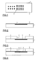
Figure 1 represents a front view of a wafer provided with electrical contact areas; -
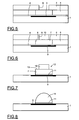
Figures 2 to 8 illustrate different, non-limiting, steps in fabricating electrical bonding pads on a wafer represented in cross section; -
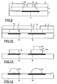
Figure 9 illustrates one step of another embodiment; and -
Figures 9 to 12 illustrate steps of another embodiment. -
Figure 1 represents awafer 1 which has, on itsfront face 2, spaced metallizedelectrical contact areas 3, intended for the electrical connection of this wafer to one or more electronic components by means of electrical bonding pads that can be produced in the following manner, implementing the means and methods currently used in microelectronics. - As
Figure 2 shows, taking awafer 1, a thinintermediate tie layer 4 made of an electrically-conducting material (UBM) is formed on itsfront face 2. - As
Figure 3 shows, afirst layer 5 made of a screen material, for example a photosensitive resin called hereafter photoresist, is formed on theintermediate layer 4 andfirst openings 6 are produced in this first layer over at least some of theelectrical contact areas 3. - As
Figure 4 shows,first blocks 7, made of an electrically conducting (for example, metallic) solder material that conducts electricity, are produced in thefirst openings 6. These blocks can be obtained, for example, by electrolytic growth or deposition. - As
Figure 5 shows, asecond layer 8 made of a screen material, for example a photoresist, is formed on the first layer and on the first blocks produced 7, andsecond openings 9 are produced in this second layer above at least some of thefirst blocks 7 produced. - These
second openings 9 are such that their section is smaller than the section of the upper face of the respectively underlying or correspondingfirst blocks 7 and inscribed in this section. - As
Figure 6 shows,second blocks 10 made of an electrically conducting (for example, metallic) solder material that conducts electricity are produced in thesecond openings 9, these second blocks filling theopenings 9 approximately to their edges and forming an additional supply of material. These blocks can be obtained, for example, by electrolytic growth or deposition. - As
Figure 7 shows, the first andsecond layers intermediate layer 4 is removed or taken off, leavingportions 11 of the intermediate layer under thefirst blocks 7. - What are then obtained are
parts 12 standing out on theconductive areas 3 of thewafer 1, which comprise aportion 11 of theintermediate layer 4, afirst block 7 on this portion and asecond block 10 on this first block, respectively. - According to a variant, the periphery of the
second openings 9 is at a distance from and in the interior of the periphery of the respectively corresponding and underlyingfirst blocks 7, in such a way that thefirst block 7 of each protrudingpart 12 has a peripheralfront shoulder 13 around itssecond block 10. - Then, as shown in
Figure 8 , thewafer 1 is placed in an oven at a temperature such that, by rapid melting, plastic flow and the effect of surface tension, the superposedblocks electrical bonding pads 14. - The material forming the
superposed blocks - According to one exemplary embodiment, the
layers - According to one exemplary embodiment, the
openings solder pads 14 in the form of portions of balls. According to a variant, the side or the diameter of these openings can be between 20 and 150 microns. - According to another exemplary embodiment, the
openings solder pads 14 in the form of bars. In the case where they are to be approximately rectangular, these openings might have a width of between 20 and 150 microns and a length of between 100 and 600 microns. - The profile of the periphery of the
second openings 9, and consequently of thesecond blocks 10, and the profile of the periphery of thefirst openings 6, and consequently of thefirst blocks 7, may ensue in a homothetic manner or be different. - The volumes of material of the
first blocks 7 and the volumes of additional material of thesecond blocks 10 can be adapted to the volumes of material, to the sections and to the heights of theelectrical bonding pads 14 to be obtained. - For example, in the particular case of a final
electrical bonding pad 14 in the form of a bar, the distribution of the material of thefirst block 7 and the distribution of the material of thesecond block 10 can be adapted so that thispad 14 has an end area approximately parallel to the front face of thewafer 1. - According to a variant represented in
Figure 9 , at least two spacedsecond openings second layer 8, on top of an underlyingfirst block 7. Following the steps described above, an additional supply of solder material is provided in at least two places above thisfirst block 7. - According to a variant represented in
Figure 10 ,second openings 9 can be formed in asecond layer 8 only above some of thefirst pads 7a situated above theelectrical contact areas 3a without producing these above someother blocks 7b situated above theelectrical contact areas 3b. - As
Figure 11 shows, following the steps described above, what are obtained are protrudingparts 12a, formed from superposedfirst blocks 7a andsecond blocks 10a, and protruding parts 12b formed fromfirst blocks 7b alone, pads and 12b, shown onfigure 11 . Following the steps described above, the correspondingelectrical bonding pads - As
Figure 11 shows, the dimensions and the volumes of material of thefirst blocks second blocks 9a can, according to a variant of the embodiment, be adapted so that the correspondingelectrical bonding pads - It results from the preceding that, notably, the supply of material due to the production of second blocks superposed on first blocks permits a large degree of adaptability in producing electrical bonding pads, even if the pads have different dimensions on one and the same wafer or are derived from only one first block.
- It also results from the preceding that, notably, electrical contact pads adapted to the passage of relatively high current can be obtained.
Claims (8)
- Method for fabricating electrical bonding pads on the electrical contact areas of a wafer, characterized in that it comprises the following steps:deposition of a first layer made of a screen material;production of first openings in this first layer over at least some of the said electrical contact areas;production of first blocks (7) made of a solder material in the said first openings;deposition of a second layer on the first layer and the first blocks;production of second openings in this second layer, placed above at least some of the first blocks, the section of each second opening being smaller than the section of the upper face of the underlying block;production of second blocks (10) made of a solder material in the said second openings;removal of the material of the first and second layers; andpassage through an oven so as to shape the said blocks into approximately domed electrical bonding pads.
- Method according to Claim 1, characterized in that it comprises a step of producing second openings, the periphery of which is at a distance from and in the interior of the periphery of the corresponding underlying first blocks.
- Method according to one of Claims 1 and 2, characterized in that it comprises a step of producing a single second opening on the corresponding underlying blocks.
- Method according to one of Claims 1 and 2, characterized in that it comprises a step of producing at least two second openings on the corresponding underlying blocks.
- Method according to one of the preceding claims, characterized in that it comprises a step of producing second openings over some of the first blocks and no second opening over other first blocks.
- Method according to Claim 5, characterized in that the pads resulting from the first blocks are approximately circular or in the form of parts of balls, and in that the pads resulting from the superposed first and second blocks are approximately elongate or in the form of bars.
- Method according to one of the preceding claims, characterized in that the quantities of solder material of the said blocks are such that the height of the pads obtained is approximately identical from one pad to another.
- Method according to one of the preceding claims, characterized in that it comprises a preliminary step of depositing an intermediate conducting layer, and in that it comprises a step of removing this layer around the first pads formed before passing through the oven.
Applications Claiming Priority (2)
| Application Number | Priority Date | Filing Date | Title |
|---|---|---|---|
| FR0757254A FR2920634A1 (en) | 2007-08-29 | 2007-08-29 | METHOD FOR MANUFACTURING PLATES FOR THE ELECTRICAL CONNECTION OF A PLATE. |
| PCT/EP2008/058239 WO2009027132A1 (en) | 2007-08-29 | 2008-06-27 | Method for fabricating electrical bonding pads on a wafer |
Publications (2)
| Publication Number | Publication Date |
|---|---|
| EP2181569A1 EP2181569A1 (en) | 2010-05-05 |
| EP2181569B1 true EP2181569B1 (en) | 2011-01-12 |
Family
ID=39264520
Family Applications (1)
| Application Number | Title | Priority Date | Filing Date |
|---|---|---|---|
| EP08774406A Not-in-force EP2181569B1 (en) | 2007-08-29 | 2008-06-27 | Method for fabricating electrical bonding pads on a wafer |
Country Status (7)
| Country | Link |
|---|---|
| US (1) | US8148258B2 (en) |
| EP (1) | EP2181569B1 (en) |
| CN (1) | CN101803479B (en) |
| AT (1) | ATE495652T1 (en) |
| DE (1) | DE602008004552D1 (en) |
| FR (1) | FR2920634A1 (en) |
| WO (1) | WO2009027132A1 (en) |
Family Cites Families (12)
| Publication number | Priority date | Publication date | Assignee | Title |
|---|---|---|---|---|
| EP0723387A1 (en) * | 1995-01-19 | 1996-07-24 | Digital Equipment Corporation | Soldermask gasketing of printed wiring board surface mount pads |
| CN1179412C (en) * | 1995-04-05 | 2004-12-08 | 统一国际有限公司 | Solder structure having elongated portion and widened portion and method of forming same |
| US6042953A (en) * | 1996-03-21 | 2000-03-28 | Matsushita Electric Industrial Co., Ltd. | Substrate on which bumps are formed and method of forming the same |
| US6818545B2 (en) * | 2001-03-05 | 2004-11-16 | Megic Corporation | Low fabrication cost, fine pitch and high reliability solder bump |
| TW483136B (en) * | 2001-03-22 | 2002-04-11 | Apack Technologies Inc | Bump process |
| US6555296B2 (en) * | 2001-04-04 | 2003-04-29 | Siliconware Precision Industries Co., Ltd. | Fine pitch wafer bumping process |
| TW536767B (en) * | 2002-03-01 | 2003-06-11 | Advanced Semiconductor Eng | Solder ball attaching process |
| US6784089B2 (en) * | 2003-01-13 | 2004-08-31 | Aptos Corporation | Flat-top bumping structure and preparation method |
| TWI227557B (en) * | 2003-07-25 | 2005-02-01 | Advanced Semiconductor Eng | Bumping process |
| TWI322491B (en) * | 2003-08-21 | 2010-03-21 | Advanced Semiconductor Eng | Bumping process |
| TWI259572B (en) * | 2004-09-07 | 2006-08-01 | Siliconware Precision Industries Co Ltd | Bump structure of semiconductor package and fabrication method thereof |
| US7459386B2 (en) * | 2004-11-16 | 2008-12-02 | Taiwan Semiconductor Manufacturing Co., Ltd. | Method for forming solder bumps of increased height |
-
2007
- 2007-08-29 FR FR0757254A patent/FR2920634A1/en active Pending
-
2008
- 2008-06-27 WO PCT/EP2008/058239 patent/WO2009027132A1/en not_active Ceased
- 2008-06-27 AT AT08774406T patent/ATE495652T1/en not_active IP Right Cessation
- 2008-06-27 US US12/673,975 patent/US8148258B2/en not_active Expired - Fee Related
- 2008-06-27 EP EP08774406A patent/EP2181569B1/en not_active Not-in-force
- 2008-06-27 CN CN2008801047972A patent/CN101803479B/en not_active Expired - Fee Related
- 2008-06-27 DE DE602008004552T patent/DE602008004552D1/en active Active
Also Published As
| Publication number | Publication date |
|---|---|
| ATE495652T1 (en) | 2011-01-15 |
| EP2181569A1 (en) | 2010-05-05 |
| US20110151657A1 (en) | 2011-06-23 |
| CN101803479B (en) | 2012-04-04 |
| FR2920634A1 (en) | 2009-03-06 |
| CN101803479A (en) | 2010-08-11 |
| DE602008004552D1 (en) | 2011-02-24 |
| WO2009027132A1 (en) | 2009-03-05 |
| US8148258B2 (en) | 2012-04-03 |
Similar Documents
| Publication | Publication Date | Title |
|---|---|---|
| CN106711125B (en) | Semiconductor package and method of manufacturing the same | |
| JP5619276B2 (en) | Microelectronic package having terminals on a dielectric mass | |
| US7767497B2 (en) | Microelectronic package element and method of fabricating thereof | |
| US7482198B2 (en) | Method for producing through-contacts and a semiconductor component with through-contacts | |
| CN109037188A (en) | Semiconductor device package | |
| JP2010087221A5 (en) | ||
| US7456493B2 (en) | Structure for mounting semiconductor part in which bump and land portion are hardly detached from each other and method of manufacturing mounting substrate used therein | |
| US9984989B2 (en) | Semiconductor substrate and semiconductor package structure | |
| CN109727945B (en) | Substrate structure and manufacturing method of semiconductor package element | |
| US9331024B2 (en) | IC wafer having electromagnetic shielding effects and method for making the same | |
| US9474162B2 (en) | Circuit substrate and method of manufacturing same | |
| US8227332B2 (en) | Method for fabricating electrical bonding pads on a wafer | |
| US7525140B2 (en) | Integrated thin film capacitors with adhesion holes for the improvement of adhesion strength | |
| JP2018081979A (en) | Lead frame, electronic component device, and manufacturing method of the same | |
| CN102683298B (en) | Package without carrier board and method for making the same | |
| US8148258B2 (en) | Method for fabricating electrical bonding pads on a wafer | |
| CN109841588A (en) | Semiconductor device packages | |
| CN102224587A (en) | Lead frame, semiconductor device using the same, intermediate product of the semiconductor device, and their manufacturing methods | |
| WO2014127953A1 (en) | Optoelectronic semiconductor component and method for producing same | |
| CN1980530A (en) | Manufacturing method of conductive bump structure on circuit board | |
| JP3211532U (en) | Lead frame preform and lead frame package | |
| US20150123252A1 (en) | Lead frame package and manufacturing method thereof | |
| JP3731805B2 (en) | Circuit board manufacturing method | |
| CN109473416A (en) | Substrate for packaging semiconductor device package and method of manufacturing the same | |
| JP2000349196A (en) | Electroplating method of electronic part and manufacture of the same |
Legal Events
| Date | Code | Title | Description |
|---|---|---|---|
| PUAI | Public reference made under article 153(3) epc to a published international application that has entered the european phase |
Free format text: ORIGINAL CODE: 0009012 |
|
| 17P | Request for examination filed |
Effective date: 20100211 |
|
| AK | Designated contracting states |
Kind code of ref document: A1 Designated state(s): AT BE BG CH CY CZ DE DK EE ES FI FR GB GR HR HU IE IS IT LI LT LU LV MC MT NL NO PL PT RO SE SI SK TR |
|
| AX | Request for extension of the european patent |
Extension state: AL BA MK RS |
|
| GRAP | Despatch of communication of intention to grant a patent |
Free format text: ORIGINAL CODE: EPIDOSNIGR1 |
|
| DAX | Request for extension of the european patent (deleted) | ||
| GRAS | Grant fee paid |
Free format text: ORIGINAL CODE: EPIDOSNIGR3 |
|
| GRAA | (expected) grant |
Free format text: ORIGINAL CODE: 0009210 |
|
| AK | Designated contracting states |
Kind code of ref document: B1 Designated state(s): AT BE BG CH CY CZ DE DK EE ES FI FR GB GR HR HU IE IS IT LI LT LU LV MC MT NL NO PL PT RO SE SI SK TR |
|
| REG | Reference to a national code |
Ref country code: GB Ref legal event code: FG4D |
|
| REG | Reference to a national code |
Ref country code: CH Ref legal event code: EP |
|
| REG | Reference to a national code |
Ref country code: IE Ref legal event code: FG4D |
|
| REF | Corresponds to: |
Ref document number: 602008004552 Country of ref document: DE Date of ref document: 20110224 Kind code of ref document: P |
|
| REG | Reference to a national code |
Ref country code: DE Ref legal event code: R096 Ref document number: 602008004552 Country of ref document: DE Effective date: 20110224 |
|
| REG | Reference to a national code |
Ref country code: NL Ref legal event code: VDEP Effective date: 20110112 |
|
| LTIE | Lt: invalidation of european patent or patent extension |
Effective date: 20110112 |
|
| PG25 | Lapsed in a contracting state [announced via postgrant information from national office to epo] |
Ref country code: HR Free format text: LAPSE BECAUSE OF FAILURE TO SUBMIT A TRANSLATION OF THE DESCRIPTION OR TO PAY THE FEE WITHIN THE PRESCRIBED TIME-LIMIT Effective date: 20110112 Ref country code: ES Free format text: LAPSE BECAUSE OF FAILURE TO SUBMIT A TRANSLATION OF THE DESCRIPTION OR TO PAY THE FEE WITHIN THE PRESCRIBED TIME-LIMIT Effective date: 20110423 Ref country code: PT Free format text: LAPSE BECAUSE OF FAILURE TO SUBMIT A TRANSLATION OF THE DESCRIPTION OR TO PAY THE FEE WITHIN THE PRESCRIBED TIME-LIMIT Effective date: 20110512 Ref country code: GR Free format text: LAPSE BECAUSE OF FAILURE TO SUBMIT A TRANSLATION OF THE DESCRIPTION OR TO PAY THE FEE WITHIN THE PRESCRIBED TIME-LIMIT Effective date: 20110413 Ref country code: LT Free format text: LAPSE BECAUSE OF FAILURE TO SUBMIT A TRANSLATION OF THE DESCRIPTION OR TO PAY THE FEE WITHIN THE PRESCRIBED TIME-LIMIT Effective date: 20110112 Ref country code: IS Free format text: LAPSE BECAUSE OF FAILURE TO SUBMIT A TRANSLATION OF THE DESCRIPTION OR TO PAY THE FEE WITHIN THE PRESCRIBED TIME-LIMIT Effective date: 20110512 Ref country code: LV Free format text: LAPSE BECAUSE OF FAILURE TO SUBMIT A TRANSLATION OF THE DESCRIPTION OR TO PAY THE FEE WITHIN THE PRESCRIBED TIME-LIMIT Effective date: 20110112 Ref country code: NO Free format text: LAPSE BECAUSE OF FAILURE TO SUBMIT A TRANSLATION OF THE DESCRIPTION OR TO PAY THE FEE WITHIN THE PRESCRIBED TIME-LIMIT Effective date: 20110412 Ref country code: SE Free format text: LAPSE BECAUSE OF FAILURE TO SUBMIT A TRANSLATION OF THE DESCRIPTION OR TO PAY THE FEE WITHIN THE PRESCRIBED TIME-LIMIT Effective date: 20110112 |
|
| PG25 | Lapsed in a contracting state [announced via postgrant information from national office to epo] |
Ref country code: AT Free format text: LAPSE BECAUSE OF FAILURE TO SUBMIT A TRANSLATION OF THE DESCRIPTION OR TO PAY THE FEE WITHIN THE PRESCRIBED TIME-LIMIT Effective date: 20110112 Ref country code: NL Free format text: LAPSE BECAUSE OF FAILURE TO SUBMIT A TRANSLATION OF THE DESCRIPTION OR TO PAY THE FEE WITHIN THE PRESCRIBED TIME-LIMIT Effective date: 20110112 Ref country code: CY Free format text: LAPSE BECAUSE OF FAILURE TO SUBMIT A TRANSLATION OF THE DESCRIPTION OR TO PAY THE FEE WITHIN THE PRESCRIBED TIME-LIMIT Effective date: 20110112 Ref country code: PL Free format text: LAPSE BECAUSE OF FAILURE TO SUBMIT A TRANSLATION OF THE DESCRIPTION OR TO PAY THE FEE WITHIN THE PRESCRIBED TIME-LIMIT Effective date: 20110112 Ref country code: BG Free format text: LAPSE BECAUSE OF FAILURE TO SUBMIT A TRANSLATION OF THE DESCRIPTION OR TO PAY THE FEE WITHIN THE PRESCRIBED TIME-LIMIT Effective date: 20110412 Ref country code: SI Free format text: LAPSE BECAUSE OF FAILURE TO SUBMIT A TRANSLATION OF THE DESCRIPTION OR TO PAY THE FEE WITHIN THE PRESCRIBED TIME-LIMIT Effective date: 20110112 Ref country code: BE Free format text: LAPSE BECAUSE OF FAILURE TO SUBMIT A TRANSLATION OF THE DESCRIPTION OR TO PAY THE FEE WITHIN THE PRESCRIBED TIME-LIMIT Effective date: 20110112 Ref country code: FI Free format text: LAPSE BECAUSE OF FAILURE TO SUBMIT A TRANSLATION OF THE DESCRIPTION OR TO PAY THE FEE WITHIN THE PRESCRIBED TIME-LIMIT Effective date: 20110112 |
|
| PG25 | Lapsed in a contracting state [announced via postgrant information from national office to epo] |
Ref country code: EE Free format text: LAPSE BECAUSE OF FAILURE TO SUBMIT A TRANSLATION OF THE DESCRIPTION OR TO PAY THE FEE WITHIN THE PRESCRIBED TIME-LIMIT Effective date: 20110112 Ref country code: DK Free format text: LAPSE BECAUSE OF FAILURE TO SUBMIT A TRANSLATION OF THE DESCRIPTION OR TO PAY THE FEE WITHIN THE PRESCRIBED TIME-LIMIT Effective date: 20110112 |
|
| PLBE | No opposition filed within time limit |
Free format text: ORIGINAL CODE: 0009261 |
|
| STAA | Information on the status of an ep patent application or granted ep patent |
Free format text: STATUS: NO OPPOSITION FILED WITHIN TIME LIMIT |
|
| PG25 | Lapsed in a contracting state [announced via postgrant information from national office to epo] |
Ref country code: CZ Free format text: LAPSE BECAUSE OF FAILURE TO SUBMIT A TRANSLATION OF THE DESCRIPTION OR TO PAY THE FEE WITHIN THE PRESCRIBED TIME-LIMIT Effective date: 20110112 Ref country code: SK Free format text: LAPSE BECAUSE OF FAILURE TO SUBMIT A TRANSLATION OF THE DESCRIPTION OR TO PAY THE FEE WITHIN THE PRESCRIBED TIME-LIMIT Effective date: 20110112 Ref country code: RO Free format text: LAPSE BECAUSE OF FAILURE TO SUBMIT A TRANSLATION OF THE DESCRIPTION OR TO PAY THE FEE WITHIN THE PRESCRIBED TIME-LIMIT Effective date: 20110112 |
|
| 26N | No opposition filed |
Effective date: 20111013 |
|
| PG25 | Lapsed in a contracting state [announced via postgrant information from national office to epo] |
Ref country code: MT Free format text: LAPSE BECAUSE OF FAILURE TO SUBMIT A TRANSLATION OF THE DESCRIPTION OR TO PAY THE FEE WITHIN THE PRESCRIBED TIME-LIMIT Effective date: 20110112 |
|
| REG | Reference to a national code |
Ref country code: DE Ref legal event code: R097 Ref document number: 602008004552 Country of ref document: DE Effective date: 20111013 |
|
| REG | Reference to a national code |
Ref country code: IE Ref legal event code: MM4A |
|
| PG25 | Lapsed in a contracting state [announced via postgrant information from national office to epo] |
Ref country code: IE Free format text: LAPSE BECAUSE OF NON-PAYMENT OF DUE FEES Effective date: 20110627 |
|
| PGFP | Annual fee paid to national office [announced via postgrant information from national office to epo] |
Ref country code: GB Payment date: 20120525 Year of fee payment: 5 |
|
| PGFP | Annual fee paid to national office [announced via postgrant information from national office to epo] |
Ref country code: IT Payment date: 20120519 Year of fee payment: 5 |
|
| REG | Reference to a national code |
Ref country code: CH Ref legal event code: PL |
|
| REG | Reference to a national code |
Ref country code: CH Ref legal event code: PL |
|
| PG25 | Lapsed in a contracting state [announced via postgrant information from national office to epo] |
Ref country code: CH Free format text: LAPSE BECAUSE OF NON-PAYMENT OF DUE FEES Effective date: 20120630 Ref country code: LI Free format text: LAPSE BECAUSE OF NON-PAYMENT OF DUE FEES Effective date: 20120630 Ref country code: MC Free format text: LAPSE BECAUSE OF NON-PAYMENT OF DUE FEES Effective date: 20110630 |
|
| PG25 | Lapsed in a contracting state [announced via postgrant information from national office to epo] |
Ref country code: LU Free format text: LAPSE BECAUSE OF NON-PAYMENT OF DUE FEES Effective date: 20110627 |
|
| PGFP | Annual fee paid to national office [announced via postgrant information from national office to epo] |
Ref country code: DE Payment date: 20130523 Year of fee payment: 6 |
|
| PG25 | Lapsed in a contracting state [announced via postgrant information from national office to epo] |
Ref country code: TR Free format text: LAPSE BECAUSE OF FAILURE TO SUBMIT A TRANSLATION OF THE DESCRIPTION OR TO PAY THE FEE WITHIN THE PRESCRIBED TIME-LIMIT Effective date: 20110112 |
|
| PG25 | Lapsed in a contracting state [announced via postgrant information from national office to epo] |
Ref country code: HU Free format text: LAPSE BECAUSE OF FAILURE TO SUBMIT A TRANSLATION OF THE DESCRIPTION OR TO PAY THE FEE WITHIN THE PRESCRIBED TIME-LIMIT Effective date: 20110112 |
|
| PGFP | Annual fee paid to national office [announced via postgrant information from national office to epo] |
Ref country code: FR Payment date: 20130724 Year of fee payment: 6 |
|
| GBPC | Gb: european patent ceased through non-payment of renewal fee |
Effective date: 20130627 |
|
| PG25 | Lapsed in a contracting state [announced via postgrant information from national office to epo] |
Ref country code: GB Free format text: LAPSE BECAUSE OF NON-PAYMENT OF DUE FEES Effective date: 20130627 |
|
| PG25 | Lapsed in a contracting state [announced via postgrant information from national office to epo] |
Ref country code: IT Free format text: LAPSE BECAUSE OF NON-PAYMENT OF DUE FEES Effective date: 20130627 |
|
| REG | Reference to a national code |
Ref country code: DE Ref legal event code: R119 Ref document number: 602008004552 Country of ref document: DE |
|
| REG | Reference to a national code |
Ref country code: FR Ref legal event code: ST Effective date: 20150227 |
|
| REG | Reference to a national code |
Ref country code: DE Ref legal event code: R119 Ref document number: 602008004552 Country of ref document: DE Effective date: 20150101 |
|
| PG25 | Lapsed in a contracting state [announced via postgrant information from national office to epo] |
Ref country code: DE Free format text: LAPSE BECAUSE OF NON-PAYMENT OF DUE FEES Effective date: 20150101 |
|
| PG25 | Lapsed in a contracting state [announced via postgrant information from national office to epo] |
Ref country code: FR Free format text: LAPSE BECAUSE OF NON-PAYMENT OF DUE FEES Effective date: 20140630 |