EP2180263A2 - Refrigeration cycle apparatus as well as air conditioner and water heater having the same - Google Patents
Refrigeration cycle apparatus as well as air conditioner and water heater having the same Download PDFInfo
- Publication number
- EP2180263A2 EP2180263A2 EP09166564A EP09166564A EP2180263A2 EP 2180263 A2 EP2180263 A2 EP 2180263A2 EP 09166564 A EP09166564 A EP 09166564A EP 09166564 A EP09166564 A EP 09166564A EP 2180263 A2 EP2180263 A2 EP 2180263A2
- Authority
- EP
- European Patent Office
- Prior art keywords
- side unit
- voltage
- microcomputer
- circuit
- cables
- Prior art date
- Legal status (The legal status is an assumption and is not a legal conclusion. Google has not performed a legal analysis and makes no representation as to the accuracy of the status listed.)
- Granted
Links
Images



Classifications
-
- F—MECHANICAL ENGINEERING; LIGHTING; HEATING; WEAPONS; BLASTING
- F24—HEATING; RANGES; VENTILATING
- F24F—AIR-CONDITIONING; AIR-HUMIDIFICATION; VENTILATION; USE OF AIR CURRENTS FOR SCREENING
- F24F1/00—Room units for air-conditioning, e.g. separate or self-contained units or units receiving primary air from a central station
- F24F1/06—Separate outdoor units, e.g. outdoor unit to be linked to a separate room comprising a compressor and a heat exchanger
- F24F1/20—Electric components for separate outdoor units
- F24F1/22—Arrangement or mounting thereof
-
- F—MECHANICAL ENGINEERING; LIGHTING; HEATING; WEAPONS; BLASTING
- F25—REFRIGERATION OR COOLING; COMBINED HEATING AND REFRIGERATION SYSTEMS; HEAT PUMP SYSTEMS; MANUFACTURE OR STORAGE OF ICE; LIQUEFACTION SOLIDIFICATION OF GASES
- F25B—REFRIGERATION MACHINES, PLANTS OR SYSTEMS; COMBINED HEATING AND REFRIGERATION SYSTEMS; HEAT PUMP SYSTEMS
- F25B49/00—Arrangement or mounting of control or safety devices
- F25B49/005—Arrangement or mounting of control or safety devices of safety devices
-
- F—MECHANICAL ENGINEERING; LIGHTING; HEATING; WEAPONS; BLASTING
- F24—HEATING; RANGES; VENTILATING
- F24F—AIR-CONDITIONING; AIR-HUMIDIFICATION; VENTILATION; USE OF AIR CURRENTS FOR SCREENING
- F24F11/00—Control or safety arrangements
- F24F11/50—Control or safety arrangements characterised by user interfaces or communication
- F24F11/52—Indication arrangements, e.g. displays
-
- F—MECHANICAL ENGINEERING; LIGHTING; HEATING; WEAPONS; BLASTING
- F24—HEATING; RANGES; VENTILATING
- F24F—AIR-CONDITIONING; AIR-HUMIDIFICATION; VENTILATION; USE OF AIR CURRENTS FOR SCREENING
- F24F2221/00—Details or features not otherwise provided for
- F24F2221/32—Details or features not otherwise provided for preventing human errors during the installation, use or maintenance, e.g. goofy proof
-
- F—MECHANICAL ENGINEERING; LIGHTING; HEATING; WEAPONS; BLASTING
- F25—REFRIGERATION OR COOLING; COMBINED HEATING AND REFRIGERATION SYSTEMS; HEAT PUMP SYSTEMS; MANUFACTURE OR STORAGE OF ICE; LIQUEFACTION SOLIDIFICATION OF GASES
- F25B—REFRIGERATION MACHINES, PLANTS OR SYSTEMS; COMBINED HEATING AND REFRIGERATION SYSTEMS; HEAT PUMP SYSTEMS
- F25B2700/00—Sensing or detecting of parameters; Sensors therefor
- F25B2700/15—Power, e.g. by voltage or current
Definitions
- the present invention relates to a refrigeration cycle apparatus as well as an air conditioner and a water heater having the same, and more particularly, to protection of an internal circuit against faulty wiring in two apparatuses connected by a power supply line and communication line.
- an excess voltage detector is disposed to a communication circuit terminal part, whose output, a relay contact, is connected in series to a communication circuit, and when an excess voltage is applied to the communication circuit, the circuit is electrically disconnected from the communication circuit terminal instantly.
- a conventional refrigeration cycle apparatus is mounted which has a protective function for protecting a substrate and electronic parts and the like constituting an internal circuit when power supply cables and signal cables are faultily wired (refer to, for example, Japanese Unexamined Patent Application Publication No. 7-217972 ).
- Patent Document 1 Japanese Unexamined Patent Application Publication No. 7-217972
- the object of the present invention which was made to solve the above problems, is to provide a refrigeration cycle apparatus capable of protecting faulty wiring while saving or not using an additional substrate space necessary to protect them and reducing a cost or without an additional cost.
- a refrigeration cycle apparatus including a user side unit and a heat source side unit connected to each other by at least three cables through the connection ends thereof, the user side unit and the heat source side unit have communication circuits, respectively;
- One unit of the user side unit and the heat source side unit receives an alternating voltage from an alternating current source, supplies electrical power to the other unit of the user side unit and the heat source side unit through the connection ends using two cables of the three cables as alternating current cables, a current loop is formed using a remaining cable and one of the alternating current cables as communication cables constituting the communication circuit a communication is executed through the connection ends, the other unit has a zero cross circuit for detecting a zero cross point of the alternating voltage received from the one unit and judges whether the three cables are faultily wired from an output from the zero cross circuit, and when the three cables are faultily wired, the other unit shuts down the communication circuit.
- the refrigeration cycle apparatus detects the faulty wiring by using a zero cross circuit originally used for a different object, it has an advantage in that no space is additionally required to detect the faulty wiring and a cost is not increased.
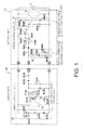
- Fig. 1 is a schematic view of a configuration circuit of a refrigeration cycle apparatus according to Embodiment 1
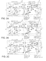
- Fig. 2A - 2C are diagrams showing combinations of faultily wired cables of a heat source side unit of an outdoor unit and a user side unit of an indoor unit
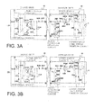
- Fig. 3A - 3B are diagrams showing combinations of faultily wired cables of the heat source side unit of the outdoor unit and the user side unit of the indoor unit.
- S1, S2, and S3 are terminal numbers of terminal boards of the heat source side unit 51 of the outdoor unit and the user side unit 52 of the indoor unit, and the cables are normally wired when they are wired so that the terminal numbers of the indoor unit agree with those of the outdoor unit.
- An external alternating current source 1 of the heat source side unit 51 is connected to both the ends of a power supply circuit 2 disposed in the heat source side unit 51.
- a diode D602, a resistor R607, and a zener diode ZD602, which are connected in series, are connected in parallel to both the ends of the power supply circuit 2, a connection point, at which the power supply circuit 2 is connected to the diode D602, is connected to a terminal S1, and a connection point, at which the power supply circuit 2 is connected to the zener diode ZD602, is connected to a terminal S2.
- a capacitor C603 is connected in parallel to both the ends of the zener diode ZD602, and a communication power supply creation circuit 3 is composed of the diode D602, resistor R607, zener diode ZD602, and capacitor C603.
- a transmission photocoupler PC602, a reception photocoupler PC601, a diode D601, and a resistor R601 are connected in series in this order from the connection point of the resistor R607 and the zener diode ZD602, and the other end of the resistor R601 is connected to a terminal S3 of a terminal board. Further, a resistor R602 and a capacitor C602 are connected in parallel to both the ends of the reception photocoupler PC601, respectively. Then, a resistor R605, a diode D605, and a resistor R603, which are connected in series, are connected between the terminal S3 and the terminal S2.
- a photocoupler PC603 is connected in parallel to both the ends of the resistor R603, and a faulty connection detecting circuit 4 is composed of the resistor R605, diode D605, resistor R603, photocoupler PC603, and other parts which are not shown in Fig. 1 .
- a resistor R132, a diode D132, a reception photocoupler IC132, and a transmission photocoupler IC131 are connected in series in this order from the terminal S3 and finally connected to the terminal S2 to thereby constitute a communication circuit. Further, a diode D131 and a capacitor C134 are connected in parallel to both the ends of the reception photocoupler IC132 and the transmission photocoupler IC131 connected in series. Then, a resistor R133 and a capacitor C133 are connected in parallel to both the ends of the reception photocoupler IC132, respectively.
- a power supply circuit 11 is connected to the terminals S1 and S2. Further, a diode D122, a resistor R121, and a diode D121, which are connected in series, are connected in parallel to both the ends of the power supply circuit 11. Then, a photocoupler IC121 is connected to both the ends of the diode D122, and a zero cross circuit 12 is composed of the diode D122, resistor R121, diode D121, photocoupler IC121, and parts composed of other parts which are not shown in Fig. 1 .
- the alternating current source 1 supplies an alternating voltage to the power supply circuit 2 which creates a direct voltage to be supplied to internal IC parts and the like. Further, the alternating voltage supplied by the alternating current source 1 is half-wave rectified by the diode D602 and the half-wave rectified current is restricted by the resistor R607. Then, a constant voltage is created by the zener diode ZD602 and further smoothed by the capacitor C603, thereby a communication power supply of about 25V is created.
- a current loop is formed by the circuit configuration in the heat source side unit 51 and the user side unit 52 and the paths in which the terminals S3, S3 and the terminals S2, S2 are connected to each other. Further, the resistor R601 in the heat source side unit 51 and the resistor R132 in the user side unit 52 restrict a current flowing in the current loop to thereby suppress an excess current. Further, the diode D601 in the heat source side unit 51 and the diode D132 in the user side unit 52 restrict the direction of the current of the current loop.
- the transmission photocoupler PC602 in the heat source side unit 51 and the transmission photocoupler IC131 in the user side unit 52 generates an ON and OFF state of the current flowing in the current loop, and the heat source side unit 51 and the user side unit 52 communicate with each other when the reception photocoupler PC601 in the heat source side unit 51 and the reception photocoupler IC132 in the user side unit 52 detect the ON/OFF of the current.
- the faulty connection detecting circuit 4 detects faulty connection to the alternating current source and to the ground in the heat source side unit 51.
- the zero cross circuit 12 detects a zero cross point of an alternating voltage that is input between the terminals S1 and S2 of the user side unit 52 from the heat source side unit 51. Then, the alternating voltage is supplied from the terminals S1 and S2 to the power supply circuit 11 to thereby create a direct voltage to be supplied to the internal IC parts and the like.
- Figs. 2A - 2C and 3A - 3B an operation when the heat source side unit 51 and the user side unit 52 are faultily connected will be explained referring to Figs. 2A - 2C and 3A - 3B .
- an alternating voltage may be applied to a low voltage circuit portion, i.e., a communication circuit of the user side unit 52 due to faulty wiring among the terminals S1, S2, and S3 of the indoor unit and the outdoor unit (refer to Fig. 2B and Fig. 3A ).
- a high voltage withstanding photocoupler is used as the transmission photocoupler IC131 to protect the diode D131 and the diode D132 so that a current does not flow thereto.
- the transmission photocoupler IC131 As one of method of the prevention, it is possible to prevent the transmission photocoupler IC131 from being turned ON by detecting that faulty wiring among the terminals S1, S2, and S3 of the indoor unit and the outdoor unit by also using the zero cross circuit 12 used for a different object such as a cutoff of the alternating voltage input, a long time timer, and the like.
- the zero cross circuit 12 used for a different object such as a cutoff of the alternating voltage input, a long time timer, and the like.
- no alternating voltage is applied to the zero cross circuit 12 and its zero cross detection output is not input to a microcomputer (not shown). Since it can be judged by the above operation that it is faulty wiring, the communication circuit can be protected by preventing the transmission photocoupler IC131 from being turned ON.
- the communication circuit can be protected by detecting faulty wiring among the terminals S1, S2, and S3 of the indoor unit and the outdoor unit by diverting the zero cross circuit 12 for a different object and preventing the transmission photocoupler IC131 from being turned ON. Further, since it is not necessary to add new parts only for the purpose of protecting the faulty wiring, faulty wiring can be protected without increasing a space at free of cost.
- the heat source side unit 51 of the outdoor unit receives an alternating voltage from the alternating current source 1, the communication power supply is created by the communication power supply creation circuit 3 disposed therein, and the user side unit 52 of the indoor unit includes the zero cross circuit 12.
- the user side unit 52 of the indoor unit may receive an alternating voltage from the alternating current source 1, the communication power supply creation circuit 3 may be disposed therein, and the heat source side unit 51 of the outdoor unit may include the zero cross circuit 12.
- Fig. 4 is a schematic view of a power supply circuit 11 of a user side unit 52 of an indoor unit of a refrigeration cycle apparatus according to Embodiment 2, showing only minimum parts. A configuration and an operation which are different from those of Embodiment 1 described above will be mainly explained below. In Embodiment 2, a method of protecting faulty wiring among terminals S1, S2, and S3 of an indoor unit and an outdoor unit when no zero cross circuit 12 is installed will be explained.
- a circuit configuration of a power supply circuit 11 will be explained while referring to Fig. 4 .
- the terminals S1 and S2 of the user side unit 52 are connected to an input side of a diode bridge DB1.
- a smoothing capacitor C111 is connected in parallel to an output end of the diode bridge DB1.
- a primary side of a transformer T111 and a switching element IC111 which are connected in series, are connected in parallel to both the ends of the smoothing capacitor C111.
- a secondary side of the transformer T111 i.e., one end of the output end of the transformer T111 is connected to an input terminal of a three-terminal regulator IC112 through a diode P113.
- a smoothing capacitor C113 is connected to the input terminal of the three-terminal regulator IC112 and to the other end of the output ends of the transformer T111, and the other end of the output ends of the transformer T111 is connected to a COM terminal of the three-terminal regulator IC112.
- a load resistor R1 is connected in parallel to both the ends of the smoothing capacitor C113.
- an output terminal of the three-terminal regulator IC112 is connected to one end of a smoothing capacitor C116, and the other end thereof is connected to the COM terminal of the three-terminal regulator IC112 and grounded. Further, the output terminal of the three-terminal regulator IC112 is connected to a microcomputer 21 and a reset IC 22, and an output terminal of the reset IC 22 is connected to the microcomputer 21.
- a voltage transmitted from the primary side through the transformer T111 is half-wave rectified by a diode D113.
- the half-wave rectified voltage is smoothed by the smoothing capacitor C113 and creates a VDD12V power supply at both the ends of the smoothing capacitor C113.
- the voltage of the VDD12V power supply is dropped by the three-terminal regulator IC112 to create a VDD5V power supply, which is a microcomputer drive power supply.
- the VDD5V power supply is smoothed by the smoothing capacitor C116.
- a reset IC 22 monitors the microcomputer drive power supply VDD5V, and when its voltage is lower than a predetermined voltage, the reset IC 22 outputs a reset signal to the microcomputer 21 so that it is not driven.
- Figs. 1 to 3B an operation when the heat source side unit 51 and the user side unit 52 are faultily wired will be explained while referring to Figs. 1 to 3B .
- an alternating voltage is not directly input between terminals S1 and S2 of the user side unit 52.
- a communication power supply is input to an alternating voltage terminal at the user side unit 52 side in Fig. 2B and Fig. 3B , and is input thereto through a faulty connection detecting circuit in Fig. 2C and Fig. 3B .
- the switching element IC111 is intermittently switched in such a manner that the turned-ON state of the switching element IC111 does not continue and a switching operation is resumed when the voltage between both the ends of the smoothing capacitor C111 is set to a predetermined voltage necessary to start the switching element IC111 again.
- the voltage on the secondary side is not stabilized because it is periodically charged and discharged repeatedly.
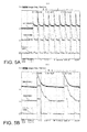
- Ch1 is set to VDD12V
- Ch2 is set to VDD5V
- Ch3 is set to an output of the reset IC 22 (Hi is in a reset release state).
- Vdd12V does not sufficiently rise in the state that the power supply capability is poor at the time of faulty wiring. Further, VDD5D created based thereon comes not to sufficiently rise as well, so that it is possible to make reset not to be released by suppressing VDD5V lower than a voltage for releasing the reset IC22 (hereinafter, a reset release voltage).
- a difference in the input voltage and output voltage of a three-terminal regulator is about 2 V.
- the reset IC 22 when the reset release voltage of the reset IC 22 is set to 4 V, the reset IC 22 can be prevented from executing a reset operation by connecting the load resistor R1 for setting the MAX value of VDD12V to 6 V or less when the power supply capability is very low in the case of the faulty wiring.
- a voltage which is divided by the faulty connection detecting circuit 4 and the impedance of the power supply circuit 11 in the user side unit 52, is applied to the terminals S1 and S2 of the user side unit 52.
- a resistor R605 has a large resistance value of 100 k ⁇ , the voltage applied to the terminals S1 and S2 of the user side unit 52 is suppressed to a low level, and a current is also greatly reduced in addition. Accordingly, since a power supply capability to the user side unit 52 is very low like the case of the faultily wired states of Fig. 2B and Fig. 3B , rising of VDD12V and VDD5V due to the supply of the power is suppressed by connecting the load resistor R1 so that it is possible to make the reset release by the reset IC22 not to be executed.
- the load resistor R1 must be set to a value that causes no problem when the power supply rises at the time of normal wiring as shown in Fig. 1 , however, the value can be set without problem because the power supply capability has an apparent difference in the normally wired states shown in Fig. 1 and the faultily wired states shown in Fig 2B and Fig. 2C and Fig 3A and Fig. 3B . Further, in the faultily wired state of Fig. 2A , no alternating voltage as a high voltage is applied to the communication circuit, no destruction therein.
- the heat source side unit 51 in the outdoor unit receives an alternating voltage from an alternating power supply 1 and supplies it to the user side unit 52 in the indoor unit, and the user side unit 52 in the indoor unit has the power supply circuit 11 for enabling the protection of the faultily wiring described above.
- the user side unit 52 in the indoor unit may receive an alternating voltage from the alternating power supply 1 and supply it to the heat source side unit 51 in the outdoor unit, and the power supply circuit 2 of the heat source side unit 51 in the outdoor unit can protect the faulty wiring mentioned above.
- Embodiment 3 An configuration and an operation which are different from those of Embodiment 2 will be mainly explained in the following explanation of Embodiment 3.
- the load resistor R1 is disposed to the secondary side of the transformer T111 in Embodiment 2
- a load resistor R2 is connected in parallel to both the ends of a smoothing capacitor C111 on its primary side in Embodiment 3 as shown in Fig. 4 .
- a switching element IC111 can be made to be a switching OFF state by providing an appropriate resistor as the load resistor R2 and sufficiently suppressing rising of a voltage between both the ends of the smoothing capacitor C111.
- the transmission photocoupler IC131 is not turned ON and the communication circuit can be protected. Further, it is also possible to protect the faulty wiring by combining Embodiments 2 and 3.
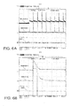
- Fig. 6A - 6B are voltage waveform diagrams of a secondary side when a delay is provided until a reset is released at the time of faulty wiring in a refrigeration cycle apparatus according to Embodiment 4.
- a configuration and an operation which are different from those of Embodiments 2 and 3 will be mainly explained in the following explanation of Embodiment 4.
- the load resistor R1 is provided in Embodiment 2 and the load resistor R2 is provided in Embodiment 3 so that a reset is not released by the reset IC22.
- a delay is provided until the reset IC 22 releases a reset after VDD5V reaches a reset release voltage. With this operation, in a minute time during which VDD5V becomes equal to or higher than the reset release voltage, it is possible to prevent the reset IC 22 from releasing the reset.
- VDD5V is set equal to or higher than the reset release voltage as shown in Fig. 6A - 6B , it can be confirmed that the reset is not released by the provision of the delay.
- the delay of the reset release time must be suppressed within a time by which a control is not interfered at the time of normal wiring.
- a transmission photocoupler IC131 is not turned ON and a communication circuit can be protected. Further, provision of the delay can prevent the reset IC22 from releasing the reset, the load resistor R1 or R2 can be set to a high resistance value, and power consumed by these load resistors can be suppressed at the time of normal wiring.
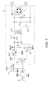
- Fig. 7 is a power supply circuit diagram when a load resistor is caused to consume no power while a refrigeration cycle apparatus according to Embodiment 5 is operated in the case of normal wiring.
- a configuration and an operation which are different from those of Embodiments 2 to 4 described above will be mainly explained in the following explanation of Embodiment 5.
- an output terminal of a 3-terminal regulator IC112 is connected to an emitter of a PNP transistor Q1. Further, a collector of the PNP transistor Q1 is connected to a base of an NPN transistor Q2. Further, the other end of a load resistor R1 having one end connected to an input terminal of the 3-terminal regulator IC112 is connected to a collector of the NPN transistor Q2. Then, an emitter of the NPN transistor Q2 is connected to one end of a smoothing capacitor C113 as well as to the ground. Further, an output terminal of the reset IC 22 and a microcomputer 21 are connected to a base of the PNP transistor Q1.
- Embodiments 2 to 4 it is also possible to protect the faulty wiring by combining Embodiments 2 to 4 and Embodiment 5.
- Fig. 8 is a view showing a communication start delay time provided by a program of a microcomputer 21 in a refrigeration cycle apparatus according to Embodiment 6. A configuration and an operation which are different from those of Embodiment 2 will be mainly explained in the following explanation of Embodiment 6.
- Embodiment 2 to prevent a reset from being released by the reset IC 22, a rising of VDD5V is suppressed by disposing the load resistor R1 so that the reset is not released by the reset IC 22.
- the rising of VDD5V itself is not suppressed by hardware such as electronic parts and the like, but a predetermined delay time, i.e., a communication start delay time t is provided before a communication star by the program of the microcomputer 21 after a reset is released by the reset IC 22 in response to the rising of the VDD5V. Since a power supply capability is low in the faultily wired states shown in Fig. 2B and Fig. 2C and Fig. 3A and Fig. 3B by providing the communication start delay time t, the VDD5V drops during the communication start delay time t so that the device becomes a reset state again.
- a transmission photocoupler IC131 does not turn ON and a communication circuit can be protected. Further, since faulty wiring can be protected by software which is a program of the microcomputer 21 in place of hardware such as electronic parts and the like, additional space is not necessary and cost is not increased.
- Embodiments 2 to 5 It is also possible to protect the faulty wiring by combining Embodiments 2 to 5 and Embodiment 6.
- Fig. 9 is a schematic view of a configuration circuit of a refrigeration cycle apparatus according to Embodiment 7. A configuration and an operation which are different from those of Embodiment 2 described above will be mainly explained in the following explanation of Embodiment 7.
- a low input voltage detection means 31 which detects a rectified and smoothed voltage, is connected in parallel to a capacitor C111, and wiring is executed so that a switching element IC111 can be turned on and off in response to a voltage detected thereby.
- An existing switching element may have a low input voltage detection function and becomes switching OFF state when detecting a low voltage, it is also possible to use it.
- the function can be used without adding a sensing resistor or an additional part, space saving and cost reduction can be realized.
- a similar effect can be also obtained by using a switching element having a switching start activation voltage higher than a low voltage input in the faultily wired states in Fig. 2B and Fig. 2C and Fig. 3A and Fig. 3B .
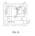
- Fig. 10 shows an example of a configuration view when a refrigeration cycle apparatus according to any of Embodiments 1 to 7 is mounted on an air conditioner.
- a flow path of a refrigerant circulating in the refrigeration cycle of the air conditioner according to Embodiment 8 passes firstly from a compressor 61 of an outdoor unit 101 through a 4-way valve 62, a first heat exchanger 63, and an expansion valve 64 and flows out to the outside of the outdoor unit 101.
- the refrigerant flowed out to the outside of the outdoor unit 101 flows out to the outside of an indoor unit 102 through a second heat exchanger 65 in the indoor unit 102.
- the refrigerant which is flowed out to the outside of the indoor unit 102 returns again to the compressor 61 through the 4-way valve 62 in the outdoor unit 101.
- Heat exchange with an external air is performed in the first heat exchanger 63, and heat exchange with an indoor air is performed in the second heat exchanger 65.
- a heat source side unit 51 is disposed in the outdoor unit 101, and an alternating voltage is supplied from an external alternating current source 1. Further, a user side unit 52 is installed in the indoor unit 102 and electrically connected to the heat source side unit 51 in the outdoor unit 101 according to the configurations explained in Embodiments 1 to 7.
- the air conditioner can be obtained which is provided with the refrigeration cycle apparatus in which faulty wiring is protected as explained in Embodiments 1 to 7.
- the configuration of the air conditioner shown in Fig. 10 is only an example, and the refrigeration cycle apparatuses according to Embodiments 1 to 7 having a different configuration may be mounted thereon.
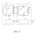
- Fig. 11 shows an example of an configuration view when the refrigeration cycle apparatus according to any of Embodiments 1 to 7 is mounted on a water heater.
- a refrigeration cycle is composed of a compressor 61, a radiator 67, an expansion valve 64 and an evaporator 66.
- a refrigerant flow path circulating in the refrigeration cycle passes from the compressor 61 through the radiator 67, the expansion valve 64, and the evaporator 66, and returns to the compressor 61 again.
- a water circulation cycle is composed of a pump 69, a radiator 67, and a tank 68.
- a water flow path circulating in the water circulation cycle passes from the pump 69 through the radiator 67 and the tank 68 and returns to the pump 69 again.
- the water in the water circulation cycle is supplied with heat energy from the refrigerant in the refrigeration cycle through the radiator 76 and heated water is stored in the tank 68.
- the heat source side unit 51 is installed in the refrigeration cycle unit 111 and supplied with an alternating voltage from the external alternating current source 1. Further, the user side unit 52 is installed in the heat accumulation circuit unit 112 and electrically connected to the heat source side unit 51 in the refrigeration cycle unit 111 according to the configurations explained in Embodiments 1 to 7.
- the water heater can be obtained which is provided with the refrigeration cycle apparatus in which faulty wiring is protected as explained in Embodiments 1 to 7.
- the configuration of the water heater shown in Fig. 11 is only an example and the refrigeration cycle apparatuses according to Embodiments 1 to 7 having a different configuration may be mounted thereon.
Landscapes
- Engineering & Computer Science (AREA)
- Mechanical Engineering (AREA)
- General Engineering & Computer Science (AREA)
- Chemical & Material Sciences (AREA)
- Combustion & Propulsion (AREA)
- Physics & Mathematics (AREA)
- Thermal Sciences (AREA)
- Air Conditioning Control Device (AREA)
- Steam Or Hot-Water Central Heating Systems (AREA)
Abstract
Description
- The present invention relates to a refrigeration cycle apparatus as well as an air conditioner and a water heater having the same, and more particularly, to protection of an internal circuit against faulty wiring in two apparatuses connected by a power supply line and communication line.
- In some air conditioner, an excess voltage detector is disposed to a communication circuit terminal part, whose output, a relay contact, is connected in series to a communication circuit, and when an excess voltage is applied to the communication circuit, the circuit is electrically disconnected from the communication circuit terminal instantly. In such an air conditioner, a conventional refrigeration cycle apparatus is mounted which has a protective function for protecting a substrate and electronic parts and the like constituting an internal circuit when power supply cables and signal cables are faultily wired (refer to, for example, Japanese Unexamined Patent Application Publication No.
7-217972 - Patent Document 1: Japanese Unexamined Patent Application Publication No.
7-217972 - However, since the above refrigeration cycle apparatus requires an excess voltage detector for protecting the faulty wiring, and further a relay for disconnecting the circuit is necessary, it is disadvantageous in that a large substrate space is necessary and cost of parts and cost for mounting parts are expensive.
- The object of the present invention, which was made to solve the above problems, is to provide a refrigeration cycle apparatus capable of protecting faulty wiring while saving or not using an additional substrate space necessary to protect them and reducing a cost or without an additional cost.
- In a refrigeration cycle apparatus according to the present invention including a user side unit and a heat source side unit connected to each other by at least three cables through the connection ends thereof, the user side unit and the heat source side unit have communication circuits, respectively;
One unit of the user side unit and the heat source side unit receives an alternating voltage from an alternating current source, supplies electrical power to the other unit of the user side unit and the heat source side unit through the connection ends using two cables of the three cables as alternating current cables, a current loop is formed using a remaining cable and one of the alternating current cables as communication cables constituting the communication circuit a communication is executed through the connection ends, the other unit has a zero cross circuit for detecting a zero cross point of the alternating voltage received from the one unit and judges whether the three cables are faultily wired from an output from the zero cross circuit, and when the three cables are faultily wired, the other unit shuts down the communication circuit. - Since the refrigeration cycle apparatus according to the present invention detects the faulty wiring by using a zero cross circuit originally used for a different object, it has an advantage in that no space is additionally required to detect the faulty wiring and a cost is not increased.
-
-
Fig. 1 is a schematic view of a configuration circuit of a refrigeration cycle apparatus according toEmbodiment 1; -
Fig. 2A - 2C are diagrams showing combinations of faulty wiring of a heat source side unit in an outdoor unit and a user side unit in an indoor unit; -
Fig. 3A - 3B are diagrams showing combinations of the faulty wiring of the heat source side unit of the outdoor unit and the user side unit of the indoor unit;Fig. 4 is a schematic view of apower supply circuit 11 of auser side unit 52 of the indoor unit of the refrigeration cycle apparatus according toEmbodiment 2; -
Fig. 5A - 5B show voltage waveforms of a secondary side in the case of faulty wiring; -
Fig. 6A - 6B are voltage waveform diagrams on a secondary side when a delay is provided until a reset is released when cables are faultily wired in the refrigeration cycle apparatus according toEmbodiment 4; -
Fig. 7 shows a power supply circuit diagram for causing a load resistor to consume no power while the refrigeration cycle apparatus according to Embodiment 5 is operated in a state that cables are normally wired; -
Fig. 8 is a view showing a communication start delay time set by a program of a microcomputer in the refrigeration cycle apparatus according to Embodiment 6; -
Fig. 9 is a schematic view of a configuration circuit in the refrigeration cycle apparatus according toEmbodiment 7; -
Fig. 10 shows an example of a configuration view when the refrigeration cycle apparatuses according toEmbodiments 1 to 7 is mounted on the air conditioner; -
Fig. 11 shows an example of a configuration view when the refrigeration cycle apparatuses according toEmbodiments 1 to 7 are mounted on a water heater. -
Fig. 1 is a schematic view of a configuration circuit of a refrigeration cycle apparatus according toEmbodiment 1,
Fig. 2A - 2C are diagrams showing combinations of faultily wired cables of a heat source side unit of an outdoor unit and a user side unit of an indoor unit, and
Fig. 3A - 3B are diagrams showing combinations of faultily wired cables of the heat source side unit of the outdoor unit and the user side unit of the indoor unit.
S1, S2, and S3 are terminal numbers of terminal boards of the heatsource side unit 51 of the outdoor unit and theuser side unit 52 of the indoor unit, and the cables are normally wired when they are wired so that the terminal numbers of the indoor unit agree with those of the outdoor unit. - First, a circuit configuration of the heat
source side unit 51 of the outdoor unit will be explained.
An external alternatingcurrent source 1 of the heatsource side unit 51 is connected to both the ends of apower supply circuit 2 disposed in the heatsource side unit 51. A diode D602, a resistor R607, and a zener diode ZD602, which are connected in series, are connected in parallel to both the ends of thepower supply circuit 2, a connection point, at which thepower supply circuit 2 is connected to the diode D602, is connected to a terminal S1, and a connection point, at which thepower supply circuit 2 is connected to the zener diode ZD602, is connected to a terminal S2. Then, a capacitor C603 is connected in parallel to both the ends of the zener diode ZD602, and a communication powersupply creation circuit 3 is composed of the diode D602, resistor R607, zener diode ZD602, and capacitor C603. - A transmission photocoupler PC602, a reception photocoupler PC601, a diode D601, and a resistor R601 are connected in series in this order from the connection point of the resistor R607 and the zener diode ZD602, and the other end of the resistor R601 is connected to a terminal S3 of a terminal board. Further, a resistor R602 and a capacitor C602 are connected in parallel to both the ends of the reception photocoupler PC601, respectively. Then, a resistor R605, a diode D605, and a resistor R603, which are connected in series, are connected between the terminal S3 and the terminal S2. A photocoupler PC603 is connected in parallel to both the ends of the resistor R603, and a faulty
connection detecting circuit 4 is composed of the resistor R605, diode D605, resistor R603, photocoupler PC603, and other parts which are not shown inFig. 1 . - Next, a circuit configuration of the
user side unit 52 of the indoor unit will be explained.
A resistor R132, a diode D132, a reception photocoupler IC132, and a transmission photocoupler IC131 are connected in series in this order from the terminal S3 and finally connected to the terminal S2 to thereby constitute a communication circuit. Further, a diode D131 and a capacitor C134 are connected in parallel to both the ends of the reception photocoupler IC132 and the transmission photocoupler IC131 connected in series. Then, a resistor R133 and a capacitor C133 are connected in parallel to both the ends of the reception photocoupler IC132, respectively. - A
power supply circuit 11 is connected to the terminals S1 and S2. Further, a diode D122, a resistor R121, and a diode D121, which are connected in series, are connected in parallel to both the ends of thepower supply circuit 11. Then, a photocoupler IC121 is connected to both the ends of the diode D122, and a zerocross circuit 12 is composed of the diode D122, resistor R121, diode D121, photocoupler IC121, and parts composed of other parts which are not shown inFig. 1 . - Next, an operation of a circuit when the cables of the terminal boards of the heat
source side unit 51 and theuser side unit 52 are normally wired as shown inFig. 1 will be explained.
The alternatingcurrent source 1 supplies an alternating voltage to thepower supply circuit 2 which creates a direct voltage to be supplied to internal IC parts and the like. Further, the alternating voltage supplied by the alternatingcurrent source 1 is half-wave rectified by the diode D602 and the half-wave rectified current is restricted by the resistor R607. Then, a constant voltage is created by the zener diode ZD602 and further smoothed by the capacitor C603, thereby a communication power supply of about 25V is created. - A current loop is formed by the circuit configuration in the heat
source side unit 51 and theuser side unit 52 and the paths in which the terminals S3, S3 and the terminals S2, S2 are connected to each other. Further, the resistor R601 in the heatsource side unit 51 and the resistor R132 in theuser side unit 52 restrict a current flowing in the current loop to thereby suppress an excess current. Further, the diode D601 in the heatsource side unit 51 and the diode D132 in theuser side unit 52 restrict the direction of the current of the current loop. Then, the transmission photocoupler PC602 in the heatsource side unit 51 and the transmission photocoupler IC131 in theuser side unit 52 generates an ON and OFF state of the current flowing in the current loop, and the heatsource side unit 51 and theuser side unit 52 communicate with each other when the reception photocoupler PC601 in the heatsource side unit 51 and the reception photocoupler IC132 in theuser side unit 52 detect the ON/OFF of the current. - The faulty
connection detecting circuit 4 detects faulty connection to the alternating current source and to the ground in the heatsource side unit 51. - The zero
cross circuit 12 detects a zero cross point of an alternating voltage that is input between the terminals S1 and S2 of theuser side unit 52 from the heatsource side unit 51. Then, the alternating voltage is supplied from the terminals S1 and S2 to thepower supply circuit 11 to thereby create a direct voltage to be supplied to the internal IC parts and the like. - Next, an operation when the heat
source side unit 51 and theuser side unit 52 are faultily connected will be explained referring toFigs. 2A - 2C and3A - 3B .
When the heatsource side unit 51 receives an electric power from the alternatingcurrent source 1, an alternating voltage may be applied to a low voltage circuit portion, i.e., a communication circuit of theuser side unit 52 due to faulty wiring among the terminals S1, S2, and S3 of the indoor unit and the outdoor unit (refer toFig. 2B andFig. 3A ). Then, a high voltage withstanding photocoupler is used as the transmission photocoupler IC131 to protect the diode D131 and the diode D132 so that a current does not flow thereto. However, when the transmission photocoupler IC131 is turned ON in the state that the alternating voltage is applied, there is a possibility that parts used in the communication circuit are broken. Accordingly, it is necessary to prevent the transmission photocoupler IC131 from being turned ON at the time of faulty wiring. - As one of method of the prevention, it is possible to prevent the transmission photocoupler IC131 from being turned ON by detecting that faulty wiring among the terminals S1, S2, and S3 of the indoor unit and the outdoor unit by also using the zero
cross circuit 12 used for a different object such as a cutoff of the alternating voltage input, a long time timer, and the like. In the faultily wired states shown inFig. 2B and Fig. 2C andFig. 3A and Fig. 3B , no alternating voltage is applied to the zerocross circuit 12 and its zero cross detection output is not input to a microcomputer (not shown). Since it can be judged by the above operation that it is faulty wiring, the communication circuit can be protected by preventing the transmission photocoupler IC131 from being turned ON. Further, in the case of the normal wiring inFig. 1 and faulty wiring inFig. 2A , it can be detected that the alternating voltage is input by that the alternating voltage is applied to the zerocross circuit 12 and a zero cross detection output therefrom is input to the microcomputer, and in the faulty wiring inFig. 2A , since no alternating voltage, that is a high voltage, is applied to the communication circuit, the communication circuit is not broken. - With the above configuration and operation, the communication circuit can be protected by detecting faulty wiring among the terminals S1, S2, and S3 of the indoor unit and the outdoor unit by diverting the zero
cross circuit 12 for a different object and preventing the transmission photocoupler IC131 from being turned ON. Further, since it is not necessary to add new parts only for the purpose of protecting the faulty wiring, faulty wiring can be protected without increasing a space at free of cost. - In the refrigeration cycle apparatus according to
Embodiment 1, the heatsource side unit 51 of the outdoor unit receives an alternating voltage from the alternatingcurrent source 1, the communication power supply is created by the communication powersupply creation circuit 3 disposed therein, and theuser side unit 52 of the indoor unit includes the zerocross circuit 12. However, it is not limited thereto, and theuser side unit 52 of the indoor unit may receive an alternating voltage from the alternatingcurrent source 1, the communication powersupply creation circuit 3 may be disposed therein, and the heatsource side unit 51 of the outdoor unit may include the zerocross circuit 12. -
Fig. 4 is a schematic view of apower supply circuit 11 of auser side unit 52 of an indoor unit of a refrigeration cycle apparatus according toEmbodiment 2, showing only minimum parts. A configuration and an operation which are different from those ofEmbodiment 1 described above will be mainly explained below. InEmbodiment 2, a method of protecting faulty wiring among terminals S1, S2, and S3 of an indoor unit and an outdoor unit when no zerocross circuit 12 is installed will be explained. - First, a circuit configuration of a
power supply circuit 11 will be explained while referring toFig. 4 .
The terminals S1 and S2 of theuser side unit 52 are connected to an input side of a diode bridge DB1. A smoothing capacitor C111 is connected in parallel to an output end of the diode bridge DB1. Then, a primary side of a transformer T111 and a switching element IC111, which are connected in series, are connected in parallel to both the ends of the smoothing capacitor C111. - A secondary side of the transformer T111, i.e., one end of the output end of the transformer T111 is connected to an input terminal of a three-terminal regulator IC112 through a diode P113. Further, a smoothing capacitor C113 is connected to the input terminal of the three-terminal regulator IC112 and to the other end of the output ends of the transformer T111, and the other end of the output ends of the transformer T111 is connected to a COM terminal of the three-terminal regulator IC112. Further, a load resistor R1 is connected in parallel to both the ends of the smoothing capacitor C113. Then, an output terminal of the three-terminal regulator IC112 is connected to one end of a smoothing capacitor C116, and the other end thereof is connected to the COM terminal of the three-terminal regulator IC112 and grounded. Further, the output terminal of the three-terminal regulator IC112 is connected to a
microcomputer 21 and areset IC 22, and an output terminal of thereset IC 22 is connected to themicrocomputer 21. - Next, an operation of a power supply circuit when terminal boards of a heat
source side unit 51 and theuser side unit 52 are normally wired will be explained.
An alternating voltage is supplied between the terminals S1 and S2 of theuser side unit 52 from the terminal S1 and S2 of the heatsource side unit 51, input to the diode bridge DB1, and all-wave rectified therein. Then, the all-wave rectified voltage is smoothed by the smoothing capacitor C111. Further, when the voltage between both the ends of the smoothing capacitor C111 reaches a predetermined voltage, the switching element IC111 becomes a switching ON state so that electrical power energy is transferred to the secondary side through the transformer T111. - A voltage transmitted from the primary side through the transformer T111 is half-wave rectified by a diode D113. The half-wave rectified voltage is smoothed by the smoothing capacitor C113 and creates a VDD12V power supply at both the ends of the smoothing capacitor C113. Further, the voltage of the VDD12V power supply is dropped by the three-terminal regulator IC112 to create a VDD5V power supply, which is a microcomputer drive power supply. The VDD5V power supply is smoothed by the smoothing capacitor C116. Further, a
reset IC 22 monitors the microcomputer drive power supply VDD5V, and when its voltage is lower than a predetermined voltage, thereset IC 22 outputs a reset signal to themicrocomputer 21 so that it is not driven. - Next, an operation when the heat
source side unit 51 and theuser side unit 52 are faultily wired will be explained while referring toFigs. 1 to 3B .
In the faultily wired states shown inFig. 2B and Fig. 2C andFig. 3A and Fig. 3B , an alternating voltage is not directly input between terminals S1 and S2 of theuser side unit 52. Specifically, a communication power supply is input to an alternating voltage terminal at theuser side unit 52 side inFig. 2B andFig. 3B , and is input thereto through a faulty connection detecting circuit inFig. 2C andFig. 3B . - First, in the faultily wired states shown in
Fig. 2B andFig. 3B , since the communication power supply is only about 25V and its current is restricted by resistors R607, R601, and the like, a power supply capability to theuser side unit 52 is very small. The voltage between both the ends of the smoothing capacitor C111 is increased by supplying the power and the switching element IC111 becomes an ON state. However, since an amount of discharge caused by that the switching element IC111 becomes the ON state is larger than an amount of charge to the smoothing capacitor C111, the voltage of the smoothing capacitor C111 is greatly dropped by the switching ON operation in a short time. Accordingly, the switching element IC111 is intermittently switched in such a manner that the turned-ON state of the switching element IC111 does not continue and a switching operation is resumed when the voltage between both the ends of the smoothing capacitor C111 is set to a predetermined voltage necessary to start the switching element IC111 again. As a result, as shown inFig. 5 , the voltage on the secondary side is not stabilized because it is periodically charged and discharged repeatedly. InFig. 5 , Ch1 is set to VDD12V, Ch2 is set to VDD5V, and Ch3 is set to an output of the reset IC 22 (Hi is in a reset release state). Then, when an appropriate load resistor R1 is connected to both the ends of the smoothing capacitor C113 that creates VDD12V, Vdd12V does not sufficiently rise in the state that the power supply capability is poor at the time of faulty wiring. Further, VDD5D created based thereon comes not to sufficiently rise as well, so that it is possible to make reset not to be released by suppressing VDD5V lower than a voltage for releasing the reset IC22 (hereinafter, a reset release voltage). In general, a difference in the input voltage and output voltage of a three-terminal regulator is about 2 V. Thus, for example, when the reset release voltage of thereset IC 22 is set to 4 V, thereset IC 22 can be prevented from executing a reset operation by connecting the load resistor R1 for setting the MAX value of VDD12V to 6 V or less when the power supply capability is very low in the case of the faulty wiring. - Next, in the faultily wired states shown in
Fig. 2C andFig. 3B , a voltage, which is divided by the faultyconnection detecting circuit 4 and the impedance of thepower supply circuit 11 in theuser side unit 52, is applied to the terminals S1 and S2 of theuser side unit 52. A resistor R605 has a large resistance value of 100 kΩ, the voltage applied to the terminals S1 and S2 of theuser side unit 52 is suppressed to a low level, and a current is also greatly reduced in addition. Accordingly, since a power supply capability to theuser side unit 52 is very low like the case of the faultily wired states ofFig. 2B andFig. 3B , rising of VDD12V and VDD5V due to the supply of the power is suppressed by connecting the load resistor R1 so that it is possible to make the reset release by the reset IC22 not to be executed. - Needless to say that the load resistor R1 must be set to a value that causes no problem when the power supply rises at the time of normal wiring as shown in
Fig. 1 , however, the value can be set without problem because the power supply capability has an apparent difference in the normally wired states shown inFig. 1 and the faultily wired states shown inFig 2B and Fig. 2C andFig 3A and Fig. 3B . Further, in the faultily wired state ofFig. 2A , no alternating voltage as a high voltage is applied to the communication circuit, no destruction therein. - With the above configuration and operation, since a reset of a
microcomputer 21 can be prevented from being released by thereset IC 22 in the faultily wired states shown inFig. 2B and Fig. 2C andFig. 3A and Fig. 3B by connecting the load resistor R1, a transmission photocoupler IC131 is not turned on and the communication circuit can be protected.
Further, since the faultily wired cables can be protected only by adding the load resistor R1, space saving and cost reduction can be realized. - In the refrigeration cycle apparatus according to the
embodiment 2, the heatsource side unit 51 in the outdoor unit receives an alternating voltage from an alternatingpower supply 1 and supplies it to theuser side unit 52 in the indoor unit, and theuser side unit 52 in the indoor unit has thepower supply circuit 11 for enabling the protection of the faultily wiring described above. However, it is not limited thereto, and theuser side unit 52 in the indoor unit may receive an alternating voltage from the alternatingpower supply 1 and supply it to the heatsource side unit 51 in the outdoor unit, and thepower supply circuit 2 of the heatsource side unit 51 in the outdoor unit can protect the faulty wiring mentioned above. - An configuration and an operation which are different from those of
Embodiment 2 will be mainly explained in the following explanation ofEmbodiment 3.
Although the load resistor R1 is disposed to the secondary side of the transformer T111 inEmbodiment 2, a load resistor R2 is connected in parallel to both the ends of a smoothing capacitor C111 on its primary side inEmbodiment 3 as shown inFig. 4 . - Then, when a power supply capability is low in the faultily wired states shown in
Fig. 2B and Fig. 2C andFig. 3A and Fig. 3B , a voltage between both the ends of the smoothing capacitor C111 does not sufficiently rise by disposing an appropriate load resistor R2. Thus, VDD12V and VDD5V, which are created based on the voltage through the transformer T111, do not also sufficiently rise so that a reset is prevented from being released by areset IC 22. However, it is necessary for the load resistor R2 to have a resistance value with no obstruction for a power supply operation in the normally wiring. - With the above configuration and operation, since it is possible to make the reset of a
microcomputer 21 not to be executed by thereset IC 22 in the faultily wired states shown inFig. 2B and Fig. 2C andFig. 3A and Fig. 3B by connecting the load resistor R2, a transmission photocoupler IC131 is not turned on and a communication circuit can be protected.
Further, since the faulty wiring can be protected only by adding the load resistor R2, space saving and cost reduction can be realized. - Further, a switching element IC111 can be made to be a switching OFF state by providing an appropriate resistor as the load resistor R2 and sufficiently suppressing rising of a voltage between both the ends of the smoothing capacitor C111.
As a result, since a start of amicrocomputer 21 can be stopped by shutting off a voltage supplied to the secondary side of the transformer T111, the transmission photocoupler IC131 is not turned ON and the communication circuit can be protected.
Further, it is also possible to protect the faulty wiring by combining Embodiments 2 and 3. -
Fig. 6A - 6B are voltage waveform diagrams of a secondary side when a delay is provided until a reset is released at the time of faulty wiring in a refrigeration cycle apparatus according toEmbodiment 4.
A configuration and an operation which are different from those ofEmbodiments Embodiment 4. - In
Embodiments Embodiment 2 and the load resistor R2 is provided inEmbodiment 3 so that a reset is not released by the reset IC22. However, inEmbodiment 4, a delay is provided until thereset IC 22 releases a reset after VDD5V reaches a reset release voltage. With this operation, in a minute time during which VDD5V becomes equal to or higher than the reset release voltage, it is possible to prevent thereset IC 22 from releasing the reset. Although VDD5V is set equal to or higher than the reset release voltage as shown inFig. 6A - 6B , it can be confirmed that the reset is not released by the provision of the delay. However, the delay of the reset release time must be suppressed within a time by which a control is not interfered at the time of normal wiring. - With the above configuration and operation, since a reset cannot be released in the faultily wired states shown in
Fig. 2B and Fig. 2C andFig.3A and Fig. 3B by providing a delay until the reset is released by thereset IC 22, a transmission photocoupler IC131 is not turned ON and a communication circuit can be protected.
Further, provision of the delay can prevent the reset IC22 from releasing the reset, the load resistor R1 or R2 can be set to a high resistance value, and power consumed by these load resistors can be suppressed at the time of normal wiring. - When the delay is not provided and the reset release time is very short, it is also possible to make it unnecessary to dispose the load resistors R1 and R2 by providing the delay.
-
Fig. 7 is a power supply circuit diagram when a load resistor is caused to consume no power while a refrigeration cycle apparatus according toEmbodiment 5 is operated in the case of normal wiring.
A configuration and an operation which are different from those ofEmbodiments 2 to 4 described above will be mainly explained in the following explanation ofEmbodiment 5. - In
Fig. 7 , an output terminal of a 3-terminal regulator IC112 is connected to an emitter of a PNP transistor Q1. Further, a collector of the PNP transistor Q1 is connected to a base of an NPN transistor Q2. Further, the other end of a load resistor R1 having one end connected to an input terminal of the 3-terminal regulator IC112 is connected to a collector of the NPN transistor Q2. Then, an emitter of the NPN transistor Q2 is connected to one end of a smoothing capacitor C113 as well as to the ground. Further, an output terminal of thereset IC 22 and amicrocomputer 21 are connected to a base of the PNP transistor Q1. - Next, an operation of a
power supply circuit 11 shown inFig. 7 will be explained while referring to a table 1 showing the outline of the operation.
When VDD5V is equal to or lower than a reset release voltage at the time of power-on, an output of thereset IC 22 is Lo and it is transmitted to themicrocomputer 21 so that the device is in a reset state. When VDD5V is increased to a certain voltage, the voltage between the base and the emitter of the PNP transistor is increased and the PNP transistor becomes ON state. Then, the base of the NPN transistor Q2 becomes Hi, the voltage between the base and the emitter of the NPN transistor Q2 is increased, and the NPN transistor becomes ON state.
As a result, an electrical current flows into the load resistor R1. - Next, when the voltage of VDD5V becomes equal to or larger than the reset release voltage, the output of the rest IC22 becomes Hi, and the PNP transistor Q1 becomes OFF state. Then, the base of the NPN transistor Q2 is also becomes Lo, and the NPN transistor Q2 becomes OFF state. As a result, a current flowing in the load resistor R1 is shut off by the NPN transistor Q2 so that a current does not flow into the load resistor R1 is.
-
Table 1 VDD5V Output of reset IC PNPTr Q1 NPNTr Q2 Load R1 Equal to or smaller than reset voltage Lo ON ON ON Equalto or larger than reset voltage Hi OFF OFF OFF - With the configuration and operation described above, after a reset is released in the state of normal wiring, since no current flows in the load resistor R1, power consumption in the load resistor R1 can be made to zero.
Further, since a current flows in the load resistor R1 in the faultily wired states shown inFig. 2B and Fig. 2C andFig. 3A and Fig. 3B , a communication circuit can be protected.
The above circuit configuration can be realized only by adding two transistors and the load resistor R1, and space saving and cost reduction can be realized. - Further, it is also possible to protect the faulty wiring by combining
Embodiments 2 to 4 andEmbodiment 5. -
Fig. 8 is a view showing a communication start delay time provided by a program of amicrocomputer 21 in a refrigeration cycle apparatus according to Embodiment 6.
A configuration and an operation which are different from those ofEmbodiment 2 will be mainly explained in the following explanation of Embodiment 6. - In
Embodiment 2, to prevent a reset from being released by thereset IC 22, a rising of VDD5V is suppressed by disposing the load resistor R1 so that the reset is not released by thereset IC 22. In Embodiment 6, however, the rising of VDD5V itself is not suppressed by hardware such as electronic parts and the like, but a predetermined delay time, i.e., a communication start delay time t is provided before a communication star by the program of themicrocomputer 21 after a reset is released by thereset IC 22 in response to the rising of the VDD5V. Since a power supply capability is low in the faultily wired states shown inFig. 2B and Fig. 2C andFig. 3A and Fig. 3B by providing the communication start delay time t, the VDD5V drops during the communication start delay time t so that the device becomes a reset state again. - With the configuration and operation described above, a transmission photocoupler IC131 does not turn ON and a communication circuit can be protected.
Further, since faulty wiring can be protected by software which is a program of themicrocomputer 21 in place of hardware such as electronic parts and the like, additional space is not necessary and cost is not increased. - It is also possible to protect the faulty wiring by combining
Embodiments 2 to 5 and Embodiment 6. -
Fig. 9 is a schematic view of a configuration circuit of a refrigeration cycle apparatus according toEmbodiment 7.
A configuration and an operation which are different from those ofEmbodiment 2 described above will be mainly explained in the following explanation ofEmbodiment 7. - In a
power supply circuit 11 of auser side unit 52, a low input voltage detection means 31, which detects a rectified and smoothed voltage, is connected in parallel to a capacitor C111, and wiring is executed so that a switching element IC111 can be turned on and off in response to a voltage detected thereby. - As explained in
Embodiment 2, when a power supply capability is low in the faultily wired states shown inFig. 2B and Fig. 2C andFig. 3A and Fig. 3B , since a low voltage is applied between terminals S1 and S2 of theuser side unit 52, a voltage applied to both the ends of the capacitor C111 is lowered. Then, a lowinput voltage detection is performed by the low input voltage detection means 31 to thepower supply circuit 11 of theuser side unit 52, and when the voltage is lower than a predetermined voltage, the switching element IC111 becomes OFF state. - With the above configuration and operation, since a start-up of the
microcomputer 21 can be stopped by shutting off a voltage supply to a secondary side of the transformer T111, the transmission photocoupler IC131 does not turn on and the communication circuit can be protected. - An existing switching element may have a low input voltage detection function and becomes switching OFF state when detecting a low voltage, it is also possible to use it.
In this case, the function can be used without adding a sensing resistor or an additional part, space saving and cost reduction can be realized.
Although it is explained here to use the low input voltage detection function, a similar effect can be also obtained by using a switching element having a switching start activation voltage higher than a low voltage input in the faultily wired states inFig. 2B and Fig. 2C andFig. 3A and Fig. 3B . -
Fig. 10 shows an example of a configuration view when a refrigeration cycle apparatus according to any ofEmbodiments 1 to 7 is mounted on an air conditioner.
A flow path of a refrigerant circulating in the refrigeration cycle of the air conditioner according toEmbodiment 8 passes firstly from acompressor 61 of anoutdoor unit 101 through a 4-way valve 62, afirst heat exchanger 63, and anexpansion valve 64 and flows out to the outside of theoutdoor unit 101. The refrigerant flowed out to the outside of theoutdoor unit 101 flows out to the outside of anindoor unit 102 through asecond heat exchanger 65 in theindoor unit 102. Then, the refrigerant which is flowed out to the outside of theindoor unit 102 returns again to thecompressor 61 through the 4-way valve 62 in theoutdoor unit 101. - Heat exchange with an external air is performed in the
first heat exchanger 63, and heat exchange with an indoor air is performed in thesecond heat exchanger 65. - A heat
source side unit 51 is disposed in theoutdoor unit 101, and an alternating voltage is supplied from an external alternatingcurrent source 1. Further, auser side unit 52 is installed in theindoor unit 102 and electrically connected to the heatsource side unit 51 in theoutdoor unit 101 according to the configurations explained inEmbodiments 1 to 7. - With the above configuration, the air conditioner can be obtained which is provided with the refrigeration cycle apparatus in which faulty wiring is protected as explained in
Embodiments 1 to 7. - The configuration of the air conditioner shown in
Fig. 10 is only an example, and the refrigeration cycle apparatuses according toEmbodiments 1 to 7 having a different configuration may be mounted thereon. -
Fig. 11 shows an example of an configuration view when the refrigeration cycle apparatus according to any ofEmbodiments 1 to 7 is mounted on a water heater.
In arefrigeration cycle unit 111, a refrigeration cycle is composed of acompressor 61, aradiator 67, anexpansion valve 64 and anevaporator 66. A refrigerant flow path circulating in the refrigeration cycle passes from thecompressor 61 through theradiator 67, theexpansion valve 64, and theevaporator 66, and returns to thecompressor 61 again. - In a heat
accumulation circuit unit 112, a water circulation cycle is composed of apump 69, aradiator 67, and atank 68. A water flow path circulating in the water circulation cycle passes from thepump 69 through theradiator 67 and thetank 68 and returns to thepump 69 again. - The water in the water circulation cycle is supplied with heat energy from the refrigerant in the refrigeration cycle through the radiator 76 and heated water is stored in the
tank 68. - The heat
source side unit 51 is installed in therefrigeration cycle unit 111 and supplied with an alternating voltage from the external alternatingcurrent source 1. Further, theuser side unit 52 is installed in the heataccumulation circuit unit 112 and electrically connected to the heatsource side unit 51 in therefrigeration cycle unit 111 according to the configurations explained inEmbodiments 1 to 7. - With the above configuration, the water heater can be obtained which is provided with the refrigeration cycle apparatus in which faulty wiring is protected as explained in
Embodiments 1 to 7. - The configuration of the water heater shown in
Fig. 11 is only an example and the refrigeration cycle apparatuses according toEmbodiments 1 to 7 having a different configuration may be mounted thereon.
Claims (13)
- A refrigeration cycle apparatus comprising a user side unit (52) and a heat source side unit (51) connected by at least three cables through each connection end, characterized in that:the user side unit (52) and the heat source side unit (51) have a communication circuit, respectively;either of the user side unit (52) and the heat source side unit (51) receives an alternating voltage from an alternating current source (1);with the other unit of the user side unit (52) and the heat source side unit (51), an electrical power is supplied through the connection ends using two cables of the three cables as alternating current lines, and a current loop is formed and communication is executed through the connection ends using the other cable and one of the alternating current lines as communication lines constituting the communication circuit; andthe other unit has a zero cross circuit (12) for detecting a zero cross point of the alternating voltage received from the either of the unit and judges a faulty wiring of the three cables from an output of the zero cross circuit (12), and when the three cables are faultily wired, the other unit shuts off the communication circuit.
- A refrigeration cycle apparatus comprising a user side unit (52) and a heat source side unit (51) connected by at least three cables through each connection end, wherein:the user side unit (52) and the heat source side unit (51) have a communication circuit, respectively;either of the user side unit (52) and the heat source side unit (51) receives an alternating voltage from an alternating current source (1);with the other unit of the user side unit (52) and the heat source side unit (51), an electrical power is supplied through the connection ends using two cables of the three cables as alternating current lines, and a current loop is formed and communication is executed through the connection ends using the other cable and one of the alternating current lines as communication lines constituting the communication circuit,
wherein the other unit has; a power supply circuit (2, 11) for converting an alternating voltage supplied from the alternating current cables to a direct voltage;a microcomputer (21) for controlling the communication circuit; andreset means (22) for monitoring a microcomputer drive power supply voltage supplied to the microcomputer (21) and resets the microcomputer (21) when the microcomputer drive power supply voltage is lower than a predetermined voltage so that the microcomputer is not driven,
wherein the power supply circuit (2, 11) has reset release check means (R1, R2) for preventing the reset state of the microcomputer (21) from being released when the three cables are faultily wired; and
when the three cables are faultily wired, the reset release check means (R1, R2) keeps the microcomputer (21) in a reset state so that the communication circuit is made to be shut off. - The refrigeration cycle apparatus of claim 2, wherein the power supply circuit (2, 11) comprises:a primary circuit for rectifying and smoothing an alternating voltage supplied from the alternating current lines; anda secondary circuit having secondary rectifying means (D113) connected to the primary circuit through a transformer (T111) for rectifying a voltage converted by the transformer (T111) and a secondary smoothing capacitor (C113) for smoothing the rectified voltage,wherein the reset release check means (R1, R2) is composed of a secondary load resistor (R1) connected in parallel to the secondary smoothing capacitor (C113).
- The refrigeration cycle apparatus of claim 2, wherein the power supply circuit (2, 11) comprises:a primary circuit having primary rectifying means (DB1) for rectifying an alternating voltage supplied from the alternating current lines and a primary smoothing capacitor (C111) for smoothing the rectified voltage; and a secondary circuit connected to the primary circuit through a transformer (T111) for rectifying and smoothing a voltage converted by the transformer (T111),wherein the reset release check means (R1, R2) is composed of a primary load resistor (R2) connected in parallel to the primary smoothing capacitor (C111).
- The refrigeration cycle apparatus of any of claims 2 to 4, wherein the reset means (22) releases a reset after a predetermined delay time passes since the microcomputer drive power supply voltage exceeds the predetermined voltage.
- A refrigeration cycle apparatus comprising a user side unit (52) and a heat source side unit (51) connected by at least three cables through each connection end, characterized in that:the user side unit (52) and the heat source side unit (51) have a communication circuit, respectively;either of the user side unit (52) and the heat source side unit (51) receives an alternating voltage from an alternating current source (1);with the other unit of the user side unit (52) and the heat source side unit (51), an electrical power is supplied through the connection ends using two cables of the three cables as alternating current lines, and a current loop is formed and communication is executed through the connection ends using the other cable and one of the alternating current lines as communication lines constituting the communication circuit,
wherein the other unit has: a power supply circuit (2, 11) for converting an alternating voltage supplied from the alternating current cables to a direct voltage;a microcomputer for (21) controlling the communication circuit; andreset means (22) for monitoring a microcomputer drive power supply voltage supplied to the microcomputer (21) and resets the microcomputer (21) when the microcomputer drive power supply voltage is lower than a predetermined voltage so that the microcomputer (21) is not driven,
wherein when the three cables are faultily wired, the reset means (22) shuts off the communication circuit by keeping the microcomputer (21) in a reset state so that the drive of the microcomputer (21) is checked by releasing a reset after a predetermined delay time passes since the microcomputer drive power supply voltage exceeds the predetermined voltage. - The refrigeration cycle apparatus of claim 3, wherein when the microcomputer (21) is in a reset released state, the power supply circuit (2, 11) shuts off a current flowing in the secondary load resistor (R1).
- The refrigeration cycle apparatus of claim 7, wherein the power supply circuit (2, 11) has load current shut-off means (Q2) connected in series to the secondary load resistor (R1), and the load current shut-off means (Q2) shuts off a current flowing in the secondary load resistor (R1) by being shut off when the reset means (22) outputs a reset signal.
- The refrigeration cycle apparatus of any of claims 2 to 8, wherein the microcomputer (21) causes the communication circuit to start a communication after a predetermined delay time passes since a reset is released by the reset means (22).
- A refrigeration cycle apparatus comprising a user side unit (52) and a heat source side unit (51) connected by at least three cables through each connection end, characterized in that:the user side unit (52) and the heat source side unit (51) have a communication circuit, respectively; either of the user side unit (52) and the heat source side unit (51) receives an alternating voltage from an alternating current source (1);with the other unit of the user side unit (52) and the heat source side unit (51), an electrical power is supplied through the connection ends using two cables of the three cables as alternating current lines, and a current loop is formed and communication is executed through the connection ends using the other cable and one of the alternating current lines as communication lines constituting the communication circuit,wherein the other unit has:a power supply circuit (2, 11) for converting an alternating voltage supplied from the alternating current cables to a direct voltage;a microcomputer (21) for controlling the communication circuit; andreset means (22) for monitoring a microcomputer drive power supply voltage supplied to the microcomputer (21) and resets the microcomputer (21) when the microcomputer drive power supply voltage is lower than a predetermined voltage so that the microcomputer (21) is not driven,wherein when the three cables are faultily wired, the reset means (22) shuts off the communication circuit by keeping the microcomputer (21) in a reset state so that the drive of the microcomputer is checked by that the microcomputer (21) causes the communication circuit to start a communication after a predetermined delay time passes since a reset is released by the reset means (22).
- A refrigeration cycle apparatus comprising a user side unit (52) and a heat source side unit (51) connected by at least three cables through each connection end, characterized in that:the user side unit (52) and the heat source side unit (51) have a communication circuit, respectively (1); either of the user side unit (52) and the heat source side unit (51) receives an alternating voltage from an alternating current source (1);with the other unit of the user side unit (52) and the heat source side unit (51), an electrical power is supplied through the connection ends using two cables of the three cables as alternating current lines, and a current loop is formed and communication is executed through the connection ends using the other cable and one of the alternating current lines as communication lines constituting the communication circuit,wherein the other unit has a power supply circuit (2, 11) for converting an alternating voltage supplied from the alternating current lines to a direct voltage,
wherein the power supply circuit (2, 11) has:a primary circuit having primary rectifying means (DB1) for rectifying an alternating voltage supplied from the alternating current lines and a primary smoothing capacitor (C111) for smoothing the rectified voltage;low input voltage detection means (31) for detecting a voltage of the alternating current lines for supplying an alternating voltage to the power supply circuit (2, 11) or a voltage applied to the primary smoothing capacitor (C111); andswitching means (IC111) for transferring a primary side energy to a secondary side,wherein when the low input voltage detection means (31) detects a voltage lower than a predetermined voltage, the switching means (IC111) shuts off the communication circuit when the three cables are faultily wired by that the switching means (IC111) is not switched so that the microcomputer (21) is not started because no energy is transferred to the secondary side and a power supply on the secondary side is not started up. - An air conditioner on which the refrigeration cycle apparatus of any of claims 1 to 11 is mounted.
- A water heater on which the refrigeration cycle apparatus of any of claims 1 to 11 is mounted.
Applications Claiming Priority (1)
| Application Number | Priority Date | Filing Date | Title |
|---|---|---|---|
| JP2008276083A JP4740991B2 (en) | 2008-10-27 | 2008-10-27 | Refrigeration cycle apparatus, and air conditioner and water heater provided with the same |
Publications (3)
| Publication Number | Publication Date |
|---|---|
| EP2180263A2 true EP2180263A2 (en) | 2010-04-28 |
| EP2180263A3 EP2180263A3 (en) | 2015-01-14 |
| EP2180263B1 EP2180263B1 (en) | 2019-09-25 |
Family
ID=41665363
Family Applications (1)
| Application Number | Title | Priority Date | Filing Date |
|---|---|---|---|
| EP09166564.6A Active EP2180263B1 (en) | 2008-10-27 | 2009-07-28 | Refrigeration cycle apparatus as well as air conditioner and water heater having the same |
Country Status (3)
| Country | Link |
|---|---|
| EP (1) | EP2180263B1 (en) |
| JP (1) | JP4740991B2 (en) |
| ES (1) | ES2751323T3 (en) |
Cited By (3)
| Publication number | Priority date | Publication date | Assignee | Title |
|---|---|---|---|---|
| CN102607104A (en) * | 2011-12-31 | 2012-07-25 | 海信科龙电器股份有限公司 | Air conditioner with wide voltage range |
| WO2015042728A1 (en) | 2013-09-24 | 2015-04-02 | Energen Chile S.A. | Modular hydrothermal system and method for the operation thereof |
| CN116964384A (en) * | 2021-03-10 | 2023-10-27 | 三菱电机株式会社 | Multi-connected air conditioning device and connection determination method |
Families Citing this family (1)
| Publication number | Priority date | Publication date | Assignee | Title |
|---|---|---|---|---|
| KR101295057B1 (en) | 2011-12-09 | 2013-08-08 | 엘지전자 주식회사 | Air conditioner and communicating apparatus of the same |
Citations (1)
| Publication number | Priority date | Publication date | Assignee | Title |
|---|---|---|---|---|
| JPH07217972A (en) | 1994-02-02 | 1995-08-18 | Hitachi Ltd | Air conditioner control device |
Family Cites Families (9)
| Publication number | Priority date | Publication date | Assignee | Title |
|---|---|---|---|---|
| JPS62129641A (en) * | 1985-11-29 | 1987-06-11 | Mitsubishi Electric Corp | Control device for air conditioner |
| JP2855932B2 (en) * | 1992-02-03 | 1999-02-10 | ダイキン工業株式会社 | Operation control device for air conditioner |
| JP2916656B2 (en) * | 1992-10-12 | 1999-07-05 | シャープ株式会社 | Air conditioner |
| JP3656478B2 (en) * | 1999-09-22 | 2005-06-08 | 三菱電機株式会社 | Power harmonic suppressor |
| JP4288831B2 (en) * | 2000-06-14 | 2009-07-01 | 三菱電機株式会社 | Control circuit of separate air conditioner |
| JP2004070767A (en) * | 2002-08-08 | 2004-03-04 | Canon Inc | Control device |
| JP4599910B2 (en) * | 2004-07-01 | 2010-12-15 | ダイキン工業株式会社 | Water heater |
| JP2006284104A (en) * | 2005-04-01 | 2006-10-19 | Hitachi Home & Life Solutions Inc | Air conditioner communication device |
| JP2007298237A (en) * | 2006-05-01 | 2007-11-15 | Denso Corp | Power control system and power control method |
-
2008
- 2008-10-27 JP JP2008276083A patent/JP4740991B2/en not_active Expired - Fee Related
-
2009
- 2009-07-28 ES ES09166564T patent/ES2751323T3/en active Active
- 2009-07-28 EP EP09166564.6A patent/EP2180263B1/en active Active
Patent Citations (1)
| Publication number | Priority date | Publication date | Assignee | Title |
|---|---|---|---|---|
| JPH07217972A (en) | 1994-02-02 | 1995-08-18 | Hitachi Ltd | Air conditioner control device |
Cited By (4)
| Publication number | Priority date | Publication date | Assignee | Title |
|---|---|---|---|---|
| CN102607104A (en) * | 2011-12-31 | 2012-07-25 | 海信科龙电器股份有限公司 | Air conditioner with wide voltage range |
| CN102607104B (en) * | 2011-12-31 | 2014-01-01 | 海信科龙电器股份有限公司 | Air conditioner with wide voltage range |
| WO2015042728A1 (en) | 2013-09-24 | 2015-04-02 | Energen Chile S.A. | Modular hydrothermal system and method for the operation thereof |
| CN116964384A (en) * | 2021-03-10 | 2023-10-27 | 三菱电机株式会社 | Multi-connected air conditioning device and connection determination method |
Also Published As
| Publication number | Publication date |
|---|---|
| JP4740991B2 (en) | 2011-08-03 |
| EP2180263A3 (en) | 2015-01-14 |
| ES2751323T3 (en) | 2020-03-31 |
| JP2010101609A (en) | 2010-05-06 |
| EP2180263B1 (en) | 2019-09-25 |
Similar Documents
| Publication | Publication Date | Title |
|---|---|---|
| JP6578111B2 (en) | Insulated DC / DC converter and feedback circuit thereof, power supply using the same, power adapter, and electronic device | |
| US20100091524A1 (en) | Electronic Power Protection Circuit And Applications Thereof | |
| US20100287399A1 (en) | Usb power supply circuit | |
| US8738954B2 (en) | Power source circuit and control method thereof | |
| CN110071638A (en) | Switching power unit and continuous-current plant | |
| JP2019221122A (en) | Power supply controller with low standby voltage for PoE | |
| CN102761239B (en) | Constant current and voltage starting circuit of switch power supply controller | |
| KR100353326B1 (en) | Computer peripherals having power-saving circuit and method | |
| EP2180263B1 (en) | Refrigeration cycle apparatus as well as air conditioner and water heater having the same | |
| US20170264091A1 (en) | Overvoltage recovery circuit and a controller and hvac system including the same | |
| US9621054B2 (en) | Power supply circuit, electronic processing apparatus, and power supply method | |
| CN102376152A (en) | Remote Controller And Air Conditioner Having The Same | |
| US20220209571A1 (en) | Devices, systems, and methods for reducing standby power consumption | |
| JP6902730B2 (en) | USB power supply device | |
| US20060055386A1 (en) | Power factor improving circuit and control circuit for power factor improving circuit | |
| US20120293903A1 (en) | Power supply apparatus with inrush current prevention circuit | |
| US20100315058A1 (en) | Power supply apparatus with inrush current prevention circuit | |
| JP4474382B2 (en) | Display device power control circuit | |
| US20040066662A1 (en) | Power supply device and method having a spark prevention function | |
| JP5235978B2 (en) | Refrigeration cycle apparatus, and air conditioner and water heater provided with the same | |
| KR100933372B1 (en) | Power fuse disconnection device in case of control rectifier failure of warmer | |
| US7482799B2 (en) | High-voltage detecting circuit for saving power in standby mode | |
| KR100771622B1 (en) | PF C Overvoltage Breaker | |
| KR101946374B1 (en) | Power supplying apparatus having power saving function and a method for controlling the same | |
| KR20130076295A (en) | Power supplying apparatus |
Legal Events
| Date | Code | Title | Description |
|---|---|---|---|
| PUAI | Public reference made under article 153(3) epc to a published international application that has entered the european phase |
Free format text: ORIGINAL CODE: 0009012 |
|
| AK | Designated contracting states |
Kind code of ref document: A2 Designated state(s): AT BE BG CH CY CZ DE DK EE ES FI FR GB GR HR HU IE IS IT LI LT LU LV MC MK MT NL NO PL PT RO SE SI SK SM TR |
|
| AX | Request for extension of the european patent |
Extension state: AL BA RS |
|
| PUAL | Search report despatched |
Free format text: ORIGINAL CODE: 0009013 |
|
| AK | Designated contracting states |
Kind code of ref document: A3 Designated state(s): AT BE BG CH CY CZ DE DK EE ES FI FR GB GR HR HU IE IS IT LI LT LU LV MC MK MT NL NO PL PT RO SE SI SK SM TR |
|
| AX | Request for extension of the european patent |
Extension state: AL BA RS |
|
| 17P | Request for examination filed |
Effective date: 20150601 |
|
| RBV | Designated contracting states (corrected) |
Designated state(s): AT BE BG CH CY CZ DE DK EE ES FI FR GB GR HR HU IE IS IT LI LT LU LV MC MK MT NL NO PL PT RO SE SI SK SM TR |
|
| STAA | Information on the status of an ep patent application or granted ep patent |
Free format text: STATUS: EXAMINATION IS IN PROGRESS |
|
| 17Q | First examination report despatched |
Effective date: 20180316 |
|
| REG | Reference to a national code |
Ref country code: DE Ref legal event code: R079 Ref document number: 602009059940 Country of ref document: DE Free format text: PREVIOUS MAIN CLASS: F24F0001000000 Ipc: F24F0001220000 |
|
| GRAP | Despatch of communication of intention to grant a patent |
Free format text: ORIGINAL CODE: EPIDOSNIGR1 |
|
| STAA | Information on the status of an ep patent application or granted ep patent |
Free format text: STATUS: GRANT OF PATENT IS INTENDED |
|
| RIC1 | Information provided on ipc code assigned before grant |
Ipc: F24F 11/00 20180101ALI20190308BHEP Ipc: F24F 1/22 20110101AFI20190308BHEP Ipc: F25B 49/00 20060101ALI20190308BHEP |
|
| INTG | Intention to grant announced |
Effective date: 20190405 |
|
| GRAS | Grant fee paid |
Free format text: ORIGINAL CODE: EPIDOSNIGR3 |
|
| GRAA | (expected) grant |
Free format text: ORIGINAL CODE: 0009210 |
|
| STAA | Information on the status of an ep patent application or granted ep patent |
Free format text: STATUS: THE PATENT HAS BEEN GRANTED |
|
| AK | Designated contracting states |
Kind code of ref document: B1 Designated state(s): AT BE BG CH CY CZ DE DK EE ES FI FR GB GR HR HU IE IS IT LI LT LU LV MC MK MT NL NO PL PT RO SE SI SK SM TR |
|
| REG | Reference to a national code |
Ref country code: GB Ref legal event code: FG4D |
|
| REG | Reference to a national code |
Ref country code: CH Ref legal event code: EP |
|
| REG | Reference to a national code |
Ref country code: AT Ref legal event code: REF Ref document number: 1184180 Country of ref document: AT Kind code of ref document: T Effective date: 20191015 |
|
| REG | Reference to a national code |
Ref country code: IE Ref legal event code: FG4D |
|
| REG | Reference to a national code |
Ref country code: DE Ref legal event code: R096 Ref document number: 602009059940 Country of ref document: DE |
|
| REG | Reference to a national code |
Ref country code: NL Ref legal event code: MP Effective date: 20190925 |
|
| PG25 | Lapsed in a contracting state [announced via postgrant information from national office to epo] |
Ref country code: FI Free format text: LAPSE BECAUSE OF FAILURE TO SUBMIT A TRANSLATION OF THE DESCRIPTION OR TO PAY THE FEE WITHIN THE PRESCRIBED TIME-LIMIT Effective date: 20190925 Ref country code: HR Free format text: LAPSE BECAUSE OF FAILURE TO SUBMIT A TRANSLATION OF THE DESCRIPTION OR TO PAY THE FEE WITHIN THE PRESCRIBED TIME-LIMIT Effective date: 20190925 Ref country code: SE Free format text: LAPSE BECAUSE OF FAILURE TO SUBMIT A TRANSLATION OF THE DESCRIPTION OR TO PAY THE FEE WITHIN THE PRESCRIBED TIME-LIMIT Effective date: 20190925 Ref country code: BG Free format text: LAPSE BECAUSE OF FAILURE TO SUBMIT A TRANSLATION OF THE DESCRIPTION OR TO PAY THE FEE WITHIN THE PRESCRIBED TIME-LIMIT Effective date: 20191225 Ref country code: LT Free format text: LAPSE BECAUSE OF FAILURE TO SUBMIT A TRANSLATION OF THE DESCRIPTION OR TO PAY THE FEE WITHIN THE PRESCRIBED TIME-LIMIT Effective date: 20190925 Ref country code: NO Free format text: LAPSE BECAUSE OF FAILURE TO SUBMIT A TRANSLATION OF THE DESCRIPTION OR TO PAY THE FEE WITHIN THE PRESCRIBED TIME-LIMIT Effective date: 20191225 |
|
| REG | Reference to a national code |
Ref country code: LT Ref legal event code: MG4D |
|
| PG25 | Lapsed in a contracting state [announced via postgrant information from national office to epo] |
Ref country code: LV Free format text: LAPSE BECAUSE OF FAILURE TO SUBMIT A TRANSLATION OF THE DESCRIPTION OR TO PAY THE FEE WITHIN THE PRESCRIBED TIME-LIMIT Effective date: 20190925 Ref country code: GR Free format text: LAPSE BECAUSE OF FAILURE TO SUBMIT A TRANSLATION OF THE DESCRIPTION OR TO PAY THE FEE WITHIN THE PRESCRIBED TIME-LIMIT Effective date: 20191226 |
|
| REG | Reference to a national code |
Ref country code: ES Ref legal event code: FG2A Ref document number: 2751323 Country of ref document: ES Kind code of ref document: T3 Effective date: 20200331 |
|
| REG | Reference to a national code |
Ref country code: AT Ref legal event code: MK05 Ref document number: 1184180 Country of ref document: AT Kind code of ref document: T Effective date: 20190925 |
|
| PG25 | Lapsed in a contracting state [announced via postgrant information from national office to epo] |
Ref country code: EE Free format text: LAPSE BECAUSE OF FAILURE TO SUBMIT A TRANSLATION OF THE DESCRIPTION OR TO PAY THE FEE WITHIN THE PRESCRIBED TIME-LIMIT Effective date: 20190925 Ref country code: PL Free format text: LAPSE BECAUSE OF FAILURE TO SUBMIT A TRANSLATION OF THE DESCRIPTION OR TO PAY THE FEE WITHIN THE PRESCRIBED TIME-LIMIT Effective date: 20190925 Ref country code: PT Free format text: LAPSE BECAUSE OF FAILURE TO SUBMIT A TRANSLATION OF THE DESCRIPTION OR TO PAY THE FEE WITHIN THE PRESCRIBED TIME-LIMIT Effective date: 20200127 Ref country code: RO Free format text: LAPSE BECAUSE OF FAILURE TO SUBMIT A TRANSLATION OF THE DESCRIPTION OR TO PAY THE FEE WITHIN THE PRESCRIBED TIME-LIMIT Effective date: 20190925 Ref country code: NL Free format text: LAPSE BECAUSE OF FAILURE TO SUBMIT A TRANSLATION OF THE DESCRIPTION OR TO PAY THE FEE WITHIN THE PRESCRIBED TIME-LIMIT Effective date: 20190925 Ref country code: AT Free format text: LAPSE BECAUSE OF FAILURE TO SUBMIT A TRANSLATION OF THE DESCRIPTION OR TO PAY THE FEE WITHIN THE PRESCRIBED TIME-LIMIT Effective date: 20190925 |
|
| PG25 | Lapsed in a contracting state [announced via postgrant information from national office to epo] |
Ref country code: CZ Free format text: LAPSE BECAUSE OF FAILURE TO SUBMIT A TRANSLATION OF THE DESCRIPTION OR TO PAY THE FEE WITHIN THE PRESCRIBED TIME-LIMIT Effective date: 20190925 Ref country code: IS Free format text: LAPSE BECAUSE OF FAILURE TO SUBMIT A TRANSLATION OF THE DESCRIPTION OR TO PAY THE FEE WITHIN THE PRESCRIBED TIME-LIMIT Effective date: 20200224 Ref country code: SK Free format text: LAPSE BECAUSE OF FAILURE TO SUBMIT A TRANSLATION OF THE DESCRIPTION OR TO PAY THE FEE WITHIN THE PRESCRIBED TIME-LIMIT Effective date: 20190925 Ref country code: SM Free format text: LAPSE BECAUSE OF FAILURE TO SUBMIT A TRANSLATION OF THE DESCRIPTION OR TO PAY THE FEE WITHIN THE PRESCRIBED TIME-LIMIT Effective date: 20190925 |
|
| REG | Reference to a national code |
Ref country code: DE Ref legal event code: R097 Ref document number: 602009059940 Country of ref document: DE |
|
| PG2D | Information on lapse in contracting state deleted |
Ref country code: IS |
|
| PG25 | Lapsed in a contracting state [announced via postgrant information from national office to epo] |
Ref country code: DK Free format text: LAPSE BECAUSE OF FAILURE TO SUBMIT A TRANSLATION OF THE DESCRIPTION OR TO PAY THE FEE WITHIN THE PRESCRIBED TIME-LIMIT Effective date: 20190925 Ref country code: IS Free format text: LAPSE BECAUSE OF FAILURE TO SUBMIT A TRANSLATION OF THE DESCRIPTION OR TO PAY THE FEE WITHIN THE PRESCRIBED TIME-LIMIT Effective date: 20200126 |
|
| PLBE | No opposition filed within time limit |
Free format text: ORIGINAL CODE: 0009261 |
|
| STAA | Information on the status of an ep patent application or granted ep patent |
Free format text: STATUS: NO OPPOSITION FILED WITHIN TIME LIMIT |
|
| 26N | No opposition filed |
Effective date: 20200626 |
|
| PG25 | Lapsed in a contracting state [announced via postgrant information from national office to epo] |
Ref country code: SI Free format text: LAPSE BECAUSE OF FAILURE TO SUBMIT A TRANSLATION OF THE DESCRIPTION OR TO PAY THE FEE WITHIN THE PRESCRIBED TIME-LIMIT Effective date: 20190925 |
|
| REG | Reference to a national code |
Ref country code: DE Ref legal event code: R119 Ref document number: 602009059940 Country of ref document: DE |
|
| PG25 | Lapsed in a contracting state [announced via postgrant information from national office to epo] |
Ref country code: MC Free format text: LAPSE BECAUSE OF FAILURE TO SUBMIT A TRANSLATION OF THE DESCRIPTION OR TO PAY THE FEE WITHIN THE PRESCRIBED TIME-LIMIT Effective date: 20190925 |
|
| REG | Reference to a national code |
Ref country code: CH Ref legal event code: PL |
|
| GBPC | Gb: european patent ceased through non-payment of renewal fee |
Effective date: 20200728 |
|
| REG | Reference to a national code |
Ref country code: BE Ref legal event code: MM Effective date: 20200731 |
|
| PG25 | Lapsed in a contracting state [announced via postgrant information from national office to epo] |
Ref country code: LI Free format text: LAPSE BECAUSE OF NON-PAYMENT OF DUE FEES Effective date: 20200731 Ref country code: CH Free format text: LAPSE BECAUSE OF NON-PAYMENT OF DUE FEES Effective date: 20200731 Ref country code: GB Free format text: LAPSE BECAUSE OF NON-PAYMENT OF DUE FEES Effective date: 20200728 Ref country code: LU Free format text: LAPSE BECAUSE OF NON-PAYMENT OF DUE FEES Effective date: 20200728 |
|
| PG25 | Lapsed in a contracting state [announced via postgrant information from national office to epo] |
Ref country code: DE Free format text: LAPSE BECAUSE OF NON-PAYMENT OF DUE FEES Effective date: 20210202 Ref country code: BE Free format text: LAPSE BECAUSE OF NON-PAYMENT OF DUE FEES Effective date: 20200731 |
|
| PG25 | Lapsed in a contracting state [announced via postgrant information from national office to epo] |
Ref country code: IE Free format text: LAPSE BECAUSE OF NON-PAYMENT OF DUE FEES Effective date: 20200728 |
|
| PG25 | Lapsed in a contracting state [announced via postgrant information from national office to epo] |
Ref country code: TR Free format text: LAPSE BECAUSE OF FAILURE TO SUBMIT A TRANSLATION OF THE DESCRIPTION OR TO PAY THE FEE WITHIN THE PRESCRIBED TIME-LIMIT Effective date: 20190925 Ref country code: MT Free format text: LAPSE BECAUSE OF FAILURE TO SUBMIT A TRANSLATION OF THE DESCRIPTION OR TO PAY THE FEE WITHIN THE PRESCRIBED TIME-LIMIT Effective date: 20190925 Ref country code: CY Free format text: LAPSE BECAUSE OF FAILURE TO SUBMIT A TRANSLATION OF THE DESCRIPTION OR TO PAY THE FEE WITHIN THE PRESCRIBED TIME-LIMIT Effective date: 20190925 |
|
| PG25 | Lapsed in a contracting state [announced via postgrant information from national office to epo] |
Ref country code: MK Free format text: LAPSE BECAUSE OF FAILURE TO SUBMIT A TRANSLATION OF THE DESCRIPTION OR TO PAY THE FEE WITHIN THE PRESCRIBED TIME-LIMIT Effective date: 20190925 |
|
| PGFP | Annual fee paid to national office [announced via postgrant information from national office to epo] |
Ref country code: IT Payment date: 20220613 Year of fee payment: 14 |
|
| PGFP | Annual fee paid to national office [announced via postgrant information from national office to epo] |
Ref country code: FR Payment date: 20220609 Year of fee payment: 14 |
|
| PGFP | Annual fee paid to national office [announced via postgrant information from national office to epo] |
Ref country code: ES Payment date: 20220801 Year of fee payment: 14 |
|
| P01 | Opt-out of the competence of the unified patent court (upc) registered |
Effective date: 20230512 |
|
| PG25 | Lapsed in a contracting state [announced via postgrant information from national office to epo] |
Ref country code: FR Free format text: LAPSE BECAUSE OF NON-PAYMENT OF DUE FEES Effective date: 20230731 |
|
| PG25 | Lapsed in a contracting state [announced via postgrant information from national office to epo] |
Ref country code: IT Free format text: LAPSE BECAUSE OF NON-PAYMENT OF DUE FEES Effective date: 20230728 |
|
| REG | Reference to a national code |
Ref country code: ES Ref legal event code: FD2A Effective date: 20240830 |
|
| PG25 | Lapsed in a contracting state [announced via postgrant information from national office to epo] |
Ref country code: ES Free format text: LAPSE BECAUSE OF NON-PAYMENT OF DUE FEES Effective date: 20230729 |
|
| PG25 | Lapsed in a contracting state [announced via postgrant information from national office to epo] |
Ref country code: ES Free format text: LAPSE BECAUSE OF NON-PAYMENT OF DUE FEES Effective date: 20230729 |