EP2178154A1 - Elektrische Leitungsanordnung - Google Patents
Elektrische Leitungsanordnung Download PDFInfo
- Publication number
- EP2178154A1 EP2178154A1 EP09172550A EP09172550A EP2178154A1 EP 2178154 A1 EP2178154 A1 EP 2178154A1 EP 09172550 A EP09172550 A EP 09172550A EP 09172550 A EP09172550 A EP 09172550A EP 2178154 A1 EP2178154 A1 EP 2178154A1
- Authority
- EP
- European Patent Office
- Prior art keywords
- conductor
- conductors
- crossover
- arrangement according
- line arrangement
- Prior art date
- Legal status (The legal status is an assumption and is not a legal conclusion. Google has not performed a legal analysis and makes no representation as to the accuracy of the status listed.)
- Granted
Links
- 239000004020 conductor Substances 0.000 claims abstract description 160
- 239000000758 substrate Substances 0.000 claims description 28
- 230000005540 biological transmission Effects 0.000 claims description 8
- 230000015572 biosynthetic process Effects 0.000 claims description 4
- 238000006073 displacement reaction Methods 0.000 claims description 4
- 238000001746 injection moulding Methods 0.000 claims description 4
- 238000000034 method Methods 0.000 claims description 4
- 238000002347 injection Methods 0.000 claims 1
- 239000007924 injection Substances 0.000 claims 1
- 230000008878 coupling Effects 0.000 description 5
- 238000010168 coupling process Methods 0.000 description 5
- 238000005859 coupling reaction Methods 0.000 description 5
- 238000005755 formation reaction Methods 0.000 description 3
- 125000006850 spacer group Chemical group 0.000 description 3
- 238000005538 encapsulation Methods 0.000 description 2
- 230000036039 immunity Effects 0.000 description 2
- 230000001939 inductive effect Effects 0.000 description 2
- 238000004519 manufacturing process Methods 0.000 description 2
- 238000004080 punching Methods 0.000 description 2
- RYGMFSIKBFXOCR-UHFFFAOYSA-N Copper Chemical compound [Cu] RYGMFSIKBFXOCR-UHFFFAOYSA-N 0.000 description 1
- 150000001875 compounds Chemical class 0.000 description 1
- 229910052802 copper Inorganic materials 0.000 description 1
- 239000010949 copper Substances 0.000 description 1
- 230000007423 decrease Effects 0.000 description 1
- 230000001419 dependent effect Effects 0.000 description 1
- 238000005516 engineering process Methods 0.000 description 1
- 239000000463 material Substances 0.000 description 1
- 238000003825 pressing Methods 0.000 description 1
- 238000005476 soldering Methods 0.000 description 1
- 230000001629 suppression Effects 0.000 description 1
- 238000003466 welding Methods 0.000 description 1
Images


Classifications
-
- H—ELECTRICITY
- H01—ELECTRIC ELEMENTS
- H01P—WAVEGUIDES; RESONATORS, LINES, OR OTHER DEVICES OF THE WAVEGUIDE TYPE
- H01P3/00—Waveguides; Transmission lines of the waveguide type
- H01P3/02—Waveguides; Transmission lines of the waveguide type with two longitudinal conductors
- H01P3/08—Microstrips; Strip lines
- H01P3/088—Stacked transmission lines
-
- H—ELECTRICITY
- H01—ELECTRIC ELEMENTS
- H01P—WAVEGUIDES; RESONATORS, LINES, OR OTHER DEVICES OF THE WAVEGUIDE TYPE
- H01P11/00—Apparatus or processes specially adapted for manufacturing waveguides or resonators, lines, or other devices of the waveguide type
- H01P11/001—Manufacturing waveguides or transmission lines of the waveguide type
-
- H—ELECTRICITY
- H01—ELECTRIC ELEMENTS
- H01P—WAVEGUIDES; RESONATORS, LINES, OR OTHER DEVICES OF THE WAVEGUIDE TYPE
- H01P3/00—Waveguides; Transmission lines of the waveguide type
- H01P3/02—Waveguides; Transmission lines of the waveguide type with two longitudinal conductors
- H01P3/026—Coplanar striplines [CPS]
-
- H—ELECTRICITY
- H05—ELECTRIC TECHNIQUES NOT OTHERWISE PROVIDED FOR
- H05K—PRINTED CIRCUITS; CASINGS OR CONSTRUCTIONAL DETAILS OF ELECTRIC APPARATUS; MANUFACTURE OF ASSEMBLAGES OF ELECTRICAL COMPONENTS
- H05K1/00—Printed circuits
- H05K1/02—Details
- H05K1/0213—Electrical arrangements not otherwise provided for
- H05K1/0216—Reduction of cross-talk, noise or electromagnetic interference
- H05K1/0228—Compensation of cross-talk by a mutually correlated lay-out of printed circuit traces, e.g. for compensation of cross-talk in mounted connectors
-
- H—ELECTRICITY
- H05—ELECTRIC TECHNIQUES NOT OTHERWISE PROVIDED FOR
- H05K—PRINTED CIRCUITS; CASINGS OR CONSTRUCTIONAL DETAILS OF ELECTRIC APPARATUS; MANUFACTURE OF ASSEMBLAGES OF ELECTRICAL COMPONENTS
- H05K1/00—Printed circuits
- H05K1/02—Details
- H05K1/0213—Electrical arrangements not otherwise provided for
- H05K1/0237—High frequency adaptations
-
- H—ELECTRICITY
- H05—ELECTRIC TECHNIQUES NOT OTHERWISE PROVIDED FOR
- H05K—PRINTED CIRCUITS; CASINGS OR CONSTRUCTIONAL DETAILS OF ELECTRIC APPARATUS; MANUFACTURE OF ASSEMBLAGES OF ELECTRICAL COMPONENTS
- H05K1/00—Printed circuits
- H05K1/02—Details
- H05K1/03—Use of materials for the substrate
- H05K1/0393—Flexible materials
-
- H—ELECTRICITY
- H05—ELECTRIC TECHNIQUES NOT OTHERWISE PROVIDED FOR
- H05K—PRINTED CIRCUITS; CASINGS OR CONSTRUCTIONAL DETAILS OF ELECTRIC APPARATUS; MANUFACTURE OF ASSEMBLAGES OF ELECTRICAL COMPONENTS
- H05K2201/00—Indexing scheme relating to printed circuits covered by H05K1/00
- H05K2201/05—Flexible printed circuits [FPCs]
- H05K2201/055—Folded back on itself
-
- H—ELECTRICITY
- H05—ELECTRIC TECHNIQUES NOT OTHERWISE PROVIDED FOR
- H05K—PRINTED CIRCUITS; CASINGS OR CONSTRUCTIONAL DETAILS OF ELECTRIC APPARATUS; MANUFACTURE OF ASSEMBLAGES OF ELECTRICAL COMPONENTS
- H05K2201/00—Indexing scheme relating to printed circuits covered by H05K1/00
- H05K2201/09—Shape and layout
- H05K2201/09009—Substrate related
- H05K2201/09118—Moulded substrate
-
- H—ELECTRICITY
- H05—ELECTRIC TECHNIQUES NOT OTHERWISE PROVIDED FOR
- H05K—PRINTED CIRCUITS; CASINGS OR CONSTRUCTIONAL DETAILS OF ELECTRIC APPARATUS; MANUFACTURE OF ASSEMBLAGES OF ELECTRICAL COMPONENTS
- H05K2201/00—Indexing scheme relating to printed circuits covered by H05K1/00
- H05K2201/09—Shape and layout
- H05K2201/09209—Shape and layout details of conductors
- H05K2201/09218—Conductive traces
- H05K2201/09236—Parallel layout
-
- H—ELECTRICITY
- H05—ELECTRIC TECHNIQUES NOT OTHERWISE PROVIDED FOR
- H05K—PRINTED CIRCUITS; CASINGS OR CONSTRUCTIONAL DETAILS OF ELECTRIC APPARATUS; MANUFACTURE OF ASSEMBLAGES OF ELECTRICAL COMPONENTS
- H05K2201/00—Indexing scheme relating to printed circuits covered by H05K1/00
- H05K2201/09—Shape and layout
- H05K2201/09209—Shape and layout details of conductors
- H05K2201/09218—Conductive traces
- H05K2201/09245—Crossing layout
-
- H—ELECTRICITY
- H05—ELECTRIC TECHNIQUES NOT OTHERWISE PROVIDED FOR
- H05K—PRINTED CIRCUITS; CASINGS OR CONSTRUCTIONAL DETAILS OF ELECTRIC APPARATUS; MANUFACTURE OF ASSEMBLAGES OF ELECTRICAL COMPONENTS
- H05K3/00—Apparatus or processes for manufacturing printed circuits
- H05K3/10—Apparatus or processes for manufacturing printed circuits in which conductive material is applied to the insulating support in such a manner as to form the desired conductive pattern
- H05K3/20—Apparatus or processes for manufacturing printed circuits in which conductive material is applied to the insulating support in such a manner as to form the desired conductive pattern by affixing prefabricated conductor pattern
- H05K3/202—Apparatus or processes for manufacturing printed circuits in which conductive material is applied to the insulating support in such a manner as to form the desired conductive pattern by affixing prefabricated conductor pattern using self-supporting metal foil pattern
Definitions
- the invention relates to an electrical, in particular a data transmission serving line arrangement with at least two substantially parallel electrical conductors.
- Data transmissions of, for example, symmetrical signals are usually carried out in shielded and specially designed data cables. Their design suppresses the emission of the useful signals via the inductive and capacitive coupling, and in the interference immunity to other interference fields, the inductive component is also suppressed, the capacitive coupling leads to a common-mode voltage on the lines, which is suppressed with appropriate input circuits. If such data signals, ie in particular symmetrical signals such as CAN or Flexray, passed over plug and / or punched grid structures or performed in parallel in another way, the interference emission of the useful signals via the coupling to other lines increases, the interference suppression against external interference signals decreases sharply ,
- the object of the invention is to provide an electrical, in particular a data transmission serving line arrangement with at least two substantially parallel electrical conductors, which avoids the disadvantages mentioned and a very interference-proof data transmission with high interference immunity to external interference fields and with only a small emission of their own interference signals allows.
- an electrical, in particular a data transmission serving line arrangement is proposed with at least two substantially parallel electrical conductors. It is provided that the conductors have at least one crossover.
- two-dimensional electrical connections such as punched grids, printed circuit boards or flexible printed circuits
- the above-mentioned disadvantageous phenomena result from couplings of the two conductors relative to the environment.
- a crossover of the two conductors is provided at at least one point of the conductor guide, the coupling of the two conductors with respect to the environment is virtually eliminated.
- the crossover is in this case for maximum effectiveness at the electrical center of the parallel guidance of the two electrical conductors, ie in the middle of the parallel guidance of the two electrical conductors considered here. If, for example, they run parallel for a certain distance s (namely the electrical length), the center of the crossover is at maximum effectiveness at s / 2. If several crossovers are provided distributed over the electrical length, they are preferably evenly spaced and distributed.
- the crossover has at least one separate, electrically connected conductor element.
- the crossover is performed so that there is an interruption of one of the conductors in the case of an arrangement offset.
- at least one separate, electrically connected conductor element is used.
- the conductors are formed as conductor tracks. Under printed conductors are understood here in the broadest sense, all directly on a substrate overhead conductors, such as copper conductors on a circuit board.
- the conductors are formed on a flexible substrate.
- a flexible substrate for example, a film into consideration, on which the conductors are applied.
- the crossover is effected by an S-shaped design of the conductors and an overlap of the conductors in the region of the S-shaped configuration which takes place by folding of the substrate, at least in regions.
- This embodiment is particularly advantageous in applying the conductors to a flexible substrate, as it is made possible by a corresponding arrangement of the conductors, as described in S-shaped design, and by simple folding of the flexible substrate. The folding does not have to bring about a juxtaposition of the substrate surfaces or substrate parts, but these can also be spaced; It is only essential that the S-shaped design of the conductor comes in corresponding counter-overlay to form the crossover (resulting, for example, as a projection through both, folded substrate surfaces).
- the conductors are formed as stamped grid tracks. Punching grids are used for the transmission of partially high currents, especially in automotive technology. In this case, it is preferably possible to also transmit data signals via such leadframe webs, wherein the transmission of data signals can be effected simultaneously to an operating voltage supply of electrical components of the vehicle. In particular, separate data lines can be saved in this way.
- the conductor is located on an electrically non-conductive conductor substrate.
- the conductors are therefore not completely insulated, but are in more or less uninsulated form on the conductor substrate, while being held by the conductor substrate and insulated from each other.
- one of the conductors for forming the crossover is guided in an S shape and the other conductor is guided straight to the crossover. From the intersection of the other conductor is again guided straight, with at least one bridge element, preferably a separate conductor element, the two straight conductor pieces connected obliquely to each other, and this oblique, separate conductor element in the S-region of a conductor out, with the one Head but not electrically connected.
- the Crossover is thus carried out such that the one conductor is guided in an S-shape, while the other conductor is guided straight, but interrupted in the S-region of the one conductor.
- the S-shaped conductor is guided so that it is aligned after leaving its S-range with the interrupted, just guided other conductor.
- the two interrupted, just guided, other ladder are therefore once left, once right of the S-range.
- These two straight guided, other conductor pieces are conductively connected to each other by means of the separate conductor element, but the separate conductor element with the S-shaped guided a conductor is not electrically connected.
- the separate conductor element is held by means of an electrically non-conductive support apparatus on at least one of the conductors.
- the support apparatus thus serves to hold the separate conductor element.
- the support apparatus is assigned to at least one of the conductors.
- the separate conductor element is electrically connected to the conductor pieces, in particular welded.
- other types of compound come into consideration, in particular those that can be easily and inexpensively produced and require only a short process time, such as riveting, pressing, soldering.
- the support apparatus has at least one transverse element, which is supported on the two conductors at a distance from the crossover, wherein from the transverse element emanates a boom to which the separate conductor element is attached.
- the support apparatus is thus supported on its cross member on the two conductors in such a way that the cross member is at a distance from the crossover. From this cross member goes out the boom to which the separate conductor element is attached.
- the separate conductor element is thus held by the cantilever.
- the boom in turn is held by the cross member, which is supported on the ladders or holds on this, for example by means of a clamp.
- Such a method of attachment is fast and inexpensive to produce.
- the support apparatus or at least a portion thereof in the plastic injection molding process, in particular in the plastic injection molding process created.
- the support apparatus is made of plastic very easy and inexpensive to produce. He may in this case have such a configuration in which it surrounds as a plastic component at least one, preferably both conductors, for example, applied by clamping and is thus supported on the conductors. It can also be made in such a way that it is sprayed around the conductors in the plastic injection molding process. As a result, a defined, predetermined arrangement of the conductors can already be achieved by encapsulation or partial encapsulation to form the support apparatus.
- the bridge element is integrally formed with one of the two currently guided conductor pieces.
- This one conductor piece is thus formed in such a manner that the execution of the crossover results by superimposing the other conductor and the one conductor, wherein the conductors are spaced from each other.
- the support apparatus or a support relationship or insulating element can be introduced in particular in the region of the crossover, preferably in such a manner that support both conductors in the region of the crossover.
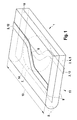
- FIG. 1 1 shows a line arrangement 1 with two electrical conductors 2 guided essentially in parallel.
- the electrical conductors 2 are applied on one side to a substrate 3 which is designed as an electrically nonconductive conductor substrate 4 and as a flexible substrate 5.
- Each of the two conductors 2 has an S-shaped configuration 6, wherein the two conductors 2 and the S-shaped formations 6 are aligned in a plane-parallel arrangement of the two conductors 2 on a flat, so not yet flattened or folded substrate 3, in the same direction.
- the two conductors 2 have in the plane-parallel, that is not folded state of the substrate 3, therefore, substantially the same distance from each other over their course.
- the substrate 3 is folded or folded at a fold 8 in such a manner that the two conductors 2 come into opposition to each other, such that their S-shaped formations 6 are superposed so that the two conductors 2 before and after the trained crossover 7 in their course are mutually aligned.
- a folding 11 takes place at the fold 8 in such a manner that a conductor side 9 of the substrate 3 is turned outward, that is, a direct, planar abutment of the substrate 3 after the folding 11 can take place without the conductors 2 touch electrically.
- the conductors 2 may be coated with an electrically non-conductive layer, so that a fold 11 can be made at the fold 8 in the opposite direction, such that the conductor sides 9 are directly opposite, that is, exactly different than in FIG FIG. 1 shown.
- the substrate 3 is a double-layered substrate 10, wherein between two superimposed layers of the double-layered substrate 10, the conductor 2 above and are guided on the underside by the layers of the substrate 3 isolated.
- the conductors 2 then in any case can not touch electrically in an undesirable manner, especially not in the region of the crossover 7.
- the conductors 2 are formed as traces 12, such a wiring is particularly simple and cost-effective possible.
- the crossover 7 lies at least approximately in the middle of the electrical length 13 in order to achieve the greatest possible decoupling of the conductors 2 from the environment. Due to the folding 11, the overlap 14 of the two conductors 2, namely the conductor tracks 12, required for forming the crossover 7 takes place.
- the two conductors 2 are partially performed in parallel and formed as punched grid tracks 15 of a stamped grid 16.
- the conductors 2 are guided in parallel in sections 17, wherein the sections 17 are interrupted only by the crossover 7.
- the crossover 7 is achieved in this embodiment so that the crossover 7 has at least one separate, electrically connected conductor element 18 as a bridge element 27, wherein the electrical connection takes place at connection points 19.
- One of the two conductors 2 is performed to form the crossover 7 S-shaped, and the other conductor 2, 20 led straight to the crossover, initially interrupted at the crossover and then straight again, but at the other side of the S-shaped guided conductor 2.
- connection points 19 can be produced for example by welding, which results in a cheap, easy to manufacture and high current carrying electrical connection.
- the conductor element 18 is held in the region of the crossing 7 by an electrically non-conductive support apparatus 22, wherein the support apparatus 22 is supported on the two conductors 2 at its respective opposite ends with transverse elements 23.
- the cross members 23 extend transversely to the conductors 2 and act on these, for example on the upper side; In particular, it is possible to manufacture the cross members 23 made of plastic 24 and they resiliently put on the ladder 2 so that they rest on the ladders 2 by a clamping force applied over the resilient plastic 24. Between the two transverse elements 23, a boom 25 is arranged, in particular connected to the transverse elements 23 or formed integrally with the transverse elements 23.
- the arm 25 carries the conductor element 18.
- the conductor element 18 at least partially, namely in its central portion 26, surrounded by material of the arm 25, in particular with plastic 24 is encapsulated.
- the crossover 7 is in turn formed at least substantially in the electrical center of the electrical length 13 of the conductors 2.
- FIG. 3 shows a line assembly 1 with two conductors 2, as already to FIG. 2 described, wherein the conductors 2 are formed as stamped lattice webs 15 and one of the two conductors 2 is guided S-shaped, that has an S-shaped configuration 6.
- the two conductors 2 are held by transverse elements 23 spaced from each other.
- the other conductor 20, which does not have the S-shaped configuration 6, is, as already in FIG. 2 described, guided substantially straight and interrupted, wherein a first conductor part 28 in approximately V-shaped over the longitudinal extent of the line assembly 1 also out approximately transversely and also provided with a plastic spacer 24 29 is provided.
- the first conductor part 28 has a right-angled branch 30 which extends the first conductor part 28 transversely to the axial extent of the other conductor 20.
- a right-angled branch 30 and a first rectangular extension is followed by an angled branch 31, which is designed such that at kinking / deformation in the angled branch 31 beyond this protruding, the spacer element 29 carrying conductor rest 32 as bridge element 27 on the S-shaped training 6 extends and the spacer element 29 after kinking displacement of the conductor element 32 is located approximately above the S-shaped configuration 6 to prevent unwanted contact between the two conductors 2.
- connection 35 is made to form the connection point 19, for example, as a weld point 36.
- the shift in Direction of the arrow V in the angled branch 31, in particular by cold forming such as punching thus provides from the conductor rest 32, the bridge member 27 for connecting the other conductors 20, wherein the bridge member 27 integral with the other conductor 20, namely one of the conductor pieces 21, formed and connected to the other conductor piece 21 at the connection point 19, in particular welded to the weld point 36.
Landscapes
- Engineering & Computer Science (AREA)
- Manufacturing & Machinery (AREA)
- Physics & Mathematics (AREA)
- Electromagnetism (AREA)
- Microelectronics & Electronic Packaging (AREA)
- Structure Of Printed Boards (AREA)
Abstract
Description
- Die Erfindung betrifft eine elektrische, insbesondere einer Datenübertragung dienende Leitungsanordnung mit mindestens zwei im Wesentlichen parallel geführten elektrischen Leitern.
- Datenübertragungen von beispielsweise symmetrischen Signalen werden im Regelfall in abgeschirmten und speziell hierfür ausgelegten Datenkabeln durchgeführt. Deren Konstruktion unterdrückt die Störaussendung der Nutzsignale über die induktive und kapazitive Koppelung, und bei der Störfestigkeit gegenüber anderen Störfeldern wird die induktive Komponente ebenfalls unterdrückt, wobei die kapazitive Kopplung zu einer Gleichtaktspannung auf den Leitungen führt, die mit geeigneten Eingangsschaltungen unterdrückt wird. Werden derartige Datensignale, also insbesondere symmetrische Signale wie beispielsweise CAN oder Flexray, über Stecker- und/oder Stanzgitterstrukturen geführt oder in einer anderen Weise parallel geführt, steigt die Störaussendung der Nutzsignale über die Einkoppelung zu anderen Leitungen, die Störunterdrückung gegenüber externen Störsignalen nimmt stark ab.
- Aufgabe der Erfindung ist es, eine elektrische, insbesondere einer Datenübertragung dienenden Leitungsanordnung mit mindestens zwei im Wesentlichen parallel geführten elektrischen Leitern bereitzustellen, die die genannten Nachteile vermeidet und eine sehr störsichere Datenübertragung mit hoher Störfreiheit gegenüber externen Störfeldern als auch mit einer nur geringen Aussendung eigener Störsignale ermöglicht.
- Hierzu wird eine elektrische, insbesondere einer Datenübertragung dienende Leitungsanordnung mit mindestens zwei im Wesentlichen parallel geführten elektrischen Leitern vorgeschlagen. Dabei ist vorgesehen, dass die Leiter mindestens eine Überkreuzung besitzen. In zweidimensionalen elektrischen Verbindungen, wie beispielsweise Stanzgittern, Leiterplatten oder auch Flexible Printed Circuits, ergeben sich die oben erwähnten nachteiligen Erscheinungen aus Koppelungen der beiden Leiter gegenüber der Umgebung. Wird aber an mindestens einer Stelle der Leiterführung eine Überkreuzung der beiden Leiter vorgesehen, hebt sich die Koppelung der beiden Leiter gegenüber der Umgebung praktisch vollständig auf. Die Überkreuzung befindet sich hierbei zur maximalen Wirksamkeit an der elektrischen Mitte der Parallelführung der beiden elektrischen Leiter, also mittig der hier betrachteten Parallelführung der beiden elektrischen Leiter. Verlaufen diese also beispielsweise für eine bestimmte Strecke s parallel (nämlich der elektrischen Länge), ist die Mitte der Überkreuzung zur maximalen Wirksamkeit bei s/2. Sind mehrere Überkreuzungen auf die elektrische Länge verteilt vorgesehen, so sind diese bevorzugt gleichmäßig beabstandet und verteilt.
- In einer weiteren Ausführungsform weist die Überkreuzung mindestens ein separates, elektrisch verbundenes Leiterelement auf. Die Überkreuzung wird so ausgeführt, dass eine Unterbrechung eines der Leiter bei Anordnungsversatz erfolgt. Um die Leiter in der Überkreuzung in der gewünschten Art und Weise elektrisch verbunden zu halten, wird mindestens ein separates, elektrisch verbundenes Leiterelement verwendet.
- In einer Ausführungsform sind die Leiter als Leiterbahnen ausgebildet. Unter Leiterbahnen werden hier im weitesten Sinne alle auf einem Substrat unmittelbar aufliegenden Leiter verstanden, beispielsweise Kupferleiterbahnen auf einer Platine.
- In einer weiteren, bevorzugten Ausführungsform sind die Leiter auf einem flexiblen Substrat ausgebildet. Als flexibles Substrat kommt beispielsweise eine Folie in Betracht, auf der die Leiter aufgebracht sind.
- Besonders bevorzugt erfolgt die Überkreuzung durch eine S-förmige Ausbildung der Leiter und eine durch Faltung des Substrats erfolgende, zumindest bereichsweise Überdeckung der Leiter im Bereich der S-förmigen Ausbildung. Diese Ausführungsform ist bei Aufbringung der Leiter auf einem flexiblen Substrat besonders vorteilhaft, da sie durch eine entsprechende Anordnung der Leiter, wie beschrieben in S-förmiger Ausbildung, und durch einfache Faltung des flexiblen Substrats ermöglicht wird. Die Faltung muss hierbei nicht eine Aufeinanderlage der Substratflächen oder Substratteile bewirken, sondern diese können auch beabstandet liegen; wesentlich ist allein, dass die S-förmige Ausbildung der Leiter in entsprechende Gegenüberlage kommt, um die Überkreuzung auszubilden (die sich beispielsweise als Projektion durch beide, gefaltete Substratflächen ergibt).
- In einer anderen Ausführungsform sind die Leiter als Stanzgitterbahnen ausgebildet. Stanzgitter finden zur Übertragung von teilweise auch hohen Strömen insbesondere in der Automobiltechnik Anwendung. Bevorzugt ist es hierbei möglich, über solche Stanzgitterbahnen auch Datensignale zu übertragen, wobei die Übertragung von Datensignalen gleichzeitig zu einer Betriebsspannungsversorgung von elektrischen Bauteilen des Fahrzeugs erfolgen kann. Insbesondere lassen sich auf diese Weise separate Datenleitungen einsparen.
- In einer weiteren Ausführungsform befindet sich die Leiter auf einem elektrisch nicht leitfähigen Leitersubstrat. Die Leiter sind demzufolge nicht vollständig isoliert, sondern liegen in mehr oder minder unisolierter Form auf dem Leitersubstrat vor, wobei sie von dem Leitersubstrat gehalten und gegeneinander isoliert werden.
- In einer Ausführungsform ist einer der Leiter zur Ausbildung der Überkreuzung S-förmig geführt und der andere Leiter bis zur Überkreuzung gerade geführt. Ab der Überkreuzung ist der andere Leiter wiederum gerade geführt, wobei mindestens ein Brückenelement, vorzugsweise ein separates Leiterelement, die beiden gerade geführten Leiterstücke schräg verlaufend miteinander verbindet, und dieses schräg verlaufende, separate Leiterelement im S-Bereich des einen Leiters geführt, mit dem einen Leiter aber nicht elektrisch verbunden ist. Die Überkreuzung wird demzufolge derart durchgeführt, dass der eine Leiter S-förmig geführt ist, während der andere Leiter gerade geführt, aber im S-Bereich des einen Leiters unterbrochen ist. Bevorzugt ist der S-förmig geführte Leiter derart geführt, dass er nach Verlassen seines S-Bereichs mit dem unterbrochenen, gerade geführten anderen Leiter fluchtet. Die beiden unterbrochenen, gerade geführten, anderen Leiter liegen demzufolge einmal links, einmal rechts des S-Bereichs. Diese beiden gerade geführten, anderen Leiterstücke werden mittels des separaten Leiterelements leitend miteinander verbunden, wobei aber das separate Leiterelement mit dem S-förmig geführten einen Leiter nicht elektrisch verbunden ist.
- Das separate Leiterelement ist mittels eines elektrisch nicht leitenden Stützapparates an mindestens einem der Leiter gehalten. Der Stützapparat dient folglich dem Halten des separaten Leiterelements. Der Stützapparat ist hierbei mindestens einem der Leiter zugeordnet.
- In einer weiteren Ausführungsform ist das separate Leiterelement mit den Leiterstücken elektrisch verbunden, insbesondere verschweißt. Selbstverständlich kommen auch andere Arten der Verbindung in Betracht, insbesondere solche, die sich leicht und kostengünstig herstellen lassen und nur eine kurze Prozesszeit benötigen, wie beispielsweise Nieten, Verpressen, Verlöten.
- In einer weiteren Ausführungsform weist der Stützapparat mindestens ein Querelement auf, das sich an den beiden Leitern mit Abstand zur Überkreuzung abstützt, wobei von dem Querelement ein Ausleger ausgeht, an dem das separate Leiterelement befestigt ist. Der Stützapparat stützt sich folglich über sein Querelement an den beiden Leitern dergestalt ab, dass das Querelement mit Abstand zur Überkreuzung liegt. Von diesem Querelement geht der Ausleger raus, an dem das separate Leiterelement befestigt ist. Das separate Leiterelement wird folglich von dem Ausleger gehalten. Der Ausleger wiederum wird vom Querelement gehalten, das sich an den Leitern abstützt beziehungsweise auf diesen hält, beispielsweise mittels einer Klemmung. Eine solche Befestigungsweise ist schnell und kostengünstig herstellbar.
- In einer weiteren Ausführungsform ist der Stützapparat oder zumindest ein Abschnitt desselben im Kunststoffspritzverfahren, insbesondere im Kunststoffumspritzverfahren, erstellt. Der Stützapparat ist aus Kunststoff sehr leicht und kostengünstig herstellbar. Er kann hierbei eine solche Ausgestaltung aufweisen, in der er als Kunststoffbauteil mindestens einen, vorzugsweise beide Leiter umgreift, beispielsweise klemmend beaufschlagt und sich so an den Leitern abstützt. Er kann auch in einer solchen Weise hergestellt sein, dass er im Kunststoffumspritzverfahren um die Leiter herum aufgespritzt ist. Es lässt sich hierdurch eine definierte, vorgegebene Anordnung der Leiter bereits durch das Umspritzen oder abschnittsweise Umspritzen zur Ausbildung des Stützapparates erzielen.
- In einer der Ausführungsformen ist das Brückenelement einstückig mit einem der beiden gerade geführten Leiterstücke ausgebildet. Dieses eine Leiterstück wird demzufolge in einer solchen Art und Weise ausgebildet, dass sich die Ausführung der Überkreuzung durch Übereinanderlegen des anderen Leiters und des einen Leiters ergibt, wobei die Leiter beabstandet zueinander liegen. Zur Sicherstellung dieser Beabstandung kann der Stützapparat oder ein Stützbeziehungsweise Isolierelement insbesondere im Bereich der Überkreuzung eingebracht werden, vorzugsweise in einer solchen Art und Weise, dass sich beide Leiter im Bereich der Überkreuzung daran abstützen.
- Weitere vorteilhafte Ausführungsformen ergeben sich aus den Unteransprüchen und aus Kombinationen selben.
- Die Erfindung wird nachfolgend anhand von Ausführungsbeispielen näher erläutert, ohne aber hierauf beschränkt zu sein.
- Es zeigen
- Figur 1
- eine Überkreuzung zweier Leiter, die auf einem flexiblen Substrat ausgebildet sind,
- Figur 2
- eine Stanzgitteranordnung mit zwei Leitern, einer Überkreuzung mit einem separaten Leiterelement als Brückenelement und einem dieses haltenden Stützapparat und
- Figur 3
- eine Stanzgitteranordnung mit einem durch Verlagerung verbundenen, einstückig zu einem gerade geführten Leiterstück ausgebildeten Brückenelement.
-
Figur 1 zeigt eine Leitungsanordnung 1 mit zwei im Wesentlichen parallel geführten elektrischen Leitern 2. Die elektrischen Leiter 2 sind auf einem Substrat 3 einseitig aufgebracht, das als elektrisch nicht leitfähiges Leitersubstrat 4 und als flexibles Substrat 5 ausgebildet ist. Jeder der beiden Leiter 2 weist eine S-förmige Ausbildung 6 auf, wobei die beiden Leiter 2 und die S-förmigen Ausbildungen 6 bei planparalleler Anordnung der beiden Leiter 2 auf ebenem, also noch nicht geklapptem oder gefaltetem Substrat 3, gleichsinnig ausgerichtet sind. Die beiden Leiter 2 weisen im planparallelen, also nicht gefalteten Zustand des Substrats 3, demnach im Wesentlichen denselben Abstand zueinander über ihren Verlauf auf. Zur Ausbildung einer Überkreuzung 7 wird das Substrat 3 in einer solchen Art und Weise an einer Faltstelle 8 gefaltet beziehungsweise geknickt, dass die beiden Leiter 2 in Gegenüberlage zueinander kommen, dergestalt, dass ihre S-förmigen Ausbildungen 6 so übereinander liegen, dass die beiden Leiter 2 vor und nach der ausgebildeten Überkreuzung 7 in ihrem Verlauf wechselseitig fluchten. Vorzugsweise erfolgt eine Faltung 11 an der Faltstelle 8 in einer solchen Art und Weise, dass eine Leiterseite 9 des Substrats 3 nach außen gekehrt wird, also eine direkte, plane Aneinanderlage des Substrats 3 nach der Faltung 11 erfolgen kann, ohne dass sich die Leiter 2 elektrisch berühren. Kumulativ oder alternativ hierzu können die Leiter 2 mit einer elektrisch nicht leitenden Schicht überzogen sein, so dass auch eine Faltung 11 an der Faltstelle 8 in entgegengesetzter Richtung vorgenommen werden kann, dergestalt, dass Leiterseiten 9 sich direkt gegenüberliegen, also genau anders als inFigur 1 dargestellt. Besonders bevorzugt ist das Substrat 3 ein doppellagiges Substrat 10, wobei zwischen zwei unmittelbar aufeinander liegenden Lagen des doppellagigen Substrats 10 die Leiter 2 ober- und unterseitig durch die Lagen des Substrats 3 isoliert geführt sind. Bei einer so erfolgenden Faltung 11 können sich die Leiter 2 dann in keinem Fall in unerwünschter Weise elektrisch berühren, insbesondere nicht im Bereich der Überkreuzung 7. Gerade in Fällen, in denen die Leiter 2 als Leiterbahnen 12 ausgebildet sind, ist eine solche Leitungsführung besonders einfach und kostengünstig möglich. Hinsichtlich einer elektrischen Länge 13 der Leiter 2 im zu betrachtenden, im Wesentlichen parallel geführten Abschnitt liegt die Überkreuzung 7 zumindest in etwa mittig der elektrischen Länge 13, um die größtmögliche Entkoppelung der Leiter 2 von der Umgebung zu erreichen. Durch die Faltung 11 erfolgt die zur Ausbildung der Überkreuzung 7 erforderliche Überdeckung 14 der beiden Leiter 2, nämlich der Leiterbahnen 12. - In einer anderen Ausführungsform, wie sie aus
Figur 2 ersichtlich ist, sind die beiden Leiter 2 abschnittsweise parallel geführt und als Stanzgitterbahnen 15 eines Stanzgitters 16 ausgebildet. Die Leiter 2 sind hierbei in Abschnitten 17 parallel geführt, wobei die Abschnitte 17 lediglich von der Überkreuzung 7 unterbrochen werden. Die Überkreuzung 7 wird in dieser Ausführungsform so erzielt, dass die Überkreuzung 7 mindestens ein separates, elektrisch verbundenes Leiterelement 18 als Brückenelement 27 aufweist, wobei die elektrische Verbindung an Verbindungsstellen 19 erfolgt. Einer der beiden Leiter 2 ist zur Ausbildung der Überkreuzung 7 S-förmig geführt, und der andere Leiter 2, 20 bis zur Überkreuzung gerade geführt, an der Überkreuzung zunächst unterbrochen und danach wieder gerade geführt, allerdings an der nun anderen Seite des S-förmig geführten Leiters 2. Hierdurch bilden sich an dem gerade geführten Leiter 2 Leiterstücke 21 aus, die im Bereich der Überkreuzung 7 unterbrochen und durch das Leiterelement 18 über die Verbindungsstelle 19 wieder elektrisch verbunden sind. Die Verbindungsstellen 19 können beispielsweise durch Verschweißung hergestellt werden, was eine billige, leicht herzustellende und hoch stromtragfähige elektrische Verbindung ergibt. Das Leiterelement 18 ist im Bereich der Überkreuzung 7 von einem elektrisch nicht leitenden Stützapparat 22 gehalten, wobei sich der Stützapparat 22 an den beiden Leitern 2 an seinen sich jeweils gegenüberliegenden Enden mit Querelementen 23 abstützt. Die Querelemente 23 verlaufen quer zu den Leitern 2 und beaufschlagen diese beispielsweise oberseitig; insbesondere ist es möglich, die Querelemente 23 aus Kunststoff 24 zu fertigen und sie federnd auf die Leiter 2 aufzustecken, so dass sie sich auf den Leitern 2 durch eine über den federnden Kunststoff 24 aufgebrachte Klemmkraft halten. Zwischen den beiden Querelementen 23 ist ein Ausleger 25 angeordnet, insbesondere mit den Querelementen 23 verbunden oder einstückig zu den Querelementen 23 ausgebildet. Der Ausleger 25 trägt das Leiterelement 18. Insbesondere ist vorgesehen, dass das Leiterelement 18 zumindest abschnittsweise, nämlich in seinem Mittelabschnitt 26, von Material des Auslegers 25 umgegeben, insbesondere mit Kunststoff 24 umspritzt ist. Die Überkreuzung 7 ist wiederum zumindest im Wesentlichen in der elektrischen Mitte der elektrischen Länge 13 der Leiter 2 ausgebildet. -
Figur 3 zeigt eine Leitungsanordnung 1 mit zwei Leitern 2, wie bereits zuFigur 2 beschrieben, wobei die Leiter 2 als Stanzgitterbahnen 15 ausgebildet sind und einer der beiden Leiter 2 S-förmig geführt ist, also eine S-förmige Ausbildung 6 aufweist. Die beiden Leiter 2 werden durch Querelemente 23 beabstandet voneinander gehalten. Der andere Leiter 20, der nicht die S-förmige Ausbildung 6 aufweist, ist, wie bereits inFigur 2 beschrieben, im Wesentlichen gerade geführt und unterbrochen, wobei ein erster Leiterteil 28 in etwa V-förmig über die Längserstreckung der Leitungsanordnung 1 hinaus annähernd quer geführt und ebenfalls mit einem aus Kunststoff 24 bestehenden Distanzelement 29 versehen ist. Der erste Leiterteil 28 weist eine rechtwinklige Abzweigung 30 auf, die den ersten Leiterteil 28 quer zur Axialerstreckung des anderen Leiters 20 erstreckt. An diese rechtwinklige Abzweigung 30 und eine erste rechtwinklige Erstreckung anschließend folgt eine winklige Abzweigung 31, die dergestalt ausgebildet ist, dass bei Abknicken/Verformen in der winkligen Abzweigung 31 der über diese hinaus ragende, das Distanzelement 29 tragende Leiterrest 32 als Brückenelement 27 sich über die S-förmige Ausbildung 6 erstreckt und das Distanzelement 29 nach abknickender Verlagerung des Leiterelements 32 in etwa über der S-förmigen Ausbildung 6 liegt, um einen unerwünschten Berührkontakt zwischen den beiden Leitern 2 zu verhindern. In einem Leiterendbereich 33 des Leiterrests 32, der auf einem Verbindungsbereich 34 des gerade geführten anderen Leiters 20 in Gegenüberlage der S-förmigen Ausbildung 6 liegt, erfolgt nach dem Umformen/Verlagern des Leiterrests 32 zur Ausbildung des Brückenelements 27 eine Verbindung 35 unter Herstellung der Verbindungsstelle 19, beispielsweise als Schweißpunkt 36. Die Verlagerung in Richtung des Pfeils V in der winkligen Abzweigung 31, insbesondere durch Kaltverformen wie etwa Stanzen, stellt somit aus dem Leiterrest 32 das Brückenelement 27 zur Verbindung der anderen Leiter 20 zur Verfügung, wobei das Brückenelement 27 einstückig mit dem anderen Leiter 20, nämlich einem der Leiterstücke 21, ausgebildet und mit dem anderen Leiterstück 21 an der Verbindungsstelle 19 verbunden, insbesondere über den Schweißpunkt 36 verschweißt ist.
Claims (15)
- Elektrische, insbesondere einer Datenübertragung dienende Leitungsanordnung mit mindestens zwei im Wesentlichen parallel geführten elektrischen Leitern, dadurch gekennzeichnet, dass die Leiter (2) mindestens eine Überkreuzung (7) besitzen.
- Leitungsanordnung nach Anspruch 1, dadurch gekennzeichnet, dass die Überkreuzung in oder im Wesentlichen in einer elektrischen Mitte einer elektrischen Länge (13) der Leiter (2) ausgebildet ist.
- Leitungsanordnung nach einem der vorhergehenden Ansprüche, dadurch gekennzeichnet, dass die Überkreuzung (7) mindestens ein separates, elektrisch verbundenes Leiterelement (18) aufweist.
- Leitungsanordnung nach einem der vorhergehenden Ansprüche, dadurch gekennzeichnet, dass die Leiter (2) als Leiterbahnen (12) ausgebildet sind.
- Leitungsanordnung nach einem der vorhergehenden Ansprüche, dadurch gekennzeichnet, dass die Leiter (2) auf einem flexiblen Substrat (5) ausgebildet sind.
- Leitungsanordnung nach einem der vorhergehenden Ansprüche, dadurch gekennzeichnet, dass die Überkreuzung (7) durch eine S-förmige Ausbildung (6) der Leiter (2) und eine durch Faltung (11) des Substrats (3) erfolgende, zumindest bereichsweise Überdeckung (14) der Leiter (2) im Bereich der S-förmigen Ausbildung (6) erfolgt.
- Leitungsanordnung nach einem der vorhergehenden Ansprüche, dadurch gekennzeichnet, dass die Leiter (2) als Stanzgitterbahnen (15) ausgebildet sind.
- Leitungsanordnung nach einem der vorhergehenden Ansprüche, dadurch gekennzeichnet, dass sich die Leiter (2) auf einem elektrisch nicht leitfähigen Leitersubstrat (4) befinden.
- Leitungsanordnung nach einem der vorhergehenden Ansprüche, dadurch gekennzeichnet, dass einer der Leiter (2) zur Ausbildung der Überkreuzung (7) S-förmig geführt ist und dass der andere Leiter (2,20) bis zur Überkreuzung (7) gerade geführt und ab der Überkreuzung (7) wiederum gerade geführt ist und dass mindestens ein Brückenelement (27), vorzugsweise ein separates Leiterelement (18), die beiden gerade geführten Leiterstücke (21) schräg verlaufend im S-Bereich des einen Leiters (2) verbindet und mit dem einen Leiter (2) elektrisch nicht verbunden ist.
- Leitungsanordnung nach einem der vorhergehenden Ansprüche, dadurch gekennzeichnet, dass das separate Leiterelement (18) mittels eines elektrisch nicht leitenden Stützapparats (22) an mindestens einem der Leiter (2,20) gehalten ist.
- Leitungsanordnung nach einem der vorhergehenden Ansprüche, dadurch gekennzeichnet, dass das separate Leiterelement (18) mit den Leiterstücken (21) elektrisch verbunden, insbesondere verschweißt, ist.
- Leitungsanordnung nach einem der vorhergehenden Ansprüche, dadurch gekennzeichnet, dass der Stützapparat (22) mindestens ein Querelement (23) aufweist, das sich an den beiden Leitern (2,20) mit Abstand zur Überkreuzung (7) abstützt, wobei von dem Querelement (23) ein Ausleger (25) ausgeht, an dem das separate Leiterelement (18) befestigt ist.
- Leitungsanordnung nach einem der vorhergehenden Ansprüche, dadurch gekennzeichnet, dass der Stützapparat (22) oder zumindest ein Abschnitt (17) davon im Kunststoffspritzverfahren, insbesondere im Kunststoffumspritzverfahren, erstellt ist.
- Leitungsanordnung nach einem der vorhergehenden Ansprüche, dadurch gekennzeichnet, dass das Brückenelement (27) einstückig mit einem der beiden gerade geführten Leiterstücke (21) ausgebildet und zur Ausbildung der Überkreuzung (7) verformt und zumindest abschnittsweise verlagert ist.
- Leitungsanordnung nach einem der vorhergehenden Ansprüche, dadurch gekennzeichnet, dass die Verlagerung des Brückenelements (27) durch einen Umformungsvorgang, insbesondere eine Kaltverformung, bewirkt ist.
Applications Claiming Priority (1)
| Application Number | Priority Date | Filing Date | Title |
|---|---|---|---|
| DE200810042845 DE102008042845A1 (de) | 2008-10-15 | 2008-10-15 | Elektrische Leitungsanordnung |
Publications (2)
| Publication Number | Publication Date |
|---|---|
| EP2178154A1 true EP2178154A1 (de) | 2010-04-21 |
| EP2178154B1 EP2178154B1 (de) | 2013-05-22 |
Family
ID=41402228
Family Applications (1)
| Application Number | Title | Priority Date | Filing Date |
|---|---|---|---|
| EP20090172550 Not-in-force EP2178154B1 (de) | 2008-10-15 | 2009-10-08 | Elektrische Leitungsanordnung |
Country Status (2)
| Country | Link |
|---|---|
| EP (1) | EP2178154B1 (de) |
| DE (1) | DE102008042845A1 (de) |
Families Citing this family (1)
| Publication number | Priority date | Publication date | Assignee | Title |
|---|---|---|---|---|
| DE102021201446A1 (de) | 2021-02-16 | 2022-08-18 | Robert Bosch Gesellschaft mit beschränkter Haftung | Leitungsanordnung und Steuergerät mit einer Leitungsanordnung |
Citations (6)
| Publication number | Priority date | Publication date | Assignee | Title |
|---|---|---|---|---|
| FR1402897A (fr) * | 1964-03-06 | 1965-06-18 | Telecommunications Sa | Circuits à conducteurs plats pour câbles de télécommunication |
| EP0809260A2 (de) * | 1996-05-24 | 1997-11-26 | Molex Incorporated | Biegsames Flachkabel mit pseudo-verdrillten Leitern |
| DE19738754A1 (de) * | 1997-09-04 | 1999-03-11 | Delphi Automotive Systems Gmbh | Abgeschirmte elektrische Drähte |
| JP2001236479A (ja) * | 2000-02-22 | 2001-08-31 | Miyota Kk | 非接触型icカード |
| WO2006036689A1 (en) * | 2004-09-24 | 2006-04-06 | Storage Technology Corporation | System and method for crosstalk reduction in a flexible trace interconnect array |
| EP2068391A2 (de) * | 2007-12-04 | 2009-06-10 | Rohde & Schwarz GmbH & Co. KG | Einrichtung mit überkreutzter Streifenleitung |
-
2008
- 2008-10-15 DE DE200810042845 patent/DE102008042845A1/de not_active Withdrawn
-
2009
- 2009-10-08 EP EP20090172550 patent/EP2178154B1/de not_active Not-in-force
Patent Citations (6)
| Publication number | Priority date | Publication date | Assignee | Title |
|---|---|---|---|---|
| FR1402897A (fr) * | 1964-03-06 | 1965-06-18 | Telecommunications Sa | Circuits à conducteurs plats pour câbles de télécommunication |
| EP0809260A2 (de) * | 1996-05-24 | 1997-11-26 | Molex Incorporated | Biegsames Flachkabel mit pseudo-verdrillten Leitern |
| DE19738754A1 (de) * | 1997-09-04 | 1999-03-11 | Delphi Automotive Systems Gmbh | Abgeschirmte elektrische Drähte |
| JP2001236479A (ja) * | 2000-02-22 | 2001-08-31 | Miyota Kk | 非接触型icカード |
| WO2006036689A1 (en) * | 2004-09-24 | 2006-04-06 | Storage Technology Corporation | System and method for crosstalk reduction in a flexible trace interconnect array |
| EP2068391A2 (de) * | 2007-12-04 | 2009-06-10 | Rohde & Schwarz GmbH & Co. KG | Einrichtung mit überkreutzter Streifenleitung |
Also Published As
| Publication number | Publication date |
|---|---|
| DE102008042845A1 (de) | 2010-04-22 |
| EP2178154B1 (de) | 2013-05-22 |
Similar Documents
| Publication | Publication Date | Title |
|---|---|---|
| WO2011141314A1 (de) | Tragschienenbussystem | |
| DE112012001747T5 (de) | Stromanschlussschiene für die Verwendung in einem Elektromotor | |
| DE102017215419A1 (de) | Kondensatoreinheit und Baugruppe für eine Leistungselektronik | |
| DE102004006575A1 (de) | Leistungsverteiler für ein Kraftfahrzeug | |
| DE102018104843A1 (de) | Erdungsanschlusselement zur Abschirmung von in Kunststoffgehäusen angeordneten elektrischen Komponenten sowie Verfahren zu seinem Einbau | |
| EP3010095B1 (de) | Einpresskontakt | |
| EP2178154B1 (de) | Elektrische Leitungsanordnung | |
| DE102016002821A1 (de) | Schaltkreis einer elektronischen Steuereinheit | |
| DE202013010951U1 (de) | Baugruppe zur Leiterplattenbestückung | |
| DE112018005377B4 (de) | Mit einem Anschluss ausgerüsteter Draht | |
| DE102013013715B4 (de) | Elektrische Kontaktanordnung sowie Verfahren zum Herstellen einer solchen elektrischen Kontaktanordnung | |
| EP3469664A1 (de) | Leitungsintegrierter halbleiterschalter und verfahren zu dessen herstellung | |
| DE2056909C3 (de) | Verfahren zur Herstellung von kunststoffumhüllten Spulen | |
| DE102007003652B4 (de) | Elektrische Überbrückung | |
| EP4282034B1 (de) | Stromverbindungsvorrichtung für leiterplatten und verfahren zur montage einer derartigen stromverbindungsvorrichtung an einer leiterplatte | |
| DE102015106518A1 (de) | Elektrisches Bauteil | |
| DE102014224933A1 (de) | Bauelement-Steckverbindungsanordnung zum steckbaren Verbinden eines Bauelements mit einer Leiterplatte und Verfahren zur Herstellung einer derartigen Bauelement-Steckverbindungsanordnung | |
| DE202011109444U1 (de) | Kontaktelement | |
| DE4238867C2 (de) | Vorrichtung und Verfahren zum Anschließen von mehreren elektrischen Verbrauchern | |
| DE102016206042A1 (de) | Stromverteiler für ein Fahrzeugbordnetz und zugehöriges Fahrzeugbordnetz | |
| DE19948454A1 (de) | Folienleiter mit einem einem Gegenstück definiert zuzuordnenden Kopplungsbereich | |
| DE102012223077A1 (de) | Kontaktanordnung für einen mehrlagigen Schaltungsträger | |
| DE102011078740A1 (de) | Adapterelement zum Verbinden eines Kfz-Kabelbaumes mit einem Flachbandkabel | |
| EP3745562B1 (de) | Spulenkörper mit integrierter kontaktiervorrichtung | |
| WO2025190581A1 (de) | Abschirmelement |
Legal Events
| Date | Code | Title | Description |
|---|---|---|---|
| PUAI | Public reference made under article 153(3) epc to a published international application that has entered the european phase |
Free format text: ORIGINAL CODE: 0009012 |
|
| AK | Designated contracting states |
Kind code of ref document: A1 Designated state(s): AT BE BG CH CY CZ DE DK EE ES FI FR GB GR HR HU IE IS IT LI LT LU LV MC MK MT NL NO PL PT RO SE SI SK SM TR |
|
| AX | Request for extension of the european patent |
Extension state: AL BA RS |
|
| 17P | Request for examination filed |
Effective date: 20101021 |
|
| 17Q | First examination report despatched |
Effective date: 20101112 |
|
| GRAP | Despatch of communication of intention to grant a patent |
Free format text: ORIGINAL CODE: EPIDOSNIGR1 |
|
| GRAS | Grant fee paid |
Free format text: ORIGINAL CODE: EPIDOSNIGR3 |
|
| GRAA | (expected) grant |
Free format text: ORIGINAL CODE: 0009210 |
|
| AK | Designated contracting states |
Kind code of ref document: B1 Designated state(s): AT BE BG CH CY CZ DE DK EE ES FI FR GB GR HR HU IE IS IT LI LT LU LV MC MK MT NL NO PL PT RO SE SI SK SM TR |
|
| REG | Reference to a national code |
Ref country code: GB Ref legal event code: FG4D Free format text: NOT ENGLISH |
|
| REG | Reference to a national code |
Ref country code: CH Ref legal event code: EP |
|
| REG | Reference to a national code |
Ref country code: AT Ref legal event code: REF Ref document number: 613648 Country of ref document: AT Kind code of ref document: T Effective date: 20130615 |
|
| REG | Reference to a national code |
Ref country code: IE Ref legal event code: FG4D Free format text: LANGUAGE OF EP DOCUMENT: GERMAN |
|
| REG | Reference to a national code |
Ref country code: DE Ref legal event code: R096 Ref document number: 502009007148 Country of ref document: DE Effective date: 20130718 |
|
| REG | Reference to a national code |
Ref country code: LT Ref legal event code: MG4D |
|
| PG25 | Lapsed in a contracting state [announced via postgrant information from national office to epo] |
Ref country code: ES Free format text: LAPSE BECAUSE OF FAILURE TO SUBMIT A TRANSLATION OF THE DESCRIPTION OR TO PAY THE FEE WITHIN THE PRESCRIBED TIME-LIMIT Effective date: 20130902 Ref country code: IS Free format text: LAPSE BECAUSE OF FAILURE TO SUBMIT A TRANSLATION OF THE DESCRIPTION OR TO PAY THE FEE WITHIN THE PRESCRIBED TIME-LIMIT Effective date: 20130922 Ref country code: LT Free format text: LAPSE BECAUSE OF FAILURE TO SUBMIT A TRANSLATION OF THE DESCRIPTION OR TO PAY THE FEE WITHIN THE PRESCRIBED TIME-LIMIT Effective date: 20130522 Ref country code: FI Free format text: LAPSE BECAUSE OF FAILURE TO SUBMIT A TRANSLATION OF THE DESCRIPTION OR TO PAY THE FEE WITHIN THE PRESCRIBED TIME-LIMIT Effective date: 20130522 Ref country code: NO Free format text: LAPSE BECAUSE OF FAILURE TO SUBMIT A TRANSLATION OF THE DESCRIPTION OR TO PAY THE FEE WITHIN THE PRESCRIBED TIME-LIMIT Effective date: 20130822 Ref country code: SI Free format text: LAPSE BECAUSE OF FAILURE TO SUBMIT A TRANSLATION OF THE DESCRIPTION OR TO PAY THE FEE WITHIN THE PRESCRIBED TIME-LIMIT Effective date: 20130522 Ref country code: GR Free format text: LAPSE BECAUSE OF FAILURE TO SUBMIT A TRANSLATION OF THE DESCRIPTION OR TO PAY THE FEE WITHIN THE PRESCRIBED TIME-LIMIT Effective date: 20130823 Ref country code: SE Free format text: LAPSE BECAUSE OF FAILURE TO SUBMIT A TRANSLATION OF THE DESCRIPTION OR TO PAY THE FEE WITHIN THE PRESCRIBED TIME-LIMIT Effective date: 20130522 Ref country code: PT Free format text: LAPSE BECAUSE OF FAILURE TO SUBMIT A TRANSLATION OF THE DESCRIPTION OR TO PAY THE FEE WITHIN THE PRESCRIBED TIME-LIMIT Effective date: 20130923 |
|
| REG | Reference to a national code |
Ref country code: NL Ref legal event code: VDEP Effective date: 20130522 |
|
| PG25 | Lapsed in a contracting state [announced via postgrant information from national office to epo] |
Ref country code: PL Free format text: LAPSE BECAUSE OF FAILURE TO SUBMIT A TRANSLATION OF THE DESCRIPTION OR TO PAY THE FEE WITHIN THE PRESCRIBED TIME-LIMIT Effective date: 20130522 Ref country code: BG Free format text: LAPSE BECAUSE OF FAILURE TO SUBMIT A TRANSLATION OF THE DESCRIPTION OR TO PAY THE FEE WITHIN THE PRESCRIBED TIME-LIMIT Effective date: 20130822 Ref country code: HR Free format text: LAPSE BECAUSE OF FAILURE TO SUBMIT A TRANSLATION OF THE DESCRIPTION OR TO PAY THE FEE WITHIN THE PRESCRIBED TIME-LIMIT Effective date: 20130522 |
|
| PG25 | Lapsed in a contracting state [announced via postgrant information from national office to epo] |
Ref country code: LV Free format text: LAPSE BECAUSE OF FAILURE TO SUBMIT A TRANSLATION OF THE DESCRIPTION OR TO PAY THE FEE WITHIN THE PRESCRIBED TIME-LIMIT Effective date: 20130522 |
|
| PG25 | Lapsed in a contracting state [announced via postgrant information from national office to epo] |
Ref country code: CZ Free format text: LAPSE BECAUSE OF FAILURE TO SUBMIT A TRANSLATION OF THE DESCRIPTION OR TO PAY THE FEE WITHIN THE PRESCRIBED TIME-LIMIT Effective date: 20130522 Ref country code: DK Free format text: LAPSE BECAUSE OF FAILURE TO SUBMIT A TRANSLATION OF THE DESCRIPTION OR TO PAY THE FEE WITHIN THE PRESCRIBED TIME-LIMIT Effective date: 20130522 Ref country code: EE Free format text: LAPSE BECAUSE OF FAILURE TO SUBMIT A TRANSLATION OF THE DESCRIPTION OR TO PAY THE FEE WITHIN THE PRESCRIBED TIME-LIMIT Effective date: 20130522 Ref country code: SK Free format text: LAPSE BECAUSE OF FAILURE TO SUBMIT A TRANSLATION OF THE DESCRIPTION OR TO PAY THE FEE WITHIN THE PRESCRIBED TIME-LIMIT Effective date: 20130522 |
|
| PG25 | Lapsed in a contracting state [announced via postgrant information from national office to epo] |
Ref country code: NL Free format text: LAPSE BECAUSE OF FAILURE TO SUBMIT A TRANSLATION OF THE DESCRIPTION OR TO PAY THE FEE WITHIN THE PRESCRIBED TIME-LIMIT Effective date: 20130522 Ref country code: RO Free format text: LAPSE BECAUSE OF FAILURE TO SUBMIT A TRANSLATION OF THE DESCRIPTION OR TO PAY THE FEE WITHIN THE PRESCRIBED TIME-LIMIT Effective date: 20130522 |
|
| PLBE | No opposition filed within time limit |
Free format text: ORIGINAL CODE: 0009261 |
|
| STAA | Information on the status of an ep patent application or granted ep patent |
Free format text: STATUS: NO OPPOSITION FILED WITHIN TIME LIMIT |
|
| 26N | No opposition filed |
Effective date: 20140225 |
|
| BERE | Be: lapsed |
Owner name: ROBERT BOSCH G.M.B.H. Effective date: 20131031 |
|
| PG25 | Lapsed in a contracting state [announced via postgrant information from national office to epo] |
Ref country code: MC Free format text: LAPSE BECAUSE OF FAILURE TO SUBMIT A TRANSLATION OF THE DESCRIPTION OR TO PAY THE FEE WITHIN THE PRESCRIBED TIME-LIMIT Effective date: 20130522 |
|
| REG | Reference to a national code |
Ref country code: CH Ref legal event code: PL |
|
| REG | Reference to a national code |
Ref country code: DE Ref legal event code: R097 Ref document number: 502009007148 Country of ref document: DE Effective date: 20140225 |
|
| REG | Reference to a national code |
Ref country code: IE Ref legal event code: MM4A |
|
| PG25 | Lapsed in a contracting state [announced via postgrant information from national office to epo] |
Ref country code: LI Free format text: LAPSE BECAUSE OF NON-PAYMENT OF DUE FEES Effective date: 20131031 Ref country code: CH Free format text: LAPSE BECAUSE OF NON-PAYMENT OF DUE FEES Effective date: 20131031 |
|
| PG25 | Lapsed in a contracting state [announced via postgrant information from national office to epo] |
Ref country code: BE Free format text: LAPSE BECAUSE OF NON-PAYMENT OF DUE FEES Effective date: 20131031 |
|
| PG25 | Lapsed in a contracting state [announced via postgrant information from national office to epo] |
Ref country code: IE Free format text: LAPSE BECAUSE OF NON-PAYMENT OF DUE FEES Effective date: 20131008 |
|
| PG25 | Lapsed in a contracting state [announced via postgrant information from national office to epo] |
Ref country code: SM Free format text: LAPSE BECAUSE OF FAILURE TO SUBMIT A TRANSLATION OF THE DESCRIPTION OR TO PAY THE FEE WITHIN THE PRESCRIBED TIME-LIMIT Effective date: 20130522 |
|
| PG25 | Lapsed in a contracting state [announced via postgrant information from national office to epo] |
Ref country code: TR Free format text: LAPSE BECAUSE OF FAILURE TO SUBMIT A TRANSLATION OF THE DESCRIPTION OR TO PAY THE FEE WITHIN THE PRESCRIBED TIME-LIMIT Effective date: 20130522 Ref country code: CY Free format text: LAPSE BECAUSE OF FAILURE TO SUBMIT A TRANSLATION OF THE DESCRIPTION OR TO PAY THE FEE WITHIN THE PRESCRIBED TIME-LIMIT Effective date: 20130522 |
|
| PG25 | Lapsed in a contracting state [announced via postgrant information from national office to epo] |
Ref country code: HU Free format text: LAPSE BECAUSE OF FAILURE TO SUBMIT A TRANSLATION OF THE DESCRIPTION OR TO PAY THE FEE WITHIN THE PRESCRIBED TIME-LIMIT; INVALID AB INITIO Effective date: 20091008 Ref country code: MK Free format text: LAPSE BECAUSE OF FAILURE TO SUBMIT A TRANSLATION OF THE DESCRIPTION OR TO PAY THE FEE WITHIN THE PRESCRIBED TIME-LIMIT Effective date: 20130522 Ref country code: LU Free format text: LAPSE BECAUSE OF NON-PAYMENT OF DUE FEES Effective date: 20131008 |
|
| PG25 | Lapsed in a contracting state [announced via postgrant information from national office to epo] |
Ref country code: MT Free format text: LAPSE BECAUSE OF FAILURE TO SUBMIT A TRANSLATION OF THE DESCRIPTION OR TO PAY THE FEE WITHIN THE PRESCRIBED TIME-LIMIT Effective date: 20130522 |
|
| REG | Reference to a national code |
Ref country code: FR Ref legal event code: PLFP Year of fee payment: 7 |
|
| REG | Reference to a national code |
Ref country code: AT Ref legal event code: MM01 Ref document number: 613648 Country of ref document: AT Kind code of ref document: T Effective date: 20141008 |
|
| PG25 | Lapsed in a contracting state [announced via postgrant information from national office to epo] |
Ref country code: AT Free format text: LAPSE BECAUSE OF NON-PAYMENT OF DUE FEES Effective date: 20141008 |
|
| REG | Reference to a national code |
Ref country code: FR Ref legal event code: PLFP Year of fee payment: 8 |
|
| REG | Reference to a national code |
Ref country code: FR Ref legal event code: PLFP Year of fee payment: 9 |
|
| REG | Reference to a national code |
Ref country code: FR Ref legal event code: PLFP Year of fee payment: 10 |
|
| PGFP | Annual fee paid to national office [announced via postgrant information from national office to epo] |
Ref country code: DE Payment date: 20181206 Year of fee payment: 10 |
|
| PGFP | Annual fee paid to national office [announced via postgrant information from national office to epo] |
Ref country code: IT Payment date: 20191021 Year of fee payment: 11 Ref country code: FR Payment date: 20191022 Year of fee payment: 11 |
|
| PGFP | Annual fee paid to national office [announced via postgrant information from national office to epo] |
Ref country code: GB Payment date: 20191023 Year of fee payment: 11 |
|
| REG | Reference to a national code |
Ref country code: DE Ref legal event code: R119 Ref document number: 502009007148 Country of ref document: DE |
|
| PG25 | Lapsed in a contracting state [announced via postgrant information from national office to epo] |
Ref country code: DE Free format text: LAPSE BECAUSE OF NON-PAYMENT OF DUE FEES Effective date: 20200501 |
|
| GBPC | Gb: european patent ceased through non-payment of renewal fee |
Effective date: 20201008 |
|
| PG25 | Lapsed in a contracting state [announced via postgrant information from national office to epo] |
Ref country code: FR Free format text: LAPSE BECAUSE OF NON-PAYMENT OF DUE FEES Effective date: 20201031 |
|
| PG25 | Lapsed in a contracting state [announced via postgrant information from national office to epo] |
Ref country code: GB Free format text: LAPSE BECAUSE OF NON-PAYMENT OF DUE FEES Effective date: 20201008 |
|
| PG25 | Lapsed in a contracting state [announced via postgrant information from national office to epo] |
Ref country code: IT Free format text: LAPSE BECAUSE OF NON-PAYMENT OF DUE FEES Effective date: 20201008 |