EP2174388B1 - Electrical connector assembly - Google Patents
Electrical connector assembly Download PDFInfo
- Publication number
- EP2174388B1 EP2174388B1 EP08772121A EP08772121A EP2174388B1 EP 2174388 B1 EP2174388 B1 EP 2174388B1 EP 08772121 A EP08772121 A EP 08772121A EP 08772121 A EP08772121 A EP 08772121A EP 2174388 B1 EP2174388 B1 EP 2174388B1
- Authority
- EP
- European Patent Office
- Prior art keywords
- contact
- electrical cable
- electrical
- header
- ground
- Prior art date
- Legal status (The legal status is an assumption and is not a legal conclusion. Google has not performed a legal analysis and makes no representation as to the accuracy of the status listed.)
- Not-in-force
Links
Images


Classifications
-
- H—ELECTRICITY
- H01—ELECTRIC ELEMENTS
- H01R—ELECTRICALLY-CONDUCTIVE CONNECTIONS; STRUCTURAL ASSOCIATIONS OF A PLURALITY OF MUTUALLY-INSULATED ELECTRICAL CONNECTING ELEMENTS; COUPLING DEVICES; CURRENT COLLECTORS
- H01R13/00—Details of coupling devices of the kinds covered by groups H01R12/70 or H01R24/00 - H01R33/00
- H01R13/46—Bases; Cases
- H01R13/502—Bases; Cases composed of different pieces
- H01R13/506—Bases; Cases composed of different pieces assembled by snap action of the parts
-
- H—ELECTRICITY
- H01—ELECTRIC ELEMENTS
- H01R—ELECTRICALLY-CONDUCTIVE CONNECTIONS; STRUCTURAL ASSOCIATIONS OF A PLURALITY OF MUTUALLY-INSULATED ELECTRICAL CONNECTING ELEMENTS; COUPLING DEVICES; CURRENT COLLECTORS
- H01R13/00—Details of coupling devices of the kinds covered by groups H01R12/70 or H01R24/00 - H01R33/00
- H01R13/46—Bases; Cases
- H01R13/516—Means for holding or embracing insulating body, e.g. casing, hoods
- H01R13/518—Means for holding or embracing insulating body, e.g. casing, hoods for holding or embracing several coupling parts, e.g. frames
-
- H—ELECTRICITY
- H01—ELECTRIC ELEMENTS
- H01R—ELECTRICALLY-CONDUCTIVE CONNECTIONS; STRUCTURAL ASSOCIATIONS OF A PLURALITY OF MUTUALLY-INSULATED ELECTRICAL CONNECTING ELEMENTS; COUPLING DEVICES; CURRENT COLLECTORS
- H01R13/00—Details of coupling devices of the kinds covered by groups H01R12/70 or H01R24/00 - H01R33/00
- H01R13/646—Details of coupling devices of the kinds covered by groups H01R12/70 or H01R24/00 - H01R33/00 specially adapted for high-frequency, e.g. structures providing an impedance match or phase match
- H01R13/6461—Means for preventing cross-talk
- H01R13/6471—Means for preventing cross-talk by special arrangement of ground and signal conductors, e.g. GSGS [Ground-Signal-Ground-Signal]
-
- H—ELECTRICITY
- H01—ELECTRIC ELEMENTS
- H01R—ELECTRICALLY-CONDUCTIVE CONNECTIONS; STRUCTURAL ASSOCIATIONS OF A PLURALITY OF MUTUALLY-INSULATED ELECTRICAL CONNECTING ELEMENTS; COUPLING DEVICES; CURRENT COLLECTORS
- H01R13/00—Details of coupling devices of the kinds covered by groups H01R12/70 or H01R24/00 - H01R33/00
- H01R13/648—Protective earth or shield arrangements on coupling devices, e.g. anti-static shielding
- H01R13/658—High frequency shielding arrangements, e.g. against EMI [Electro-Magnetic Interference] or EMP [Electro-Magnetic Pulse]
- H01R13/6591—Specific features or arrangements of connection of shield to conductive members
- H01R13/6592—Specific features or arrangements of connection of shield to conductive members the conductive member being a shielded cable
- H01R13/6593—Specific features or arrangements of connection of shield to conductive members the conductive member being a shielded cable the shield being composed of different pieces
-
- H—ELECTRICITY
- H01—ELECTRIC ELEMENTS
- H01R—ELECTRICALLY-CONDUCTIVE CONNECTIONS; STRUCTURAL ASSOCIATIONS OF A PLURALITY OF MUTUALLY-INSULATED ELECTRICAL CONNECTING ELEMENTS; COUPLING DEVICES; CURRENT COLLECTORS
- H01R13/00—Details of coupling devices of the kinds covered by groups H01R12/70 or H01R24/00 - H01R33/00
- H01R13/646—Details of coupling devices of the kinds covered by groups H01R12/70 or H01R24/00 - H01R33/00 specially adapted for high-frequency, e.g. structures providing an impedance match or phase match
- H01R13/6473—Impedance matching
- H01R13/6477—Impedance matching by variation of dielectric properties
-
- H—ELECTRICITY
- H01—ELECTRIC ELEMENTS
- H01R—ELECTRICALLY-CONDUCTIVE CONNECTIONS; STRUCTURAL ASSOCIATIONS OF A PLURALITY OF MUTUALLY-INSULATED ELECTRICAL CONNECTING ELEMENTS; COUPLING DEVICES; CURRENT COLLECTORS
- H01R13/00—Details of coupling devices of the kinds covered by groups H01R12/70 or H01R24/00 - H01R33/00
- H01R13/648—Protective earth or shield arrangements on coupling devices, e.g. anti-static shielding
- H01R13/658—High frequency shielding arrangements, e.g. against EMI [Electro-Magnetic Interference] or EMP [Electro-Magnetic Pulse]
- H01R13/6581—Shield structure
- H01R13/6582—Shield structure with resilient means for engaging mating connector
-
- H—ELECTRICITY
- H01—ELECTRIC ELEMENTS
- H01R—ELECTRICALLY-CONDUCTIVE CONNECTIONS; STRUCTURAL ASSOCIATIONS OF A PLURALITY OF MUTUALLY-INSULATED ELECTRICAL CONNECTING ELEMENTS; COUPLING DEVICES; CURRENT COLLECTORS
- H01R24/00—Two-part coupling devices, or either of their cooperating parts, characterised by their overall structure
- H01R24/38—Two-part coupling devices, or either of their cooperating parts, characterised by their overall structure having concentrically or coaxially arranged contacts
- H01R24/40—Two-part coupling devices, or either of their cooperating parts, characterised by their overall structure having concentrically or coaxially arranged contacts specially adapted for high frequency
- H01R24/56—Two-part coupling devices, or either of their cooperating parts, characterised by their overall structure having concentrically or coaxially arranged contacts specially adapted for high frequency specially adapted to a specific shape of cables, e.g. corrugated cables, twisted pair cables, cables with two screens or hollow cables
Definitions
- the present invention relates generally to interconnections made between a printed circuit board and one or more electrical cables carrying signals to and from the printed circuit board.
- Connector systems developed for high-speed board-to-board and board-to-cable interconnect applications are replete in the art.
- an optimum printed circuit board interconnect design minimizes the length of marginally controlled signal line characteristic impedance by minimizing the physical spacing between the printed circuit board and the connector.
- connector designs which involve relatively large pin and socket connectors with multiple pins devoted to power and ground contacts provide only marginally acceptable performance for high speed printed circuit boards.
- US 2007141871 discloses an electrical connector assembly for transmitting high speed electrical signals, that includes a header and a carrier.
- the header has a plurality of signal pins, a plurality of ground pins, and a supplemental ground contact.
- the carrier is configured to mate with the header.
- a plurality of electrical cable terminations are retained by the carrier, and the header and cable terminations are configured such that each of the plurality of electrical cable terminations makes electrical contact with one or more of the signal pins, ground pins, and supplemental ground contact when the header and carrier are in a mated configuration.
- WO 2005109578 discloses an electrical connector that includes an insulative carrier having therein at least one cable connector.
- the carrier is configured to engage a header having a plurality of signal pins and a plurality of shield blades extending therefrom.
- Each cable connector terminates a corresponding cable and includes a conductive outer housing having an insulative inner housing.
- the inner housing holds first and second conductive terminals in electrical isolation from each other and the outer housing.
- the inner housing is configured for receiving a shield blade between the first and second terminals.
- the outer housing includes a first contact for electrically coupling with the shield blade received between the first and second terminals.
- the present invention provides a carrier for use with an electrical connector assembly.
- the carrier includes an insulating housing having a front exterior wall on which a plurality of contact pin insertion apertures is disposed.
- the insulating housing further includes side exterior walls laterally extending from the front exterior wall.
- a plurality of first apertures is disposed on at least one of the side exterior walls.
- Each first aperture is configured to receive a first external electrical cable termination ground contact.
- the insulating housing further includes a plurality of interior walls laterally extending from the front exterior wall.
- Each of the plurality of interior walls includes a second aperture configured to receive a second external electrical cable termination ground contact.
- the insulating housing may include a first housing part and a second housing part.
- the present invention provides an electrical connector assembly including a printed circuit board having a printed circuit board ground contact, a header coupled to the printed circuit board and comprising a plurality of contact pins, a carrier, and a plurality of electrical cable terminations retained by the carrier.
- the carrier includes an insulating housing having a front exterior wall on which a plurality of contact pin insertion apertures is disposed.
- the insulating housing further includes side exterior walls laterally extending from the front exterior wall.
- a plurality of first apertures is disposed on at least one of the side exterior walls. Each first aperture is configured to receive a first external electrical cable termination ground contact.
- the insulating housing further includes a plurality of interior walls laterally extending from the front exterior wall.
- Each of the plurality of interior walls includes a second aperture configured to receive a second external electrical cable termination ground contact.
- the header and electrical cable terminations are configured such that each of the plurality of electrical cable terminations makes electrical contact with one or more of the contact pins and printed circuit board ground contact when the header and carrier are in a mated configuration.
- the present invention provides an electrical connector assembly including a printed circuit board having a printed circuit board ground contact, a header coupled to the printed circuit board and comprising a plurality of contact pins and a plurality of ground elements, a carrier, and a plurality of electrical cable terminations retained by the carrier.
- the carrier includes an insulating housing having a front exterior wall on which a plurality of contact pin insertion apertures and a plurality of ground element insertion apertures are disposed.
- the insulating housing further includes side exterior walls laterally extending from the front exterior wall.
- a plurality of first apertures is disposed on at least one of the side exterior walls. Each first aperture is configured to receive a first external electrical cable termination ground contact.
- the insulating housing further includes a plurality of interior walls laterally extending from the front exterior wall. Each of the plurality of interior walls includes a second aperture configured to receive a second external electrical cable termination ground contact.
- the header and electrical cable terminations are configured such that each of the plurality of electrical cable terminations makes electrical contact with one or more of the contact pins, ground elements, and printed circuit board ground contact when the header and carrier are in a mated configuration.
- Electrical connector assembly 100 includes a printed circuit board 102, a header 104 coupled to printed circuit board 102, and a carrier 106 retaining terminations 108 of individual electrical cables 110.
- Carrier 106 is configured to mate with header 104 to provide an interconnection between printed circuit board 102 and electrical cables 110.
- twinaxial cables and twinaxial cable terminations For purpose of clarity, aspects of the invention are described and illustrated herein as used with twinaxial cables and twinaxial cable terminations. However, such illustration is exemplary only, and it is understood and intended that other types of electrical cables and their associated electrical cable terminations can be used, including but not limited to coaxial cables and other cable configurations with signal and ground elements. It is further understood and intended that different types and configurations of electrical cables and electrical cable terminations may be used simultaneously with electrical connector assemblies according to aspects of the present invention. For example, a portion of electrical cable terminations retained by a carrier may be twinaxial cable terminations, while another portion of electrical cable terminations retained by a carrier may be coaxial cable (or other) terminations.
- header 104 includes an insulative housing 112 containing a plurality of contact pins 114 arranged for mating with the internal contacts of electrical cable terminations 108 in carrier 106.
- Contact pins 114 of header 104 are connected to printed circuit board 102 as is known in the art.
- Contact pins 114 are configured for electrical connection to one or more of a plurality of electrical traces (not shown) of printed circuit board 102.
- header 104 is shown and described herein as a through-hole pin header, header 104 may also be a surface-mount pin header or any other suitable type of header known in the art.
- Contact pins 114 may be connected to printed circuit board 102 by soldering, press-fit, or any other suitable approach. In the embodiment of Fig.
- header 104 is secured to printed circuit board 102 only by the connection between contact pins 1 14 and printed circuit board 102.
- header 104 may include additional structure(s) for securing header 104 to printed circuit board 102, such as mounting posts on insulative housing 112 configured for insertion into holes in printed circuit board 102 (not shown). The mounting posts may be retained in the holes in the printed circuit board 102 by press-fit, adhesive, or other suitable approach.
- header 104 is a straight or vertical pin header, whereby contact pins 114 have a substantially straight or vertical configuration, enabling an insertion of carrier 106 in a direction substantially perpendicular to printed circuit board 102.
- An exemplary header that can be used in an electrical connector assembly according to an aspect of the present invention is shown and described in U.S. Provisional Application No. 60/886229 , incorporated by reference herein in its entirety.
- Printed circuit board 102 is substantially conventional in design except for the addition of a printed circuit board ground contact.
- the printed circuit board ground contact includes a plurality of ground pins 116.
- Each of the plurality of electrical cable terminations 108 is configured to make electrical contact with one of the plurality of ground pins 116 when header 104 and carrier 106 are in a mated configuration.
- Ground pins 116 are connected to printed circuit board 102 as is known in the art.
- Ground pins 116 are configured for electrical connection to one or more of a plurality of electrical traces (not shown) of printed circuit board 102.
- ground pins 116 are shown and described herein as through-hole pins, ground pins 116 may also be surface-mount pins or any other suitable type of contact pins known in the art. Contact pins 116 may be connected to printed circuit board 102 by soldering, press-fit, or any other suitable approach.
- Header 104 and electrical cable terminations 108 may be configured such that each of the plurality of electrical cable terminations 108 makes electrical contact with one or more of contact pins 114 of header 104 and a printed circuit board ground contact when header 104 and carrier 106 are in a mated configuration.
- header 104 and electrical cable terminations 108 are configured such that each of the plurality of electrical cable terminations 108 makes electrical contact with two of the contact pins 114, illustrated in Fig.
- a ground-signal-ground (GSG) configuration can be formed for improved impedance control through the interconnect by designating contact pin 114a as a ground contact, contact pin 114b as a signal contact, and ground pin 116 as a ground contact. It is understood and intended that any of contact pins 114 and ground pins 116 can be designated as signal, ground, or power contacts as is suitable for the intended application. Further, it is understood and intended that any of contact pins 114 and ground pins 116 can be eliminated from the array of pins as is suitable for the intended application.
- Figs. 4-6 show different perspective views of a carrier according to an aspect of the present invention.
- carrier 106 of electrical connector assembly 100 is configured to retain a plurality of electrical cable terminations 108 and includes an insulating housing 122.
- insulating housing 122 includes a first insulating housing part 122a and a second insulating housing part 122b.
- insulating housing parts 122a and 122b may be formed as a single insulating housing 122.
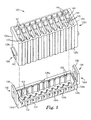
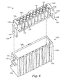
- Insulating housing 122 has a front exterior wall 124, laterally extending side exterior walls 126a, 126b, 126c, and 126d (hereafter collectively referred to as 126, unless otherwise indicated), and a plurality of laterally extending interior walls 128, collaboratively defining a plurality of cavities 142 configured to receive and position individual electrical cable terminations 108.
- Each electrical cable termination 108 is retained within its respective cavity 142 by a resilient latch 144 present in each cavity 142.
- a front edge 108b (as shown in Fig. 1 ) of electrical cable termination 108 engages a latch lead-in surface 148 and deflects latch 144 out of the path of electrical cable termination 108.
- latch 144 returns to its original (undeflected) position, and a latch hook member 150 engages a back edge 108c (as shown in Fig. 1 ) of electrical cable termination 108, thereby preventing electrical cable termination from being pulled out of carrier 106.
- Individual electrical cable terminations 108 can be removed from carrier 106 by simply deflecting latch 144 (as with a small tool or fingernail) to disengage latch hook member 150 from back edge 108c of electrical cable termination 108 while pulling gently on the associated electrical cable 110.
- the ability to remove and replace individual electrical cable terminations 108 is beneficial when replacing a damaged or defective electrical cable termination 108 of electrical cable 110, for example.
- carrier 106 further includes a wedge element 118 configured to secure the plurality of latch 144 and help retain the plurality of electrical cable terminations 108, as shown in Figure 4 .
- Wedge element 118 includes a plurality of wedges 146 configured to fit between latches 144 and side exterior wall 126a inside of cavities 142 of insulating housing 122. When properly installed, wedges 146 prevent latches 144 from deflecting out of the path of electrical cable terminations 108, thereby preventing electrical cable terminations 108 from being pulled out of carrier 106.
- electrical cable terminations 108 may be retained within carrier 106 by any suitable method/structure, including but not limited to snap fit, friction fit, press fit, mechanical clamping, and adhesive. Further, the method/structure used to retain electrical cable terminations 108 within carrier 106 may permit electrical cable terminations 108 to be removed individually, such as described above, the method/structure used to retain electrical cable terminations 108 within carrier 106 may permit electrical cable terminations 108 to be removed as a set, or the method/structure used to retain electrical cable terminations 108 within carrier 106 may permanently secure electrical cable terminations 108 within carrier 106. In other embodiments, cavities 142 of insulating housing 122 may be configured to receive more than one or all of the electrical cable terminations 108.
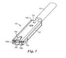
- Each interior wall 128 of insulating housing 122 has an aperture 130 configured to receive a second external electrical cable termination ground contact 158, described in further detail below and illustrated in Fig. 7 .
- Side exterior walls 126a and 126c include a plurality of apertures 132 that can be positioned in one or more of the side exterior walls 126. Each aperture 132 is configured to receive a first external electrical cable termination ground contact 156, described in further detail below and illustrated in Fig. 7 .
- apertures 132 can be positioned in side exterior walls 126a and 126c such that electrical cable terminations 108 can be positioned in insulating housing 122 either such that first external electrical cable termination ground contacts 156 are received in apertures 132 positioned in side exterior wall 126a, or such that first external electrical cable termination ground contacts 156 are received in apertures 132 positioned in side exterior wall 126a, or such that first external electrical cable termination ground contacts 156 are received in apertures 132 positioned in side exterior wall 126c.
- first and second insulating housing parts are designed such that second insulating housing part 122b can be assembled to first insulating housing part 122a either such that first external electrical cable termination ground contacts 156 of electrical cable terminations 108 are received in apertures 132 positioned in side exterior wall 126a, or such that first external electrical cable termination ground contacts 156 of electrical cable terminations 108 are received in apertures 132 positioned in side exterior wall 126c.
- This design enables electrical cables 110 to extend from electrical cable assembly 100 in two substantially different directions.
- Front exterior wall 124 has a plurality of contact pin insertion apertures 134 configured to receive contact pins 114 of header 104, illustrated in FIG. 1 . As shown in FIG.
- contact pin insertion apertures 134 preferably have a lead-in formed e.g. by chamfered edges to facilitate guidance and mating of contact pins 114 of header 104.
- front exterior wall 124 has a plurality of ground element insertion apertures 135 configured to receive ground elements 760 of header 704, described in further detail below and illustrated in FIG. 16 .
- Ground element insertion apertures 135 preferably have a lead-in formed e.g. by chamfered edges to facilitate guidance and mating of ground elements 760 of header 704.
- a significant advantage of an aspect of the present invention with respect to the prior art is that the various apertures described above enable arrangements of contact pins 114, ground contacts 156 and 158, and/or ground elements 760 that can provide an improved electrical performance of the electrical connector assembly.
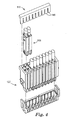
- side exterior walls 126b and 126d of insulating housing 122 include cooperative latch elements 136 configured to retain first insulating housing part 122a and second insulating housing part 122b in an assembled configuration.
- first insulating housing part 122a includes latch arms 138 that deflect to engage latch blocks 140 on second insulating housing part 122b. It is understood and intended that different and/or additional latch elements 136 may be provided as is suitable for the intended application.
- Electrical cable terminations that can be used in conjunction with carrier 106 can be constructed substantially similar to the shielded controlled impedance (SCI) connectors for a coaxial cable described in U.S. Pat. No. 5,184,965 .
- SCI shielded controlled impedance
- FIG. 7 an exemplary embodiment of an electrical cable termination that can be used in conjunction with carrier 106 is shown in FIG. 7 .
- Electrical cable termination 108 is coupled to electrical cable 110 through the use of solder opening 120.
- the electrical cable terminations are inserted into insulating housing 122 of carrier 106 (as best shown in FIG. 4 ) such that the front face 108a of electrical cable terminations 108 abuts interior surface 124a of front exterior wall 124 of insulating housing 122.
- Electrical cable termination 108 includes an electrically conductive housing 152 having mounted therein internal contacts 154.
- Each internal contact 154 can be designated as a signal/power contact, in which case it is electrically connected to a signal/power conductor of electrical cable 110 and electrically insulated from conductive housing 152.
- Each internal contact 154 can be designated as a ground contact, in which case it is electrically connected to a ground conductor (i.e. shield) of electrical cable 110 and/or to conductive housing 152.
- Internal contacts 152 are configured to make electrical contact with contact pins 114 of header 104. Internal contacts 152 lie along the longitudinal axis of electrical cable termination 108 and align with contact pin insertion apertures 134 of front exterior wall 124 of insulating housing 122.
- Electrical cable termination 108 further includes a first external electrical cable termination ground contact 156.
- First external electrical cable termination ground contact 156 extends from an external surface of conductive housing 152 and is configured to make electrical contact with a ground contact of a printed circuit board.
- the printed circuit board ground contact includes a plurality of ground pins 116, whereby first external electrical cable termination ground contacts 156 are configured to make electrical contact with corresponding ground pins 116 when header 104 and carrier 106 are in a mated configuration.
- the printed circuit board ground contact may include an electrically conductive strip or a plurality of ground pads, whereby first external electrical cable termination ground contacts 156 may be configured to make electrical contact with the electrically conductive strip or at least one of the plurality of ground pads when the header and carrier are in a mated configuration.
- Electrical cable termination 108 further includes a second external electrical cable termination ground contact 158 extending from an external surface of conductive housing 152.
- second external cable termination ground contacts 158 (as shown in Fig. 7 ) arc configured to make electrical contact with an adjacent electrical cable termination.
- a mating header may include a plurality of ground elements, whereby second external electrical cable termination ground contacts 158 may be configured to make electrical contact with one or more of the ground elements when the header and carrier are in a mated configuration.
- both first external electrical cable termination ground contacts 156 and second external electrical cable termination ground contacts 158 include resilient beams extending from conductive housing 152.
- first external electrical cable termination ground contacts 156 and/or second external electrical cable termination ground contacts 158 can take alternate forms from those illustrated, and may include, for example, a Hertzian bump extending from conductive housing 152.
- the type of electrical cable used in an aspect of the present invention can be a single wire cable (e.g. single coaxial or single twinaxial) or a multiple wire cable (e.g. multiple coaxial, multiple twinaxial, or twisted pair).
- Fig. 8 is a partial sectional side perspective view
- Fig. 9 is a cross-sectional view of an exemplary embodiment of an electrical cable 210 according to an aspect of the present invention.
- Electrical cable 210 includes conductor 212, dielectric sheath 214, metallic shield 216, and jacket 218.
- Dielectric sheath 214 is formed around conductor 212 so as to generally surround conductor 212.
- Metallic shield 216 is formed around dielectric sheath 214 so as to generally surround dielectric sheath 214.
- Jacket 218 envelops metallic shield 216 to form an outer protective casing for electrical cable 210.
- Conductor 212 may be made of a various conductive materials, including bare copper, tinned copper, silver plated copper, copper-covered steel, aluminum, or other suitable materials. Also, conductor 212 may be either a stranded or a solid element. In the case of a stranded element, conductor 212 is made of a plurality of electrically engaged conductive strands.
- Electrical cable 210 is used in high frequency signal applications, such as those greater than 100 MHz.
- the resistance of a conductor increases due to skin effect.
- Skin effect describes a condition where, due to magnetic fields produced by current flowing through the conductor, there is a concentration of current near the conductor surface.
- conductor 212 has a substantially oblong curvilinear cross-section.
- a substantially oblong curvilinear cross-section includes any elongated shape having rounded sides including, but not limited to, ovate, elliptical, capsule-shaped, and egg-shaped cross-sections.
- the substantially oblong curvilinear cross-section increases the surface area at the surface of conductor 212 over a conventional cylindrical conductor, the skin effect is minimized because more current flows along the larger surface. As a result, the signal attenuation characteristics of electrical cable 210 are improved since the overall resistance of conductor 212 is decreased.
- conductor 212 allows electrical cable 210 to be used with existing cable connectors.
- conductor 212 permits a larger thousand circular mils (MCM) gauge equivalent conductor to fit into the height space restrictions of existing micro-connectors.
- MCM circular mils
- the larger gauge conductor 212 also demonstrates better electrical performance (e.g., improved eye opening) due to improved rise time degradation characteristics.
- Dielectric sheath 214 is formed around conductor 212 to provide insulation between conductor 212 and metallic shield 216.
- the thickness of dielectric sheath 214 is adjustable to control the impedance of electrical cable 210, since the thickness of dielectric sheath 214 controls the spacing between conductor 212 and metallic shield 216.
- dielectric sheath 214 is extruded over conductor 212.
- dielectric sheath 214 is a tape or wrap made of a dielectric material.
- dielectric sheath 214 Exemplary materials that may be used for dielectric sheath 214 include polyvinyl chloride (PVC), fluoropolymers including perfluoroalkoxy (PFA), fluorinated ethylene propylene (FEP), and foamed fluorinated ethylene propylene (FFEP), and polyolefins such as polyethylene (PE), foamed polyethylene (FPE), polypropylene (PP), and polymethyl pentane.
- dielectric sheath 214 may comprise a dielectric tube and a solid core filament spacer to define an air core surrounding conductor 212, such as that shown and described in U.S. Pat. No. 6,849,799 , assigned to 3M Innovative Properties Company, St. Paul, Minn.
- Metallic shield 216 is formed around dielectric sheath 214 to shield conductor 212 from producing external electromagnetic interference (EMI). Metallic shield 216 also helps to prevent signal interference from electromagnetic and electrostatic fields outside of electrical cable 210. Furthermore, metallic shield 216 provides a continuous ground for electrical cable 210. In one embodiment, the interior surface of metallic shield 216 is an equal distance d from conductor 212 around the entire periphery of conductor 212, as shown in FIG. 9 . This results in even current distribution around the surface of conductor 212 (i.e., prevents current bunching), thus improving the signal attenuation characteristics of electrical cable 210. Metallic shield 216 may have a variety of configurations, including a metallic braid, a served shield, a metal foil, or combinations thereof.
- Jacket 218 is formed around metallic shield 216 and provides a protective coating for electrical cable 210 and support for the components of electrical cable 210. Jacket 218 also insulates the components of electrical cable 210 from external surroundings.
- outer surfaces 226 and 228 are substantially planar and parallel with surfaces 222 and 224 of conductor 212.
- Electrical cable 210 has a low profile in that the distance between surfaces 226 and 228 is less than the distance between the curved outer surfaces of electrical cable 210. This low profile allows electrical cable 210 to be used in applications having confined spaces or minimal amounts of extra space.
- Jacket 218 may be made of a flexible rubber material or a flexible plastic material, such as polyvinyl chloride (PVC), to permit installation of electrical cable 210 around obstructions and in tortuous passages.
- PVC polyvinyl chloride
- Other materials that may be used for jacket 218 include ethylene propylene diene (EPDM) elastomer, mica tape, neoprene, polyethylene, polypropylene, silicon, rubber, and fluoropolymer films available under the trade names TEFLON and TEFZEL from E.I. du Pont de Nemours and Company.
- FIG. 10 is a cross-sectional view of an electrical cable 310 including a drain wire 332 according to another embodiment of the present invention.
- Electrical cable 310 includes conductor 312, dielectric sheath 314, metallic shield 316, and jacket 318, similar to conductor 212, dielectric sheath 214, metallic shield 216, and jacket 218 as shown and described with regard to electrical cable 210 in Figs. 8 and 9 .
- Drain wire 332 is positioned outside of dielectric sheath 314, and metallic shield 316 surrounds and is in contact with drain wire 332 and dielectric sheath 314. In an alternative embodiment, drain wire 332 may be placed outside of and in contact with metallic shield 316.
- Jacket 318 is formed around metallic shield 316 and provides a protective coating for electrical cable 310 and a support structure for the elements of electrical cable 310.
- Drain wire 332 is in electrical contact with metallic shield 316. Drain wire 332 controls the impedance of electrical cable 310 by providing a method for electrical connection of metallic shield 316 to a connector. Drain wire 332 may be made of various conductive materials, including bare copper, tinned copper, silver plated copper, copper-covered steel, aluminum, or other suitable materials. Also, drain wire 332 may be either a stranded or a solid element. In the case of a stranded element, drain wire 332 is made of a plurality of electrically engaged conductive strands.
- Fig. 11 is a cross-sectional view of an electrical cable 410 according to another embodiment of the present invention.
- Electrical cable 410 includes conductors 452a and 452b, unitary dielectric sheath 454, metal foil 456, metallic wire shield 457, and jacket 458.
- Dielectric sheath 454 is formed around conductors 452a and 452b so as to generally surround conductors 452a and 452b.
- Metal foil 456 is formed around dielectric sheath 454 so as to generally surround dielectric sheath 454, and metallic wire shield 457 surrounds metal foil 456.
- Jacket 458 envelops metallic wire shield 457 to form an outer protective casing for electrical cable 410.
- Conductors 452a and 452b may be made of various conductive materials, including bare copper, tinned copper, silver plated copper, copper-covered steel, aluminum, or other suitable materials. Also, conductors 452a and 452b may be either a stranded or a solid element. In the case of a stranded element, each conductor is made of a plurality of electrically engaged conductive strands. In one embodiment, conductors 452a and 452b are positioned relative to each other such that major axes of the substantially oblong curvilinear cross-sections of conductors 452a and 452b are coplanar (as shown in Fig. 11 ).
- Electrical cable 410 is used in high frequency signal applications, such as those greater than 100 MHz. As described above, to minimize the skin effect, it is desirable to maximize the surface area of each conductor at the conductor surface. To increase the surface area over conventional cylindrical conductors, conductors 452a and 452b each have a substantially oblong curvilinear cross-section.
- a substantially oblong curvilinear cross-section includes any elongated shape having rounded sides including, but not limited to, ovate, elliptical, capsule-shaped, and egg-shaped cross-sections.
- the substantially oblong curvilinear cross-section increases the surface area at the surface of conductors 452a and 452b over conventional cylindrical conductors, the skin effect is minimized since more current flows along the larger surface. As a result, the signal attenuation characteristics of electrical cable 410 is improved since the overall resistance of conductors 452a and 452b is decreased.
- conductors 452a and 452b allow electrical cable 410 to be used with existing cable connectors.
- conductors 452a and 452b permit larger thousand circular mils (MCM) gauge equivalent conductors to fit into the height space restrictions of existing micro-connectors.
- MCM circular mils
- the larger gauge conductors 452a and 452b also demonstrate better electrical performance (e.g., improved eye opening) due to improved rise time degradation characteristics.
- Dielectric sheath 454 is formed around conductors 452a and 452b to provide insulation between conductors 452a and 452b and metal foil 456. In one embodiment, dielectric sheath 454 is extruded over conductors 452a and 452b. The thickness of dielectric sheath 454 is adjustable to control the impedance of electrical cable 410, since the thickness of dielectric sheath 454 controls the spacing between conductors 452a and 452b and metal foil 456. The orientation of and spacing between conductors 452a and 452b, which can also have an effect on the impedance of electrical cable 410, may also be controlled by the extrusion of dielectric sheath 454 over conductors 452a and 452b.
- dielectric sheath 454 Exemplary materials that may be used for dielectric sheath 454 include polyvinyl chloride (PVC), fluoropolymers including perfluoroalkoxy (PFA), fluorinated ethylene propylene (FEP), and foamed fluorinated ethylene propylene (FFEP), and polyolefins such as polyethylene (PE), foamed polyethylene (FPE), polypropylene (PP), and polymethyl pentane.
- dielectric sheath 454 may comprise a dielectric tube and a solid core filament spacer to define an air core surrounding conductors 452a and 452b, such as that shown and described in U.S. Pat. No. 6,849,799 .
- Metal foil 456 and metallic wire shield 457 are formed around dielectric sheath 454 to shield conductors 452a and 452b from producing external EMI. Metal foil 456 and metallic wire shield 457 also help to prevent signal interference from electromagnetic and electrostatic fields outside of electrical cable 410. The combination of metal foil 456 and metallic wire shield 457 provides excellent shielding properties. Furthermore, metal foil 456 and metallic wire shield 457 provide a continuous ground for electrical cable 410. Metal foil 456 may be comprised of a material such as copper and copper alloys. Metallic wire shield 457 may be comprised of a braided copper or copper alloys. Jacket 458 is formed around metallic wire shield 457 and provides a protective coating for electrical cable 410 and support for the components of electrical cable 410.
- Jacket 458 also insulates the components of electrical cable 410 from external surroundings.
- Electrical cable 410 has a low profile in that the distance D1 between the planar surfaces of electrical cable 410 is less than the distance D2 between the curved outer surfaces of electrical cable 410 (see FIG. 11 ). This low profile allows electrical cable 410 to be used in applications having confined spaces or minimal amounts of extra space.
- Jacket 458 may be made of a flexible rubber material or a flexible plastic material, such as polyvinyl chloride (PVC), to permit installation of electrical cable 410 around obstructions and in tortuous passages.
- PVC polyvinyl chloride
- jacket 458 Other materials that may be used for jacket 458 include ethylene propylene diene elastomer, mica tape, neoprene, polyethylene, polypropylene, silicon, rubber, and fluoropolymer films available under the trade names TEFLON and TEFZEL from E.I. du Pont de Nemours and Company.
- FIG. 12 is a cross-sectional view of electrical cable 510 according to another embodiment of the present invention including drain wire 562 and dielectric sheath 564 wrapped around conductors 552a and 552b.
- Electrical cable 510 includes metallic shield 556 and jacket 558, similar to metallic shield 456 and jacket 458 as shown and described with regard to electrical cable 410 in FIG. 11 .
- Drain wire 562 is positioned outside of dielectric sheath 564 between dielectric sheath 564 and metallic shield 556.
- Metallic shield 556 surrounds and is in contact with drain wire 562 and dielectric sheath 564. In an alternative embodiment, drain wire 562 may be placed outside of and in contact with metallic shield 556.
- Jacket 558 is formed around metallic shield 556 and provides a protective coating for electrical cable 510 and a support structure for the elements of electrical cable 510.
- Dielectric sheath 564 is taped or wrapped around conductors 552a and 552b to provide insulation between conductors 552a and 552b and metallic shield 556. Dielectric sheath 564 also controls the spacing between metal foil 556 and conductors 552a and 552b, the spacing between conductors 552a and 552b, and the orientation of conductors 552a and 552b. Because all of these parameters have an effect on the impedance of electrical cable 510, the impedance can be controlled by adjusting the thickness of dielectric sheath 564 and the orientation of conductors 552a and 552b held by dielectric sheath 564.
- dielectric sheath 564 may be extruded over conductors 552a and 552b, similar to dielectric sheath 454 in Fig. 11 .
- Exemplary materials that may be used for dielectric sheath 564 include polyvinyl chloride (PVC), fluoropolymers including perfluoroalkoxy (PFA), fluorinated ethylene propylene (FEP), and foamed fluorinated ethylene propylene (FFEP), and polyolefins such as polyethylene (PE), foamed polyethylene (FPE), polypropylene (PP), and polymethyl pentane.
- PVC polyvinyl chloride
- FEP fluorinated ethylene propylene
- FFEP foamed fluorinated ethylene propylene
- PE polyethylene
- FPE foamed polyethylene
- PP polypropylene
- polymethyl pentane polymethyl pentane
- dielectric sheath 564 may comprise a dielectric tube and a solid core filament spacer to define an air core surrounding conductors 552a and 552b, such as that shown and described in the previously incorporated U.S. Patent No. 6,849,799 .
- Electrical connector assembly 600 includes a printed circuit board 602, a header 604 coupled to printed circuit board 602, and carrier 106 retaining terminations 108 of individual electrical cables 110.
- Carrier 106 is configured to mate with header 604 to provide an interconnection between printed circuit board 602 and electrical cables 110.
- Carrier 106, terminations 108, and electrical cables 110 were shown and described with regard to electrical connector assembly 100.
- header 604 includes an insulative housing 612 containing a plurality of contact pins 614 arranged for mating with the internal contacts of electrical cable terminations 108 in carrier 106.
- Contact pins 614 of header 604 are connected to printed circuit board 602 as is known in the art.
- Contact pins 614 are configured for electrical connection to one or more of a plurality of electrical traces (not shown) of printed circuit board 602.
- header 604 is shown and described herein as a through-hole pin header, header 604 may also be a surface-mount pin header or any other suitable type of header known in the art.
- Contact pins 614 may be connected to printed circuit board 602 by soldering, press-fit, or any other suitable approach. In the embodiment of Fig.
- header 604 is secured to printed circuit board 602 only by the connection between contact pins 614 and printed circuit board 602.
- header 604 may include additional structure(s) for securing header 604 to printed circuit board 602, such as mounting posts on insulative housing 612 configured for insertion into holes in printed circuit board 602 (not shown). The mounting posts may be retained in the holes in the printed circuit board 602 by press-fit, adhesive, or other suitable approach.
- header 604 is a right angle pin header, whereby contact pins 614 have a substantially right angle configuration, enabling an insertion of carrier 106 in a direction substantially parallel to printed circuit board 602.
- Printed circuit board 602 is substantially conventional in design except for the addition of a printed circuit board ground contact.
- the printed circuit board ground contact includes an electrically conductive strip 616.
- Each of the plurality of electrical cable terminations 108 is preferably configured to make electrical contact with electrically conductive strip 616 when header 604 and carrier 106 are in a mated configuration.
- Electrically conductive strip 616 is connected to printed circuit board 602 as is known in the art.
- electrically conductive strip 616 may as be connected to printed circuit board 602 by soldering, press-fit, or any other suitable approach.
- electrically conductive strip 616 may be included in the printed circuit board artwork and thereby electrochemically deposited onto printed circuit board 602.
- electrically conductive strip 616 extends continuously along the length of header 604, so that first external electrical cable termination ground contact 156 of each of the electrical cable terminations 108 a connected to a common ground. In another embodiment, electrically conductive strip 616 extends along less than all of the first external electrical cable termination ground contact 156. In yet another embodiment, electrically conductive strip 616 is separated into two or more separate segments, such that only selected ones of the first external electrical cable termination ground contacts 156 are connected to electrically conductive strip 616. In an alternative embodiment, the printed circuit board ground contact includes a plurality of ground pads.
- Each of the plurality of electrical cable terminations 108 is configured to make electrical contact with at least one of the plurality of ground pads when header 604 and carrier 106 are in a mated configuration.
- the ground pads are connected to printed circuit board 602 as is known in the art.
- the ground pads may be included in the printed circuit board artwork and thereby electrochemically deposited onto printed circuit board 602.
- Header 604 and electrical cable terminations 108 may be configured such that each of the plurality of electrical cable terminations 108 makes electrical contact with one or more of contact pins 614 of header 604 and a printed circuit board ground contact when header 604 and carrier 106 are in a mated configuration.
- header 604 and electrical cable terminations 108 are configured such that each of the plurality of electrical cable terminations 108 makes electrical contact with two of the contact pins 614, illustrated in Fig. 14 as 614a and 614b, of header 604 and electrically conductive strip 616 connected to printed circuit board 602, when header 604 and carrier 106 are in a mated configuration.
- a ground-signal-ground (GSG) configuration can be formed for improved impedance control through the interconnect by designating contact pin 614a as a ground contact, contact pin 614b as a signal contact, and electrically conductive strip 616 as a ground contact. It is understood and intended that any of contact pins 614 and electrically conductive strip 616 can be designated as signal, ground, or power contacts as is suitable for the intended application. Further, it is understood and intended that any of contact pins 614 can be eliminated from the array of pins and that portions of electrically conductive strip 616 can be eliminated as is suitable for the intended application.
- first external electrical cable termination ground contacts 156 (as shown in Fig. 7 ) of electrical cable terminations 108 are configured to make electrical contact with electrically conductive strip 616 when header 604 and carrier 106 are in a mated configuration.
- Second external cable termination ground contacts 158 (as shown in Fig. 7 ) are configured to make electrical contact with an adjacent electrical cable termination.
- Electrical connector assembly 700 includes a printed circuit board 702, a header 704 coupled to printed circuit board 702, and carrier 106 retaining terminations 108 of individual electrical cables 110.
- Carrier 106 is configured to mate with header 704 to provide an interconnection between printed circuit board 702 and electrical cables 110.
- Carrier 106, terminations 108, and electrical cables 110 were shown and described above with regard to electrical connector assembly 100.
- header 704 and carrier 106 include cooperative latch elements 780 configured to retain header 704 and carrier 106 in a mated configuration.
- header 704 includes latch arms 782 that rotate to engage latch block 784 on opposing side exterior walls 126b and 126d of insulating housing 122 of carrier 106.
- Latch arms 782 may be configured to automatically rotate into engagement with latch block 784 as carrier 106 is mated with header 704, or may alternatively be configured to require manual latching by the user.
- Different and/or additional latch elements 780 may be provided as is suitable for the intended application.
- header 704 includes an insulative housing 712 containing a plurality of contact pins 714 arranged for mating with the internal contacts of electrical cable terminations 108 in carrier 106.
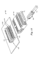
- insulative housing 712 contains a plurality of ground elements 760 arranged for mating with the second external electrical cable termination ground contacts 158 of electrical cable termination 108 in carrier 106, as best shown in Fig. 17 .
- Ground elements 760 may include ground blades, ground pins, and/or any other electrical contact types suitable to facilitate electrical grounding and/or electrical shielding functions.
- Contact pins 714 and ground elements 760 of header 704 are connected to printed circuit board 702 as is known in the art.
- Contact pins 714 and ground elements 760 are configured for electrical connection to one or more of a plurality of electrical traces (not shown) of printed circuit board 702.
- header 704 may also be a surface-mount pin header or any other suitable type of header known in the art, including combinations of a through-hole pin header and a surface-mount pin header.
- header 704 is a surface-mount pin header, whereby contact pins 714 have a surface-mount configuration, but whereby ground elements 760 have a through-hole configuration.
- Contact pins 714 and ground elements 760 may be connected to printed circuit board 702 by soldering, press-fit, or any other suitable approach. In the embodiment of Fig.
- header 704 is secured to printed circuit board 702 only by the connection between contact pins 714 and ground elements 760 and printed circuit board 702.
- header 704 may include additional structure(s) for securing header 704 to printed circuit board 702, such as mounting posts on insulative housing 712 configured for insertion into holes in printed circuit board 702 (not shown). The mounting posts may be retained in the holes in the printed circuit board 702 by press-fit, adhesive, or other suitable approach.
- header 704 is a straight or vertical pin header, whereby contact pins 714 and ground elements 760 have a substantially straight or vertical configuration, enabling an insertion of carrier 106 in a direction substantially perpendicular to printed circuit board 702.
- Header 704 and electrical cable terminations 108 may be configured such that each of the plurality of electrical cable terminations 108 makes electrical contact with one or more of contact pins 714 of header 704, ground elements 760 of header 704, and a printed circuit board ground contact when header 704 and carrier 106 are in a mated configuration.
- header 704 and electrical cable terminations 108 are configured such that each of the plurality of electrical cable terminations 108 makes electrical contact with two of the contact pins 714 of header 704, one of the ground elements 760 of header 704, and a printed circuit board ground contact (not shown) when header 704 and carrier 106 are in a mated configuration.
- any of contact pins 714, ground elements 760, and the printed circuit board ground contact can be designated as signal, ground, or power contacts as is suitable for the intended application. Further, it is understood and intended that any of contact pins 714 and/or ground elements 760 can be eliminated from the array of pins/elements as is suitable for the intended application.
- first external electrical cable termination ground contacts 156 (as shown in Fig. 7 ) of electrical cable terminations 108 are configured to make electrical contact with a printed circuit board ground contact (not shown) when header 704 and carrier 106 are in a mated configuration.
- Second external cable termination ground contacts 158 (as shown in Fig. 7 ) are configured to make electrical contact with corresponding ground elements 760 when the header and carrier are in a mated configuration.
- the various components of the electrical connector assembly and elements thereof are formed of any suitable material.
- the materials are selected depending upon the intended application and may include both polymers and metals.
- insulating housing 122 of carrier 106 and insulative housing 112 of header 104 are formed of polymeric materials by methods such as injection molding, extrusion, casting, machining, and the like, while the electrically conductive components are formed of metal by methods such as molding, casting, stamping, machining the like. Material selection will depend upon factors including, but not limited to, chemical exposure conditions, environmental exposure conditions including temperature and humidity conditions, flame-retardancy requirements, material strength, and rigidity, to name a few.
Description
- The present invention relates generally to interconnections made between a printed circuit board and one or more electrical cables carrying signals to and from the printed circuit board.
- The interconnection of printed circuit boards to other circuit boards, cables, or other electronic devices is well known in the art. Such interconnections typically have not been difficult to form, especially when the circuit switching speeds (also referred to as signal transition times) have been slow when compared to the length of time required for a signal to propagate through a conductor in the interconnect or on the printed circuit board. However, as circuit switching speeds continue to increase with modem integrated circuits and related computer technology, the design and fabrication of satisfactory interconnects has grown more difficult.
- Specifically, there is a continued and growing need to design and fabricate printed circuit boards and their accompanying interconnects with closely controlled electrical characteristics to achieve satisfactory control over the integrity of the signal as it travels through the interconnect to and from the printed circuit board. The extent to which electrical characteristics (such as impedance) of the interconnect must be controlled depends heavily upon the switching speed of the circuit. That is, the faster the circuit switching speed, the greater the importance of providing an accurately controlled impedance within the interconnect.
- Connector systems developed for high-speed board-to-board and board-to-cable interconnect applications are replete in the art. In general, an optimum printed circuit board interconnect design minimizes the length of marginally controlled signal line characteristic impedance by minimizing the physical spacing between the printed circuit board and the connector. Also, connector designs which involve relatively large pin and socket connectors with multiple pins devoted to power and ground contacts provide only marginally acceptable performance for high speed printed circuit boards.
-
US 2007141871 discloses an electrical connector assembly for transmitting high speed electrical signals, that includes a header and a carrier. The header has a plurality of signal pins, a plurality of ground pins, and a supplemental ground contact. The carrier is configured to mate with the header. A plurality of electrical cable terminations are retained by the carrier, and the header and cable terminations are configured such that each of the plurality of electrical cable terminations makes electrical contact with one or more of the signal pins, ground pins, and supplemental ground contact when the header and carrier are in a mated configuration. -
WO 2005109578 discloses an electrical connector that includes an insulative carrier having therein at least one cable connector. The carrier is configured to engage a header having a plurality of signal pins and a plurality of shield blades extending therefrom. Each cable connector terminates a corresponding cable and includes a conductive outer housing having an insulative inner housing. The inner housing holds first and second conductive terminals in electrical isolation from each other and the outer housing. The inner housing is configured for receiving a shield blade between the first and second terminals. The outer housing includes a first contact for electrically coupling with the shield blade received between the first and second terminals. - Unfortunately, currently available high speed interconnect solutions for board-to-cable applications are typically complex, requiring extremely accurate component designs which are very sensitive to even small manufacturing variations and which, as a result, are expensive and difficult to manufacture. Even then, the performance of the available board-to-cable interconnect systems is becoming only marginally acceptable as switching speeds continue to increase. What is needed is a printed circuit board-to-cable interconnect system that provides the necessary impedance control for high speed integrated circuits while still being inexpensive and easy to manufacture.
- In one aspect, the present invention provides a carrier for use with an electrical connector assembly. The carrier includes an insulating housing having a front exterior wall on which a plurality of contact pin insertion apertures is disposed. The insulating housing further includes side exterior walls laterally extending from the front exterior wall. A plurality of first apertures is disposed on at least one of the side exterior walls. Each first aperture is configured to receive a first external electrical cable termination ground contact. The insulating housing further includes a plurality of interior walls laterally extending from the front exterior wall. Each of the plurality of interior walls includes a second aperture configured to receive a second external electrical cable termination ground contact. Optionally, the insulating housing may include a first housing part and a second housing part.
- In another aspect, the present invention provides an electrical connector assembly including a printed circuit board having a printed circuit board ground contact, a header coupled to the printed circuit board and comprising a plurality of contact pins, a carrier, and a plurality of electrical cable terminations retained by the carrier. The carrier includes an insulating housing having a front exterior wall on which a plurality of contact pin insertion apertures is disposed. The insulating housing further includes side exterior walls laterally extending from the front exterior wall. A plurality of first apertures is disposed on at least one of the side exterior walls. Each first aperture is configured to receive a first external electrical cable termination ground contact. The insulating housing further includes a plurality of interior walls laterally extending from the front exterior wall. Each of the plurality of interior walls includes a second aperture configured to receive a second external electrical cable termination ground contact. The header and electrical cable terminations are configured such that each of the plurality of electrical cable terminations makes electrical contact with one or more of the contact pins and printed circuit board ground contact when the header and carrier are in a mated configuration.
- In another aspect, the present invention provides an electrical connector assembly including a printed circuit board having a printed circuit board ground contact, a header coupled to the printed circuit board and comprising a plurality of contact pins and a plurality of ground elements, a carrier, and a plurality of electrical cable terminations retained by the carrier. The carrier includes an insulating housing having a front exterior wall on which a plurality of contact pin insertion apertures and a plurality of ground element insertion apertures are disposed. The insulating housing further includes side exterior walls laterally extending from the front exterior wall. A plurality of first apertures is disposed on at least one of the side exterior walls. Each first aperture is configured to receive a first external electrical cable termination ground contact. The insulating housing further includes a plurality of interior walls laterally extending from the front exterior wall. Each of the plurality of interior walls includes a second aperture configured to receive a second external electrical cable termination ground contact. The header and electrical cable terminations are configured such that each of the plurality of electrical cable terminations makes electrical contact with one or more of the contact pins, ground elements, and printed circuit board ground contact when the header and carrier are in a mated configuration.
- The above summary of the present invention is not intended to describe each disclosed embodiment or every implementation of the present invention. The Figures and detailed description that follow below more particularly exemplify illustrative embodiments.
-
-
Fig. 1 is a perspective view of an exemplary embodiment of an electrical connector assembly according to an aspect of the present invention. -
Fig. 2 is a side view of the electrical connector assembly ofFig. 1 showing the header and carrier of the electrical connector assembly in an unmated configuration. -
Fig. 3 is a side view of the electrical connector assembly ofFig. 1 showing the header and carrier of the electrical connector assembly in a mated configuration. -
Fig. 4 is a perspective view of an exemplary embodiment of a carrier and a plurality of electrical cable terminations according to an aspect of the present invention. -
Fig. 5 is a top perspective view of an exemplary embodiment of a carrier according to an aspect of the present invention. -
Fig. 6 is a bottom perspective view of the carrier ofFig. 5 . -
Fig. 7 is a perspective view of an exemplary embodiment of an electrical cable termination that can be used in the electrical connector assembly ofFig. 1 . -
Fig. 8 is a partial sectional side perspective view of an electrical cable according to an aspect of the present invention. -
Fig. 9 is a cross-sectional view of the cable shown inFig. 8 , as taken along lines 9-9 inFig. 8 . -
Fig. 10 is a cross-sectional view of another exemplary embodiment of an electrical cable according to an aspect of the present invention. -
Fig. 11 is a cross-sectional view of another exemplary embodiment of an electrical cable according to an aspect of the present invention. -
Fig. 12 is a cross-sectional view of another exemplary embodiment of an electrical cable according to an aspect of the present invention. -
Fig. 13 is a perspective view of another exemplary embodiment of an electrical connector assembly according to an aspect of the present invention. -
Fig. 14 is a side view of the electrical connector assembly ofFig. 13 showing the header and carrier of the electrical connector assembly in an unmated configuration. -
Fig. 15 is a side view of the electrical connector assembly ofFig. 13 showing the header and carrier of the electrical connector assembly in a mated configuration. -
Fig. 16 is a perspective view of another exemplary embodiment of an electrical connector assembly according to an aspect of the present invention. -
Fig. 17 is a perspective cross-sectional view of the electrical connector assembly ofFig. 16 . -
Fig. 18 is a perspective view of the electrical connector assembly ofFig. 16 showing the header and carrier of the electrical connector assembly in a mated configuration. - In the following detailed description of the preferred embodiments, reference is made to the accompanying drawings that form a part hereof. The accompanying drawings show, by way of illustration, specific embodiments in which the invention may be practiced. It is to be understood that other embodiments may be utilized, and structural or logical changes may be made without departing from the scope of the present invention. The following detailed description, therefore, is not to be taken in a limiting sense, and the scope of the invention is defined by the appended claims and their equivalents.
-
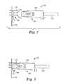
Figs. 1-3 illustrate an exemplary embodiment of an electrical connector assembly according to an aspect of the present invention.Electrical connector assembly 100 includes a printedcircuit board 102, aheader 104 coupled to printedcircuit board 102, and acarrier 106 retainingterminations 108 of individualelectrical cables 110.Carrier 106 is configured to mate withheader 104 to provide an interconnection between printedcircuit board 102 andelectrical cables 110. - For purpose of clarity, aspects of the invention are described and illustrated herein as used with twinaxial cables and twinaxial cable terminations. However, such illustration is exemplary only, and it is understood and intended that other types of electrical cables and their associated electrical cable terminations can be used, including but not limited to coaxial cables and other cable configurations with signal and ground elements. It is further understood and intended that different types and configurations of electrical cables and electrical cable terminations may be used simultaneously with electrical connector assemblies according to aspects of the present invention. For example, a portion of electrical cable terminations retained by a carrier may be twinaxial cable terminations, while another portion of electrical cable terminations retained by a carrier may be coaxial cable (or other) terminations.
- Referring to
Fig. 1 ,header 104 includes aninsulative housing 112 containing a plurality of contact pins 114 arranged for mating with the internal contacts ofelectrical cable terminations 108 incarrier 106. Contact pins 114 ofheader 104 are connected to printedcircuit board 102 as is known in the art. Contact pins 114 are configured for electrical connection to one or more of a plurality of electrical traces (not shown) of printedcircuit board 102. Althoughheader 104 is shown and described herein as a through-hole pin header,header 104 may also be a surface-mount pin header or any other suitable type of header known in the art. Contact pins 114 may be connected to printedcircuit board 102 by soldering, press-fit, or any other suitable approach. In the embodiment ofFig. 1 ,header 104 is secured to printedcircuit board 102 only by the connection between contact pins 1 14 and printedcircuit board 102. Alternatively,header 104 may include additional structure(s) for securingheader 104 to printedcircuit board 102, such as mounting posts oninsulative housing 112 configured for insertion into holes in printed circuit board 102 (not shown). The mounting posts may be retained in the holes in the printedcircuit board 102 by press-fit, adhesive, or other suitable approach. In the embodiment ofFig. 1 ,header 104 is a straight or vertical pin header, whereby contact pins 114 have a substantially straight or vertical configuration, enabling an insertion ofcarrier 106 in a direction substantially perpendicular to printedcircuit board 102. An exemplary header that can be used in an electrical connector assembly according to an aspect of the present invention is shown and described inU.S. Provisional Application No. 60/886229 , incorporated by reference herein in its entirety. - Printed
circuit board 102 is substantially conventional in design except for the addition of a printed circuit board ground contact. In the exemplary embodiment ofFig. 1 , the printed circuit board ground contact includes a plurality of ground pins 116. Each of the plurality ofelectrical cable terminations 108 is configured to make electrical contact with one of the plurality of ground pins 116 whenheader 104 andcarrier 106 are in a mated configuration. Ground pins 116 are connected to printedcircuit board 102 as is known in the art. Ground pins 116 are configured for electrical connection to one or more of a plurality of electrical traces (not shown) of printedcircuit board 102. Although ground pins 116 are shown and described herein as through-hole pins, ground pins 116 may also be surface-mount pins or any other suitable type of contact pins known in the art. Contact pins 116 may be connected to printedcircuit board 102 by soldering, press-fit, or any other suitable approach. -
Header 104 andelectrical cable terminations 108 may be configured such that each of the plurality ofelectrical cable terminations 108 makes electrical contact with one or more of contact pins 114 ofheader 104 and a printed circuit board ground contact whenheader 104 andcarrier 106 are in a mated configuration. In the exemplary embodiment ofFigs. 1-3 , as best seen in the side views ofFigs. 2 and 3 ,header 104 andelectrical cable terminations 108 are configured such that each of the plurality ofelectrical cable terminations 108 makes electrical contact with two of the contact pins 114, illustrated inFig. 2 as 114a and 114b, ofheader 104 and one of the ground pins 116 connected to printedcircuit board 102, whenheader 104 andcarrier 106 are in a mated configuration. In one aspect, a ground-signal-ground (GSG) configuration can be formed for improved impedance control through the interconnect by designatingcontact pin 114a as a ground contact,contact pin 114b as a signal contact, andground pin 116 as a ground contact. It is understood and intended that any of contact pins 114 and ground pins 116 can be designated as signal, ground, or power contacts as is suitable for the intended application. Further, it is understood and intended that any of contact pins 114 and ground pins 116 can be eliminated from the array of pins as is suitable for the intended application. -
Figs. 4-6 show different perspective views of a carrier according to an aspect of the present invention. As best seen inFig. 4 ,carrier 106 ofelectrical connector assembly 100 is configured to retain a plurality ofelectrical cable terminations 108 and includes an insulatinghousing 122. - Referring to
Figs. 5 and6 , insulatinghousing 122 includes a first insulatinghousing part 122a and a second insulatinghousing part 122b. In an alternative aspect, insulatinghousing parts housing 122. Insulatinghousing 122 has a frontexterior wall 124, laterally extending sideexterior walls interior walls 128, collaboratively defining a plurality ofcavities 142 configured to receive and position individualelectrical cable terminations 108. - Each
electrical cable termination 108 is retained within itsrespective cavity 142 by aresilient latch 144 present in eachcavity 142. As anelectrical cable termination 108 is inserted into itsrespective cavity 142, afront edge 108b (as shown inFig. 1 ) ofelectrical cable termination 108 engages a latch lead-insurface 148 and deflectslatch 144 out of the path ofelectrical cable termination 108. Aselectrical cable termination 108 is fully inserted, latch 144 returns to its original (undeflected) position, and alatch hook member 150 engages aback edge 108c (as shown inFig. 1 ) ofelectrical cable termination 108, thereby preventing electrical cable termination from being pulled out ofcarrier 106. Individualelectrical cable terminations 108 can be removed fromcarrier 106 by simply deflecting latch 144 (as with a small tool or fingernail) to disengagelatch hook member 150 fromback edge 108c ofelectrical cable termination 108 while pulling gently on the associatedelectrical cable 110. The ability to remove and replace individualelectrical cable terminations 108 is beneficial when replacing a damaged or defectiveelectrical cable termination 108 ofelectrical cable 110, for example. - In one embodiment,
carrier 106 further includes awedge element 118 configured to secure the plurality oflatch 144 and help retain the plurality ofelectrical cable terminations 108, as shown inFigure 4 .Wedge element 118 includes a plurality ofwedges 146 configured to fit betweenlatches 144 and sideexterior wall 126a inside ofcavities 142 of insulatinghousing 122. When properly installed,wedges 146 preventlatches 144 from deflecting out of the path ofelectrical cable terminations 108, thereby preventingelectrical cable terminations 108 from being pulled out ofcarrier 106. - In other embodiments,
electrical cable terminations 108 may be retained withincarrier 106 by any suitable method/structure, including but not limited to snap fit, friction fit, press fit, mechanical clamping, and adhesive. Further, the method/structure used to retainelectrical cable terminations 108 withincarrier 106 may permitelectrical cable terminations 108 to be removed individually, such as described above, the method/structure used to retainelectrical cable terminations 108 withincarrier 106 may permitelectrical cable terminations 108 to be removed as a set, or the method/structure used to retainelectrical cable terminations 108 withincarrier 106 may permanently secureelectrical cable terminations 108 withincarrier 106. In other embodiments,cavities 142 of insulatinghousing 122 may be configured to receive more than one or all of theelectrical cable terminations 108. - Each
interior wall 128 of insulatinghousing 122 has anaperture 130 configured to receive a second external electrical cabletermination ground contact 158, described in further detail below and illustrated inFig. 7 .Side exterior walls apertures 132 that can be positioned in one or more of the side exterior walls 126. Eachaperture 132 is configured to receive a first external electrical cabletermination ground contact 156, described in further detail below and illustrated inFig. 7 . In one embodiment,apertures 132 can be positioned in sideexterior walls electrical cable terminations 108 can be positioned in insulatinghousing 122 either such that first external electrical cabletermination ground contacts 156 are received inapertures 132 positioned inside exterior wall 126a, or such that first external electrical cabletermination ground contacts 156 are received inapertures 132 positioned inside exterior wall 126a, or such that first external electrical cabletermination ground contacts 156 are received inapertures 132 positioned in sideexterior wall 126c. In the illustrated embodiment of insulatinghousing 122, first and second insulating housing parts are designed such that second insulatinghousing part 122b can be assembled to first insulatinghousing part 122a either such that first external electrical cabletermination ground contacts 156 ofelectrical cable terminations 108 are received inapertures 132 positioned inside exterior wall 126a, or such that first external electrical cabletermination ground contacts 156 ofelectrical cable terminations 108 are received inapertures 132 positioned in sideexterior wall 126c. This design enableselectrical cables 110 to extend fromelectrical cable assembly 100 in two substantially different directions.Front exterior wall 124 has a plurality of contactpin insertion apertures 134 configured to receivecontact pins 114 ofheader 104, illustrated inFIG. 1 . As shown inFIG. 6 , contactpin insertion apertures 134 preferably have a lead-in formed e.g. by chamfered edges to facilitate guidance and mating of contact pins 114 ofheader 104. Optionally, frontexterior wall 124 has a plurality of groundelement insertion apertures 135 configured to receiveground elements 760 ofheader 704, described in further detail below and illustrated inFIG. 16 . Groundelement insertion apertures 135 preferably have a lead-in formed e.g. by chamfered edges to facilitate guidance and mating ofground elements 760 ofheader 704. A significant advantage of an aspect of the present invention with respect to the prior art is that the various apertures described above enable arrangements of contact pins 114,ground contacts ground elements 760 that can provide an improved electrical performance of the electrical connector assembly. In one embodiment, sideexterior walls housing 122 includecooperative latch elements 136 configured to retain first insulatinghousing part 122a and second insulatinghousing part 122b in an assembled configuration. In the embodiment illustrated inFIGS. 5 and6 , first insulatinghousing part 122a includes latcharms 138 that deflect to engage latch blocks 140 on second insulatinghousing part 122b. It is understood and intended that different and/oradditional latch elements 136 may be provided as is suitable for the intended application. - Electrical cable terminations that can be used in conjunction with
carrier 106 can be constructed substantially similar to the shielded controlled impedance (SCI) connectors for a coaxial cable described inU.S. Pat. No. 5,184,965 . - In particular, an exemplary embodiment of an electrical cable termination that can be used in conjunction with
carrier 106 is shown inFIG. 7 .Electrical cable termination 108 is coupled toelectrical cable 110 through the use ofsolder opening 120. For use in conjunction withcarrier 106, the electrical cable terminations are inserted into insulatinghousing 122 of carrier 106 (as best shown inFIG. 4 ) such that thefront face 108a ofelectrical cable terminations 108 abutsinterior surface 124a of frontexterior wall 124 of insulatinghousing 122.Electrical cable termination 108 includes an electricallyconductive housing 152 having mounted thereininternal contacts 154. Eachinternal contact 154 can be designated as a signal/power contact, in which case it is electrically connected to a signal/power conductor ofelectrical cable 110 and electrically insulated fromconductive housing 152. Eachinternal contact 154 can be designated as a ground contact, in which case it is electrically connected to a ground conductor (i.e. shield) ofelectrical cable 110 and/or toconductive housing 152.Internal contacts 152 are configured to make electrical contact withcontact pins 114 ofheader 104.Internal contacts 152 lie along the longitudinal axis ofelectrical cable termination 108 and align with contactpin insertion apertures 134 of frontexterior wall 124 of insulatinghousing 122. -
Electrical cable termination 108 further includes a first external electrical cabletermination ground contact 156. First external electrical cabletermination ground contact 156 extends from an external surface ofconductive housing 152 and is configured to make electrical contact with a ground contact of a printed circuit board. In the exemplary embodiment of an electrical connector assembly shown inFIG. 1 , the printed circuit board ground contact includes a plurality of ground pins 116, whereby first external electrical cabletermination ground contacts 156 are configured to make electrical contact with corresponding ground pins 116 whenheader 104 andcarrier 106 are in a mated configuration. In other embodiments, the printed circuit board ground contact may include an electrically conductive strip or a plurality of ground pads, whereby first external electrical cabletermination ground contacts 156 may be configured to make electrical contact with the electrically conductive strip or at least one of the plurality of ground pads when the header and carrier are in a mated configuration. -
Electrical cable termination 108 further includes a second external electrical cabletermination ground contact 158 extending from an external surface ofconductive housing 152. In the exemplary embodiment of an electrical connector assembly shown inFIG. 1 , second external cable termination ground contacts 158 (as shown inFig. 7 ) arc configured to make electrical contact with an adjacent electrical cable termination. In other embodiments, a mating header may include a plurality of ground elements, whereby second external electrical cabletermination ground contacts 158 may be configured to make electrical contact with one or more of the ground elements when the header and carrier are in a mated configuration. - In the illustrated embodiments, both first external electrical cable
termination ground contacts 156 and second external electrical cabletermination ground contacts 158 include resilient beams extending fromconductive housing 152. In other embodiments, first external electrical cabletermination ground contacts 156 and/or second external electrical cabletermination ground contacts 158 can take alternate forms from those illustrated, and may include, for example, a Hertzian bump extending fromconductive housing 152. - The type of electrical cable used in an aspect of the present invention can be a single wire cable (e.g. single coaxial or single twinaxial) or a multiple wire cable (e.g. multiple coaxial, multiple twinaxial, or twisted pair).
Fig. 8 is a partial sectional side perspective view andFig. 9 is a cross-sectional view of an exemplary embodiment of anelectrical cable 210 according to an aspect of the present invention.Electrical cable 210 includesconductor 212,dielectric sheath 214,metallic shield 216, andjacket 218.Dielectric sheath 214 is formed aroundconductor 212 so as to generally surroundconductor 212.Metallic shield 216 is formed arounddielectric sheath 214 so as to generally surrounddielectric sheath 214.Jacket 218 envelopsmetallic shield 216 to form an outer protective casing forelectrical cable 210. -
Conductor 212 may be made of a various conductive materials, including bare copper, tinned copper, silver plated copper, copper-covered steel, aluminum, or other suitable materials. Also,conductor 212 may be either a stranded or a solid element. In the case of a stranded element,conductor 212 is made of a plurality of electrically engaged conductive strands. -
Electrical cable 210 is used in high frequency signal applications, such as those greater than 100 MHz. As described above, as signal frequency increases, the resistance of a conductor increases due to skin effect. Skin effect describes a condition where, due to magnetic fields produced by current flowing through the conductor, there is a concentration of current near the conductor surface. To maximize the surface area at the conductor surface,conductor 212 has a substantially oblong curvilinear cross-section. A substantially oblong curvilinear cross-section includes any elongated shape having rounded sides including, but not limited to, ovate, elliptical, capsule-shaped, and egg-shaped cross-sections. Because the substantially oblong curvilinear cross-section increases the surface area at the surface ofconductor 212 over a conventional cylindrical conductor, the skin effect is minimized because more current flows along the larger surface. As a result, the signal attenuation characteristics ofelectrical cable 210 are improved since the overall resistance ofconductor 212 is decreased. - In addition, in conventional approaches to improving the signal attenuation characteristics of electrical cables, larger cylindrical conductor diameters are used to compensate for the increase in resistance at higher frequencies. Larger inner conductor diameter sizes typically require larger volumes of dielectric surrounding the conductor to maintain desired cable impedance. This increases the overall size of the cable and prevents the cable from being used with standard micro-connectors used in high frequency systems. The substantially oblong curvilinear cross-section of
conductor 212 allowselectrical cable 210 to be used with existing cable connectors. In particular,conductor 212 permits a larger thousand circular mils (MCM) gauge equivalent conductor to fit into the height space restrictions of existing micro-connectors. Thelarger gauge conductor 212 also demonstrates better electrical performance (e.g., improved eye opening) due to improved rise time degradation characteristics. -
Dielectric sheath 214 is formed aroundconductor 212 to provide insulation betweenconductor 212 andmetallic shield 216. The thickness ofdielectric sheath 214 is adjustable to control the impedance ofelectrical cable 210, since the thickness ofdielectric sheath 214 controls the spacing betweenconductor 212 andmetallic shield 216. In one embodiment,dielectric sheath 214 is extruded overconductor 212. In another embodiment,dielectric sheath 214 is a tape or wrap made of a dielectric material. Exemplary materials that may be used fordielectric sheath 214 include polyvinyl chloride (PVC), fluoropolymers including perfluoroalkoxy (PFA), fluorinated ethylene propylene (FEP), and foamed fluorinated ethylene propylene (FFEP), and polyolefins such as polyethylene (PE), foamed polyethylene (FPE), polypropylene (PP), and polymethyl pentane. In an alternative embodiment,dielectric sheath 214 may comprise a dielectric tube and a solid core filament spacer to define an aircore surrounding conductor 212, such as that shown and described inU.S. Pat. No. 6,849,799 , assigned to 3M Innovative Properties Company, St. Paul, Minn. -
Metallic shield 216 is formed arounddielectric sheath 214 to shieldconductor 212 from producing external electromagnetic interference (EMI).Metallic shield 216 also helps to prevent signal interference from electromagnetic and electrostatic fields outside ofelectrical cable 210. Furthermore,metallic shield 216 provides a continuous ground forelectrical cable 210. In one embodiment, the interior surface ofmetallic shield 216 is an equal distance d fromconductor 212 around the entire periphery ofconductor 212, as shown inFIG. 9 . This results in even current distribution around the surface of conductor 212 (i.e., prevents current bunching), thus improving the signal attenuation characteristics ofelectrical cable 210.Metallic shield 216 may have a variety of configurations, including a metallic braid, a served shield, a metal foil, or combinations thereof. -
Jacket 218 is formed aroundmetallic shield 216 and provides a protective coating forelectrical cable 210 and support for the components ofelectrical cable 210.Jacket 218 also insulates the components ofelectrical cable 210 from external surroundings. Whenjacket 218 is formed aroundmetallic shield 216,outer surfaces surfaces conductor 212.Electrical cable 210 has a low profile in that the distance betweensurfaces electrical cable 210. This low profile allowselectrical cable 210 to be used in applications having confined spaces or minimal amounts of extra space.Jacket 218 may be made of a flexible rubber material or a flexible plastic material, such as polyvinyl chloride (PVC), to permit installation ofelectrical cable 210 around obstructions and in tortuous passages. Other materials that may be used forjacket 218 include ethylene propylene diene (EPDM) elastomer, mica tape, neoprene, polyethylene, polypropylene, silicon, rubber, and fluoropolymer films available under the trade names TEFLON and TEFZEL from E.I. du Pont de Nemours and Company. -
FIG. 10 is a cross-sectional view of anelectrical cable 310 including adrain wire 332 according to another embodiment of the present invention.Electrical cable 310 includesconductor 312,dielectric sheath 314,metallic shield 316, andjacket 318, similar toconductor 212,dielectric sheath 214,metallic shield 216, andjacket 218 as shown and described with regard toelectrical cable 210 inFigs. 8 and 9 .Drain wire 332 is positioned outside ofdielectric sheath 314, andmetallic shield 316 surrounds and is in contact withdrain wire 332 anddielectric sheath 314. In an alternative embodiment,drain wire 332 may be placed outside of and in contact withmetallic shield 316.Jacket 318 is formed aroundmetallic shield 316 and provides a protective coating forelectrical cable 310 and a support structure for the elements ofelectrical cable 310. -
Drain wire 332 is in electrical contact withmetallic shield 316.Drain wire 332 controls the impedance ofelectrical cable 310 by providing a method for electrical connection ofmetallic shield 316 to a connector.Drain wire 332 may be made of various conductive materials, including bare copper, tinned copper, silver plated copper, copper-covered steel, aluminum, or other suitable materials. Also,drain wire 332 may be either a stranded or a solid element. In the case of a stranded element,drain wire 332 is made of a plurality of electrically engaged conductive strands. -
Fig. 11 is a cross-sectional view of anelectrical cable 410 according to another embodiment of the present invention.Electrical cable 410 includesconductors dielectric sheath 454,metal foil 456,metallic wire shield 457, andjacket 458.Dielectric sheath 454 is formed aroundconductors conductors Metal foil 456 is formed arounddielectric sheath 454 so as to generally surrounddielectric sheath 454, andmetallic wire shield 457 surroundsmetal foil 456.Jacket 458 envelopsmetallic wire shield 457 to form an outer protective casing forelectrical cable 410. -
Conductors conductors conductors conductors Fig. 11 ). -
Electrical cable 410 is used in high frequency signal applications, such as those greater than 100 MHz. As described above, to minimize the skin effect, it is desirable to maximize the surface area of each conductor at the conductor surface. To increase the surface area over conventional cylindrical conductors,conductors conductors electrical cable 410 is improved since the overall resistance ofconductors - In addition, in conventional approaches to improving signal attenuation characteristics, larger cylindrical conductor diameters are used to compensate for the increase in resistance at higher frequencies. Larger conductor diameter sizes typically require larger volumes of dielectric surrounding the conductor to maintain desired cable impedance. This increases the overall size of the cable and prevents the cable from being used with standard micro-connectors used in high frequency systems. The substantially oblong curvilinear cross-sections of
conductors electrical cable 410 to be used with existing cable connectors. In particular,conductors larger gauge conductors -
Dielectric sheath 454 is formed aroundconductors conductors metal foil 456. In one embodiment,dielectric sheath 454 is extruded overconductors dielectric sheath 454 is adjustable to control the impedance ofelectrical cable 410, since the thickness ofdielectric sheath 454 controls the spacing betweenconductors metal foil 456. The orientation of and spacing betweenconductors electrical cable 410, may also be controlled by the extrusion ofdielectric sheath 454 overconductors dielectric sheath 454 include polyvinyl chloride (PVC), fluoropolymers including perfluoroalkoxy (PFA), fluorinated ethylene propylene (FEP), and foamed fluorinated ethylene propylene (FFEP), and polyolefins such as polyethylene (PE), foamed polyethylene (FPE), polypropylene (PP), and polymethyl pentane. In an alternative embodiment,dielectric sheath 454 may comprise a dielectric tube and a solid core filament spacer to define an aircore surrounding conductors U.S. Pat. No. 6,849,799 .Metal foil 456 andmetallic wire shield 457 are formed arounddielectric sheath 454 to shieldconductors Metal foil 456 andmetallic wire shield 457 also help to prevent signal interference from electromagnetic and electrostatic fields outside ofelectrical cable 410. The combination ofmetal foil 456 andmetallic wire shield 457 provides excellent shielding properties. Furthermore,metal foil 456 andmetallic wire shield 457 provide a continuous ground forelectrical cable 410.Metal foil 456 may be comprised of a material such as copper and copper alloys.Metallic wire shield 457 may be comprised of a braided copper or copper alloys.Jacket 458 is formed aroundmetallic wire shield 457 and provides a protective coating forelectrical cable 410 and support for the components ofelectrical cable 410.Jacket 458 also insulates the components ofelectrical cable 410 from external surroundings.Electrical cable 410 has a low profile in that the distance D1 between the planar surfaces ofelectrical cable 410 is less than the distance D2 between the curved outer surfaces of electrical cable 410 (seeFIG. 11 ). This low profile allowselectrical cable 410 to be used in applications having confined spaces or minimal amounts of extra space.Jacket 458 may be made of a flexible rubber material or a flexible plastic material, such as polyvinyl chloride (PVC), to permit installation ofelectrical cable 410 around obstructions and in tortuous passages. Other materials that may be used forjacket 458 include ethylene propylene diene elastomer, mica tape, neoprene, polyethylene, polypropylene, silicon, rubber, and fluoropolymer films available under the trade names TEFLON and TEFZEL from E.I. du Pont de Nemours and Company. -
FIG. 12 is a cross-sectional view ofelectrical cable 510 according to another embodiment of the present invention includingdrain wire 562 anddielectric sheath 564 wrapped aroundconductors Electrical cable 510 includesmetallic shield 556 andjacket 558, similar tometallic shield 456 andjacket 458 as shown and described with regard toelectrical cable 410 inFIG. 11 .Drain wire 562 is positioned outside ofdielectric sheath 564 betweendielectric sheath 564 andmetallic shield 556.Metallic shield 556 surrounds and is in contact withdrain wire 562 anddielectric sheath 564. In an alternative embodiment,drain wire 562 may be placed outside of and in contact withmetallic shield 556.Jacket 558 is formed aroundmetallic shield 556 and provides a protective coating forelectrical cable 510 and a support structure for the elements ofelectrical cable 510. -
Dielectric sheath 564 is taped or wrapped aroundconductors conductors metallic shield 556.Dielectric sheath 564 also controls the spacing betweenmetal foil 556 andconductors conductors conductors electrical cable 510, the impedance can be controlled by adjusting the thickness ofdielectric sheath 564 and the orientation ofconductors dielectric sheath 564. Alternatively,dielectric sheath 564 may be extruded overconductors dielectric sheath 454 inFig. 11 . Exemplary materials that may be used fordielectric sheath 564 include polyvinyl chloride (PVC), fluoropolymers including perfluoroalkoxy (PFA), fluorinated ethylene propylene (FEP), and foamed fluorinated ethylene propylene (FFEP), and polyolefins such as polyethylene (PE), foamed polyethylene (FPE), polypropylene (PP), and polymethyl pentane. In an alternative embodiment,dielectric sheath 564 may comprise a dielectric tube and a solid core filament spacer to define an aircore surrounding conductors U.S. Patent No. 6,849,799 . -
Figs. 13-15 illustrate another exemplary embodiment of an electrical connector assembly according to an aspect of the present invention.Electrical connector assembly 600 includes a printedcircuit board 602, aheader 604 coupled to printedcircuit board 602, andcarrier 106 retainingterminations 108 of individualelectrical cables 110.Carrier 106 is configured to mate withheader 604 to provide an interconnection between printedcircuit board 602 andelectrical cables 110.Carrier 106,terminations 108, andelectrical cables 110 were shown and described with regard toelectrical connector assembly 100. - Referring to
Fig. 13 ,header 604 includes aninsulative housing 612 containing a plurality of contact pins 614 arranged for mating with the internal contacts ofelectrical cable terminations 108 incarrier 106. Contact pins 614 ofheader 604 are connected to printedcircuit board 602 as is known in the art. Contact pins 614 are configured for electrical connection to one or more of a plurality of electrical traces (not shown) of printedcircuit board 602. Althoughheader 604 is shown and described herein as a through-hole pin header,header 604 may also be a surface-mount pin header or any other suitable type of header known in the art. Contact pins 614 may be connected to printedcircuit board 602 by soldering, press-fit, or any other suitable approach. In the embodiment ofFig. 13 ,header 604 is secured to printedcircuit board 602 only by the connection between contact pins 614 and printedcircuit board 602. Alternatively,header 604 may include additional structure(s) for securingheader 604 to printedcircuit board 602, such as mounting posts oninsulative housing 612 configured for insertion into holes in printed circuit board 602 (not shown). The mounting posts may be retained in the holes in the printedcircuit board 602 by press-fit, adhesive, or other suitable approach. In the embodiment ofFig. 13 ,header 604 is a right angle pin header, whereby contact pins 614 have a substantially right angle configuration, enabling an insertion ofcarrier 106 in a direction substantially parallel to printedcircuit board 602. - Printed
circuit board 602 is substantially conventional in design except for the addition of a printed circuit board ground contact. In the exemplary embodiment ofFig. 13 , the printed circuit board ground contact includes an electricallyconductive strip 616. Each of the plurality ofelectrical cable terminations 108 is preferably configured to make electrical contact with electricallyconductive strip 616 whenheader 604 andcarrier 106 are in a mated configuration. Electricallyconductive strip 616 is connected to printedcircuit board 602 as is known in the art. For example, electricallyconductive strip 616 may as be connected to printedcircuit board 602 by soldering, press-fit, or any other suitable approach. Alternatively, electricallyconductive strip 616 may be included in the printed circuit board artwork and thereby electrochemically deposited onto printedcircuit board 602. In one embodiment, electricallyconductive strip 616 extends continuously along the length ofheader 604, so that first external electrical cabletermination ground contact 156 of each of theelectrical cable terminations 108 a connected to a common ground. In another embodiment, electricallyconductive strip 616 extends along less than all of the first external electrical cabletermination ground contact 156. In yet another embodiment, electricallyconductive strip 616 is separated into two or more separate segments, such that only selected ones of the first external electrical cabletermination ground contacts 156 are connected to electricallyconductive strip 616. In an alternative embodiment, the printed circuit board ground contact includes a plurality of ground pads. Each of the plurality ofelectrical cable terminations 108 is configured to make electrical contact with at least one of the plurality of ground pads whenheader 604 andcarrier 106 are in a mated configuration. The ground pads are connected to printedcircuit board 602 as is known in the art. For example, the ground pads may be included in the printed circuit board artwork and thereby electrochemically deposited onto printedcircuit board 602. -
Header 604 andelectrical cable terminations 108 may be configured such that each of the plurality ofelectrical cable terminations 108 makes electrical contact with one or more of contact pins 614 ofheader 604 and a printed circuit board ground contact whenheader 604 andcarrier 106 are in a mated configuration. In the exemplary embodiment ofFigs. 13-15 , as best seen in the side views ofFigs. 14 and 15 ,header 604 andelectrical cable terminations 108 are configured such that each of the plurality ofelectrical cable terminations 108 makes electrical contact with two of the contact pins 614, illustrated inFig. 14 as 614a and 614b, ofheader 604 and electricallyconductive strip 616 connected to printedcircuit board 602, whenheader 604 andcarrier 106 are in a mated configuration. In one aspect, a ground-signal-ground (GSG) configuration can be formed for improved impedance control through the interconnect by designatingcontact pin 614a as a ground contact,contact pin 614b as a signal contact, and electricallyconductive strip 616 as a ground contact. It is understood and intended that any of contact pins 614 and electricallyconductive strip 616 can be designated as signal, ground, or power contacts as is suitable for the intended application. Further, it is understood and intended that any of contact pins 614 can be eliminated from the array of pins and that portions of electricallyconductive strip 616 can be eliminated as is suitable for the intended application. - In the exemplary embodiment of an electrical connector assembly shown in
Fig. 13 , first external electrical cable termination ground contacts 156 (as shown inFig. 7 ) ofelectrical cable terminations 108 are configured to make electrical contact with electricallyconductive strip 616 whenheader 604 andcarrier 106 are in a mated configuration. Second external cable termination ground contacts 158 (as shown inFig. 7 ) are configured to make electrical contact with an adjacent electrical cable termination. -
Figs. 16-18 illustrate another exemplary embodiment of an electrical connector assembly according to an aspect of the present invention.Electrical connector assembly 700 includes a printedcircuit board 702, aheader 704 coupled to printedcircuit board 702, andcarrier 106 retainingterminations 108 of individualelectrical cables 110.Carrier 106 is configured to mate withheader 704 to provide an interconnection between printedcircuit board 702 andelectrical cables 110.Carrier 106,terminations 108, andelectrical cables 110 were shown and described above with regard toelectrical connector assembly 100. - In one embodiment,
header 704 andcarrier 106 includecooperative latch elements 780 configured to retainheader 704 andcarrier 106 in a mated configuration. In the embodiment ofFig. 16 ,header 704 includes latcharms 782 that rotate to engage latch block 784 on opposing sideexterior walls housing 122 ofcarrier 106. Latcharms 782 may be configured to automatically rotate into engagement withlatch block 784 ascarrier 106 is mated withheader 704, or may alternatively be configured to require manual latching by the user. Different and/oradditional latch elements 780 may be provided as is suitable for the intended application. - Referring to
Fig. 16 ,header 704 includes aninsulative housing 712 containing a plurality of contact pins 714 arranged for mating with the internal contacts ofelectrical cable terminations 108 incarrier 106. In addition,insulative housing 712 contains a plurality ofground elements 760 arranged for mating with the second external electrical cabletermination ground contacts 158 ofelectrical cable termination 108 incarrier 106, as best shown inFig. 17 .Ground elements 760 may include ground blades, ground pins, and/or any other electrical contact types suitable to facilitate electrical grounding and/or electrical shielding functions. Contact pins 714 andground elements 760 ofheader 704 are connected to printedcircuit board 702 as is known in the art. Contact pins 714 andground elements 760 are configured for electrical connection to one or more of a plurality of electrical traces (not shown) of printedcircuit board 702. Althoughheader 704 is shown and described herein as a through-hole pin header,header 704 may also be a surface-mount pin header or any other suitable type of header known in the art, including combinations of a through-hole pin header and a surface-mount pin header. For example, in one embodiment,header 704 is a surface-mount pin header, whereby contact pins 714 have a surface-mount configuration, but wherebyground elements 760 have a through-hole configuration. Contact pins 714 andground elements 760 may be connected to printedcircuit board 702 by soldering, press-fit, or any other suitable approach. In the embodiment ofFig. 16 ,header 704 is secured to printedcircuit board 702 only by the connection between contact pins 714 andground elements 760 and printedcircuit board 702. Alternatively,header 704 may include additional structure(s) for securingheader 704 to printedcircuit board 702, such as mounting posts oninsulative housing 712 configured for insertion into holes in printed circuit board 702 (not shown). The mounting posts may be retained in the holes in the printedcircuit board 702 by press-fit, adhesive, or other suitable approach. In the embodiment ofFig. 16 ,header 704 is a straight or vertical pin header, whereby contact pins 714 andground elements 760 have a substantially straight or vertical configuration, enabling an insertion ofcarrier 106 in a direction substantially perpendicular to printedcircuit board 702. -
Header 704 andelectrical cable terminations 108 may be configured such that each of the plurality ofelectrical cable terminations 108 makes electrical contact with one or more of contact pins 714 ofheader 704,ground elements 760 ofheader 704, and a printed circuit board ground contact whenheader 704 andcarrier 106 are in a mated configuration. In the exemplary embodiment ofFigs. 16-18 ,header 704 andelectrical cable terminations 108 are configured such that each of the plurality ofelectrical cable terminations 108 makes electrical contact with two of the contact pins 714 ofheader 704, one of theground elements 760 ofheader 704, and a printed circuit board ground contact (not shown) whenheader 704 andcarrier 106 are in a mated configuration. It is understood and intended that any of contact pins 714,ground elements 760, and the printed circuit board ground contact can be designated as signal, ground, or power contacts as is suitable for the intended application. Further, it is understood and intended that any of contact pins 714 and/orground elements 760 can be eliminated from the array of pins/elements as is suitable for the intended application. - In the exemplary embodiment of an electrical connector assembly shown in
Fig. 16 , first external electrical cable termination ground contacts 156 (as shown inFig. 7 ) ofelectrical cable terminations 108 are configured to make electrical contact with a printed circuit board ground contact (not shown) whenheader 704 andcarrier 106 are in a mated configuration. Second external cable termination ground contacts 158 (as shown inFig. 7 ) are configured to make electrical contact withcorresponding ground elements 760 when the header and carrier are in a mated configuration. - In each of the embodiments and implementations described herein, the various components of the electrical connector assembly and elements thereof are formed of any suitable material. The materials are selected depending upon the intended application and may include both polymers and metals. In one embodiment, insulating
housing 122 ofcarrier 106 andinsulative housing 112 ofheader 104 are formed of polymeric materials by methods such as injection molding, extrusion, casting, machining, and the like, while the electrically conductive components are formed of metal by methods such as molding, casting, stamping, machining the like. Material selection will depend upon factors including, but not limited to, chemical exposure conditions, environmental exposure conditions including temperature and humidity conditions, flame-retardancy requirements, material strength, and rigidity, to name a few.
Claims (15)
- A carrier (106) for use with an electrical connector assembly, the carrier (106) comprising:an insulating housing (112) having a front exterior wall (124), anda plurality of contact pin insertion apertures (134,135) disposed on the front exterior wall (124), laterally extending side exterior walls (126a - 126d), anda plurality of first apertures (132) disposed on at least one of the side exterior walls (126), each first aperture configured to receive a first external electrical cable termination, ground contact (156), anda plurality of laterally extending interior walls (128),characterized in that each laterally extending interior wall having a second aperture (130) configured to receive a second external electrical cable termination ground contact (158).
- The carrier (106) of claim 1, wherein the insulating housing (112) further comprises a plurality of latches (136) configured to retain a plurality of electrical cable terminations (108).
- The carrier (106) of claim 2 further comprising a wedge element (118) configured to secure the plurality of latches (144).
- The carrier (106) of claim 1, wherein the insulating housing (112) further comprises a first housing part (112a) and a second housing part (112b).
- An electrical connector assembly (600) comprising:a printed circuit board (602) having a printed circuit board ground contact (616);a header (104) coupled to the printed circuit board (602) and comprising a plurality of contact pins (614);a carrier (106) of claim 1 configured to mate with the header (104); anda plurality of electrical cable terminations (108) retained by the carrier (106),wherein the header (104) and electrical cable terminations (108) are configured such that each of the plurality of electrical cable terminations (108) makes electrical contact with at least one of the contact pins (614) and printed circuit board ground contact (616) when the header (104) and carrier (106) are in a mated configuration.
- The electrical connector assembly of claim 5, wherein the header (104) and electrical cable terminations (108) are configured such that each of the plurality of electrical cable terminations (108) makes electrical contact with one of the plurality of contact pins (614) and the printed circuit board ground contact (616) when the header (104) and carrier (106) are in a mated configuration.
- The electrical connector assembly of claim 5, wherein the contact comprises at least one of an electrically conductive strip, a plurality of ground pins, and a plurality of ground pads, and wherein each of the plurality of electrical cable terminations (108) is configured to make electrical contact with at least one of the electrically conductive strip, one of the plurality of ground pins, and at least one of the plurality of ground pads when the header (104) and carrier (106) are in a mated configuration.
- The electrical connector assembly of claim 5, wherein each of the plurality of electrical cable terminations (108) comprises an internal contact (154) within a housing (152), and a first external electrical cable termination ground contact (156) on the outside of the housing (152), wherein the internal contact is configured to make electrical contact with one of the plurality of contact pins (614), and the first external electrical cable termination ground contact (156) is configured to make electrical contact with the printed circuit board ground contact (616) when the header (104) and carrier (106) are in a mated configuration.
- The electrical connector assembly of claim 8, wherein each of the plurality of electrical cable terminations (108) further comprises a second external electrical cable termination ground contact (158) on the outside of the housing (152), wherein the second external electrical cable termination ground contact (158) is configured to make electrical contact with an adjacent electrical cable termination.
- The electrical connector assembly of claim 5, wherein each of the plurality of electrical cable terminations (108) is coupled to an electrical cable (210) comprising:one or more inner conductors (212) each having a substantially oblong curvilinear cross-section;a dielectric material (214) generally surrounding the one or more inner conductors;a metallic outer shield (216) generally surrounding the dielectric material; andan outer jacket (218) enveloping the metallic outer shield.
- An electrical connector assembly comprising:a printed circuit board having a printed circuit board ground contact (616);a header (104) coupled to the printed circuit board and comprising a plurality of contact pins (614) and a plurality of ground elements;the carrier (106) of claim 1 configured to mate with the header (104); anda plurality of electrical cable terminations (108) retained by the carrier (106),wherein the header (104) and electrical cable terminations (108) are configured such that each of the plurality of electrical cable terminations (108) makes electrical contact with one or more of the contact pins (614), ground elements, and printed circuit board ground contact (616) when the header (104) and carrier (106) are in a mated configuration.
- The electrical connector assembly of claim 11, wherein the header (104) and electrical cable terminations (108) are configured such that each of the plurality of electrical cable terminations (108) makes electrical contact with one of the plurality of contact pins (614), one of the plurality of ground elements, and the printed circuit board ground contact (616) when the header (104) and carrier (106) are in a mated configuration.
- The electrical connector assembly of claim 11, wherein the printed circuit board ground contact (616) comprises at least one of an electrically conductive strip (616), a plurality of ground pins (116), and a plurality of ground pads, and wherein each of the plurality of electrical cable terminations (108) is configured to make electrical contact with at least one of the electrically conductive strip (616), one of the plurality of ground pins (116), and at least one of the plurality of ground pads when the header (104) and carrier (106) are in a mated configuration.
- The electrical connector assembly of claim 11, wherein each of the plurality of electrical cable terminations (108) comprises an internal contact within a housing (152), a first external electrical cable termination ground contact (156) on the outside of the housing (26), and a second external electrical cable termination ground contact on the outside of the housing (152), wherein the internal contact is configured to make (158) electrical contact with one of the plurality of contact pins (614), the first external electrical cable termination ground contact (156) is configured to make electrical contact with the printed circuit board ground contact (616), and the second external electrical cable termination ground contact (158) is configured to make electrical contact with one of the plurality of ground elements when the header (104) and carrier (106) are in a mated configuration.
- The electrical connector assembly of claim 11, wherein each of the plurality of electrical cable terminations (108) is coupled to an electrical cable (210) comprising:one or more inner conductors (212) each having a substantially oblong curvilinear cross-section;a dielectric material (214) generally surrounding the one or more inner conductors;a metallic outer shield (216) generally surrounding the dielectric material; andan outer jacket (218) enveloping the metallic outer shield.
Applications Claiming Priority (2)
| Application Number | Priority Date | Filing Date | Title |
|---|---|---|---|
| US11/777,511 US7445471B1 (en) | 2007-07-13 | 2007-07-13 | Electrical connector assembly with carrier |
| PCT/US2008/068492 WO2009012037A2 (en) | 2007-07-13 | 2008-06-27 | Electrical connector assembly |
Publications (3)
| Publication Number | Publication Date |
|---|---|
| EP2174388A2 EP2174388A2 (en) | 2010-04-14 |
| EP2174388A4 EP2174388A4 (en) | 2011-03-30 |
| EP2174388B1 true EP2174388B1 (en) | 2012-10-24 |
Family
ID=39916433
Family Applications (1)
| Application Number | Title | Priority Date | Filing Date |
|---|---|---|---|
| EP08772121A Not-in-force EP2174388B1 (en) | 2007-07-13 | 2008-06-27 | Electrical connector assembly |
Country Status (5)
| Country | Link |
|---|---|
| US (1) | US7445471B1 (en) |
| EP (1) | EP2174388B1 (en) |
| JP (1) | JP2010533958A (en) |
| CN (1) | CN101743667B (en) |
| WO (1) | WO2009012037A2 (en) |
Cited By (1)
| Publication number | Priority date | Publication date | Assignee | Title |
|---|---|---|---|---|
| EP3840553B1 (en) * | 2019-12-17 | 2024-01-03 | Valeo eAutomotive Germany GmbH | Power converter device and driving device for an electrically driven vehicle |
Families Citing this family (61)
| Publication number | Priority date | Publication date | Assignee | Title |
|---|---|---|---|---|
| US7470155B1 (en) * | 2007-07-25 | 2008-12-30 | Samtec, Inc. | High-density connector |
| WO2009055242A2 (en) * | 2007-10-19 | 2009-04-30 | 3M Innovative Properties Company | Electrical connector assembly |
| US7892007B2 (en) * | 2008-08-15 | 2011-02-22 | 3M Innovative Properties Company | Electrical connector assembly |
| US9011177B2 (en) | 2009-01-30 | 2015-04-21 | Molex Incorporated | High speed bypass cable assembly |
| US8011950B2 (en) | 2009-02-18 | 2011-09-06 | Cinch Connectors, Inc. | Electrical connector |
| JP2011018621A (en) * | 2009-07-10 | 2011-01-27 | Fujitsu Component Ltd | Connector component and connector |
| FR2954005B1 (en) * | 2009-12-10 | 2012-04-27 | Schneider Electric Ind Sas | ELECTRICAL CONNECTION DEVICE |
| CN102823073A (en) * | 2010-02-01 | 2012-12-12 | 3M创新有限公司 | Electrical connector and assembly |
| US20130037299A1 (en) * | 2011-08-12 | 2013-02-14 | Andrew Llc | Stripline RF Transmission Cable |
| DE102011003809A1 (en) * | 2011-02-08 | 2012-08-09 | Robert Bosch Gmbh | Direct connector for direct electrical contact of a printed circuit board |
| US20120220142A1 (en) * | 2011-02-28 | 2012-08-30 | Swier Kevin E | Seismic sensor cable assembly |
| EP2812953A4 (en) | 2012-02-07 | 2015-10-07 | 3M Innovative Properties Co | Electrical connector contact terminal |
| WO2013119530A1 (en) | 2012-02-07 | 2013-08-15 | 3M Innovative Properties Company | Electrical connector latch |
| EP2812952A4 (en) | 2012-02-07 | 2015-09-30 | 3M Innovative Properties Co | Electrical connector strain relief |
| EP2812954B1 (en) | 2012-02-07 | 2020-09-09 | 3M Innovative Properties Company | Wire mount electrical connector |
| JP2015506576A (en) * | 2012-02-07 | 2015-03-02 | スリーエム イノベイティブ プロパティズ カンパニー | Board mount electrical connector |
| WO2014031851A1 (en) | 2012-08-22 | 2014-02-27 | Amphenol Corporation | High-frequency electrical connector |
| US9142921B2 (en) | 2013-02-27 | 2015-09-22 | Molex Incorporated | High speed bypass cable for use with backplanes |
| JP6027928B2 (en) * | 2013-03-27 | 2016-11-16 | スリオジャパン株式会社 | Electrical connector |
| WO2015035052A1 (en) | 2013-09-04 | 2015-03-12 | Molex Incorporated | Connector system with cable by-pass |
| TW201613203A (en) * | 2014-09-29 | 2016-04-01 | Foxconn Interconnect Technology Ltd | Electrical connector assembly and assembling method of the same |
| CN107112696B (en) | 2014-11-12 | 2020-06-09 | 安费诺有限公司 | Very high speed, high density electrical interconnect system with impedance control in the mating region |
| JP6222574B2 (en) * | 2014-11-28 | 2017-11-01 | 住友電装株式会社 | connector |
| TWI710183B (en) | 2015-01-11 | 2020-11-11 | 美商莫仕有限公司 | Circuit board bypass assembly and its components |
| JP2018501622A (en) | 2015-01-11 | 2018-01-18 | モレックス エルエルシー | Wire-to-board connector suitable for use in bypass routing assemblies |
| JP6368267B2 (en) * | 2015-03-30 | 2018-08-01 | 日本圧着端子製造株式会社 | Connector and electrical connection device |
| JP6574266B2 (en) | 2015-05-04 | 2019-09-11 | モレックス エルエルシー | Computer device using bypass assembly |
| DE202015103401U1 (en) * | 2015-06-29 | 2015-10-08 | Weidmüller Interface GmbH & Co. KG | Connectors |
| EP3121909B1 (en) * | 2015-07-21 | 2018-09-19 | Delphi Technologies, Inc. | Electrical connector with adjusted impedance |
| WO2017023756A1 (en) * | 2015-07-31 | 2017-02-09 | Samtec, Inc. | Configurable, high-bandwidth connector |
| CN112909606B (en) * | 2015-12-07 | 2023-03-14 | 安费诺富加宜(亚洲)私人有限公司 | Electrical connector with electrically common ground |
| WO2017100252A1 (en) | 2015-12-07 | 2017-06-15 | Fci Americas Technology Llc | Electrical connector having electrically commoned grounds |
| TWI625010B (en) | 2016-01-11 | 2018-05-21 | Molex Llc | Cable connector assembly |
| TWI648613B (en) | 2016-01-11 | 2019-01-21 | 莫仕有限公司 | Routing component and system using routing component |
| CN110839182B (en) | 2016-01-19 | 2021-11-05 | 莫列斯有限公司 | Integrated routing components and systems employing same |
| WO2017156529A1 (en) * | 2016-03-11 | 2017-09-14 | Flex-Cable | Bendable shielded bus bar |
| US10084253B2 (en) * | 2016-03-24 | 2018-09-25 | Lear Corporation | Electrical unit and header retention system therefor |
| TWI790785B (en) | 2016-05-31 | 2023-01-21 | 美商安芬諾股份有限公司 | Electrical termination, a cable assembly and a method for terminating a cable |
| WO2018075777A1 (en) | 2016-10-19 | 2018-04-26 | Amphenol Corporation | Compliant shield for very high speed, high density electrical interconnection |
| DE102017212600A1 (en) * | 2017-07-21 | 2019-01-24 | Robert Bosch Gmbh | joint assembly |
| DE102017212601A1 (en) * | 2017-07-21 | 2019-01-24 | Robert Bosch Gmbh | Control unit and electrical connection arrangement |
| TWI788394B (en) | 2017-08-03 | 2023-01-01 | 美商安芬諾股份有限公司 | Cable assembly and method of manufacturing the same |
| JP6965684B2 (en) * | 2017-10-17 | 2021-11-10 | I−Pex株式会社 | connector |
| US10177498B1 (en) * | 2018-02-19 | 2019-01-08 | Te Connectivity Corporation | Stacking electrical connector |
| US10665973B2 (en) | 2018-03-22 | 2020-05-26 | Amphenol Corporation | High density electrical connector |
| CN115632285A (en) | 2018-04-02 | 2023-01-20 | 安达概念股份有限公司 | Controlled impedance cable connector and device coupled with same |
| JP7076265B2 (en) * | 2018-04-03 | 2022-05-27 | スリーエム イノベイティブ プロパティズ カンパニー | connector |
| US10931062B2 (en) | 2018-11-21 | 2021-02-23 | Amphenol Corporation | High-frequency electrical connector |
| US10622762B1 (en) * | 2019-01-14 | 2020-04-14 | Te Connectivity Corporation | Electrical cable connectors with break-away constructions |
| US11189943B2 (en) | 2019-01-25 | 2021-11-30 | Fci Usa Llc | I/O connector configured for cable connection to a midboard |
| US11101611B2 (en) | 2019-01-25 | 2021-08-24 | Fci Usa Llc | I/O connector configured for cabled connection to the midboard |
| EP3694055A1 (en) * | 2019-02-11 | 2020-08-12 | TE Connectivity India Private Limited | Connector assembly |
| WO2020172395A1 (en) | 2019-02-22 | 2020-08-27 | Amphenol Corporation | High performance cable connector assembly |
| JP7186951B2 (en) * | 2019-04-26 | 2022-12-12 | 住友電装株式会社 | Connector housing storage structure and connector cover storage structure |
| TW202114301A (en) | 2019-09-19 | 2021-04-01 | 美商安芬諾股份有限公司 | High speed electronic system with midboard cable connector |
| US11469554B2 (en) | 2020-01-27 | 2022-10-11 | Fci Usa Llc | High speed, high density direct mate orthogonal connector |
| TW202135385A (en) | 2020-01-27 | 2021-09-16 | 美商Fci美國有限責任公司 | High speed connector |
| CN113258325A (en) | 2020-01-28 | 2021-08-13 | 富加宜(美国)有限责任公司 | High-frequency middle plate connector |
| CN111682369B (en) * | 2020-06-19 | 2021-08-03 | 东莞立讯技术有限公司 | Back panel connector |
| US11646514B2 (en) * | 2020-08-10 | 2023-05-09 | Lear Corporation | Surface mount technology terminal header and method for providing an electrical connection to a printed circuit board |
| USD1002553S1 (en) | 2021-11-03 | 2023-10-24 | Amphenol Corporation | Gasket for connector |
Family Cites Families (57)
| Publication number | Priority date | Publication date | Assignee | Title |
|---|---|---|---|---|
| US3671662A (en) | 1970-12-16 | 1972-06-20 | Bell Telephone Labor Inc | Coaxial cable with flat profile |
| JPS5119584B2 (en) * | 1971-10-08 | 1976-06-18 | ||
| US3757029A (en) | 1972-08-14 | 1973-09-04 | Thomas & Betts Corp | Shielded flat cable |
| US4234759A (en) | 1979-04-11 | 1980-11-18 | Carlisle Corporation | Miniature coaxial cable assembly |
| US4406512A (en) | 1981-07-24 | 1983-09-27 | E. I. Du Pont De Nemours And Company | Triple row coax cable connector |
| JPS59170980U (en) * | 1983-04-30 | 1984-11-15 | 富士通株式会社 | coaxial connector |
| US4816618A (en) | 1983-12-29 | 1989-03-28 | University Of California | Microminiature coaxial cable and method of manufacture |
| US4655518A (en) | 1984-08-17 | 1987-04-07 | Teradyne, Inc. | Backplane connector |
| US4680423A (en) | 1985-03-04 | 1987-07-14 | Amp Incorporated | High performance flat cable |
| US4976628A (en) * | 1989-11-01 | 1990-12-11 | Amp Incorporated | Modules for cable assemblies |
| US4984992A (en) * | 1989-11-01 | 1991-01-15 | Amp Incorporated | Cable connector with a low inductance path |
| US5197893A (en) * | 1990-03-14 | 1993-03-30 | Burndy Corporation | Connector assembly for printed circuit boards |
| US5015197A (en) * | 1990-05-30 | 1991-05-14 | Amp Incorporated | Electrical connector and cable utilizing spring grade wire |
| US5245134A (en) | 1990-08-29 | 1993-09-14 | W. L. Gore & Associates, Inc. | Polytetrafluoroethylene multiconductor cable and process for manufacture thereof |
| US5116230A (en) | 1991-04-09 | 1992-05-26 | Molex Incorporated | Coaxial cable connector |
| DE4116166C1 (en) | 1991-05-17 | 1992-07-02 | Minnesota Mining And Manufacturing Co., St. Paul, Minn., Us | Connector for small dia. coaxial cable - has resilient contact section of earth contact, touching housing wall |
| GB2255863B (en) | 1991-05-17 | 1995-05-03 | Minnesota Mining & Mfg | Connector for coaxial cables |
| US5194020A (en) | 1991-06-17 | 1993-03-16 | W. L. Gore & Associates, Inc. | High-density coaxial interconnect system |
| JPH0553168U (en) * | 1991-12-16 | 1993-07-13 | 株式会社長谷川電機製作所 | connector |
| JP3415889B2 (en) * | 1992-08-18 | 2003-06-09 | ザ ウィタカー コーポレーション | Shield connector |
| JPH06181007A (en) | 1992-12-11 | 1994-06-28 | Ishizue Densen Kk | Tape-like enamel electric wire and manufacture thereof |
| DE69305320T2 (en) * | 1993-01-21 | 1997-03-06 | Molex Inc | Modular coaxial cable connector |
| JP3424958B2 (en) | 1993-01-26 | 2003-07-07 | 住友電気工業株式会社 | Shielded flat cable and manufacturing method thereof |
| NL9302007A (en) * | 1993-11-19 | 1995-06-16 | Framatome Connectors Belgium | Connector for shielded cables. |
| US5631446A (en) | 1995-06-07 | 1997-05-20 | Hughes Electronics | Microstrip flexible printed wiring board interconnect line |
| US5711676A (en) | 1996-01-26 | 1998-01-27 | The Whitaker Corporation | Vertically mounted cable plug |
| US5791911A (en) | 1996-10-25 | 1998-08-11 | International Business Machines Corporation | Coaxial interconnect devices and methods of making the same |
| US6183301B1 (en) | 1997-01-16 | 2001-02-06 | Berg Technology, Inc. | Surface mount connector with integrated PCB assembly |
| JPH1154230A (en) * | 1997-08-06 | 1999-02-26 | Sumitomo Wiring Syst Ltd | Conducting connector |
| US6005193A (en) | 1997-08-20 | 1999-12-21 | Markel; Mark L. | Cable for transmitting electrical impulses |
| US6464516B2 (en) | 1997-09-29 | 2002-10-15 | George M. Baldock | Wiring interconnection system |
| US5987204A (en) | 1997-10-14 | 1999-11-16 | 3M Innnvative Properties Company | Cable with predetermined discrete connectorization locations |
| US6010788A (en) | 1997-12-16 | 2000-01-04 | Tensolite Company | High speed data transmission cable and method of forming same |
| EP1082788A4 (en) | 1998-01-16 | 2002-09-18 | Fci Americas Technology Inc | Shield accessory plate for plug |
| US6231391B1 (en) | 1999-08-12 | 2001-05-15 | Robinson Nugent, Inc. | Connector apparatus |
| DE69929613T2 (en) | 1998-08-12 | 2006-09-28 | Robinson Nugent, Inc., New Albany | CONNECTION DEVICE |
| WO2000025391A1 (en) | 1998-10-27 | 2000-05-04 | Huber+Suhner Ag | Method for producing an electric connector and a connector produced according to this method |
| JP4205240B2 (en) * | 1999-03-01 | 2009-01-07 | 矢崎総業株式会社 | Splice absorption structure |
| JP3731393B2 (en) * | 1999-07-27 | 2006-01-05 | 住友電装株式会社 | Joint connector |
| US6524135B1 (en) * | 1999-09-20 | 2003-02-25 | 3M Innovative Properties Company | Controlled impedance cable connector |
| US6203369B1 (en) * | 1999-10-25 | 2001-03-20 | 3M Innovative Properties Company | High frequency cable connector having low self-inductance ground return paths |
| JP2001283956A (en) * | 2000-03-28 | 2001-10-12 | Molex Inc | Connector for card |
| US6368120B1 (en) | 2000-05-05 | 2002-04-09 | 3M Innovative Properties Company | High speed connector and circuit board interconnect |
| US6338653B1 (en) | 2000-07-07 | 2002-01-15 | Hon Hai Precision Ind. Co., Ltd. | Surface mount cable connector |
| US6340795B1 (en) | 2000-07-17 | 2002-01-22 | Lsi Logic Corporation | Electrical cable |
| WO2002029938A1 (en) | 2000-10-02 | 2002-04-11 | Gore Enterprise Holdings, Inc. | Coaxial pin interconnection system |
| US6501350B2 (en) | 2001-03-27 | 2002-12-31 | Electrolock, Inc. | Flat radiating cable |
| US6545223B2 (en) | 2001-08-22 | 2003-04-08 | George M. Baldock | Cable |
| KR100455901B1 (en) * | 2002-03-26 | 2004-11-06 | 한국몰렉스 주식회사 | High speed communication cable connector assembly with stacking structure |
| JP4044805B2 (en) | 2002-07-30 | 2008-02-06 | 株式会社オートネットワーク技術研究所 | Flat shielded cable |
| US6849799B2 (en) | 2002-10-22 | 2005-02-01 | 3M Innovative Properties Company | High propagation speed coaxial and twinaxial cable |
| US6743050B1 (en) | 2002-12-10 | 2004-06-01 | Hon Hai Precision Ind. Co., Ltd. | Cable assembly with latch mechanism |
| US6780069B2 (en) | 2002-12-12 | 2004-08-24 | 3M Innovative Properties Company | Connector assembly |
| US7004793B2 (en) | 2004-04-28 | 2006-02-28 | 3M Innovative Properties Company | Low inductance shielded connector |
| JP2006054102A (en) * | 2004-08-11 | 2006-02-23 | Jst Mfg Co Ltd | Connector and cable holding member |
| US20060254805A1 (en) | 2005-05-25 | 2006-11-16 | 3M Innovative Properties Company | Low profile high speed transmission cable |
| US20070141871A1 (en) | 2005-12-19 | 2007-06-21 | 3M Innovative Properties Company | Boardmount header to cable connector assembly |
-
2007
- 2007-07-13 US US11/777,511 patent/US7445471B1/en not_active Expired - Fee Related
-
2008
- 2008-06-27 JP JP2010517056A patent/JP2010533958A/en active Pending
- 2008-06-27 CN CN200880024582XA patent/CN101743667B/en not_active Expired - Fee Related
- 2008-06-27 WO PCT/US2008/068492 patent/WO2009012037A2/en active Application Filing
- 2008-06-27 EP EP08772121A patent/EP2174388B1/en not_active Not-in-force
Cited By (1)
| Publication number | Priority date | Publication date | Assignee | Title |
|---|---|---|---|---|
| EP3840553B1 (en) * | 2019-12-17 | 2024-01-03 | Valeo eAutomotive Germany GmbH | Power converter device and driving device for an electrically driven vehicle |
Also Published As
| Publication number | Publication date |
|---|---|
| WO2009012037A3 (en) | 2009-03-12 |
| EP2174388A2 (en) | 2010-04-14 |
| CN101743667A (en) | 2010-06-16 |
| EP2174388A4 (en) | 2011-03-30 |
| CN101743667B (en) | 2013-03-27 |
| JP2010533958A (en) | 2010-10-28 |
| US7445471B1 (en) | 2008-11-04 |
| WO2009012037A2 (en) | 2009-01-22 |
Similar Documents
| Publication | Publication Date | Title |
|---|---|---|
| EP2174388B1 (en) | Electrical connector assembly | |
| JP6990737B2 (en) | High speed connector system | |
| US9843135B2 (en) | Configurable, high-bandwidth connector | |
| EP2169770B1 (en) | Ground sleeve having improved impedance control and high frequency performance | |
| EP0072063B1 (en) | Double or triple row coax cable connector | |
| US6955565B2 (en) | Cable connector with shielded termination area | |
| US6712620B1 (en) | Coaxial elastomeric connector system | |
| US8187033B2 (en) | Electrical carrier assembly and system of electrical carrier assemblies | |
| US20090163078A1 (en) | Connector apparatus | |
| JP2014502415A (en) | Multipole socket for conductor connector mechanism | |
| JP2010535398A (en) | Electrical termination equipment | |
| KR20060135964A (en) | Low inductance shielded connector | |
| MXPA03000109A (en) | High speed, high density interconnect system for differential and single-ended transmission applications. | |
| WO2012078434A2 (en) | Electrical cable connector and assembly | |
| EP1875561A1 (en) | Connector apparatus | |
| US20100065327A1 (en) | Cable assembly with molded grounding bar and method of making same | |
| CN112152020B (en) | Electrical connector having selectively plated plastic components and method of making same | |
| CN115668659A (en) | Cable assembly with dielectric clamshell connector for impedance control | |
| US6283792B1 (en) | Extruded metallic electrical connector assembly and method of producing same | |
| US11075488B2 (en) | Impedance control connector with dielectric seperator rib | |
| US6106334A (en) | Shielded cable connector | |
| WO2003056665A1 (en) | Cable connector | |
| WO2024018360A1 (en) | Dual conductor cable adapter |
Legal Events
| Date | Code | Title | Description |
|---|---|---|---|
| PUAI | Public reference made under article 153(3) epc to a published international application that has entered the european phase |
Free format text: ORIGINAL CODE: 0009012 |
|
| 17P | Request for examination filed |
Effective date: 20100209 |
|
| AK | Designated contracting states |
Kind code of ref document: A2 Designated state(s): AT BE BG CH CY CZ DE DK EE ES FI FR GB GR HR HU IE IS IT LI LT LU LV MC MT NL NO PL PT RO SE SI SK TR |
|
| AX | Request for extension of the european patent |
Extension state: AL BA MK RS |
|
| A4 | Supplementary search report drawn up and despatched |
Effective date: 20110228 |
|
| RIC1 | Information provided on ipc code assigned before grant |
Ipc: H01R 13/658 20110101ALI20110222BHEP Ipc: H01R 13/646 20110101ALI20110222BHEP Ipc: H01R 13/648 20060101AFI20090211BHEP |
|
| RIC1 | Information provided on ipc code assigned before grant |
Ipc: H01R 13/658 20110101ALI20120405BHEP Ipc: H01R 13/646 20110101ALI20120405BHEP Ipc: H01R 13/506 20060101ALI20120405BHEP Ipc: H01R 13/648 20060101AFI20120405BHEP Ipc: H01R 13/518 20060101ALI20120405BHEP Ipc: H01R 13/6588 20110101ALI20120405BHEP |
|
| GRAP | Despatch of communication of intention to grant a patent |
Free format text: ORIGINAL CODE: EPIDOSNIGR1 |
|
| DAX | Request for extension of the european patent (deleted) | ||
| GRAS | Grant fee paid |
Free format text: ORIGINAL CODE: EPIDOSNIGR3 |
|
| GRAA | (expected) grant |
Free format text: ORIGINAL CODE: 0009210 |
|
| AK | Designated contracting states |
Kind code of ref document: B1 Designated state(s): AT BE BG CH CY CZ DE DK EE ES FI FR GB GR HR HU IE IS IT LI LT LU LV MC MT NL NO PL PT RO SE SI SK TR |
|
| REG | Reference to a national code |
Ref country code: GB Ref legal event code: FG4D |
|
| REG | Reference to a national code |
Ref country code: CH Ref legal event code: EP |
|
| REG | Reference to a national code |
Ref country code: AT Ref legal event code: REF Ref document number: 581346 Country of ref document: AT Kind code of ref document: T Effective date: 20121115 |
|
| REG | Reference to a national code |
Ref country code: IE Ref legal event code: FG4D |
|
| REG | Reference to a national code |
Ref country code: DE Ref legal event code: R096 Ref document number: 602008019626 Country of ref document: DE Effective date: 20121220 |
|
| REG | Reference to a national code |
Ref country code: AT Ref legal event code: MK05 Ref document number: 581346 Country of ref document: AT Kind code of ref document: T Effective date: 20121024 |
|
| REG | Reference to a national code |
Ref country code: NL Ref legal event code: VDEP Effective date: 20121024 |
|
| PG25 | Lapsed in a contracting state [announced via postgrant information from national office to epo] |
Ref country code: FI Free format text: LAPSE BECAUSE OF FAILURE TO SUBMIT A TRANSLATION OF THE DESCRIPTION OR TO PAY THE FEE WITHIN THE PRESCRIBED TIME-LIMIT Effective date: 20121024 Ref country code: NL Free format text: LAPSE BECAUSE OF FAILURE TO SUBMIT A TRANSLATION OF THE DESCRIPTION OR TO PAY THE FEE WITHIN THE PRESCRIBED TIME-LIMIT Effective date: 20121024 Ref country code: NO Free format text: LAPSE BECAUSE OF FAILURE TO SUBMIT A TRANSLATION OF THE DESCRIPTION OR TO PAY THE FEE WITHIN THE PRESCRIBED TIME-LIMIT Effective date: 20130124 Ref country code: HR Free format text: LAPSE BECAUSE OF FAILURE TO SUBMIT A TRANSLATION OF THE DESCRIPTION OR TO PAY THE FEE WITHIN THE PRESCRIBED TIME-LIMIT Effective date: 20121024 Ref country code: IS Free format text: LAPSE BECAUSE OF FAILURE TO SUBMIT A TRANSLATION OF THE DESCRIPTION OR TO PAY THE FEE WITHIN THE PRESCRIBED TIME-LIMIT Effective date: 20130224 Ref country code: SE Free format text: LAPSE BECAUSE OF FAILURE TO SUBMIT A TRANSLATION OF THE DESCRIPTION OR TO PAY THE FEE WITHIN THE PRESCRIBED TIME-LIMIT Effective date: 20121024 |
|
| PG25 | Lapsed in a contracting state [announced via postgrant information from national office to epo] |
Ref country code: GR Free format text: LAPSE BECAUSE OF FAILURE TO SUBMIT A TRANSLATION OF THE DESCRIPTION OR TO PAY THE FEE WITHIN THE PRESCRIBED TIME-LIMIT Effective date: 20130125 Ref country code: LV Free format text: LAPSE BECAUSE OF FAILURE TO SUBMIT A TRANSLATION OF THE DESCRIPTION OR TO PAY THE FEE WITHIN THE PRESCRIBED TIME-LIMIT Effective date: 20121024 Ref country code: BE Free format text: LAPSE BECAUSE OF FAILURE TO SUBMIT A TRANSLATION OF THE DESCRIPTION OR TO PAY THE FEE WITHIN THE PRESCRIBED TIME-LIMIT Effective date: 20121024 Ref country code: PL Free format text: LAPSE BECAUSE OF FAILURE TO SUBMIT A TRANSLATION OF THE DESCRIPTION OR TO PAY THE FEE WITHIN THE PRESCRIBED TIME-LIMIT Effective date: 20121024 Ref country code: SI Free format text: LAPSE BECAUSE OF FAILURE TO SUBMIT A TRANSLATION OF THE DESCRIPTION OR TO PAY THE FEE WITHIN THE PRESCRIBED TIME-LIMIT Effective date: 20121024 Ref country code: PT Free format text: LAPSE BECAUSE OF FAILURE TO SUBMIT A TRANSLATION OF THE DESCRIPTION OR TO PAY THE FEE WITHIN THE PRESCRIBED TIME-LIMIT Effective date: 20130225 |
|
| PG25 | Lapsed in a contracting state [announced via postgrant information from national office to epo] |
Ref country code: AT Free format text: LAPSE BECAUSE OF FAILURE TO SUBMIT A TRANSLATION OF THE DESCRIPTION OR TO PAY THE FEE WITHIN THE PRESCRIBED TIME-LIMIT Effective date: 20121024 |
|
| PG25 | Lapsed in a contracting state [announced via postgrant information from national office to epo] |
Ref country code: DK Free format text: LAPSE BECAUSE OF FAILURE TO SUBMIT A TRANSLATION OF THE DESCRIPTION OR TO PAY THE FEE WITHIN THE PRESCRIBED TIME-LIMIT Effective date: 20121024 Ref country code: SK Free format text: LAPSE BECAUSE OF FAILURE TO SUBMIT A TRANSLATION OF THE DESCRIPTION OR TO PAY THE FEE WITHIN THE PRESCRIBED TIME-LIMIT Effective date: 20121024 Ref country code: EE Free format text: LAPSE BECAUSE OF FAILURE TO SUBMIT A TRANSLATION OF THE DESCRIPTION OR TO PAY THE FEE WITHIN THE PRESCRIBED TIME-LIMIT Effective date: 20121024 Ref country code: CZ Free format text: LAPSE BECAUSE OF FAILURE TO SUBMIT A TRANSLATION OF THE DESCRIPTION OR TO PAY THE FEE WITHIN THE PRESCRIBED TIME-LIMIT Effective date: 20121024 Ref country code: BG Free format text: LAPSE BECAUSE OF FAILURE TO SUBMIT A TRANSLATION OF THE DESCRIPTION OR TO PAY THE FEE WITHIN THE PRESCRIBED TIME-LIMIT Effective date: 20130124 |
|
| PG25 | Lapsed in a contracting state [announced via postgrant information from national office to epo] |
Ref country code: IT Free format text: LAPSE BECAUSE OF FAILURE TO SUBMIT A TRANSLATION OF THE DESCRIPTION OR TO PAY THE FEE WITHIN THE PRESCRIBED TIME-LIMIT Effective date: 20121024 Ref country code: RO Free format text: LAPSE BECAUSE OF FAILURE TO SUBMIT A TRANSLATION OF THE DESCRIPTION OR TO PAY THE FEE WITHIN THE PRESCRIBED TIME-LIMIT Effective date: 20121024 |
|
| PLBE | No opposition filed within time limit |
Free format text: ORIGINAL CODE: 0009261 |
|
| STAA | Information on the status of an ep patent application or granted ep patent |
Free format text: STATUS: NO OPPOSITION FILED WITHIN TIME LIMIT |
|
| 26N | No opposition filed |
Effective date: 20130725 |
|
| PG25 | Lapsed in a contracting state [announced via postgrant information from national office to epo] |
Ref country code: ES Free format text: LAPSE BECAUSE OF FAILURE TO SUBMIT A TRANSLATION OF THE DESCRIPTION OR TO PAY THE FEE WITHIN THE PRESCRIBED TIME-LIMIT Effective date: 20130204 |
|
| REG | Reference to a national code |
Ref country code: DE Ref legal event code: R097 Ref document number: 602008019626 Country of ref document: DE Effective date: 20130725 |
|
| PG25 | Lapsed in a contracting state [announced via postgrant information from national office to epo] |
Ref country code: CY Free format text: LAPSE BECAUSE OF FAILURE TO SUBMIT A TRANSLATION OF THE DESCRIPTION OR TO PAY THE FEE WITHIN THE PRESCRIBED TIME-LIMIT Effective date: 20121024 |
|
| PG25 | Lapsed in a contracting state [announced via postgrant information from national office to epo] |
Ref country code: MC Free format text: LAPSE BECAUSE OF FAILURE TO SUBMIT A TRANSLATION OF THE DESCRIPTION OR TO PAY THE FEE WITHIN THE PRESCRIBED TIME-LIMIT Effective date: 20121024 |
|
| REG | Reference to a national code |
Ref country code: CH Ref legal event code: PL |
|
| GBPC | Gb: european patent ceased through non-payment of renewal fee |
Effective date: 20130627 |
|
| REG | Reference to a national code |
Ref country code: IE Ref legal event code: MM4A |
|
| REG | Reference to a national code |
Ref country code: FR Ref legal event code: ST Effective date: 20140228 |
|
| REG | Reference to a national code |
Ref country code: DE Ref legal event code: R119 Ref document number: 602008019626 Country of ref document: DE Effective date: 20140101 |
|
| PG25 | Lapsed in a contracting state [announced via postgrant information from national office to epo] |
Ref country code: LI Free format text: LAPSE BECAUSE OF NON-PAYMENT OF DUE FEES Effective date: 20130630 Ref country code: DE Free format text: LAPSE BECAUSE OF NON-PAYMENT OF DUE FEES Effective date: 20140101 Ref country code: IE Free format text: LAPSE BECAUSE OF NON-PAYMENT OF DUE FEES Effective date: 20130627 Ref country code: GB Free format text: LAPSE BECAUSE OF NON-PAYMENT OF DUE FEES Effective date: 20130627 Ref country code: CH Free format text: LAPSE BECAUSE OF NON-PAYMENT OF DUE FEES Effective date: 20130630 |
|
| PG25 | Lapsed in a contracting state [announced via postgrant information from national office to epo] |
Ref country code: FR Free format text: LAPSE BECAUSE OF NON-PAYMENT OF DUE FEES Effective date: 20130701 |
|
| PG25 | Lapsed in a contracting state [announced via postgrant information from national office to epo] |
Ref country code: LT Free format text: LAPSE BECAUSE OF FAILURE TO SUBMIT A TRANSLATION OF THE DESCRIPTION OR TO PAY THE FEE WITHIN THE PRESCRIBED TIME-LIMIT Effective date: 20121024 |
|
| PG25 | Lapsed in a contracting state [announced via postgrant information from national office to epo] |
Ref country code: MT Free format text: LAPSE BECAUSE OF FAILURE TO SUBMIT A TRANSLATION OF THE DESCRIPTION OR TO PAY THE FEE WITHIN THE PRESCRIBED TIME-LIMIT Effective date: 20121024 |
|
| PG25 | Lapsed in a contracting state [announced via postgrant information from national office to epo] |
Ref country code: TR Free format text: LAPSE BECAUSE OF FAILURE TO SUBMIT A TRANSLATION OF THE DESCRIPTION OR TO PAY THE FEE WITHIN THE PRESCRIBED TIME-LIMIT Effective date: 20121024 |
|
| PG25 | Lapsed in a contracting state [announced via postgrant information from national office to epo] |
Ref country code: LU Free format text: LAPSE BECAUSE OF NON-PAYMENT OF DUE FEES Effective date: 20130627 Ref country code: HU Free format text: LAPSE BECAUSE OF FAILURE TO SUBMIT A TRANSLATION OF THE DESCRIPTION OR TO PAY THE FEE WITHIN THE PRESCRIBED TIME-LIMIT; INVALID AB INITIO Effective date: 20080627 |