EP2172858A1 - Circuit simulation apparatus and method, medium containing circuit simulation program - Google Patents
Circuit simulation apparatus and method, medium containing circuit simulation program Download PDFInfo
- Publication number
- EP2172858A1 EP2172858A1 EP09152736A EP09152736A EP2172858A1 EP 2172858 A1 EP2172858 A1 EP 2172858A1 EP 09152736 A EP09152736 A EP 09152736A EP 09152736 A EP09152736 A EP 09152736A EP 2172858 A1 EP2172858 A1 EP 2172858A1
- Authority
- EP
- European Patent Office
- Prior art keywords
- jitter
- transfer function
- circuit simulation
- pass element
- input
- Prior art date
- Legal status (The legal status is an assumption and is not a legal conclusion. Google has not performed a legal analysis and makes no representation as to the accuracy of the status listed.)
- Withdrawn
Links
Images








Classifications
-
- G—PHYSICS
- G06—COMPUTING OR CALCULATING; COUNTING
- G06F—ELECTRIC DIGITAL DATA PROCESSING
- G06F30/00—Computer-aided design [CAD]
- G06F30/30—Circuit design
- G06F30/36—Circuit design at the analogue level
- G06F30/367—Design verification, e.g. using simulation, simulation program with integrated circuit emphasis [SPICE], direct methods or relaxation methods
Definitions
- the present invention relates to a circuit simulation apparatus for performing a circuit simulation pertaining to jitter that passes through an element, a medium containing a circuit simulation program, a circuit simulation method.
- Patent Document 1 Japanese. Laid-Open Patent Publication No. 2007-292520 and Patent Document 2: International Publication Pamphlet No. WO 2003/073680 ).
- jitter pass elements such as an optical module, buffer, and repeater
- the jitter transfer function of a jitter pass element refers to the ratio of output jitter to input jitter thereof, and is expressed as a frequency characteristic.
- a signal transmission system is thus divided into systems preceding and subsequent to a jitter pass element, and the systems are subjected to respective circuit simulations.
- the jitter determined by the circuit simulation on the system in the preceding stage is then added to the jitter determined by the circuit simulation on the system in the subsequent stage, whereby the result of the entire circuit simulation is obtained.
- This circuit simulation method has a significant drawback in terms of man-hours due to reasons such as complicated modeling and the incapability of comprehensive simulation.
- a circuit simulation apparatus for performing a circuit simulation using a jitter pass element model that is a model of a jitter pass element, the jitter pass element being an element for jitter to pass through
- the apparatus including: a first acquisition unit that acquires information on a jitter transfer function of the jitter pass element with respect to a predetermined frequency band; a second acquisition unit that acquires information pertaining to input jitter to the jitter pass element; a first calculation unit that determines a jitter frequency based on the information acquired by the first acquisition unit or the second acquisition unit to calculate a jitter transfer function value which is a value of the jitter transfer function acquired by the first acquisition unit at the jitter frequency; and a second calculation unit that calculates output jitter from the jitter pass element based on the information pertaining to the input jitter acquired by the second acquisition unit and the jitter transfer function value calculated by the first calculation unit.
- FIG. 1 is a block diagram illustrating an example of the configuration of the circuit simulation apparatus according to a first embodiment of the present invention.
- the circuit simulation apparatus includes a circuit data storing unit 1, a control unit 2, and a model library 3.
- the model library 3 includes a sending element model 4, a receiving element model 5, a transmission line model 6, and a jitter pass element model 7.
- a device to be subjected to a circuit simulation will be referred to as a relevant device.
- the relevant device includes a sending element, a transmission line in the subsequent stage, a jitter pass element in the subsequent stage, a transmission line in the subsequent stage, and a receiving element in the subsequent stage.
- the jitter pass element in the relevant device will be referred to as a relevant element.
- Circuit data on the relevant device which is designed by using the models in the model library 3 is stored in the circuit data storing unit 1.
- the control unit 2 controls a circuit simulation on the circuit data stored in the circuit data storing unit 1, by using the models in the model library 3.
- An example of the circuit simulation apparatus is a computer having a CPU (Central Processing Unit) and a storage device.
- An example of the circuit data storing unit 1 is the storage device.
- Examples of the control unit 2 and the model library 3 are programs which are stored in the storage device and executed by the CPU.
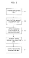
- FIG. 2 is a block diagram illustrating an example of the configuration of the jitter pass element model 7 according to the first embodiment.
- the jitter pass element model 7 includes a parameter setting unit 11, an input jitter amount acquisition unit 12, a jitter transfer function value calculation unit 13, an output jitter amount calculation unit 14, and an output waveform generation unit 15.
- the first acquisition unit corresponds to the parameter setting unit 11.
- the second acquisition unit corresponds to the input jitter amount acquisition unit 12.
- the first calculation unit corresponds to the jitter transfer function value calculation unit 13.
- the second calculation unit corresponds to the output jitter amount calculation unit 14.
- the waveform generation unit corresponds to the output waveform generation unit 15.
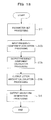
- FIG. 3 is a flowchart illustrating an example of the operation of the circuit simulation apparatus according to the first embodiment.
- the parameter setting unit 11 performs parameter set processing (S11).
- the input jitter amount acquisition unit 12 performs input jitter amount acquisition processing (S12).
- the jitter transfer function value calculation unit 13 performs jitter transfer function value calculation processing (S13).
- the output jitter amount calculation unit 14 performs output jitter amount calculation processing (S14).
- the output waveform generation unit 15 performs output waveform generation processing (S15).
- the parameter setting unit 11 displays a parameter input screen, and sets the attributes of the jitter pass element model 7 of the relevant element according to user inputs on the parameter input screen.
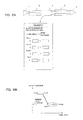
- FIG. 4 is a diagram illustrating an example of the parameter input screen which is displayed by the parameter setting unit 11 according to the first embodiment.
- FIG. 4 illustrates the simulation model of the relevant device, which includes: a sending element model 4; a transmission line model 6 in the subsequent stage; a jitter pass element model 7, or relevant element model, in the subsequent stage; a transmission line model 6 in the subsequent stage; and a receiving element model 4 in the subsequent stage.
- FIG. 4 illustrates the parameter input screen for a user to input the parameters of the jitter pass element model 7.
- the parameter setting unit 11 sets the following parameters:
- the parameter setting unit 11 sets these values as an attribute of the jitter pass element model 7.
- the parameter setting unit 11 sets the jitter transfer function as an attribute of the jitter pass element model 7.
- the jitter transfer function is a frequency characteristic expressed by a line graph, being composed of catalog data or measured data.
- the parameter setting unit 11 also displays the jitter transfer function of an element without jitter amplification or suppression, where input jitter is transferred to the output directly, as an alternative on the parameter input screen.
- the parameter setting unit 11 sets a jitter transfer function that is 1 to across the entire frequency range, as an attribute of the jitter pass element model 7. This parameter set processing makes it possible to discriminate an element without jitter amplification or suppression for the sake of reduced man-hours for input.
- jitter may be added fixedly because of noise and other factors.
- the amount of the jitter to be added is predetermined.
- the parameter setting unit 11 sets the value as an attribute of the jitter pass element model 7.
- the parameter setting unit 11 sets the waveform characteristic of an output signal as an attribute of the jitter pass element model 7 according to user input.
- the waveform characteristic of the output signal includes amplitude and rise/fall time.
- the parameter setting unit 11 sets it as an attribute of the jitter pass element model 7.
- the jitter tolerance has a frequency characteristic which is expressed by a line graph, and is input in terms of the coordinates of a change point or change points as with the jitter transfer function.
- This parameter set processing makes it possible to include the jitter tolerance of the receiving element as one of the conditions for calculating the transfer function of the jitter pass element.
- the frequency characteristic of the jitter tolerance can be input in terms of change points.
- the parameter setting unit 11 sets target jitter type as an attribute of the jitter pass element model 7 according to user input.
- the target jitter type refers to the type of intended jitter among the output jitters of the sending element in the preceding stage of the relevant element.
- the target jitter type is selected from Dj and Rj. This selection is made by the user, based on such factors as the function of the relevant device and the frequency of power supply noise that occurs on the printed circuit board (the jitter frequency of the sending element which typically coincides with the frequency of the power supply noise). Both of Dj and Rj may be selected, and neither may be selected.
- This parameter set processing makes it possible to select the type(s) of jitter(s) to be passed, from among the jitters of the sending element in the preceding stage.
- Some jitter-suppressing elements are considered to suppress all Dj in the element characteristic. For such elements, Dj can be excluded from calculation targets beforehand so that overestimation is avoided of the amount of jitter to pass.
- jitter pass phenomenon When expressing a jitter pass phenomenon, it is first necessary to identify the jitters included in the input signal. Actual waveforms contain various kinds of jitter components (such as random jitter and deterministic jitter). Typical circuit simulation programs, on the other hand, often express jitters that occur when a signal is transmitted through a transmission line and that are output from the sending element separately from each other.
- the output jitter of the sending element in the preceding stage is defined in the catalog specifications of the sending element, and is typically set in the sending element model as parameters.
- the input jitter amount acquisition unit 12 reads and recognizes the parameters of the sending element model as variables (variable processing).
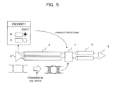
- FIG. 5 is a diagram illustrating an example of the input jitter amount acquisition processing according to the first embodiment.
- the simulation model illustrated in FIG. 5 is the same as that of FIG. 4 .
- FIG. 5 illustrates an attribute (property) display screen of the sending element, the output waveform of the sending element, and the input waveform of the relevant element.
- the Dj and Rj values are preset in the sending element model. The selection of Dj and/or Rj indicates the target jitter type which is set as a property of the jitter pass element by the parameter set processing.
- this input jitter amount acquisition processing it is possible to divide the jitter input to the jitter pass element into the output jitter of the sending element and a transmission line jitter occurring from the transmission line, and process the output jitter as variables. This processing eliminates the need to express the jitter behavior of the sending element, thereby contributing to a reduced amount of calculation.
- the transmission line jitter appears as a waveform deterioration due to transmission line loss, and varies with the transmission line loss. Information on the transmission line jitter therefore may not be recognized by variable processing as with the output jitter of the sending element.
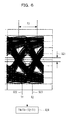
- the input jitter amount acquisition unit 12 observes the eye pattern of the waveform input to the relevant element, and calculates the duration of the area (cross point) where this eye pattern crosses the time axis (cross point duration detection processing), thereby recognizing the cross point duration as the amount of transmission line jitter.
- FIG. 6 is a diagram illustrating an example of the cross point duration detection processing according to the first embodiment. This diagram illustrates the eye pattern of a waveform input to the relevant element.
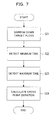
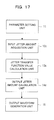
- FIG. 7 is a flowchart illustrating an example of the cross point duration detection processing according to the first embodiment.
- the input jitter amount acquisition unit 12 narrows down target plots in the eye pattern of the waveform input to the relevant element (S21).
- the input jitter amount acquisition unit 12 detects a plot of minimum time T1 in the opening of the target plots (S22).
- the input jitter amount acquisition unit 12 detects a plot of maximum time T2 in the opening of the target plots (S23).
- This input jitter amount acquisition processing makes it possible to recognize the transmission line jitter as the input jitter of the jitter pass element, and use it for subsequent processing.
- the jitter transfer function value calculation processing will be described below.
- the jitter transfer function value calculation processing varies with the types of intended jitter pass elements, which are broadly classified into two types.
- a first type of jitter pass element superimposes a certain jitter on input jitter before output.
- a second type of jitter pass element suppresses input jitter with a certain transfer function before output.
- the jitter transfer function of the first type is 1 to across the entire frequency range.
- the jitter transfer function value calculation unit 13 of the present embodiment determines the target frequency range based on the frequency dependence of the jitter tolerance of a CDR (Clock Data Recovery) circuit in the receiving element at the subsequent stage of the relevant element, and uses a maximum jitter transfer function value in that frequency range.
- CDR Chip Data Recovery
- the jitter transfer function value calculation unit 13 initially performs minimum jitter tolerance extraction processing to extract a point of the minimum jitter tolerance from among the change points of the receiving element's jitter tolerance which is set by the parameter set processing.
- the specific calculation formula for the minimum jitter tolerance extraction processing is given by the following:
- Minimum jitter tolerance MIN(jitter tolerances in all change points).
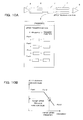
- FIG. 8 is a diagram illustrating an example of the minimum jitter tolerance extraction processing according to the first embodiment.
- the simulation model illustrated in FIG. 8A is the same as that of FIG. 4 .
- FIG. 8A also illustrates an attribute display screen pertaining to the jitter tolerance of the receiving element, or an attribute of the jitter pass element model 7, and
- FIG. 8B illustrates an example of the plot of the jitter tolerance of the receiving element.
- the jitter transfer function value calculation unit 13 extracts the jitter tolerance of Point 3 to Point 4 from the frequency characteristic of the jitter tolerance of the receiving element as the minimum jitter tolerance. According to this minimum jitter tolerance extraction processing, it is possible to extract the minimum jitter tolerance from the change points of the jitter tolerance of the receiving element which are input as parameters, by using a typical MIN function.
- the jitter transfer function value calculation unit 13 performs target jitter frequency extraction processing to extract a frequency of the minimum jitter tolerance which is extracted by the minimum jitter tolerance extraction processing, as a target jitter frequency.
- This target jitter frequency extraction processing is performed for the following two reasons:
- Target jitter frequency MIN(frequencies at minimum jitter tolerance extracted by the minimum jitter tolerance extraction processing).
- FIG. 9 is a diagram illustrating an example of the target jitter frequency extraction processing according to the first embodiment.
- the simulation model illustrated in this diagram is the same as that of FIG. 4 .
- FIG. 9A illustrates an attribute display screen pertaining to the jitter tolerance of the receiving element
- FIG. 9B illustrates an example of the plot of the jitter tolerance of the receiving element.
- the jitter transfer function value calculation unit 13 extracts the frequency of Point 3, which is the minimum frequency among those of Point 3 to Point 4 with the minimum jitter tolerance, as the target jitter frequency.
- this target jitter frequency extraction processing it is possible to narrow the change points of the jitter tolerance of the receiving element which are input as parameters, down to ones pertaining to the minimum jitter tolerance based on the general tendency on the jitter characteristics of jitter pass elements and receiving elements. Then, the frequency to be subjected to the jitter transfer function value calculation can be extracted therefrom by using an ordinary MIN function.
- the jitter transfer function value calculation unit 13 performs target jitter transfer function value calculation processing to calculate the jitter transfer function value of the relevant element at the target jitter frequency which is extracted by the target jitter frequency extraction processing.
- the jitter transfer function value calculation unit 13 calculates the jitter transfer function value at the target jitter frequency by means of linear approximation using the plot of the jitter transfer function which is input as parameters.
- FIG. 10 is a diagram illustrating an example of the target jitter transfer function value calculation processing according to the first embodiment.
- the simulation model illustrated in FIG. 10A is the same as that of FIG. 4 .
- FIG. 10A also illustrates an attribute display screen pertaining to the jitter transfer function, or an attribute of the jitter pass element model 7, and
- FIG. 10B illustrates an example of the plot of the jitter transfer function.
- the jitter transfer function value calculation unit 13 calculates the target jitter transfer function value, i.e., the value of the jitter transfer function at the target jitter frequency (Point 3) by means of linear approximation (interpolation) between Point 2 and Point 3.
- the output jitter amount calculation unit 14 calculates the amount of output jitter based on the numerical values acquired.
- FIG. 11 is a diagram illustrating an example of the output jitter amount calculation processing according to the first embodiment.
- the simulation model illustrated in FIG. 11 is the same as that of FIG. 4 .
- FIG. 11 illustrates an attribute display screen of the sending element, the output waveform of the sending element, the input waveform of the relevant element, and the output waveform of the relevant element.
- the Dj and Rj values are set in the sending element model.
- the "select" indicates that the value is set as an attribute of the relevant element by the parameter set processing.
- the output jitter amount calculation processing makes it possible to incorporate the formula for calculating the amount of output jitter into the simulation model, thereby calculating the amount of jitter to be output from the jitter pass element and expressing the behavior of the same.
- the jitter pass element model 7 includes an output buffer model and a waveform display function as the output waveform generation unit 15.
- the output buffer model generates a waveform.
- the waveform display function adds the amount of output jitter calculated by the output jitter amount calculation processing to the generated waveform, thereby generating an output waveform.
- the output buffer model is configured as an ordinary behavior model which is composed of current sources and resistances. Behavior models express amplitudes and output impedances by adjusting the current sources and resistances, and are incapable of jitter expression.
- the output waveform generation unit 15 of the present embodiment therefore provides a pseudo-expression of the jitter phenomenon by using the waveform display function.
- FIG. 12 is a diagram illustrating an example of the output waveform generation processing according to the first embodiment.
- the simulation model illustrated in FIG. 12 is the same as that of FIG. 4 .
- FIG. 12 also illustrates an example of the output waveform of the jitter pass element model 7.
- the output waveform generation unit 15 superimposes jitter-free waveforms on each other to generate an eye pattern, and thickens the eye pattern into an output waveform as much as the amount of output jitter in the direction of the time axis.
- One of the conventional techniques for expressing the behavior of a jitter pass element is to use transistor models. Elements having a jitter-suppressing effect, however, require transistor models of vast scale to model with. An enormous amount of simulation time is required to express the frequency dependence of PLLs (Phase Locked Loops) or the like. It has thus net been possible to practice the technique. According to the present embodiment, it is possible to express a jitter pass element with a behavior model and perform simulations thereon.
- PLLs Phase Locked Loops
- the present embodiment also makes it possible to verify an entire signal transmission system including a jitter pass element by a single circuit simulation, thereby reducing the circuit simulation time of a signal transmission system with high speed signals to or below 1/10.
- FIG. 13 is a block diagram illustrating an example of the configuration of a circuit simulation apparatus according to a second embodiment of the present invention.
- the same reference numerals as in FIG. 1 represent components identical or equivalent to those illustrated in FIG. 1 , and description thereof will be omitted.
- the circuit simulation apparatus in this diagram includes a receiving element model 5b instead of the receiving element model 5, and a jitter pass element model 7b instead of the jitter pass element model 7.
- FIG. 14 is a block diagram illustrating an example of the configuration of the jitter pass element model 7b according to the second embodiment.
- the same reference numerals as in FIG. 2 represent components identical or equivalent to those illustrated in FIG. 2 , and description thereof will be omitted.
- the jitter pass element model 7b includes a parameter setting unit 11b instead of the parameter setting unit 11, and a jitter transfer function value calculation unit 13b instead of the jitter transfer function value calculation unit 13.
- the circuit simulation apparatus makes the same operation as in the first embodiment, with only differences in the contents of the parameter set processing and the jitter transfer function value calculation processing.
- the parameter setting unit 11 sets the user-input information pertaining to the jitter tolerance of the receiving element into the jitter pass element model 7.
- the jitter transfer function value calculation unit 13 acquires the jitter tolerance of the receiving element which is set in the jitter pass element model 7, and calculates the jitter transfer function value of the jitter pass element. This technique, however, makes it inconvenient to use the models as a library since the information needs to be input each time the receiving element is changed.
- the parameter setting unit 11b does not set the parameters pertaining to the jitter tolerance of the receiving element as an attribute of the jitter pass element model 7b. Instead, the receiving element model 5b sets the user-input parameters pertaining to the jitter tolerance of the receiving element as an attribute of the receiving element model 5b.
- FIG. 15 is a diagram illustrating an example of the jitter transfer function value calculation processing according to the second embodiment.
- the simulation model illustrated in FIG. 15 is the same as that of FIG. 4 .
- FIG. 15 illustrates a screen for displaying jitter tolerance which is an attribute of the receiving element.
- the jitter transfer function value calculation unit 13b identifies the receiving element model connected to the subsequent stage of the relevant element, acquires the receiving element's jitter tolerance which is set in the receiving element model, and calculates the jitter transfer function value of the jitter pass element.
- the information on the characteristics of the element models is set into the respective models. This facilitates utilizing the models as a library.
- FIG. 16 is a block diagram illustrating an example of the configuration of a circuit simulation apparatus according to a third embodiment of the present invention.
- the same reference numerals as in FIG. 1 represent components identical or equivalent to those illustrated in FIG. 1 , and description thereof will be omitted.
- the circuit simulation apparatus in this diagram includes a jitter pass element model 7c instead of the jitter pass element model 7.
- FIG. 17 is a block diagram illustrating an example of the configuration of the jitter pass element model 7c according to the third embodiment.
- the same reference numerals as in FIG. 2 represent components identical or equivalent to those illustrated in FIG. 2 , and description thereof will be omitted.
- the jitter pass element model 7c includes an input jitter amount acquisition unit 12c instead of the input jitter amount acquisition unit 12, a jitter transfer function value calculation unit 13c instead of the jitter transfer function value calculation unit 13, and an output jitter amount calculation unit 14c instead of the output jitter amount calculation unit 14.
- the characteristic of the jitter pass element is expressed by using the numerical values that are defined by the sending element in the preceding stage and the receiving element in the subsequent stage.
- An accurate expression of the jitter behavior requires that the jitter be analyzed for frequency components.
- FIG. 18 is a flowchart illustrating an example of the operation of the jitter pass element model 7c according to the third embodiment.
- the parameter setting unit 11 performs the same parameter set processing as in the first embodiment (S11).
- the input jitter amount acquisition unit 12c performs input frequency component acquisition processing for acquiring the frequency components of the jitter input to the relevant element (S12c).
- the jitter transfer function value calculation unit 13c performs output frequency component calculation processing for calculating the frequency components of jitter to be output from the relevant element by using a jitter transfer function (S13c).
- the output jitter amount calculation unit 14c performs output jitter amount calculation processing for calculating the amount of jitter to be output from the relevant element by combining the frequency components of the jitter to be output from the relevant element (S14c). Then, the output waveform generation unit 15 performs the same output waveform generation processing as in the first embodiment (S15), and ends this flow.
- the input frequency component acquisition processing will be described below.
- the input jitter amount acquisition unit 12c acquires numerical data that expresses the frequency components of the input jitter contained in the input signal of the relevant element.
- This numerical data includes the frequencies of the frequency components of the jitter (jitter frequencies) and energy in pairs.
- this numerical data will be referred to as the spectrum of the jitter.
- FIG. 19 is a diagram illustrating an example of the input frequency component acquisition processing according to the third embodiment.
- FIG. 19 illustrates an input signal to the jitter pass element model 7c, the jitter pass element model 7c, and an output signal from the jitter pass element model 7c.
- FIG. 19 also illustrates the plot of the spectrum of jitter contained in the input signal.
- FIG. 19 also illustrates the numerical data on the spectrum which is input by the user.
- the numerical data on the spectrum is obtained by measurement or by a simulation based on the input signal to the relevant element, i.e., the output signal of the sending element that is connected to the preceding stage.
- the input jitter amount acquisition unit 12c acquires frequencies f1, f2, f3, and f4, and corresponding jitter amplitudes A1, A2, A3, and A4 from the numerical data on the spectrum.
- the jitter transfer function value calculation unit 13c calculates the energy of the jitter to be output from the jitter pass element (output jitter energy) with respect to each of the jitter frequencies based on the spectrum of the input jitter and the jitter transfer function.
- FIG. 20 is a diagram illustrating an example of the output frequency component calculation processing according to the third embodiment.
- FIG. 20 illustrates an input signal to the jitter pass element model 7c, the jitter pass element model 7c, and an output signal from the jitter pass element model 7c.
- FIG. 20 also illustrates numerical data on the spectrum.
- FIG. 20 also illustrates the jitter transfer function.
- the jitter transfer function values at frequencies f1, f2, f3, and f4 shall be tf1, tf1, tf2, and tf3, respectively.
- FIG. 21 illustrates equations for an example of the output frequency component calculation processing according to the third embodiment.
- the output jitter energies jo(f1), jo(f2), jo(f3), and jo(f4) at the respective frequencies f1, f2, f3, and f4 are determined by these functions.
- the output jitter amount calculation unit 14c integrates the frequency components of the output jitter calculated by the output frequency component calculation processing with respect to the frequency across the entire pass band, thereby calculating the amount of output jitter along the time axis.
- FIG. 22 illustrates an equation for an example of the output jitter amount calculation processing according to the third embodiment.
- the amount of output jitter j is calculated by integrating jo(f) with respect to the frequency across the entire pass band.
- the frequency analysis function is incorporated into the jitter pass element model 7c so that simulations can be made with higher precision.
- Each of the foregoing embodiments may be applied to techniques of signal waveform analysis for calculating a comprehensive transmission margin with consideration given to factors that can deteriorate transmission quality.
- a program for making a computer that constitutes the circuit simulation apparatus perform the foregoing steps may be provided as a circuit simulation program.
- the program may be stored in a computer-readable recording medium so that it can be executed by a computer that constitutes the circuit simulation apparatus.
- Examples of the computer-readable recording medium include: internal storage devices implemented inside the computer such as ROM and RAM; portable recording media such as a CD-ROM, flexible disk, DVD disk, magneto-optical disk, and IC card; databases for storing computer programs, and other computers and their databases; and even online transmission media.
- the circuit simulation apparatus the medium containing a circuit simulation program, and the circuit simulation method disclosed therein, it is possible to perform a circuit simulation on a circuit including a jitter pass element with high efficiency.
- the various features may be implemented in hardware, or as software modules running on one or more processors. Features of one aspect may be applied to any o the other aspects.
- the invention also provides a computer program or a computer program product for carrying out any of the methods described herein, and a computer readable medium having stored thereon a program for carrying out any of the methods described herein.
- a computer program embodying the invention may be stored on a computer-readable medium, or it could, for example, be in the form of a signal such as a downloadable data signal provided from an Internet website, or it could be in any other form.
Landscapes
- Engineering & Computer Science (AREA)
- Computer Hardware Design (AREA)
- Physics & Mathematics (AREA)
- Theoretical Computer Science (AREA)
- Microelectronics & Electronic Packaging (AREA)
- Evolutionary Computation (AREA)
- Geometry (AREA)
- General Engineering & Computer Science (AREA)
- General Physics & Mathematics (AREA)
- Dc Digital Transmission (AREA)
Abstract
A circuit simulation apparatus includes a first acquisition unit that acquires information on a jitter transfer function of a jitter pass element with respect to a predetermined frequency band, a second acquisition unit that acquires information pertaining to input jitter to the jitter pass element, a first calculation unit that determines a jitter frequency based on the information acquired by the first acquisition unit or the second acquisition unit to calculate a jitter transfer function value which is a value of the jitter transfer function acquired by the first acquisition unit at the jitter frequency, and a second calculation unit that calculates output jitter from the jitter pass element based on the information pertaining to the input jitter acquired by the second acquisition unit and the jitter transfer function value calculated by the first calculation unit.
Description
- The present invention relates to a circuit simulation apparatus for performing a circuit simulation pertaining to jitter that passes through an element, a medium containing a circuit simulation program, a circuit simulation method.
- The amount of information processing demanded of digital electronic apparatuses has been on the increase in recent years. Signal speeds inside the apparatuses have increased accordingly, with the propensity for smaller transmission margins. It has therefore been necessary to estimate the transmission margins accurately, putting a large number of factors for margin deterioration together. In particular, a phase shift (jitter) in elements and transmission systems has been a factor of ever increasing significance.
- Among the conventional technologies is a method of analyzing a transmission line, in which a rough estimation of the amount of jitter is calculated from an eye pattern that is obtained by transmitting short bit patterns through the transmission line. There is also a measuring apparatus which calculates the jitter transfer function, bit error rate, and jitter tolerance of a Device Under Test (DUT) with high efficiency (refer to, e.g., Patent Document 1: Japanese. Laid-Open Patent Publication No.
2007-292520 WO 2003/073680 ). - It is not possible, however, to model elements that have a jitter transfer function (jitter pass elements), such as an optical module, buffer, and repeater, by using ordinary waveform simulators. As employed herein, the jitter transfer function of a jitter pass element refers to the ratio of output jitter to input jitter thereof, and is expressed as a frequency characteristic.
- A signal transmission system is thus divided into systems preceding and subsequent to a jitter pass element, and the systems are subjected to respective circuit simulations. The jitter determined by the circuit simulation on the system in the preceding stage is then added to the jitter determined by the circuit simulation on the system in the subsequent stage, whereby the result of the entire circuit simulation is obtained.
- This circuit simulation method has a significant drawback in terms of man-hours due to reasons such as complicated modeling and the incapability of comprehensive simulation.
- It is desirable to provide a circuit simulation apparatus for performing a circuit simulation on a circuit including a jitter pass element with high efficiency, a medium containing a circuit simulation program, a circuit simulation method, a medium containing a circuit simulation modeling program, an electronic circuit, and an electronic circuit board.
- According to embodiments of an aspect of the invention, there is provided a circuit simulation apparatus for performing a circuit simulation using a jitter pass element model that is a model of a jitter pass element, the jitter pass element being an element for jitter to pass through, the apparatus including: a first acquisition unit that acquires information on a jitter transfer function of the jitter pass element with respect to a predetermined frequency band; a second acquisition unit that acquires information pertaining to input jitter to the jitter pass element; a first calculation unit that determines a jitter frequency based on the information acquired by the first acquisition unit or the second acquisition unit to calculate a jitter transfer function value which is a value of the jitter transfer function acquired by the first acquisition unit at the jitter frequency; and a second calculation unit that calculates output jitter from the jitter pass element based on the information pertaining to the input jitter acquired by the second acquisition unit and the jitter transfer function value calculated by the first calculation unit.
- The desirable outcomes and advantages of the invention will be realized and attained by means of the elements and combinations particularly pointed out in the claims.
- It is to be understood that both the foregoing general description and the following detailed description are exemplary and explanatory and are not restrictive of the invention, as claimed.
- Preferred features of the present invention will now be described, purely by way of example, with reference to the accompanying drawings, in which:-
-
FIG. 1 is a block diagram illustrating an example of the configuration of a circuit simulation apparatus according to a first embodiment of the present invention; -
FIG. 2 is a block diagram illustrating an example of the configuration of a jitterpass element model 7 according to the first embodiment; -
FIG. 3 is a flowchart illustrating an example of the operation of the circuit simulation apparatus according to the first embodiment; -
FIG. 4 is a diagram illustrating an example of a parameter input screen which is displayed by aparameter setting unit 11 according to the first embodiment; -
FIG. 5 is a diagram illustrating an example of input jitter amount acquisition processing according to the first embodiment; -
FIG. 6 is a diagram illustrating an example of cross point duration detection processing according to the first embodiment; -
FIG. 7 is a flowchart illustrating an example of the cross point duration detection processing according to the first embodiment; -
FIG. 8 is a diagram illustrating an example of minimum jitter tolerance extraction processing according to the first embodiment; -
FIG. 9 is a diagram illustrating an example of target jitter frequency extraction processing according to the first embodiment; -
FIG. 10 is a diagram illustrating an example of target jitter transfer function value calculation processing according to the first embodiment; -
FIG. 11 is a diagram illustrating an example of output jitter amount calculation processing according to the first embodiment; -
FIG. 12 is a diagram illustrating an example of output waveform generation processing according to the first embodiment; -
FIG. 13 is a block diagram illustrating an example of the configuration of a circuit simulation apparatus according to a second embodiment of the present invention; -
FIG. 14 is a block diagram illustrating an example of the configuration of a jitterpass element model 7b according to the second embodiment; -
FIG. 15 is a diagram illustrating an example of jitter transfer function value calculation processing according to the second embodiment; -
FIG. 16 is a block diagram illustrating an example of the configuration of a circuit simulation apparatus according to the second embodiment; -
FIG. 17 is a block diagram illustrating an example of the configuration of a jitterpass element model 7c according to a third embodiment of the present invention; -
FIG. 18 is a flowchart illustrating an example of the operation of the jitterpass element model 7c according to the third embodiment; -
FIG. 19 is a diagram illustrating an example of input frequency component acquisition processing according to the third embodiment; -
FIG. 20 is a diagram illustrating an example of output frequency component calculation processing according to the third embodiment; -
FIG. 21 is a chart illustrating equations for an example of the output frequency component calculation processing according to the third embodiment; and -
FIG. 22 is a chart illustrating an equation for an example of output jitter amount calculation processing according to the third embodiment. - Hereinafter, embodiments of the present invention will be described with reference to the drawings.
- Description will be given of the configuration of a circuit simulation apparatus according to the present embodiment.
-
FIG. 1 is a block diagram illustrating an example of the configuration of the circuit simulation apparatus according to a first embodiment of the present invention. The circuit simulation apparatus includes a circuitdata storing unit 1, acontrol unit 2, and amodel library 3. Themodel library 3 includes asending element model 4, areceiving element model 5, atransmission line model 6, and a jitterpass element model 7. Hereinafter, a device to be subjected to a circuit simulation will be referred to as a relevant device. The relevant device includes a sending element, a transmission line in the subsequent stage, a jitter pass element in the subsequent stage, a transmission line in the subsequent stage, and a receiving element in the subsequent stage. The jitter pass element in the relevant device will be referred to as a relevant element. - Circuit data on the relevant device which is designed by using the models in the
model library 3 is stored in the circuitdata storing unit 1. Thecontrol unit 2 controls a circuit simulation on the circuit data stored in the circuitdata storing unit 1, by using the models in themodel library 3. An example of the circuit simulation apparatus is a computer having a CPU (Central Processing Unit) and a storage device. An example of the circuitdata storing unit 1 is the storage device. Examples of thecontrol unit 2 and themodel library 3 are programs which are stored in the storage device and executed by the CPU. -
FIG. 2 is a block diagram illustrating an example of the configuration of the jitterpass element model 7 according to the first embodiment. The jitterpass element model 7 includes aparameter setting unit 11, an input jitteramount acquisition unit 12, a jitter transfer functionvalue calculation unit 13, an output jitteramount calculation unit 14, and an outputwaveform generation unit 15. The first acquisition unit corresponds to theparameter setting unit 11. The second acquisition unit corresponds to the input jitteramount acquisition unit 12. The first calculation unit corresponds to the jitter transfer functionvalue calculation unit 13. The second calculation unit corresponds to the output jitteramount calculation unit 14. The waveform generation unit corresponds to the outputwaveform generation unit 15. - Next, the operation of the circuit simulation apparatus according to the present embodiment will be overviewed.
-
FIG. 3 is a flowchart illustrating an example of the operation of the circuit simulation apparatus according to the first embodiment. Theparameter setting unit 11 performs parameter set processing (S11). Next, the input jitteramount acquisition unit 12 performs input jitter amount acquisition processing (S12). Then, the jitter transfer functionvalue calculation unit 13 performs jitter transfer function value calculation processing (S13). Subsequently, the output jitteramount calculation unit 14 performs output jitter amount calculation processing (S14). Then, the outputwaveform generation unit 15 performs output waveform generation processing (S15). - The parameter set processing will be described below.
- The
parameter setting unit 11 displays a parameter input screen, and sets the attributes of the jitterpass element model 7 of the relevant element according to user inputs on the parameter input screen.FIG. 4 is a diagram illustrating an example of the parameter input screen which is displayed by theparameter setting unit 11 according to the first embodiment.FIG. 4 illustrates the simulation model of the relevant device, which includes: a sendingelement model 4; atransmission line model 6 in the subsequent stage; a jitterpass element model 7, or relevant element model, in the subsequent stage; atransmission line model 6 in the subsequent stage; and a receivingelement model 4 in the subsequent stage.FIG. 4 illustrates the parameter input screen for a user to input the parameters of the jitterpass element model 7. For the attributes of the jitterpass element model 7, theparameter setting unit 11 sets the following parameters: - (1) The limit values of input amplitude (MIN, MAX);
- (2) The jitter transfer function of the relevant element;
- (3) Additional jitter;
- (4) The waveform characteristic of the output signal;
- (5) The jitter tolerance of the receiving element; and
- (6) Target jitter type.
- When the limit values of the input amplitude are input by the user, the
parameter setting unit 11 sets these values as an attribute of the jitterpass element model 7. - When the coordinates of a change point or change points in the frequency characteristic of a jitter transfer function are input by the user, the
parameter setting unit 11 sets the jitter transfer function as an attribute of the jitterpass element model 7. The jitter transfer function is a frequency characteristic expressed by a line graph, being composed of catalog data or measured data. - The
parameter setting unit 11 also displays the jitter transfer function of an element without jitter amplification or suppression, where input jitter is transferred to the output directly, as an alternative on the parameter input screen. When this alternative is selected by the user, theparameter setting unit 11 sets a jitter transfer function that is 1 to across the entire frequency range, as an attribute of the jitterpass element model 7. This parameter set processing makes it possible to discriminate an element without jitter amplification or suppression for the sake of reduced man-hours for input. - In some jitter pass elements, jitter may be added fixedly because of noise and other factors. In this case, the amount of the jitter to be added (additional jitter) is predetermined. When additional jitter is input by the user, the
parameter setting unit 11 therefore sets the value as an attribute of the jitterpass element model 7. - The
parameter setting unit 11 sets the waveform characteristic of an output signal as an attribute of the jitterpass element model 7 according to user input. The waveform characteristic of the output signal includes amplitude and rise/fall time. - When the jitter tolerance of the receiving element is input by the user from the parameter input screen, the
parameter setting unit 11 sets it as an attribute of the jitterpass element model 7. The jitter tolerance has a frequency characteristic which is expressed by a line graph, and is input in terms of the coordinates of a change point or change points as with the jitter transfer function. This parameter set processing makes it possible to include the jitter tolerance of the receiving element as one of the conditions for calculating the transfer function of the jitter pass element. The frequency characteristic of the jitter tolerance can be input in terms of change points. - The
parameter setting unit 11 sets target jitter type as an attribute of the jitterpass element model 7 according to user input. The target jitter type refers to the type of intended jitter among the output jitters of the sending element in the preceding stage of the relevant element. The target jitter type is selected from Dj and Rj. This selection is made by the user, based on such factors as the function of the relevant device and the frequency of power supply noise that occurs on the printed circuit board (the jitter frequency of the sending element which typically coincides with the frequency of the power supply noise). Both of Dj and Rj may be selected, and neither may be selected. - This parameter set processing makes it possible to select the type(s) of jitter(s) to be passed, from among the jitters of the sending element in the preceding stage. Some jitter-suppressing elements are considered to suppress all Dj in the element characteristic. For such elements, Dj can be excluded from calculation targets beforehand so that overestimation is avoided of the amount of jitter to pass.
- The input jitter amount acquisition processing will be described below.
- When expressing a jitter pass phenomenon, it is first necessary to identify the jitters included in the input signal. Actual waveforms contain various kinds of jitter components (such as random jitter and deterministic jitter). Typical circuit simulation programs, on the other hand, often express jitters that occur when a signal is transmitted through a transmission line and that are output from the sending element separately from each other.
- Of these, the output jitter of the sending element in the preceding stage is defined in the catalog specifications of the sending element, and is typically set in the sending element model as parameters. The input jitter
amount acquisition unit 12 reads and recognizes the parameters of the sending element model as variables (variable processing). -
FIG. 5 is a diagram illustrating an example of the input jitter amount acquisition processing according to the first embodiment. The simulation model illustrated inFIG. 5 is the same as that ofFIG. 4 .FIG. 5 illustrates an attribute (property) display screen of the sending element, the output waveform of the sending element, and the input waveform of the relevant element. Among the attributes of the sending element, the Dj and Rj values are preset in the sending element model. The selection of Dj and/or Rj indicates the target jitter type which is set as a property of the jitter pass element by the parameter set processing. - According to this input jitter amount acquisition processing, it is possible to divide the jitter input to the jitter pass element into the output jitter of the sending element and a transmission line jitter occurring from the transmission line, and process the output jitter as variables. This processing eliminates the need to express the jitter behavior of the sending element, thereby contributing to a reduced amount of calculation.
- The transmission line jitter appears as a waveform deterioration due to transmission line loss, and varies with the transmission line loss. Information on the transmission line jitter therefore may not be recognized by variable processing as with the output jitter of the sending element. The input jitter
amount acquisition unit 12 observes the eye pattern of the waveform input to the relevant element, and calculates the duration of the area (cross point) where this eye pattern crosses the time axis (cross point duration detection processing), thereby recognizing the cross point duration as the amount of transmission line jitter. -
FIG. 6 is a diagram illustrating an example of the cross point duration detection processing according to the first embodiment. This diagram illustrates the eye pattern of a waveform input to the relevant element.FIG. 7 is a flowchart illustrating an example of the cross point duration detection processing according to the first embodiment. The input jitteramount acquisition unit 12 narrows down target plots in the eye pattern of the waveform input to the relevant element (S21). Next, the input jitteramount acquisition unit 12 detects a plot of minimum time T1 in the opening of the target plots (S22). Then, the input jitteramount acquisition unit 12 detects a plot of maximum time T2 in the opening of the target plots (S23). Subsequently, the input jitteramount acquisition unit 12 calculates the cross point duration T4 = (T3 - (T2 - T1)), where T3 is the period of the input waveform (S24), and ends this flow. - This input jitter amount acquisition processing makes it possible to recognize the transmission line jitter as the input jitter of the jitter pass element, and use it for subsequent processing.
- The jitter transfer function value calculation processing will be described below.
- The jitter transfer function value calculation processing varies with the types of intended jitter pass elements, which are broadly classified into two types. A first type of jitter pass element superimposes a certain jitter on input jitter before output. A second type of jitter pass element suppresses input jitter with a certain transfer function before output. The jitter transfer function of the first type is 1 to across the entire frequency range.
- Next, the jitter transfer function value calculation processing of second type will be described in detail.
- For a second type of jitter pass element, the frequency dependence of the jitter transfer function is often given as catalog data or measured data. It is technically quite difficult, however, to express the jitter frequency dependence with ordinary simulation models. The jitter transfer function
value calculation unit 13 of the present embodiment determines the target frequency range based on the frequency dependence of the jitter tolerance of a CDR (Clock Data Recovery) circuit in the receiving element at the subsequent stage of the relevant element, and uses a maximum jitter transfer function value in that frequency range. - The jitter transfer function
value calculation unit 13 initially performs minimum jitter tolerance extraction processing to extract a point of the minimum jitter tolerance from among the change points of the receiving element's jitter tolerance which is set by the parameter set processing. The specific calculation formula for the minimum jitter tolerance extraction processing is given by the following: - Minimum jitter tolerance = MIN(jitter tolerances in all change points).
-
FIG. 8 is a diagram illustrating an example of the minimum jitter tolerance extraction processing according to the first embodiment. The simulation model illustrated inFIG. 8A is the same as that ofFIG. 4 .FIG. 8A also illustrates an attribute display screen pertaining to the jitter tolerance of the receiving element, or an attribute of the jitterpass element model 7, andFIG. 8B illustrates an example of the plot of the jitter tolerance of the receiving element. - In this example, the jitter transfer function
value calculation unit 13 extracts the jitter tolerance ofPoint 3 to Point 4 from the frequency characteristic of the jitter tolerance of the receiving element as the minimum jitter tolerance. According to this minimum jitter tolerance extraction processing, it is possible to extract the minimum jitter tolerance from the change points of the jitter tolerance of the receiving element which are input as parameters, by using a typical MIN function. - Next, the jitter transfer function
value calculation unit 13 performs target jitter frequency extraction processing to extract a frequency of the minimum jitter tolerance which is extracted by the minimum jitter tolerance extraction processing, as a target jitter frequency. This target jitter frequency extraction processing is performed for the following two reasons: - (1) Jitter pass elements typically have the characteristic that the jitter transfer function value increases with decreasing frequency; and
- (2) Receiving elements having a built-in CDR typically decrease in jitter tolerance with increasing jitter frequency, and show a constant tolerance value above a certain frequency.
- The specific calculation formula for the target jitter frequency extraction processing is given by the following:
- Target jitter frequency = MIN(frequencies at minimum jitter tolerance extracted by the minimum jitter tolerance extraction processing).
-
FIG. 9 is a diagram illustrating an example of the target jitter frequency extraction processing according to the first embodiment. The simulation model illustrated in this diagram is the same as that ofFIG. 4 .FIG. 9A illustrates an attribute display screen pertaining to the jitter tolerance of the receiving element, andFIG. 9B illustrates an example of the plot of the jitter tolerance of the receiving element. - In this example, the jitter transfer function
value calculation unit 13 extracts the frequency ofPoint 3, which is the minimum frequency among those ofPoint 3 to Point 4 with the minimum jitter tolerance, as the target jitter frequency. - According to this target jitter frequency extraction processing, it is possible to narrow the change points of the jitter tolerance of the receiving element which are input as parameters, down to ones pertaining to the minimum jitter tolerance based on the general tendency on the jitter characteristics of jitter pass elements and receiving elements. Then, the frequency to be subjected to the jitter transfer function value calculation can be extracted therefrom by using an ordinary MIN function.
- Next, the jitter transfer function
value calculation unit 13 performs target jitter transfer function value calculation processing to calculate the jitter transfer function value of the relevant element at the target jitter frequency which is extracted by the target jitter frequency extraction processing. Here, the jitter transfer functionvalue calculation unit 13 calculates the jitter transfer function value at the target jitter frequency by means of linear approximation using the plot of the jitter transfer function which is input as parameters. -
FIG. 10 is a diagram illustrating an example of the target jitter transfer function value calculation processing according to the first embodiment. The simulation model illustrated inFIG. 10A is the same as that ofFIG. 4 .FIG. 10A also illustrates an attribute display screen pertaining to the jitter transfer function, or an attribute of the jitterpass element model 7, andFIG. 10B illustrates an example of the plot of the jitter transfer function. - In this example, the jitter transfer function
value calculation unit 13 calculates the target jitter transfer function value, i.e., the value of the jitter transfer function at the target jitter frequency (Point 3) by means of linear approximation (interpolation) betweenPoint 2 andPoint 3. - The output jitter amount calculation processing will be described below.
- The output jitter
amount calculation unit 14 calculates the amount of output jitter based on the numerical values acquired. The formula for calculating the amount of output jitter is given by the following:
-
FIG. 11 is a diagram illustrating an example of the output jitter amount calculation processing according to the first embodiment. The simulation model illustrated inFIG. 11 is the same as that ofFIG. 4 .FIG. 11 illustrates an attribute display screen of the sending element, the output waveform of the sending element, the input waveform of the relevant element, and the output waveform of the relevant element. Among the attributes of the sending element in this diagram, the Dj and Rj values are set in the sending element model. The "select" indicates that the value is set as an attribute of the relevant element by the parameter set processing. The output jitter amount calculation processing makes it possible to incorporate the formula for calculating the amount of output jitter into the simulation model, thereby calculating the amount of jitter to be output from the jitter pass element and expressing the behavior of the same. - Next, the output waveform generation processing will be described.
- The jitter
pass element model 7 includes an output buffer model and a waveform display function as the outputwaveform generation unit 15. The output buffer model generates a waveform. The waveform display function adds the amount of output jitter calculated by the output jitter amount calculation processing to the generated waveform, thereby generating an output waveform. - The output buffer model is configured as an ordinary behavior model which is composed of current sources and resistances. Behavior models express amplitudes and output impedances by adjusting the current sources and resistances, and are incapable of jitter expression. The output
waveform generation unit 15 of the present embodiment therefore provides a pseudo-expression of the jitter phenomenon by using the waveform display function. -
FIG. 12 is a diagram illustrating an example of the output waveform generation processing according to the first embodiment. The simulation model illustrated inFIG. 12 is the same as that ofFIG. 4 .FIG. 12 also illustrates an example of the output waveform of the jitterpass element model 7. Here, the outputwaveform generation unit 15 superimposes jitter-free waveforms on each other to generate an eye pattern, and thickens the eye pattern into an output waveform as much as the amount of output jitter in the direction of the time axis. - One of the conventional techniques for expressing the behavior of a jitter pass element is to use transistor models. Elements having a jitter-suppressing effect, however, require transistor models of vast scale to model with. An enormous amount of simulation time is required to express the frequency dependence of PLLs (Phase Locked Loops) or the like. It has thus net been possible to practice the technique. According to the present embodiment, it is possible to express a jitter pass element with a behavior model and perform simulations thereon.
- The present embodiment also makes it possible to verify an entire signal transmission system including a jitter pass element by a single circuit simulation, thereby reducing the circuit simulation time of a signal transmission system with high speed signals to or below 1/10.
-
FIG. 13 is a block diagram illustrating an example of the configuration of a circuit simulation apparatus according to a second embodiment of the present invention. In this diagram, the same reference numerals as inFIG. 1 represent components identical or equivalent to those illustrated inFIG. 1 , and description thereof will be omitted. As compared to the circuit simulation apparatus inFIG. 1 , the circuit simulation apparatus in this diagram includes a receivingelement model 5b instead of the receivingelement model 5, and a jitterpass element model 7b instead of the jitterpass element model 7. -
FIG. 14 is a block diagram illustrating an example of the configuration of the jitterpass element model 7b according to the second embodiment. In this diagram, the same reference numerals as inFIG. 2 represent components identical or equivalent to those illustrated inFIG. 2 , and description thereof will be omitted. As compared to the jitterpass element model 7, the jitterpass element model 7b includes aparameter setting unit 11b instead of theparameter setting unit 11, and a jitter transfer functionvalue calculation unit 13b instead of the jitter transfer functionvalue calculation unit 13. - The circuit simulation apparatus according to the present embodiment makes the same operation as in the first embodiment, with only differences in the contents of the parameter set processing and the jitter transfer function value calculation processing.
- In the parameter set processing of the first embodiment, the
parameter setting unit 11 sets the user-input information pertaining to the jitter tolerance of the receiving element into the jitterpass element model 7. In the jitter transfer function value calculation processing of the first embodiment, the jitter transfer functionvalue calculation unit 13 acquires the jitter tolerance of the receiving element which is set in the jitterpass element model 7, and calculates the jitter transfer function value of the jitter pass element. This technique, however, makes it inconvenient to use the models as a library since the information needs to be input each time the receiving element is changed. - The parameter set processing according to the present embodiment will be described below.
- The
parameter setting unit 11b does not set the parameters pertaining to the jitter tolerance of the receiving element as an attribute of the jitterpass element model 7b. Instead, the receivingelement model 5b sets the user-input parameters pertaining to the jitter tolerance of the receiving element as an attribute of the receivingelement model 5b. - Now, description will be given of the jitter transfer function value calculation processing according to the present embodiment.
-
FIG. 15 is a diagram illustrating an example of the jitter transfer function value calculation processing according to the second embodiment. The simulation model illustrated inFIG. 15 is the same as that ofFIG. 4 .FIG. 15 illustrates a screen for displaying jitter tolerance which is an attribute of the receiving element. - In the jitter transfer function value calculation processing of the present embodiment, the jitter transfer function
value calculation unit 13b identifies the receiving element model connected to the subsequent stage of the relevant element, acquires the receiving element's jitter tolerance which is set in the receiving element model, and calculates the jitter transfer function value of the jitter pass element. - According to the present embodiment, the information on the characteristics of the element models is set into the respective models. This facilitates utilizing the models as a library.
-
FIG. 16 is a block diagram illustrating an example of the configuration of a circuit simulation apparatus according to a third embodiment of the present invention. In this diagram, the same reference numerals as inFIG. 1 represent components identical or equivalent to those illustrated inFIG. 1 , and description thereof will be omitted. As compared to the circuit simulation apparatus inFIG. 1 , the circuit simulation apparatus in this diagram includes a jitterpass element model 7c instead of the jitterpass element model 7. -
FIG. 17 is a block diagram illustrating an example of the configuration of the jitterpass element model 7c according to the third embodiment. In this diagram, the same reference numerals as inFIG. 2 represent components identical or equivalent to those illustrated inFIG. 2 , and description thereof will be omitted. As compared to the jitterpass element model 7, the jitterpass element model 7c includes an input jitteramount acquisition unit 12c instead of the input jitteramount acquisition unit 12, a jitter transfer functionvalue calculation unit 13c instead of the jitter transfer functionvalue calculation unit 13, and an output jitteramount calculation unit 14c instead of the output jitteramount calculation unit 14. - In the circuit simulation apparatus according to the first embodiment, the characteristic of the jitter pass element is expressed by using the numerical values that are defined by the sending element in the preceding stage and the receiving element in the subsequent stage. An accurate expression of the jitter behavior, however, requires that the jitter be analyzed for frequency components.
-
FIG. 18 is a flowchart illustrating an example of the operation of the jitterpass element model 7c according to the third embodiment. Theparameter setting unit 11 performs the same parameter set processing as in the first embodiment (S11). Next, the input jitteramount acquisition unit 12c performs input frequency component acquisition processing for acquiring the frequency components of the jitter input to the relevant element (S12c). Then, the jitter transfer functionvalue calculation unit 13c performs output frequency component calculation processing for calculating the frequency components of jitter to be output from the relevant element by using a jitter transfer function (S13c). Subsequently, the output jitteramount calculation unit 14c performs output jitter amount calculation processing for calculating the amount of jitter to be output from the relevant element by combining the frequency components of the jitter to be output from the relevant element (S14c). Then, the outputwaveform generation unit 15 performs the same output waveform generation processing as in the first embodiment (S15), and ends this flow. - The input frequency component acquisition processing will be described below.
- In the input frequency component acquisition processing, the input jitter
amount acquisition unit 12c acquires numerical data that expresses the frequency components of the input jitter contained in the input signal of the relevant element. This numerical data includes the frequencies of the frequency components of the jitter (jitter frequencies) and energy in pairs. Hereinafter, this numerical data will be referred to as the spectrum of the jitter. -
FIG. 19 is a diagram illustrating an example of the input frequency component acquisition processing according to the third embodiment.FIG. 19 illustrates an input signal to the jitterpass element model 7c, the jitterpass element model 7c, and an output signal from the jitterpass element model 7c.FIG. 19 also illustrates the plot of the spectrum of jitter contained in the input signal.FIG. 19 also illustrates the numerical data on the spectrum which is input by the user. The numerical data on the spectrum is obtained by measurement or by a simulation based on the input signal to the relevant element, i.e., the output signal of the sending element that is connected to the preceding stage. In this example, the input jitteramount acquisition unit 12c acquires frequencies f1, f2, f3, and f4, and corresponding jitter amplitudes A1, A2, A3, and A4 from the numerical data on the spectrum. - The output frequency component calculation processing will be described below.
- In the output frequency component calculation processing, the jitter transfer function
value calculation unit 13c calculates the energy of the jitter to be output from the jitter pass element (output jitter energy) with respect to each of the jitter frequencies based on the spectrum of the input jitter and the jitter transfer function. The formula for calculating the output jitter energy at f, where f is the jitter frequency, is given by the following:
-
FIG. 20 is a diagram illustrating an example of the output frequency component calculation processing according to the third embodiment.FIG. 20 illustrates an input signal to the jitterpass element model 7c, the jitterpass element model 7c, and an output signal from the jitterpass element model 7c.FIG. 20 also illustrates numerical data on the spectrum.FIG. 20 also illustrates the jitter transfer function. Here, the jitter transfer function values at frequencies f1, f2, f3, and f4 shall be tf1, tf1, tf2, and tf3, respectively. -
FIG. 21 illustrates equations for an example of the output frequency component calculation processing according to the third embodiment. The output jitter energies jo(f1), jo(f2), jo(f3), and jo(f4) at the respective frequencies f1, f2, f3, and f4 are determined by these functions. - Next, the output jitter amount calculation processing will be described.
- In the output jitter amount calculation processing, the output jitter
amount calculation unit 14c integrates the frequency components of the output jitter calculated by the output frequency component calculation processing with respect to the frequency across the entire pass band, thereby calculating the amount of output jitter along the time axis.FIG. 22 illustrates an equation for an example of the output jitter amount calculation processing according to the third embodiment. The amount of output jitter j is calculated by integrating jo(f) with respect to the frequency across the entire pass band. - According to the present embodiment, the frequency analysis function is incorporated into the jitter
pass element model 7c so that simulations can be made with higher precision. - Each of the foregoing embodiments may be applied to techniques of signal waveform analysis for calculating a comprehensive transmission margin with consideration given to factors that can deteriorate transmission quality.
- A program for making a computer that constitutes the circuit simulation apparatus perform the foregoing steps may be provided as a circuit simulation program. The program may be stored in a computer-readable recording medium so that it can be executed by a computer that constitutes the circuit simulation apparatus. Examples of the computer-readable recording medium include: internal storage devices implemented inside the computer such as ROM and RAM; portable recording media such as a CD-ROM, flexible disk, DVD disk, magneto-optical disk, and IC card; databases for storing computer programs, and other computers and their databases; and even online transmission media.
- The present invention may be practiced in various other forms without departing from the essential characteristics thereof. The foregoing embodiments are therefore to be considered in all respects as illustrative and not restrictive. The scope of the invention is indicated by the appended claims rather than by the foregoing description. All changes, improvements, substitutions, and modifications which come within the meaning and range of equivalency of the claims are also intended to be embraced in the scope of the invention.
- According to the circuit simulation apparatus, the medium containing a circuit simulation program, and the circuit simulation method disclosed therein, it is possible to perform a circuit simulation on a circuit including a jitter pass element with high efficiency.
- All examples and conditional language recited herein are intended for pedagogical purposes to aid the reader in understanding the invention and the concepts contributed by the inventor to furthering the art, and are to be construed as being without limitation to such specifically recited examples and conditions, nor does the organization of such examples in the specification relate to a showing of the superiority and inferiority of the invention. Although the embodiment(s) of the present inventions have been described in detail, it should be understood that the various changes, substitutions, and alterations could be made hereto without departing from the scope of the invention.
- In any of the above aspects, the various features may be implemented in hardware, or as software modules running on one or more processors. Features of one aspect may be applied to any o the other aspects.
- The invention also provides a computer program or a computer program product for carrying out any of the methods described herein, and a computer readable medium having stored thereon a program for carrying out any of the methods described herein. A computer program embodying the invention may be stored on a computer-readable medium, or it could, for example, be in the form of a signal such as a downloadable data signal provided from an Internet website, or it could be in any other form.
- The invention extends to the following statements:
- 1. A medium containing a circuit simulation program in a computer-readable fashion, the circuit simulation program causing a computer to execute a circuit simulation using a jitter pass element model that is a model of a jitter pass element, the jitter pass element being an element for jitter to pass through, the program causing the computer to execute:
- acquiring information on a jitter transfer function of the jitter pass element with respect to a predetermined frequency band;
- acquiring information pertaining to input jitter to the jitter pass element;
- determining a jitter frequency based on the information on the jitter transfer function or the information pertaining to the input jitter acquired to calculate a jitter transfer function value which is a value of the acquired jitter transfer function at the jitter frequency; and
- calculating output jitter from the jitter pass element based on the information pertaining to the input jitter acquired and the jitter transfer function value calculated.
- 2. The medium containing a circuit simulation program according to
statement 1, wherein
a jitter tolerance characteristic is further acquired of a receiving element connected to a subsequent stage of the jitter pass element, and
the jitter frequency is determined based on the jitter tolerance characteristic acquired. - 3. The medium containing a circuit simulation program according to
statement 2, wherein
the jitter tolerance characteristic of the receiving element is acquired from a model of the receiving element. - 4. The medium containing a circuit simulation program according to any of
statements 1 to 3, wherein
for the information on the input jitter, information on jitter output is acquired from a sending element connected to a preceding stage of the jitter pass element based on a model of the sending element. - 5. The medium containing a circuit simulation program according to
statement 4, wherein
a target jitter type of the jitter pass element is acquired, and the amount of jitter of the jitter type output from the sending element is acquired based on the model of the sending element. - 6. The medium containing a circuit simulation program according to any of
statements 1 to 5, wherein
for the jitter frequency, a frequency is determined that minimizes the value of the acquired jitter transfer function. - 7. The medium containing a circuit simulation program according to any of
statements 1 to 6, wherein
information on a frequency component of jitter output from a sending element connected to a preceding stage of the jitter pass element is acquired as information on a frequency component of the input jitter, and
the jitter frequency is determined based on the information on the frequency component of the input jitter acquired. - 8. The medium containing a circuit simulation program according to any of
statements 1 to 7, wherein
frequency components of the output jitter are calculated based on the information on the frequency component of the input jitter and the jitter transfer function value, and the amount of the output jitter is calculated by combining the frequency components of the output jitter. - 9. The medium containing a circuit simulation program according to any of
statements 1 to 8, wherein
an output waveform of the jitter pass element is further generated based on the output jitter calculated. - 10. The medium containing a circuit simulation program according to statement 9, wherein
an eye pattern to be output from the jitter pass element is generated, and the output jitter is added to the eye pattern to generate the output waveform. - 11. The medium containing a circuit simulation program according to any of
statements 1 to 10, wherein
information on a change point of the jitter transfer function is acquired. - 12. The medium containing a circuit simulation program according to any of
statements 1 to 11, wherein
a function is acquired that is all-pass throughout the predetermined frequency band as the jitter transfer function if it is determined based on an input from outside that the jitter pass element is free of jitter amplification or suppression.
Claims (15)
- A circuit simulation apparatus for performing a circuit simulation using a jitter pass element model that is a model of a jitter pass element, the jitter pass element being an element for jitter to pass through, the apparatus comprising:a first acquisition unit that acquires information on a jitter transfer function of the jitter pass element with respect to a predetermined frequency band;a second acquisition unit that acquires information pertaining to input jitter to the jitter pass element;a first calculation unit that determines a jitter frequency based on the information acquired by the first acquisition unit or the second acquisition unit to calculate a jitter transfer function value which is a value of the jitter transfer function acquired by the first acquisition unit at the jitter frequency; anda second calculation unit that calculates output jitter from the jitter pass element based on the information pertaining to the input jitter acquired by the second acquisition unit and the jitter transfer function value calculated by the first calculation unit.
- The circuit simulation apparatus according to claim 1, wherein
the first acquisition unit further acquires a jitter tolerance characteristic of a receiving element connected to a subsequent stage of the jitter pass element, and
the first calculation unit determines the jitter frequency based on the jitter tolerance characteristic acquired by the first acquisition unit. - The circuit simulation apparatus according to claim 2, wherein
the first acquisition unit acquires the jitter tolerance characteristic of the receiving element from a model of the receiving element. - The circuit simulation apparatus according to any of claims 1 to 3, wherein
for the information on the input jitter, the second acquisition unit further acquires information on jitter output from a sending element connected to a preceding stage of the jitter pass element based on a model of the sending element. - The circuit simulation apparatus according to claim 4, wherein
the second acquisition unit acquires a target jitter type of the jitter pass element, and acquires the amount of jitter of the jitter type output from the sending element based on the model of the sending element. - The circuit simulation apparatus according to any of the preceding claims, wherein
for the jitter frequency, the first calculation unit determines a frequency that minimizes the value of the jitter transfer function acquired by the first acquisition unit. - The circuit simulation apparatus according to any of the preceding claims, wherein
for information on a frequency component of the input jitter, the second acquisition unit acquires information on a frequency component of jitter output from a sending element connected to a preceding stage of the jitter pass element; and
the first calculation unit determines the jitter frequency based on the information on the frequency component of the input jitter acquired by the second acquisition unit. - The circuit simulation apparatus according to any of the preceding claims, wherein
the second calculation unit calculates frequency components of the output jitter based on the information on the frequency component of the input jitter and the jitter transfer function value, and calculates the amount of the output jitter by combining the frequency components of the output jitter calculated. - The circuit simulation apparatus according to any of the preceding claims, further comprising
a waveform generation unit that generates an output waveform of the jitter pass element based on the output jitter calculated by the second calculation unit. - The circuit simulation apparatus according to claim 9, wherein
the waveform generation unit generates an eye pattern to be output from the jitter pass element, and adds the output jitter to the eye pattern to generate the output waveform. - The circuit simulation apparatus according to any of the preceding claims,, wherein
the first acquisition unit acquires information on a change point of the jitter transfer function. - The circuit simulation apparatus according to any of the preceding claims, wherein
the first acquisition unit acquires a function that is all-pass throughout the predetermined frequency band as the jitter transfer function if the first acquisition unit determines based on an input from outside that the jitter pass element is free of jitter amplification or suppression. - A medium containing a circuit simulation program in a computer-readable fashion, the circuit simulation program causing a computer to execute a circuit simulation using a jitter pass element model that is a model of a jitter pass element, the jitter pass element being an element for jitter to pass through, the program causing the computer to execute:acquiring information on a jitter transfer function of the jitter pass element with respect to a predetermined frequency band;acquiring information pertaining to input jitter to the jitter pass element;determining a jitter frequency based on the information on the jitter transfer function or the information pertaining to the input jitter acquired to calculate a jitter transfer function value which is a value of the acquired jitter transfer function at the jitter frequency; andcalculating output jitter from the jitter pass element based on the information pertaining to the input jitter acquired and the jitter transfer function value calculated.
- The medium containing a circuit simulation program according to claim 13, wherein
information on a frequency component of jitter output from a sending element connected to a preceding stage of the jitter pass element is acquired as information on a frequency component of the input jitter, and
the jitter frequency is determined based on the information on the frequency component of the input jitter acquired. - A circuit simulation method for performing a circuit simulation using a jitter pass element model that is a model of a jitter pass element, the jitter pass element being an element for jitter to pass through, the method comprising:acquiring information on a jitter transfer function of the jitter pass element with respect to a predetermined frequency band;acquiring information pertaining to input jitter to the jitter pass element;determining a jitter frequency based on the information on the jitter transfer function or the information pertaining to the input jitter acquired to calculate a jitter transfer function value which is a value of the acquired jitter transfer function at the jitter frequency; andcalculating output jitter from the jitter pass element based on the information pertaining to the input jitter acquired and the jitter transfer function value calculated.
Applications Claiming Priority (1)
| Application Number | Priority Date | Filing Date | Title |
|---|---|---|---|
| JP2008138312A JP5012663B2 (en) | 2008-05-27 | 2008-05-27 | Circuit simulation apparatus, circuit simulation program, and circuit simulation method |
Publications (1)
| Publication Number | Publication Date |
|---|---|
| EP2172858A1 true EP2172858A1 (en) | 2010-04-07 |
Family
ID=41380860
Family Applications (1)
| Application Number | Title | Priority Date | Filing Date |
|---|---|---|---|
| EP09152736A Withdrawn EP2172858A1 (en) | 2008-05-27 | 2009-02-12 | Circuit simulation apparatus and method, medium containing circuit simulation program |
Country Status (3)
| Country | Link |
|---|---|
| US (1) | US20090299719A1 (en) |
| EP (1) | EP2172858A1 (en) |
| JP (1) | JP5012663B2 (en) |
Families Citing this family (2)
| Publication number | Priority date | Publication date | Assignee | Title |
|---|---|---|---|---|
| JP7443224B2 (en) * | 2020-12-04 | 2024-03-05 | 株式会社東芝 | Design support method, design support system, program, and storage medium |
| KR20250177243A (en) * | 2024-06-14 | 2025-12-23 | 삼성전자주식회사 | Electronic device for emulating signal and control method thereof |
Citations (2)
| Publication number | Priority date | Publication date | Assignee | Title |
|---|---|---|---|---|
| WO2003073680A2 (en) | 2002-02-26 | 2003-09-04 | Advantest Corporation | Jitter measuring apparatus and method |
| JP2007292520A (en) | 2006-04-24 | 2007-11-08 | Nec Corp | Transmission line analytical method, and transmission line analyzer |
Family Cites Families (27)
| Publication number | Priority date | Publication date | Assignee | Title |
|---|---|---|---|---|
| US5036298A (en) * | 1990-04-26 | 1991-07-30 | Analog Devices, Inc. | Clock recovery circuit without jitter peaking |
| US5463639A (en) * | 1993-04-28 | 1995-10-31 | Advantest Corporation | Automatic pattern synchronizing circuit of an error detector |
| US6342823B1 (en) * | 1998-08-26 | 2002-01-29 | International Business Machines Corp. | System and method for reducing calculation complexity of lossy, frequency-dependent transmission-line computation |
| US6177801B1 (en) * | 1999-04-21 | 2001-01-23 | Sunrise Telecom, Inc. | Detection of bridge tap using frequency domain analysis |
| JP4445114B2 (en) * | 2000-01-31 | 2010-04-07 | 株式会社アドバンテスト | Jitter measuring apparatus and method |
| US6622107B1 (en) * | 2000-08-25 | 2003-09-16 | Nptest Llc | Edge placement and jitter measurement for electronic elements |
| JP3892256B2 (en) * | 2000-09-08 | 2007-03-14 | 富士通株式会社 | Signal waveform simulation apparatus, signal waveform simulation method, and computer-readable recording medium recording a signal waveform simulation program |
| WO2003073280A1 (en) * | 2002-02-26 | 2003-09-04 | Advantest Corporation | Measuring apparatus and measuring method |
| US7054358B2 (en) * | 2002-04-29 | 2006-05-30 | Advantest Corporation | Measuring apparatus and measuring method |
| JP3790741B2 (en) * | 2002-12-17 | 2006-06-28 | アンリツ株式会社 | Jitter measuring apparatus and jitter measuring method |
| JP4188119B2 (en) * | 2003-03-20 | 2008-11-26 | 三菱電機株式会社 | Transmission waveform analyzer |
| US7136773B2 (en) * | 2003-12-16 | 2006-11-14 | Advantest Corporation | Testing apparatus and testing method |
| DE112005000311B4 (en) * | 2004-02-05 | 2011-04-07 | Advantest Corp. | Measuring device, measuring method and test device |
| JP2006031510A (en) * | 2004-07-20 | 2006-02-02 | Nec Electronics Corp | Jitter analysis method, jitter analysis apparatus, and jitter analysis program |
| JP2006090788A (en) * | 2004-09-22 | 2006-04-06 | Fujitsu Ltd | Transmission margin verification apparatus, verification method thereof, and verification program |
| US7133795B1 (en) * | 2004-12-23 | 2006-11-07 | Emc Corporation | Techniques for testing an electronic system using in-line signal distortion |
| US7702059B2 (en) * | 2005-02-09 | 2010-04-20 | Analog Devices, Inc. | Adaptable phase lock loop transfer function for digital video interface |
| US7313496B2 (en) * | 2005-02-11 | 2007-12-25 | Advantest Corporation | Test apparatus and test method for testing a device under test |
| US8495544B2 (en) * | 2005-03-18 | 2013-07-23 | Synopsys, Inc. | Statistical delay and noise calculation considering cell and interconnect variations |
| WO2006102027A1 (en) * | 2005-03-18 | 2006-09-28 | Celik, Mustafa | Statistical delay and noise calculation considering cell and interconnect variations |
| DE102005024649B4 (en) * | 2005-05-25 | 2007-04-12 | Infineon Technologies Ag | Apparatus and method for measuring jitter |
| US7295642B2 (en) * | 2005-06-30 | 2007-11-13 | Teradyne, Inc. | Jitter compensation and generation in testing communication devices |
| US8442788B2 (en) * | 2006-02-27 | 2013-05-14 | Advantest Corporation | Measuring device, test device, electronic device, measuring method, program, and recording medium |
| US8849882B2 (en) * | 2007-10-19 | 2014-09-30 | The Royal Institution for the Association of Learning | Generation of an analog Gaussian noise signal having predetermined characteristics |
| US7808252B2 (en) * | 2007-12-13 | 2010-10-05 | Advantest Corporation | Measurement apparatus and measurement method |
| KR100960118B1 (en) * | 2007-12-17 | 2010-05-27 | 한국전자통신연구원 | Clock jitter generator and test device including the same |
| US7778785B2 (en) * | 2008-02-14 | 2010-08-17 | Advantest Corporation | Signal-to-noise ratio measurement for discrete waveform |
-
2008
- 2008-05-27 JP JP2008138312A patent/JP5012663B2/en not_active Expired - Fee Related
-
2009
- 2009-02-05 US US12/366,194 patent/US20090299719A1/en not_active Abandoned
- 2009-02-12 EP EP09152736A patent/EP2172858A1/en not_active Withdrawn
Patent Citations (3)
| Publication number | Priority date | Publication date | Assignee | Title |
|---|---|---|---|---|
| WO2003073680A2 (en) | 2002-02-26 | 2003-09-04 | Advantest Corporation | Jitter measuring apparatus and method |
| US7305025B2 (en) * | 2002-02-26 | 2007-12-04 | Advantest Corporation | Measurement instrument and measurement method |
| JP2007292520A (en) | 2006-04-24 | 2007-11-08 | Nec Corp | Transmission line analytical method, and transmission line analyzer |
Non-Patent Citations (2)
| Title |
|---|
| STOJANOVIC V ET AL: "Modeling and analysis of high-speed links", PROCEEDINGS OF THE IEEE 2003 CUSTOM INTEGRATED CIRCUITS CONFERENCE. (CICC 2003). SAN JOSE, CA, SEPT. 21 - 24, 2003; [IEEE CUSTOM INTEGRATED CIRCUITS CONFERENCE.CICC], NEW YORK, NY : IEEE, US, vol. CONF. 25, 21 September 2003 (2003-09-21), pages 589 - 594, XP010671095, ISBN: 978-0-7803-7842-1 * |
| WENDEMAGEGNEHU BEYENE ED - ANONYMOUS: "Modeling and Analysis Techniques of Jitter Enhancement Across High-Speed Interconnect Systems", ELECTRICAL PERFORMANCE OF ELECTRONIC PACKAGING, 2007 IEEE, IEEE, PI, 1 October 2007 (2007-10-01), pages 29 - 32, XP031163564, ISBN: 978-1-4244-0883-2 * |
Also Published As
| Publication number | Publication date |
|---|---|
| JP5012663B2 (en) | 2012-08-29 |
| JP2009288876A (en) | 2009-12-10 |
| US20090299719A1 (en) | 2009-12-03 |
Similar Documents
| Publication | Publication Date | Title |
|---|---|---|
| US7688098B2 (en) | Power supply noise measuring circuit and power supply noise measuring method | |
| US9058442B2 (en) | Incorporating noise and/or jitter into waveform generation | |
| CN117491847A (en) | An integrated circuit chip functional testing system and method | |
| US8229724B2 (en) | Signal transmission system evaluation apparatus and program, and signal transmission system design method | |
| US20080228448A1 (en) | Waveform measuring apparatus and method thereof | |
| TWI426407B (en) | Method for predicting and debugging emi characteristics in ic system and related machine-readable medium | |
| EP2172858A1 (en) | Circuit simulation apparatus and method, medium containing circuit simulation program | |
| JP4509699B2 (en) | Circuit analysis method and circuit analysis apparatus | |
| US10353917B2 (en) | Method and apparatus for analyzing a transmission signal | |
| US7634371B2 (en) | System and method for analyzing jitter of signals | |
| JP4188119B2 (en) | Transmission waveform analyzer | |
| CN110752835B (en) | Signal generating device and frequency characteristic display method using the same | |
| US9178542B1 (en) | Methods and apparatus for accurate transmitter simulation for link optimization | |
| US8694568B2 (en) | Method for calculating causal impulse response from a band-limited spectrum | |
| JPWO2010047134A1 (en) | Deterministic component model determination apparatus, deterministic component model determination method, program, storage medium, test system, and electronic device | |
| US9673862B1 (en) | System and method of analyzing crosstalk without measuring aggressor signal | |
| US10452799B1 (en) | System and method for electronic design space tuning | |
| US9048941B2 (en) | Characteristic response extraction for non-linear transmit channels | |
| CN113704035A (en) | Time delay detection method, time delay detection device and related equipment | |
| US20040017873A1 (en) | Analog delay locked loop characterization technique | |
| CN116306406B (en) | Electromagnetic interference analysis method and device for chip and electronic equipment | |
| US20060080054A1 (en) | System and method for generating jitter analysis diagrams | |
| US20050273740A1 (en) | Program, method and apparatus for analyzing transmission signals | |
| CN121485844B (en) | Eye diagram generation method, storage medium and electronic device based on channel simulation | |
| CN117675120A (en) | A signal integrity detection method, device, electronic equipment and storage medium |
Legal Events
| Date | Code | Title | Description |
|---|---|---|---|
| PUAI | Public reference made under article 153(3) epc to a published international application that has entered the european phase |
Free format text: ORIGINAL CODE: 0009012 |
|
| AK | Designated contracting states |
Kind code of ref document: A1 Designated state(s): AT BE BG CH CY CZ DE DK EE ES FI FR GB GR HR HU IE IS IT LI LT LU LV MC MK MT NL NO PL PT RO SE SI SK TR |
|
| AX | Request for extension of the european patent |
Extension state: AL BA RS |
|
| 17P | Request for examination filed |
Effective date: 20100929 |
|
| AKX | Designation fees paid |
Designated state(s): DE FR GB |
|
| STAA | Information on the status of an ep patent application or granted ep patent |
Free format text: STATUS: THE APPLICATION HAS BEEN WITHDRAWN |
|
| 18W | Application withdrawn |
Effective date: 20130321 |