EP2169825A1 - High-efficiency duel-state power amplifier - Google Patents
High-efficiency duel-state power amplifier Download PDFInfo
- Publication number
- EP2169825A1 EP2169825A1 EP08290905A EP08290905A EP2169825A1 EP 2169825 A1 EP2169825 A1 EP 2169825A1 EP 08290905 A EP08290905 A EP 08290905A EP 08290905 A EP08290905 A EP 08290905A EP 2169825 A1 EP2169825 A1 EP 2169825A1
- Authority
- EP
- European Patent Office
- Prior art keywords
- power amplifier
- quarter
- transmission line
- amplifier
- power
- Prior art date
- Legal status (The legal status is an assumption and is not a legal conclusion. Google has not performed a legal analysis and makes no representation as to the accuracy of the status listed.)
- Granted
Links
- 230000005540 biological transmission Effects 0.000 description 58
- 238000004891 communication Methods 0.000 description 4
- 101710135888 50S ribosomal protein L18 Proteins 0.000 description 3
- 230000000694 effects Effects 0.000 description 3
- 229910044991 metal oxide Inorganic materials 0.000 description 3
- 150000004706 metal oxides Chemical class 0.000 description 3
- 239000004065 semiconductor Substances 0.000 description 3
- 230000008878 coupling Effects 0.000 description 2
- 238000010168 coupling process Methods 0.000 description 2
- 238000005859 coupling reaction Methods 0.000 description 2
- 238000005516 engineering process Methods 0.000 description 1
- 238000002955 isolation Methods 0.000 description 1
- 238000000034 method Methods 0.000 description 1
- 238000010295 mobile communication Methods 0.000 description 1
- 230000003071 parasitic effect Effects 0.000 description 1
Images


Classifications
-
- H—ELECTRICITY
- H03—ELECTRONIC CIRCUITRY
- H03F—AMPLIFIERS
- H03F3/00—Amplifiers with only discharge tubes or only semiconductor devices as amplifying elements
- H03F3/60—Amplifiers in which coupling networks have distributed constants, e.g. with waveguide resonators
- H03F3/602—Combinations of several amplifiers
-
- H—ELECTRICITY
- H03—ELECTRONIC CIRCUITRY
- H03F—AMPLIFIERS
- H03F3/00—Amplifiers with only discharge tubes or only semiconductor devices as amplifying elements
- H03F3/72—Gated amplifiers, i.e. amplifiers which are rendered operative or inoperative by means of a control signal
Definitions
- the present invention relates to a dual-state power amplifier comprising
- the power amplifier consisting of a four-amplifier array (PA1-PA4) and a 50- ⁇ matched transmission-line combiner (TL11-TL14, TL21-TL22, TL31-TL32, TL43-TL44) operates under two modes depending upon the number of activated power amplifiers.
- PA1-PA4 four-amplifier array
- TL11-TL14, TL21-TL22, TL31-TL32, TL43-TL44 operates under two modes depending upon the number of activated power amplifiers.
- PA1 power amplifier
- PA2-PA4 power amplifier
- An object of the present invention is to provide a dual-state power amplifier of the above known type but which provides high efficiency and high linearity for base station power amplifiers simultaneously at maximum and backoff output power levels.
- said power amplifier further comprises a seventh quarter-wavelength transmission line series connected with a first switch between the outlet of said second amplifier and the ground, and a eight quarter-wavelength transmission line series connected with a second switch between the junction point of said third, fourth and sixth transmission lines and the ground.
- the proposed architecture of the dual-state power amplifier significantly improves the power amplifier efficiency at maximum and 6-dB backoff power levels by using the two switches connected at the ground ends of the two additional parallel quarter-wavelength transmission lines.
- switches are located between the ground and the ends of the parallel quarter-wavelength transmission lines at the opposite sides of the power combiner, they consume a very small amount of dc power.
- Such an amplifier is best suited for code-division multiple-access CDMA or wide-band code-division multiple-access W-CDMA wireless communication base-station applications.
- the term 'coupled' should not be interpreted as being restricted to direct connections only.
- the scope of the expression 'a device A coupled to a device B' should not be limited to devices or systems wherein an output of device A is directly connected to an input of device B. It means that there exists a path between an output of A and an input of B which may be a path including other devices or means.
- the present invention relates to a dual-state power amplifier that preferably belongs to an amplifier structure consisting of four parallelly located single-stage LDMOS amplifier array PA1 to PA4, a dual-mode input power divider, and an output power combiner.
- the dual-operating mode Laterally Diffused Metal-Oxide Semiconductor LDMOS power amplifier is for instance used in code-division multiple-access wireless communication base-station applications.
- a first design of such an amplifier structure is already known in the art and is shown at Fig. 1 .
- the known power amplifier comprises four amplifiers PA1 to PA4 each coupling a distinct input I1 to I4 of the power amplifier to a common output RFout to which a 50 ⁇ load Zo is connected.
- the dual-mode input power divider is not shown at Fig. 1 but that four outputs thereof are connected to the four inputs I1-I4.
- the quarter-wavelength ⁇ /4 transmission lines TL11-TL14, TL21-TL22 and TL31-TL32 form together a 50 ⁇ matched transmission-line combiner or output power combiner of the power amplifier that operates under two modes depending upon the number of activated power amplifiers.
- the power amplifier PA1 is activated only, while all other amplifiers PA2-PA4 are switched off. It is assumed that, when power amplifier is switched off, its output impedance is nearly infinite (open circuit) and, due to the effect of the transmission lines with a quarter-wavelength length each, the three deactivated amplifiers are properly isolated from the activated amplifier.
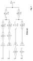
- the architecture of the dual-state power amplifier proposed by the present invention is shown at the Figs. 2 and 3 .
- This new architecture significantly improves the power amplifier efficiency at maximum and 6 dB backoff power levels by using two switches SW1 and SW2 connected at the ground ends GND of two additional parallel quarter-wavelength ⁇ /4 transmission line TL23 and TL24 having a characteristic impedance Zo. Additionally, the transmission lines TL31 and TL32 as well as TL43 and TL44 of the known power amplifier are now removed.
- the power amplifier of the present invention is shown in the two operation states: at Fig. 2 with the switches SW1 and SW2 closed, and at Fig. 3 with the switches SW1 and SW2 open.
- This power amplifier comprises
- the power amplifier further comprises a quarter-wavelength ⁇ /4 transmission line TL23 having a characteristic impedance Zo and being series connected with a first switch SW1 between the outlet of the second amplifier PA2 and the ground GND, as well as another quarter-wavelength ⁇ /4 transmission line TL24 having a characteristic impedance Zo and being series connected with a second switch SW2 between the junction point of the transmission lines TL13, TL14 and TL22 with the ground GND.
- the quarter-wavelength ⁇ /4 transmission lines TL11-TL14 and TL21-TL24 form together a 50 ⁇ matched transmission-line combiner or output power combiner of the power amplifier that operates under two modes depending upon the number of activated power amplifiers.
- the power amplifier is associated to a dual-mode input power divider coupling a general input RFin to the four inputs I1-I4.
- the input power divider comprises
- An impedance Z10 is further provided between a terminal A1 that is a junction point between the transmission lines TL61, TL51 and TL52, and a terminal A2 that is a junction point between the transmission lines TL62, TL53 and TL54.
- An impedance Z11 is also provided between the inputs I1 and I2, whilst another impedance Z12 is provided between the inputs I3 and I4.
- Both the power amplifier and the dual-mode input power divider form part of a dual-operating mode laterally diffused metal-oxide semiconductor LDMOS power amplifier.
- the switches SW1 and SW2 are turned on providing an open circuit conditions at the opposite input ends of these transmission lines TL23 and TL24, and all four power amplifiers PA1-PA4 are evenly delivering maximum power to the 50 ⁇ load.
- the power combining structure is symmetrical and each power amplifying path contains only two series quarter-wavelength transmission lines resulting in smaller losses compared to the above known combiner.
- switches are located between the ground and the ends of the parallel quarter-wavelength transmission lines at the opposite sides of the power combiner, they consume a very small amount of dc power.
- a bias control unit generally is necessary to turn on or off the transistors and the switches.
- the number of stages in all power amplifier stages may be different depending on the required output power and power gain, and the input and output impedances of each power amplifier are equal to Zo.
- switches can be used including the MEMS or pin-diode switches.
Landscapes
- Engineering & Computer Science (AREA)
- Power Engineering (AREA)
- Amplifiers (AREA)
- Microwave Amplifiers (AREA)
Abstract
Description
- The present invention relates to a dual-state power amplifier comprising
- a first amplifier having an inlet connected to a first input of said power amplifier and an outlet coupled to an output of said power amplifier via a first quarter-wavelength transmission line,
- a second amplifier having an inlet connected to a second input of said power amplifier and an outlet coupled to said output via a second quarter-wavelength transmission line,
- a third amplifier having an inlet coupled to a third input of said power amplifier and an outlet coupled to said output via a third quarter-wavelength transmission line,
- a fourth amplifier having an inlet coupled to a fourth input of said power amplifier and an outlet coupled to said output via a fourth quarter-wavelength transmission line,
- Such a dual-state power amplifier is already known in the art, e.g. from the article " Power Level-Dependent Dual-Operating Mode LDMOS Power Amplifier for CDMA Wireless Base-Station Applications" by Y. Chung, J. Jeong, Y. Wang, D. Ahn, and T. Itoh, published in the IEEE Transactions on Microwave Theory and Techniques, vol. MTT-53, pp. 739-746, Feb. 2005.00
- In most communication systems it is required that the power amplifier could operate with high efficiency and high linearity simultaneously. However, there is a tradeoff between efficiency and linearity with improvement in one coming at the expense of another. Besides, many wireless communications systems, such as Global System for Mobile communications/ Enhanced Data rates for GSM Evolution GSM/EDGE, code-division multiple-access CDMA2000 or wide-band code-division multiple-access W-CDMA, require that the power amplifier could deliver a wide range of output powers. As a result, being designed for the highest power level with maximum available efficiency, the power amplifiers in base stations tend to operate less efficiently at lower power levels consuming a lot of extra dc power.
- Therefore, it is a real challenge to design a base station power amplifier having high efficiency and high linearity not only at maximum output power but also at lower power levels typically ranging from -6 dBc and less without using of additional linearization schemes.
- The existing solution, disclosed in the above-mentioned article, is based on the possibility to use a combiner design technology for dual-state operation.
- In such a dual-state power amplifier shown in
Fig. 1 , the power amplifier consisting of a four-amplifier array (PA1-PA4) and a 50-Ω matched transmission-line combiner (TL11-TL14, TL21-TL22, TL31-TL32, TL43-TL44) operates under two modes depending upon the number of activated power amplifiers. - In a low-state operation, a power amplifier (PA1) is activated only, while all others (PA2-PA4) are switched off. It is assumed that, when power amplifier is switched off, its output impedance is nearly infinite (open circuit) and, due to the effect of the transmission lines with a quarter-wavelength length each, the three deactivated amplifiers are properly isolated from the activated amplifier.
- In a high-state operation, all four power amplifiers are evenly delivering maximum power to the 50-Q load.
- As a result, maximum efficiency is provided at maximum and 6-dB backoff output powers.
- However, in reality, at high frequencies the output impedance of a deactivated power amplifier is not an open circuit due to effect of the active device parasitic elements and output matching circuit. Also, additional losses occur due to the asymmetrical structure of the output combiner, and two quarter-wavelength transmission lines are necessary at the input so that the power can be added in phase at the output. As a result, the overall efficiency significantly degrades at both maximum and 6-dB output powers.
- An object of the present invention is to provide a dual-state power amplifier of the above known type but which provides high efficiency and high linearity for base station power amplifiers simultaneously at maximum and backoff output power levels.
- According to the invention, this object is achieved due to the fact that said power amplifier further comprises a seventh quarter-wavelength transmission line series connected with a first switch between the outlet of said second amplifier and the ground, and a eight quarter-wavelength transmission line series connected with a second switch between the junction point of said third, fourth and sixth transmission lines and the ground.
- The proposed architecture of the dual-state power amplifier significantly improves the power amplifier efficiency at maximum and 6-dB backoff power levels by using the two switches connected at the ground ends of the two additional parallel quarter-wavelength transmission lines.
- Moreover, since the switches are located between the ground and the ends of the parallel quarter-wavelength transmission lines at the opposite sides of the power combiner, they consume a very small amount of dc power.
- There is thus no need in using Digital PreDistortion DPD for performance linearization at backoff powers which is the case for inherently nonlinear Doherty power amplifier.
- Other characterizing embodiments of the present invention are that the four inputs of said power amplifier are coupled to outputs of a dual-mode input power divider comprising a plurality of quarter-wavelength transmission line, and that said power amplifier and said dual-mode input power divider form part of a dual-operating mode Laterally Diffused Metal-Oxide Semiconductor LDMOS structure.
- Such an amplifier is best suited for code-division multiple-access CDMA or wide-band code-division multiple-access W-CDMA wireless communication base-station applications.
- Further characterizing embodiments of the present dual-state power amplifier are mentioned in the appended claims.
- It is to be noticed that the term 'comprising', used in the claims, should not be interpreted as being restricted to the means listed thereafter. Thus, the scope of the expression 'a device comprising means A and B' should not be limited to devices consisting only of components A and B. It means that with respect to the present invention, the only relevant components of the device are A and B.
- Similarly, it is to be noticed that the term 'coupled', also used in the claims, should not be interpreted as being restricted to direct connections only. Thus, the scope of the expression 'a device A coupled to a device B' should not be limited to devices or systems wherein an output of device A is directly connected to an input of device B. It means that there exists a path between an output of A and an input of B which may be a path including other devices or means.
- The above and other objects and features of the invention will become more apparent and the invention itself will be best understood by referring to the following description of an embodiment taken in conjunction with the accompanying drawings wherein:
-
Fig. 1 represents a dual-state power amplifier as known from the prior art; -
Fig. 2 represents a dual-state power amplifier according to the invention in a first operating state (switches closed); -
Fig. 3 represents the dual-state power amplifier according to the invention in a second operating state (switches open); and -
Fig. 4 shows characteristics of the present dual-state power amplifier (solid line) with respect to those of a known power amplifier (dashed line). - The present invention relates to a dual-state power amplifier that preferably belongs to an amplifier structure consisting of four parallelly located single-stage LDMOS amplifier array PA1 to PA4, a dual-mode input power divider, and an output power combiner. The dual-operating mode Laterally Diffused Metal-Oxide Semiconductor LDMOS power amplifier is for instance used in code-division multiple-access wireless communication base-station applications.
- As mentioned above, a first design of such an amplifier structure is already known in the art and is shown at
Fig. 1 . The known power amplifier comprises four amplifiers PA1 to PA4 each coupling a distinct input I1 to I4 of the power amplifier to a common output RFout to which a 50 Ω load Zo is connected. It is to be noted that the dual-mode input power divider is not shown atFig. 1 but that four outputs thereof are connected to the four inputs I1-I4. - In the known power amplifier,
- a first amplifier PA1 has an inlet directly connected to the first input I1 and an outlet coupled to the output RFout via the series connection of a quarter-wavelength λ/4 transmission line TL31 having a characteristic impedance Zo, a quarter-wavelength λ/4 transmission line TL11 having a characteristic impedance

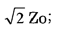
- a second amplifier PA2 has an inlet directly connected to the second input I2 and an outlet coupled to the output RFout via the series connection of a quarter-wavelength λ/4 transmission line TL32 having a characteristic impedance Zo, a quarter-wavelength λ/4 transmission line TL12 having a characteristic impedance

- a third amplifier PA3 has an inlet coupled to the third input I3 through a quarter-wavelength λ/4 transmission line TL43 having a characteristic impedance Zo, and an outlet coupled to the output RFout via the series connection of a quarter-wavelength λ/4 transmission line TL13 having a characteristic impedance
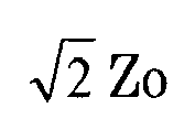

- a fourth amplifier PA4 has an inlet coupled to the fourth input I4 through a quarter-wavelength λ/4 transmission line TL44 having a characteristic impedance Zo, and an outlet coupled to the output RFout via the series connection of a quarter-wavelength λ/4 transmission line TL14 having a characteristic impedance

- The quarter-wavelength λ/4 transmission lines TL11-TL14, TL21-TL22 and TL31-TL32 form together a 50Ω matched transmission-line combiner or output power combiner of the power amplifier that operates under two modes depending upon the number of activated power amplifiers.
- In a low-state operation, the power amplifier PA1 is activated only, while all other amplifiers PA2-PA4 are switched off. It is assumed that, when power amplifier is switched off, its output impedance is nearly infinite (open circuit) and, due to the effect of the transmission lines with a quarter-wavelength length each, the three deactivated amplifiers are properly isolated from the activated amplifier.
- In a high-state operation, all four power amplifiers PA1-PA4 are evenly delivering maximum power to the 50 Ω load Zo.
- The architecture of the dual-state power amplifier proposed by the present invention is shown at the
Figs. 2 and3 . This new architecture significantly improves the power amplifier efficiency at maximum and 6 dB backoff power levels by using two switches SW1 and SW2 connected at the ground ends GND of two additional parallel quarter-wavelength λ/4 transmission line TL23 and TL24 having a characteristic impedance Zo. Additionally, the transmission lines TL31 and TL32 as well as TL43 and TL44 of the known power amplifier are now removed. - The power amplifier of the present invention is shown in the two operation states: at
Fig. 2 with the switches SW1 and SW2 closed, and atFig. 3 with the switches SW1 and SW2 open. - This power amplifier comprises
- a first amplifier PA1 having an inlet directly connected to the first input I1 and an outlet coupled to the output RFout via the series connection of a quarter-wavelength λ/4 transmission line TL11 having a characteristic impedance


- a second amplifier PA2 having an inlet directly connected to the second input I2 and an outlet coupled to the output RFout via the series connection of a quarter-wavelength λ/4 transmission line TL12 having a characteristic impedance

- a third amplifier PA3 having an inlet directly connected to the third input I3 and an outlet coupled to the output RFout via the series connection of a quarter-wavelength λ/4 transmission line TL13 having a characteristic impedance


- a fourth amplifier PA4 having an inlet coupled to the fourth input I4 and an outlet coupled to the output RFout via the series connection of a quarter-wavelength λ/4 transmission line TL14 having a characteristic impedance

- The power amplifier further comprises a quarter-wavelength λ/4 transmission line TL23 having a characteristic impedance Zo and being series connected with a first switch SW1 between the outlet of the second amplifier PA2 and the ground GND, as well as another quarter-wavelength λ/4 transmission line TL24 having a characteristic impedance Zo and being series connected with a second switch SW2 between the junction point of the transmission lines TL13, TL14 and TL22 with the ground GND.
- The quarter-wavelength λ/4 transmission lines TL11-TL14 and TL21-TL24 form together a 50Ω matched transmission-line combiner or output power combiner of the power amplifier that operates under two modes depending upon the number of activated power amplifiers.
- As already mentioned, the power amplifier is associated to a dual-mode input power divider coupling a general input RFin to the four inputs I1-I4.
- The input power divider comprises
- the series connection of a quarter-wavelength λ/4 transmission line TL61 having a characteristic impedance


- the series connection of the transmission line TL61 with a quarter-wavelength λ/4 transmission line TL52 having a characteristic impedance

- the series connection of a quarter-wavelength λ/4 transmission line TL62 having a characteristic impedance


- the series connection of the transmission line TL62 with a quarter-wavelength λ/4 transmission line TL54 having a characteristic impedance

- An impedance Z10 is further provided between a terminal A1 that is a junction point between the transmission lines TL61, TL51 and TL52, and a terminal A2 that is a junction point between the transmission lines TL62, TL53 and TL54.
- An impedance Z11 is also provided between the inputs I1 and I2, whilst another impedance Z12 is provided between the inputs I3 and I4.
- Both the power amplifier and the dual-mode input power divider form part of a dual-operating mode laterally diffused metal-oxide semiconductor LDMOS power amplifier.
- As shown at
Fig. 2 , in a high-power mode when all four power amplifiers PA1-PA4 are activated, the switches SW1 and SW2 are turned on providing an open circuit conditions at the opposite input ends of these transmission lines TL23 and TL24, and all four power amplifiers PA1-PA4 are evenly delivering maximum power to the 50 Ω load. In this case, the power combining structure is symmetrical and each power amplifying path contains only two series quarter-wavelength transmission lines resulting in smaller losses compared to the above known combiner. - In a low-state mode when the power amplifier PA1 is activated only, as shown at
Fig. 3 , the switches SW1 and SW2 are turned off providing a short circuit conditions at the input ends of these quarter-wavelength transmission lines, resulting in a complete isolation of the deactivated power amplifiers PA2-PA4 from the activated one PA1. - Consequently, the two peak high efficiencies can be achieved at maximum and 6 dB backoff power levels, as shown in
Fig. 4 (dashed line corresponds to the above known power amplifier represented atFig. 1 ), and these efficiencies will be significantly higher than that of for this known dual-state power amplifier. - Moreover, since the switches are located between the ground and the ends of the parallel quarter-wavelength transmission lines at the opposite sides of the power combiner, they consume a very small amount of dc power.
- It is to be noted that a bias control unit generally is necessary to turn on or off the transistors and the switches.
- It is also to be noted that the number of stages in all power amplifier stages may be different depending on the required output power and power gain, and the input and output impedances of each power amplifier are equal to Zo.
- It is finally to be noted that any type of switches can be used including the MEMS or pin-diode switches.
- A final remark is that embodiments of the present invention are described above in terms of functional blocks. From the functional description of these blocks, given above, it will be apparent for a person skilled in the art of designing electronic devices how embodiments of these blocks can be manufactured with well-known electronic components. A detailed architecture of the contents of the functional blocks hence is not given.
- While the principles of the invention have been described above in connection with specific apparatus, it is to be clearly understood that this description is merely made by way of example and not as a limitation on the scope of the invention, as defined in the appended claims.
Claims (7)
- A dual-state power amplifier comprising
a first amplifier (PA1) having an inlet connected to a first input (I1) of said power amplifier and an outlet coupled to an output (RFout) of said power amplifier via a first quarter-wavelength transmission line (TL11),
a second amplifier (PA2) having an inlet connected to a second input (I2) of said power amplifier and an outlet coupled to said output (RFout) via a second quarter-wavelength transmission line (TL12),
a third amplifier (PA3) having an inlet coupled to a third input (I3) of said power amplifier and an outlet coupled to said output (RFout) via a third quarter-wavelength transmission line (TL13),
a fourth amplifier (PA4) having an inlet coupled to a fourth input (I4) of said power amplifier and an outlet coupled to said output (RFout) via a fourth quarter-wavelength transmission line (TL14),
said first (TL11) and second (TL12) transmission line being connected in common to said output (RFout) via a fifth quarter-wavelength transmission line (TL21), whilst said third (TL13) and fourth (TL14) transmission lines being connected in common to said output (RFout) via a sixth quarter-wavelength transmission line (TL22),
characterized in that said power amplifier further comprises a seventh quarter-wavelength transmission line (TL23) series connected with a first switch (SW1) between the outlet of said second amplifier (PA2) and the ground (GND),
and an eight quarter-wavelength transmission line (TL24) series connected with a second switch (SW2) between the junction point of said third (TL13), fourth (TL14) and sixth (TL22) transmission lines and the ground (GND). - The power amplifier according to claim 1, characterized in that said power amplifier is adapted to operate either with only said first amplifier (PA1) or with all said four amplifiers (PA1-PA4).
- The power amplifier according to claim 1, characterized in that said four inputs (I1-I4) of said power amplifier are coupled to outputs of a dual-mode input power divider comprising a plurality of quarter-wavelength transmission line (TL51-TL54, TL61, TL62).
- The power amplifier according to claim 3, characterized in that said power amplifier and said dual-mode input power divider form part of a dual-operating mode laterally diffused metal-oxide semiconductor LDMOS structure.
- The power amplifier according to claim 1, characterized in that said first (SW1) and second (SW2) switches are designed according to the MEMS technology.
- The power amplifier according to claim 1, characterized in that said first (SW1) and second (SW2) switches are pin-diode switches.
- The power amplifier according to claim 1, characterized in that said output (RFout) is connected to a 50 Ω load (Zo).
Priority Applications (2)
| Application Number | Priority Date | Filing Date | Title |
|---|---|---|---|
| EP08290905A EP2169825B1 (en) | 2008-09-24 | 2008-09-24 | High-efficiency dual-state power amplifier |
| AT08290905T ATE546880T1 (en) | 2008-09-24 | 2008-09-24 | HIGH POWER DUAL POWER AMPLIFIER |
Applications Claiming Priority (1)
| Application Number | Priority Date | Filing Date | Title |
|---|---|---|---|
| EP08290905A EP2169825B1 (en) | 2008-09-24 | 2008-09-24 | High-efficiency dual-state power amplifier |
Publications (2)
| Publication Number | Publication Date |
|---|---|
| EP2169825A1 true EP2169825A1 (en) | 2010-03-31 |
| EP2169825B1 EP2169825B1 (en) | 2012-02-22 |
Family
ID=40111093
Family Applications (1)
| Application Number | Title | Priority Date | Filing Date |
|---|---|---|---|
| EP08290905A Not-in-force EP2169825B1 (en) | 2008-09-24 | 2008-09-24 | High-efficiency dual-state power amplifier |
Country Status (2)
| Country | Link |
|---|---|
| EP (1) | EP2169825B1 (en) |
| AT (1) | ATE546880T1 (en) |
Cited By (1)
| Publication number | Priority date | Publication date | Assignee | Title |
|---|---|---|---|---|
| US20240125876A1 (en) * | 2022-10-14 | 2024-04-18 | Bruker France Sas | Microwave power amplifier arrangement for a pulsed epr system |
Citations (4)
| Publication number | Priority date | Publication date | Assignee | Title |
|---|---|---|---|---|
| US5025225A (en) * | 1989-12-15 | 1991-06-18 | Raytheon Company | Amplifier having substantially constant D.C. to r.f. conversion efficiency |
| US6097266A (en) * | 1998-08-14 | 2000-08-01 | Lucent Technologies Inc | Intelligent RF combiner |
| WO2001063756A1 (en) * | 2000-02-24 | 2001-08-30 | Wireless Systems International Limited | A signal combiner, a signal splitter and a circuit using a combiner and a splitter |
| US20080136554A1 (en) * | 2004-11-19 | 2008-06-12 | He Pinghua | System, microwave switch and method for hot standby of radio frequency power amplifier |
-
2008
- 2008-09-24 AT AT08290905T patent/ATE546880T1/en active
- 2008-09-24 EP EP08290905A patent/EP2169825B1/en not_active Not-in-force
Patent Citations (4)
| Publication number | Priority date | Publication date | Assignee | Title |
|---|---|---|---|---|
| US5025225A (en) * | 1989-12-15 | 1991-06-18 | Raytheon Company | Amplifier having substantially constant D.C. to r.f. conversion efficiency |
| US6097266A (en) * | 1998-08-14 | 2000-08-01 | Lucent Technologies Inc | Intelligent RF combiner |
| WO2001063756A1 (en) * | 2000-02-24 | 2001-08-30 | Wireless Systems International Limited | A signal combiner, a signal splitter and a circuit using a combiner and a splitter |
| US20080136554A1 (en) * | 2004-11-19 | 2008-06-12 | He Pinghua | System, microwave switch and method for hot standby of radio frequency power amplifier |
Non-Patent Citations (3)
| Title |
|---|
| CHUNG ET AL.: "Power Level-Dependent Dual-Operating Mode LDMOS Power Amplifier for CDMA Wireless Base-Station Applications", IEEE TRANSACTIONS ON MICROWAVE THEORY AND TECHNIQUES, vol. MTT-53, February 2005 (2005-02-01), pages 739 - 746, XP011126921, DOI: doi:10.1109/TMTT.2004.841220 |
| CYNTHIA Y HANG ET AL: "A High Efficiency Power Amplifier System for CDMA", EUROPEAN MICROWAVE CONFERENCE, 2002. 32ND, IEEE, PISCATAWAY, NJ, USA, 1 October 2002 (2002-10-01), pages 1 - 3, XP031068174 * |
| YOUNKYU CHUNG ET AL: "Efficiency-enhancing technique: LDMOS power amplifier using dual-mode operation design approach", MICROWAVE SYMPOSIUM DIGEST, 2004 IEEE MTT-S INTERNATIONAL FORT WORTH, TX, USA JUNE 6-11, 2004, PISCATAWAY, NJ, USA,IEEE, vol. 2, 6 June 2004 (2004-06-06), pages 859 - 862, XP010728255, ISBN: 978-0-7803-8331-9 * |
Cited By (2)
| Publication number | Priority date | Publication date | Assignee | Title |
|---|---|---|---|---|
| US20240125876A1 (en) * | 2022-10-14 | 2024-04-18 | Bruker France Sas | Microwave power amplifier arrangement for a pulsed epr system |
| US12392848B2 (en) * | 2022-10-14 | 2025-08-19 | Bruker France Sas | Microwave power amplifier arrangement for a pulsed EPR system |
Also Published As
| Publication number | Publication date |
|---|---|
| EP2169825B1 (en) | 2012-02-22 |
| ATE546880T1 (en) | 2012-03-15 |
Similar Documents
| Publication | Publication Date | Title |
|---|---|---|
| US10763798B2 (en) | Variable impedance match and variable harmonic terminations for different modes and frequency bands | |
| Chen et al. | A monolithically integrated single-input load-modulated balanced amplifier with enhanced efficiency at power back-off | |
| US6085074A (en) | Apparatus and method for amplifying an amplitude-varying signal | |
| US10749478B2 (en) | Amplifier arrangement | |
| US7345537B2 (en) | Linear power amplifier with multiple output power levels | |
| Kim et al. | A multiband reconfigurable power amplifier for UMTS handset applications | |
| US8095092B2 (en) | Power efficient transmitter with high dynamic range | |
| JP5417064B2 (en) | High frequency power amplifier | |
| EP2169823B1 (en) | Combined multi-path high-efficiency power amplifier | |
| CN110999073A (en) | Broadband, High Efficiency, Unmodulated Power Amplifier Architecture | |
| JP2001223539A (en) | Linear power amplifier based on active feedforward type predistortion | |
| WO2013015778A1 (en) | Actively tuned circuit having parallel carrier and peaking paths | |
| JP2008125044A (en) | amplifier | |
| EP2169825B1 (en) | High-efficiency dual-state power amplifier | |
| Huang et al. | A 35–100GHz continuous mode coupler balun Doherty power amplifier with differential complex neutralization in 250nm InP | |
| CN111342780A (en) | Linearity enhancement for high power amplifiers | |
| Wood et al. | A high power, high efficiency UMTS amplifier using a novel Doherty configuration | |
| Zeng et al. | Design of a High-Efficiency Outphasing Power Amplifier With Enhancing Back-Off Range for 5G Applications | |
| WO2003065598A1 (en) | Power amplification apparatus of portable terminal | |
| US8860506B2 (en) | Amplifying apparatus | |
| US12620948B2 (en) | RF amplifier circuit arrangement and electronic device | |
| US12620949B2 (en) | Amplifier circuit arrangement and electronic device | |
| US20230370028A1 (en) | RF amplifier circuit arrangement and electronic device | |
| Noh et al. | Linearized high efficient HBT power amplifier module for L-band application | |
| US6522196B1 (en) | System and method for improving input return loss in RF amplifiers |
Legal Events
| Date | Code | Title | Description |
|---|---|---|---|
| PUAI | Public reference made under article 153(3) epc to a published international application that has entered the european phase |
Free format text: ORIGINAL CODE: 0009012 |
|
| AK | Designated contracting states |
Kind code of ref document: A1 Designated state(s): AT BE BG CH CY CZ DE DK EE ES FI FR GB GR HR HU IE IS IT LI LT LU LV MC MT NL NO PL PT RO SE SI SK TR |
|
| AX | Request for extension of the european patent |
Extension state: AL BA MK RS |
|
| 17P | Request for examination filed |
Effective date: 20100930 |
|
| AKX | Designation fees paid |
Designated state(s): AT BE BG CH CY CZ DE DK EE ES FI FR GB GR HR HU IE IS IT LI LT LU LV MC MT NL NO PL PT RO SE SI SK TR |
|
| GRAP | Despatch of communication of intention to grant a patent |
Free format text: ORIGINAL CODE: EPIDOSNIGR1 |
|
| RTI1 | Title (correction) |
Free format text: HIGH-EFFICIENCY DUAL-STATE POWER AMPLIFIER |
|
| GRAS | Grant fee paid |
Free format text: ORIGINAL CODE: EPIDOSNIGR3 |
|
| GRAA | (expected) grant |
Free format text: ORIGINAL CODE: 0009210 |
|
| AK | Designated contracting states |
Kind code of ref document: B1 Designated state(s): AT BE BG CH CY CZ DE DK EE ES FI FR GB GR HR HU IE IS IT LI LT LU LV MC MT NL NO PL PT RO SE SI SK TR |
|
| RAP1 | Party data changed (applicant data changed or rights of an application transferred) |
Owner name: ALCATEL LUCENT |
|
| REG | Reference to a national code |
Ref country code: GB Ref legal event code: FG4D |
|
| REG | Reference to a national code |
Ref country code: CH Ref legal event code: EP |
|
| REG | Reference to a national code |
Ref country code: AT Ref legal event code: REF Ref document number: 546880 Country of ref document: AT Kind code of ref document: T Effective date: 20120315 |
|
| REG | Reference to a national code |
Ref country code: IE Ref legal event code: FG4D |
|
| REG | Reference to a national code |
Ref country code: DE Ref legal event code: R096 Ref document number: 602008013565 Country of ref document: DE Effective date: 20120419 |
|
| REG | Reference to a national code |
Ref country code: NL Ref legal event code: VDEP Effective date: 20120222 |
|
| LTIE | Lt: invalidation of european patent or patent extension |
Effective date: 20120222 |
|
| PG25 | Lapsed in a contracting state [announced via postgrant information from national office to epo] |
Ref country code: NL Free format text: LAPSE BECAUSE OF FAILURE TO SUBMIT A TRANSLATION OF THE DESCRIPTION OR TO PAY THE FEE WITHIN THE PRESCRIBED TIME-LIMIT Effective date: 20120222 Ref country code: HR Free format text: LAPSE BECAUSE OF FAILURE TO SUBMIT A TRANSLATION OF THE DESCRIPTION OR TO PAY THE FEE WITHIN THE PRESCRIBED TIME-LIMIT Effective date: 20120222 Ref country code: NO Free format text: LAPSE BECAUSE OF FAILURE TO SUBMIT A TRANSLATION OF THE DESCRIPTION OR TO PAY THE FEE WITHIN THE PRESCRIBED TIME-LIMIT Effective date: 20120522 Ref country code: LT Free format text: LAPSE BECAUSE OF FAILURE TO SUBMIT A TRANSLATION OF THE DESCRIPTION OR TO PAY THE FEE WITHIN THE PRESCRIBED TIME-LIMIT Effective date: 20120222 Ref country code: IS Free format text: LAPSE BECAUSE OF FAILURE TO SUBMIT A TRANSLATION OF THE DESCRIPTION OR TO PAY THE FEE WITHIN THE PRESCRIBED TIME-LIMIT Effective date: 20120622 |
|
| PG25 | Lapsed in a contracting state [announced via postgrant information from national office to epo] |
Ref country code: LV Free format text: LAPSE BECAUSE OF FAILURE TO SUBMIT A TRANSLATION OF THE DESCRIPTION OR TO PAY THE FEE WITHIN THE PRESCRIBED TIME-LIMIT Effective date: 20120222 Ref country code: BE Free format text: LAPSE BECAUSE OF FAILURE TO SUBMIT A TRANSLATION OF THE DESCRIPTION OR TO PAY THE FEE WITHIN THE PRESCRIBED TIME-LIMIT Effective date: 20120222 Ref country code: FI Free format text: LAPSE BECAUSE OF FAILURE TO SUBMIT A TRANSLATION OF THE DESCRIPTION OR TO PAY THE FEE WITHIN THE PRESCRIBED TIME-LIMIT Effective date: 20120222 Ref country code: PT Free format text: LAPSE BECAUSE OF FAILURE TO SUBMIT A TRANSLATION OF THE DESCRIPTION OR TO PAY THE FEE WITHIN THE PRESCRIBED TIME-LIMIT Effective date: 20120622 Ref country code: GR Free format text: LAPSE BECAUSE OF FAILURE TO SUBMIT A TRANSLATION OF THE DESCRIPTION OR TO PAY THE FEE WITHIN THE PRESCRIBED TIME-LIMIT Effective date: 20120523 |
|
| REG | Reference to a national code |
Ref country code: AT Ref legal event code: MK05 Ref document number: 546880 Country of ref document: AT Kind code of ref document: T Effective date: 20120222 |
|
| PG25 | Lapsed in a contracting state [announced via postgrant information from national office to epo] |
Ref country code: CY Free format text: LAPSE BECAUSE OF FAILURE TO SUBMIT A TRANSLATION OF THE DESCRIPTION OR TO PAY THE FEE WITHIN THE PRESCRIBED TIME-LIMIT Effective date: 20120222 |
|
| PG25 | Lapsed in a contracting state [announced via postgrant information from national office to epo] |
Ref country code: SE Free format text: LAPSE BECAUSE OF FAILURE TO SUBMIT A TRANSLATION OF THE DESCRIPTION OR TO PAY THE FEE WITHIN THE PRESCRIBED TIME-LIMIT Effective date: 20120222 Ref country code: RO Free format text: LAPSE BECAUSE OF FAILURE TO SUBMIT A TRANSLATION OF THE DESCRIPTION OR TO PAY THE FEE WITHIN THE PRESCRIBED TIME-LIMIT Effective date: 20120222 Ref country code: EE Free format text: LAPSE BECAUSE OF FAILURE TO SUBMIT A TRANSLATION OF THE DESCRIPTION OR TO PAY THE FEE WITHIN THE PRESCRIBED TIME-LIMIT Effective date: 20120222 Ref country code: CZ Free format text: LAPSE BECAUSE OF FAILURE TO SUBMIT A TRANSLATION OF THE DESCRIPTION OR TO PAY THE FEE WITHIN THE PRESCRIBED TIME-LIMIT Effective date: 20120222 Ref country code: SI Free format text: LAPSE BECAUSE OF FAILURE TO SUBMIT A TRANSLATION OF THE DESCRIPTION OR TO PAY THE FEE WITHIN THE PRESCRIBED TIME-LIMIT Effective date: 20120222 Ref country code: DK Free format text: LAPSE BECAUSE OF FAILURE TO SUBMIT A TRANSLATION OF THE DESCRIPTION OR TO PAY THE FEE WITHIN THE PRESCRIBED TIME-LIMIT Effective date: 20120222 Ref country code: PL Free format text: LAPSE BECAUSE OF FAILURE TO SUBMIT A TRANSLATION OF THE DESCRIPTION OR TO PAY THE FEE WITHIN THE PRESCRIBED TIME-LIMIT Effective date: 20120222 |
|
| PG25 | Lapsed in a contracting state [announced via postgrant information from national office to epo] |
Ref country code: IT Free format text: LAPSE BECAUSE OF FAILURE TO SUBMIT A TRANSLATION OF THE DESCRIPTION OR TO PAY THE FEE WITHIN THE PRESCRIBED TIME-LIMIT Effective date: 20120222 Ref country code: SK Free format text: LAPSE BECAUSE OF FAILURE TO SUBMIT A TRANSLATION OF THE DESCRIPTION OR TO PAY THE FEE WITHIN THE PRESCRIBED TIME-LIMIT Effective date: 20120222 |
|
| PLBE | No opposition filed within time limit |
Free format text: ORIGINAL CODE: 0009261 |
|
| STAA | Information on the status of an ep patent application or granted ep patent |
Free format text: STATUS: NO OPPOSITION FILED WITHIN TIME LIMIT |
|
| 26N | No opposition filed |
Effective date: 20121123 |
|
| PG25 | Lapsed in a contracting state [announced via postgrant information from national office to epo] |
Ref country code: AT Free format text: LAPSE BECAUSE OF FAILURE TO SUBMIT A TRANSLATION OF THE DESCRIPTION OR TO PAY THE FEE WITHIN THE PRESCRIBED TIME-LIMIT Effective date: 20120222 |
|
| REG | Reference to a national code |
Ref country code: DE Ref legal event code: R097 Ref document number: 602008013565 Country of ref document: DE Effective date: 20121123 |
|
| PG25 | Lapsed in a contracting state [announced via postgrant information from national office to epo] |
Ref country code: ES Free format text: LAPSE BECAUSE OF FAILURE TO SUBMIT A TRANSLATION OF THE DESCRIPTION OR TO PAY THE FEE WITHIN THE PRESCRIBED TIME-LIMIT Effective date: 20120602 Ref country code: MC Free format text: LAPSE BECAUSE OF NON-PAYMENT OF DUE FEES Effective date: 20120930 |
|
| REG | Reference to a national code |
Ref country code: CH Ref legal event code: PL |
|
| REG | Reference to a national code |
Ref country code: IE Ref legal event code: MM4A |
|
| PG25 | Lapsed in a contracting state [announced via postgrant information from national office to epo] |
Ref country code: CH Free format text: LAPSE BECAUSE OF NON-PAYMENT OF DUE FEES Effective date: 20120930 Ref country code: IE Free format text: LAPSE BECAUSE OF NON-PAYMENT OF DUE FEES Effective date: 20120924 Ref country code: BG Free format text: LAPSE BECAUSE OF FAILURE TO SUBMIT A TRANSLATION OF THE DESCRIPTION OR TO PAY THE FEE WITHIN THE PRESCRIBED TIME-LIMIT Effective date: 20120522 Ref country code: LI Free format text: LAPSE BECAUSE OF NON-PAYMENT OF DUE FEES Effective date: 20120930 |
|
| REG | Reference to a national code |
Ref country code: FR Ref legal event code: GC Effective date: 20131018 |
|
| PG25 | Lapsed in a contracting state [announced via postgrant information from national office to epo] |
Ref country code: MT Free format text: LAPSE BECAUSE OF FAILURE TO SUBMIT A TRANSLATION OF THE DESCRIPTION OR TO PAY THE FEE WITHIN THE PRESCRIBED TIME-LIMIT Effective date: 20120222 |
|
| PG25 | Lapsed in a contracting state [announced via postgrant information from national office to epo] |
Ref country code: TR Free format text: LAPSE BECAUSE OF FAILURE TO SUBMIT A TRANSLATION OF THE DESCRIPTION OR TO PAY THE FEE WITHIN THE PRESCRIBED TIME-LIMIT Effective date: 20120222 |
|
| PG25 | Lapsed in a contracting state [announced via postgrant information from national office to epo] |
Ref country code: LU Free format text: LAPSE BECAUSE OF NON-PAYMENT OF DUE FEES Effective date: 20120924 |
|
| PG25 | Lapsed in a contracting state [announced via postgrant information from national office to epo] |
Ref country code: HU Free format text: LAPSE BECAUSE OF FAILURE TO SUBMIT A TRANSLATION OF THE DESCRIPTION OR TO PAY THE FEE WITHIN THE PRESCRIBED TIME-LIMIT Effective date: 20080924 |
|
| REG | Reference to a national code |
Ref country code: FR Ref legal event code: RG Effective date: 20141016 |
|
| REG | Reference to a national code |
Ref country code: FR Ref legal event code: PLFP Year of fee payment: 8 |
|
| REG | Reference to a national code |
Ref country code: FR Ref legal event code: PLFP Year of fee payment: 9 |
|
| REG | Reference to a national code |
Ref country code: FR Ref legal event code: PLFP Year of fee payment: 10 |
|
| PGFP | Annual fee paid to national office [announced via postgrant information from national office to epo] |
Ref country code: GB Payment date: 20180327 Year of fee payment: 10 |
|
| PGFP | Annual fee paid to national office [announced via postgrant information from national office to epo] |
Ref country code: FR Payment date: 20180329 Year of fee payment: 10 |
|
| PGFP | Annual fee paid to national office [announced via postgrant information from national office to epo] |
Ref country code: DE Payment date: 20180328 Year of fee payment: 10 |
|
| REG | Reference to a national code |
Ref country code: DE Ref legal event code: R119 Ref document number: 602008013565 Country of ref document: DE |
|
| GBPC | Gb: european patent ceased through non-payment of renewal fee |
Effective date: 20180924 |
|
| PG25 | Lapsed in a contracting state [announced via postgrant information from national office to epo] |
Ref country code: DE Free format text: LAPSE BECAUSE OF NON-PAYMENT OF DUE FEES Effective date: 20190402 |
|
| PG25 | Lapsed in a contracting state [announced via postgrant information from national office to epo] |
Ref country code: FR Free format text: LAPSE BECAUSE OF NON-PAYMENT OF DUE FEES Effective date: 20180930 |
|
| PG25 | Lapsed in a contracting state [announced via postgrant information from national office to epo] |
Ref country code: GB Free format text: LAPSE BECAUSE OF NON-PAYMENT OF DUE FEES Effective date: 20180924 |
|
| REG | Reference to a national code |
Ref country code: DE Ref legal event code: R081 Ref document number: 602008013565 Country of ref document: DE Owner name: WSOU INVESTMENTS, LLC, LOS ANGELES, US Free format text: FORMER OWNER: ALCATEL LUCENT, PARIS, FR Ref country code: DE Ref legal event code: R082 Ref document number: 602008013565 Country of ref document: DE Representative=s name: BARKHOFF REIMANN VOSSIUS, DE |
|
| REG | Reference to a national code |
Ref country code: GB Ref legal event code: 732E Free format text: REGISTERED BETWEEN 20200924 AND 20200930 |