EP2169457A1 - Display manufacturing method - Google Patents
Display manufacturing method Download PDFInfo
- Publication number
- EP2169457A1 EP2169457A1 EP08778207A EP08778207A EP2169457A1 EP 2169457 A1 EP2169457 A1 EP 2169457A1 EP 08778207 A EP08778207 A EP 08778207A EP 08778207 A EP08778207 A EP 08778207A EP 2169457 A1 EP2169457 A1 EP 2169457A1
- Authority
- EP
- European Patent Office
- Prior art keywords
- resin composition
- protective part
- display part
- display device
- display
- Prior art date
- Legal status (The legal status is an assumption and is not a legal conclusion. Google has not performed a legal analysis and makes no representation as to the accuracy of the status listed.)
- Granted
Links
Images



Classifications
-
- G—PHYSICS
- G02—OPTICS
- G02F—OPTICAL DEVICES OR ARRANGEMENTS FOR THE CONTROL OF LIGHT BY MODIFICATION OF THE OPTICAL PROPERTIES OF THE MEDIA OF THE ELEMENTS INVOLVED THEREIN; NON-LINEAR OPTICS; FREQUENCY-CHANGING OF LIGHT; OPTICAL LOGIC ELEMENTS; OPTICAL ANALOGUE/DIGITAL CONVERTERS
- G02F1/00—Devices or arrangements for the control of the intensity, colour, phase, polarisation or direction of light arriving from an independent light source, e.g. switching, gating or modulating; Non-linear optics
- G02F1/01—Devices or arrangements for the control of the intensity, colour, phase, polarisation or direction of light arriving from an independent light source, e.g. switching, gating or modulating; Non-linear optics for the control of the intensity, phase, polarisation or colour
- G02F1/13—Devices or arrangements for the control of the intensity, colour, phase, polarisation or direction of light arriving from an independent light source, e.g. switching, gating or modulating; Non-linear optics for the control of the intensity, phase, polarisation or colour based on liquid crystals, e.g. single liquid crystal display cells
- G02F1/133—Constructional arrangements; Operation of liquid crystal cells; Circuit arrangements
- G02F1/1333—Constructional arrangements; Manufacturing methods
- G02F1/133308—Support structures for LCD panels, e.g. frames or bezels
-
- G—PHYSICS
- G02—OPTICS
- G02F—OPTICAL DEVICES OR ARRANGEMENTS FOR THE CONTROL OF LIGHT BY MODIFICATION OF THE OPTICAL PROPERTIES OF THE MEDIA OF THE ELEMENTS INVOLVED THEREIN; NON-LINEAR OPTICS; FREQUENCY-CHANGING OF LIGHT; OPTICAL LOGIC ELEMENTS; OPTICAL ANALOGUE/DIGITAL CONVERTERS
- G02F1/00—Devices or arrangements for the control of the intensity, colour, phase, polarisation or direction of light arriving from an independent light source, e.g. switching, gating or modulating; Non-linear optics
- G02F1/01—Devices or arrangements for the control of the intensity, colour, phase, polarisation or direction of light arriving from an independent light source, e.g. switching, gating or modulating; Non-linear optics for the control of the intensity, phase, polarisation or colour
- G02F1/13—Devices or arrangements for the control of the intensity, colour, phase, polarisation or direction of light arriving from an independent light source, e.g. switching, gating or modulating; Non-linear optics for the control of the intensity, phase, polarisation or colour based on liquid crystals, e.g. single liquid crystal display cells
- G02F1/133—Constructional arrangements; Operation of liquid crystal cells; Circuit arrangements
- G02F1/1333—Constructional arrangements; Manufacturing methods
-
- G—PHYSICS
- G02—OPTICS
- G02F—OPTICAL DEVICES OR ARRANGEMENTS FOR THE CONTROL OF LIGHT BY MODIFICATION OF THE OPTICAL PROPERTIES OF THE MEDIA OF THE ELEMENTS INVOLVED THEREIN; NON-LINEAR OPTICS; FREQUENCY-CHANGING OF LIGHT; OPTICAL LOGIC ELEMENTS; OPTICAL ANALOGUE/DIGITAL CONVERTERS
- G02F1/00—Devices or arrangements for the control of the intensity, colour, phase, polarisation or direction of light arriving from an independent light source, e.g. switching, gating or modulating; Non-linear optics
- G02F1/01—Devices or arrangements for the control of the intensity, colour, phase, polarisation or direction of light arriving from an independent light source, e.g. switching, gating or modulating; Non-linear optics for the control of the intensity, phase, polarisation or colour
- G02F1/13—Devices or arrangements for the control of the intensity, colour, phase, polarisation or direction of light arriving from an independent light source, e.g. switching, gating or modulating; Non-linear optics for the control of the intensity, phase, polarisation or colour based on liquid crystals, e.g. single liquid crystal display cells
- G02F1/133—Constructional arrangements; Operation of liquid crystal cells; Circuit arrangements
- G02F1/1333—Constructional arrangements; Manufacturing methods
- G02F1/133308—Support structures for LCD panels, e.g. frames or bezels
- G02F1/133311—Environmental protection, e.g. against dust or humidity
-
- G—PHYSICS
- G02—OPTICS
- G02F—OPTICAL DEVICES OR ARRANGEMENTS FOR THE CONTROL OF LIGHT BY MODIFICATION OF THE OPTICAL PROPERTIES OF THE MEDIA OF THE ELEMENTS INVOLVED THEREIN; NON-LINEAR OPTICS; FREQUENCY-CHANGING OF LIGHT; OPTICAL LOGIC ELEMENTS; OPTICAL ANALOGUE/DIGITAL CONVERTERS
- G02F1/00—Devices or arrangements for the control of the intensity, colour, phase, polarisation or direction of light arriving from an independent light source, e.g. switching, gating or modulating; Non-linear optics
- G02F1/01—Devices or arrangements for the control of the intensity, colour, phase, polarisation or direction of light arriving from an independent light source, e.g. switching, gating or modulating; Non-linear optics for the control of the intensity, phase, polarisation or colour
- G02F1/13—Devices or arrangements for the control of the intensity, colour, phase, polarisation or direction of light arriving from an independent light source, e.g. switching, gating or modulating; Non-linear optics for the control of the intensity, phase, polarisation or colour based on liquid crystals, e.g. single liquid crystal display cells
- G02F1/133—Constructional arrangements; Operation of liquid crystal cells; Circuit arrangements
- G02F1/1333—Constructional arrangements; Manufacturing methods
- G02F1/133308—Support structures for LCD panels, e.g. frames or bezels
- G02F1/133331—Cover glasses
-
- G—PHYSICS
- G02—OPTICS
- G02F—OPTICAL DEVICES OR ARRANGEMENTS FOR THE CONTROL OF LIGHT BY MODIFICATION OF THE OPTICAL PROPERTIES OF THE MEDIA OF THE ELEMENTS INVOLVED THEREIN; NON-LINEAR OPTICS; FREQUENCY-CHANGING OF LIGHT; OPTICAL LOGIC ELEMENTS; OPTICAL ANALOGUE/DIGITAL CONVERTERS
- G02F2202/00—Materials and properties
- G02F2202/02—Materials and properties organic material
- G02F2202/022—Materials and properties organic material polymeric
- G02F2202/023—Materials and properties organic material polymeric curable
-
- G—PHYSICS
- G02—OPTICS
- G02F—OPTICAL DEVICES OR ARRANGEMENTS FOR THE CONTROL OF LIGHT BY MODIFICATION OF THE OPTICAL PROPERTIES OF THE MEDIA OF THE ELEMENTS INVOLVED THEREIN; NON-LINEAR OPTICS; FREQUENCY-CHANGING OF LIGHT; OPTICAL LOGIC ELEMENTS; OPTICAL ANALOGUE/DIGITAL CONVERTERS
- G02F2202/00—Materials and properties
- G02F2202/02—Materials and properties organic material
- G02F2202/022—Materials and properties organic material polymeric
- G02F2202/023—Materials and properties organic material polymeric curable
- G02F2202/025—Materials and properties organic material polymeric curable thermocurable
-
- G—PHYSICS
- G02—OPTICS
- G02F—OPTICAL DEVICES OR ARRANGEMENTS FOR THE CONTROL OF LIGHT BY MODIFICATION OF THE OPTICAL PROPERTIES OF THE MEDIA OF THE ELEMENTS INVOLVED THEREIN; NON-LINEAR OPTICS; FREQUENCY-CHANGING OF LIGHT; OPTICAL LOGIC ELEMENTS; OPTICAL ANALOGUE/DIGITAL CONVERTERS
- G02F2202/00—Materials and properties
- G02F2202/28—Adhesive materials or arrangements
-
- Y—GENERAL TAGGING OF NEW TECHNOLOGICAL DEVELOPMENTS; GENERAL TAGGING OF CROSS-SECTIONAL TECHNOLOGIES SPANNING OVER SEVERAL SECTIONS OF THE IPC; TECHNICAL SUBJECTS COVERED BY FORMER USPC CROSS-REFERENCE ART COLLECTIONS [XRACs] AND DIGESTS
- Y10—TECHNICAL SUBJECTS COVERED BY FORMER USPC
- Y10T—TECHNICAL SUBJECTS COVERED BY FORMER US CLASSIFICATION
- Y10T156/00—Adhesive bonding and miscellaneous chemical manufacture
- Y10T156/11—Methods of delaminating, per se; i.e., separating at bonding face
-
- Y—GENERAL TAGGING OF NEW TECHNOLOGICAL DEVELOPMENTS; GENERAL TAGGING OF CROSS-SECTIONAL TECHNOLOGIES SPANNING OVER SEVERAL SECTIONS OF THE IPC; TECHNICAL SUBJECTS COVERED BY FORMER USPC CROSS-REFERENCE ART COLLECTIONS [XRACs] AND DIGESTS
- Y10—TECHNICAL SUBJECTS COVERED BY FORMER USPC
- Y10T—TECHNICAL SUBJECTS COVERED BY FORMER US CLASSIFICATION
- Y10T156/00—Adhesive bonding and miscellaneous chemical manufacture
- Y10T156/11—Methods of delaminating, per se; i.e., separating at bonding face
- Y10T156/1168—Gripping and pulling work apart during delaminating
- Y10T156/1179—Gripping and pulling work apart during delaminating with poking during delaminating [e.g., jabbing, etc.]
- Y10T156/1184—Piercing layer during delaminating [e.g., cutting, etc.]
-
- Y—GENERAL TAGGING OF NEW TECHNOLOGICAL DEVELOPMENTS; GENERAL TAGGING OF CROSS-SECTIONAL TECHNOLOGIES SPANNING OVER SEVERAL SECTIONS OF THE IPC; TECHNICAL SUBJECTS COVERED BY FORMER USPC CROSS-REFERENCE ART COLLECTIONS [XRACs] AND DIGESTS
- Y10—TECHNICAL SUBJECTS COVERED BY FORMER USPC
- Y10T—TECHNICAL SUBJECTS COVERED BY FORMER US CLASSIFICATION
- Y10T428/00—Stock material or miscellaneous articles
- Y10T428/24—Structurally defined web or sheet [e.g., overall dimension, etc.]
- Y10T428/24355—Continuous and nonuniform or irregular surface on layer or component [e.g., roofing, etc.]
Definitions
- the present invention generally relates to a display device, such as a liquid crystal display device (LCD), used in a cellular phone or the like, for example.
- a display device such as a liquid crystal display device (LCD)
- LCD liquid crystal display device
- the present invention relates to a technology for producing a display device provided with a transparent protective part on a display part.
- this type of display device a device like that shown in Fig. 7 , for example, is known.
- this liquid crystal display device 101 is provided with a transparent protective part 103 formed from, for example, glass or plastic, on a liquid crystal display panel 102.
- a gap 105 is formed between the liquid crystal display panel 102 and the protective part 103 by arranging a spacer 104 between the liquid crystal display panel 102 and the protective part103.
- the presence of the gap 105 between the liquid crystal display panel 102 and the protective part 103 creates a decrease in contrast and luminance, which attributes to light scattering, and prevents production of a thinned panel.
- Patent Document 1 Japanese Patent Application Laid-Open No. 2005-55641
- the present invention was made in consideration of such problems in the conventional art. Accordingly, it is an object of the present invention to provide a technology for producing a display device for which a repair operation can be carried out easily and reliably without damage to a display part and a protective part.
- the present invention is a method for producing a display device, the display device including a display part for displaying an image and a light-transmitting protective part provided on the display part, wherein a light-transmitting cured resin layer is arranged between the display part and the protective part.
- the method for producing a display device includes the steps of (A) a step of coating a resin composition, which is a raw material of the cured resin, on at least one of the display part or the protective part; (B) a step of closely adhering the display part and the protective part via the resin composition; and (C) a step of arranging the cured resin layer between the display part and the protective part by curing the resin composition by irradiating UV rays from external side of the protective part, wherein, if there is any defect in the display device after the step (B), the method further includes (b1) a step of separating the display part and the protective part; and (b2) a step of peeling and removing the resin composition adhered onto the separated display part and the separated protective part by a removing solution which contains an organic solvent.
- the display part and the protective part are separated by coming into contact with a wire having a smaller diameter than a thickness of a resin composition layer from a side of the resin composition layer between the protective part and the display part; and moving the wire through the resin composition layer.
- the organic solvent is selected from a group of organic solvents which are compatible when the resin composition, before curing, and the organic solvent are mixed in a 1:1 volume ratio.
- the removing solution contains limonene or toluene as the organic solvent.
- the removing solution may also contain, in addition to limonene, ethyl alcohol or isopropyl alcohol as the organic solvent.
- the protective part is formed of a polymer material, and the removing solution contains limonene as the organic solvent. Even in this case, an advantageous effect can be obtained.
- the display device can be a liquid crystal display device in which a polarizing plate is provided on a surface of the display part.
- the display part and the protective part have been closely adhered with the resin composition layer interposed therebetween, if any defects are discovered before the curing of the resin, the display part and the protective part are separated. Furthermore, the resin composition adhered onto the separated display part and the separated protective part is peeled off and removed by a removing solution which contains an organic solvent. Consequently, according to the present invention, since a repair operation can be carried out before the curing of the resin, the display part and the protective part do not suffer from damage resulting from, for example, scratching and cracking.
- the display part and the protective part are separated by coming into contact with a wire having a smaller diameter than the thickness of a resin composition layer, from a side face of the resin composition layer where the protective part and the display part are adhered, and moving the wire through the resin composition layer, a procedure for peeling off the display part and the protective part is not conducted during the repair operation.
- the display part and the protective part can be separated quickly without causing any damage to the display part and the protective part.
- the resin composition adhered onto the separated display part and the separated protective part is dissolved, thereby carrying out the peeling smoothly and reliably.
- an organic solvent which is compatible when the resin composition, before cutting, and the organic solvent are mixed in a 1:1 volume ratio as the organic solvent (for example, limonene or toluene)
- the resin composition adhered onto the separated display part and the separated protective part is dissolved, thereby carrying out the peeling smoothly and reliably.
- the removing solution can improve the peeling properties of the resin composition.
- the removing solution can also improve operational efficiency.
- step (b2) is carried out using limonene, and then the solvent residue is removed using ethyl alcohol or isopropyl alcohol, the repair operation can be carried out in a state where there is absolutely no residue on the display part and the protective part.
- a repair operation can be carried out easily and quickly especially for a liquid crystal display device in which a polarizing plate is provided on the surface of a display part.
- a technology can be provided for producing a display device for which a repair operation can be carried out easily and reliably without damage to a display part and a protective part.
- Fig. 1 is a flow diagram for illustrating an example of a method for producing a display device according to the present invention.
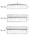
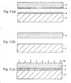
- Figs. 2 (a) to (c) and Figs. 3 (a) to (c) are cross-sectional views for schematically illustrating the method for producing this display device.
- a resin composition layer 4 is coated and formed by, for example, dropping a photocurable resin composition (hereinafter accordingly called “resin composition”, “resin” and the like) in a predetermined amount onto the surface of a display part 2 (step S1).
- a photocurable resin composition hereinafter accordingly called "resin composition”, “resin” and the like
- this resin composition layer 4 can also be formed by a printing method.
- a spacer for determining the distance between the display part 2 and a protective part 3 is not used.
- the distance between the display part 2 and the protective part 3 is determined by a positioning means (not shown).
- the present invention can also be applied in a case where a spacer can be used.
- a polarizing plate (not shown) is provided on the display part 2.
- a light-transmitting glass plate or a substrate formed from a polymer material (plastic) such as an acrylic resin (for example, PMMA: polymethyl methacrylate) may be suitably used as the protective part 3.
- Such a protective part 3 is lowered while being kept in a horizontal state.
- the protective part 3 is then fixed at a predetermined position by a not-shown positioning hoist mechanism.
- the resin composition 4 is placed and filled in a gap between the display part 2 and the protective part 3 (step S2).
- a resin composition which has, after curing, a transmittance of 90% or higher, a storage elastic modulus of 4.0 ⁇ 10 7 Pa or less at 25°C, and a curing shrinkage ratio of 5% or less is used as the photocurable resin composition.
- the viscosity of the photocurable resin composition is not especially limited. However, in light of the wet spreading speed and tendency not to run over (surface tension), the photocurable resin composition having preferably a viscosity of 1,000 mPa ⁇ s to 5,000 mPa ⁇ s, and more preferably 2,000 mPa ⁇ s to 3,000 mPa ⁇ s can be used.
- the photocurable resin composition may have a photoreactive acrylate material, such as polyurethane acrylate and isobornyl acrylate, and a photopolymerization initiator as main components, and may include another additive, such as a sensitizing agent, a plasticizer, transparent particles and the like within the scope of the object of the present invention.
- a photoreactive acrylate material such as polyurethane acrylate and isobornyl acrylate
- a photopolymerization initiator such as a photopolymerization initiator
- another additive such as a sensitizing agent, a plasticizer, transparent particles and the like within the scope of the object of the present invention.
- the photopolymerization initiator which includes 1-hydroxy-cyclohexyl-phenyl-ketone (sold under the name of "IRGACURE 184" manufactured by Ciba Specialty Chemicals Inc.) and the like may be preferably used.
- the protective part 3 may be provided with a UV-region cutting function in terms of protecting the display part 2 against UV rays.
- a photopolymerization initiator used in the present invention it is preferred to use a photopolymerization initiator that can cure the resin composition even in the visible light region (for example, sold under the name of "SPEEDCURE TPO" manufactured by Nihon Siber Hegner KK).
- the resin composition in the present invention is prepared so that the cured resin obtained by curing the resin composition with UV irradiation has a storage elastic modulus (25°C) of 4 ⁇ 10 7 Pa or less, and preferably of 1 ⁇ 10 3 to 1 ⁇ 10 5 Pa, a refractive index of preferably of 1.45 or more to 1.55 or less, and more preferably of 1.51 or more to 1.52 or less, and a transmittance of 90% or higher in the visible light region when the cured resin has 100 ⁇ m.
- a storage elastic modulus (25°C) of 4 ⁇ 10 7 Pa or less, and preferably of 1 ⁇ 10 3 to 1 ⁇ 10 5 Pa, a refractive index of preferably of 1.45 or more to 1.55 or less, and more preferably of 1.51 or more to 1.52 or less, and a transmittance of 90% or higher in the visible light region when the cured resin has 100 ⁇ m.
- the cured resin formed by curing such a curable resin composition may have a storage elastic modulus (25°C) that exceeds 4 ⁇ 10 7 Pa.
- a resin composition that forms such a cured resin is not included in the resin composition according to the present invention.
- This resin composition is prepared so as to have a curing shrinkage ratio of preferably 5.0% or less, more preferably 4.5% or less, especially preferably 4.0% or less, and still more preferably 0 to 2%. Consequently, the internal stress that builds up in the cured resin during curing of the resin composition can be reduced, and the distortion at the interface between the cured resin layer 4 and the display part 2 or the protective part 3 can be prevented.
- the amount of light scattered at the interface between the cured resin layer 4 and the display part 2 or the protective part 3 can be reduced. As a result, the luminance and the visibility of the display image can be improved.
- the magnitude of the internal stress that builds up in the cured resin during curing of this resin composition can be evaluated by dropping the resin composition onto a flat plate, curing the dropped resin composition, and measuring the average surface roughness of the resultant cured resin.
- the distortion generated at the interface between the display part or the protective part and the resin composition, when the resin composition is arranged between the display part and the protective part and the resin composition is cured can be ignored if, for example, a cured resin obtained by dropping 2 mg of the resin composition onto a glass plate or an acrylic plate and curing by UV irradiation to a 90% or higher cure ratio has an average surface roughness of 6.0 nm or less.
- this average surface roughness can be kept at 6.0 nm or less, preferably at 5.0 nm or less, and more preferably in the range of 1 to 3 nm.
- a glass plate the glass plate for sandwiching the liquid crystals of a liquid crystal cell or the glass plate used as a protective plate for the glass plate or the liquid crystal cell can be preferably used.
- an acrylic plate the acrylic plate used as the protective plate for a liquid crystal cell can be preferably used.
- These glass plates or acrylic plates usually have an average surface roughness of 1.0 nm or less.
- step S3 the presence of foreign substances or air bubbles mixed in the resin composition layer 4 which is filled between the display part 2 and the protective part 3 is checked.
- step S4 If, as the result of the check, it is confirmed that there is a defect, such as foreign substances or air bubbles being in the resin composition layer 4 between the display part 2 and the protective part 3 (step S4), the following repair operation is carried out.
- the display part 2 and the protective part 3 are separated by cutting the resin composition layer 4 using a wire 20 (step S5).
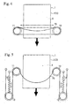
- Figs. 4 and 5 are explanatory diagrams showing examples of a method for cutting a resin composition layer according to the present invention.
- the wire 20 is passed over a pair of pulleys 10 and 11.
- the resin composition layer 4 between the display part 2 and the protective part 3 is pressed against the wire 20 while the wire 20 is slid in a left-right direction as shown in Fig. 4 , which is the width direction of the display part 2 and the protective part 3.
- the resin composition layer 4 is cut by moving a panel in a direction perpendicular to the wire 20, thereby separating the display part 2 and the protective part 3.
- the wire 20 is passed over a plurality of pulleys 10 to 13 which are arranged so as to constitute a pair of pulley blocks. Furthermore, tension springs 14 and 15, for absorbing slack in the wire 20 between the pulleys 10 and 11, are provided so as to link with each of the pulleys 12 and 13 which move as a pulley block.
- the resin composition layer 4 between the display part 2 and the protective part 3 is pressed against the wire 20.
- the resin composition layer 4 is cut by moving the panel 1 in a direction perpendicular to the wire 20, thereby separating the display part 2 and the protective part 3.
- the slack in the wire 20 between the pulleys 10 and 11 is absorbed by the elastic force of the tension springs 14 and 15, so that the wire 20 between the pulleys 10 and 11 is normally in a taut state.
- wire 20 used in the present invention it is preferred to use a metal wire made of carbon steel (for example, piano wire), or the like.
- the thickness of the wire 20 is not especially limited, as long as it is less than the thickness of the resin composition layer 4 between the display part 2 and the protective part 3. However, from the perspective of cutting performance, it is preferred to use a wire having a thickness of 50 ⁇ m to 100 ⁇ m.
- step S6 the resin composition remaining on the surfaces of the display part 2 and the protective part 3 is wiped away by a removing solution containing an organic solvent.
- Figs. 6 (a) and 6 (b) are explanatory diagrams schematically illustrating a method for wiping away a resin composition by an organic solvent.
- the organic solvent-containing removing solution as described below is coated by dropping or spraying, for example, onto the resin composition on the display part (for example, LCD cell) or protective part (for example, plastic plate or glass plate).
- the cured resin is wiped away using a wipe member formed of an elastomer or the like which is impregnated with the same solvent as the organic solvent of the removing solution that was coated on the cured resin.
- an organic solvent which is compatible when the resin composition and the organic solvent are mixed in a 1:1 volume ratio more specifically, an organic solvent having a small solubility parameter (SP value), can be suitably used.
- an organic solvent having the solubility parameter of less than 10 can be especially suitably used.
- the resin composition remaining on the surfaces of the display part 2 and the protective part 3 can be removed.
- organic solvents which do not cause damage, such as changes to the polarizing plate (formed of triacetyl cellulose) provided on the display part 2, for example.
- organic solvents which satisfy the above requirements, it is preferred to use limonene (C 6 H 10 , solubility parameter: 0.6), toluene (C 7 H 8 , solubility parameter: 8.8), or MEK (C 4 H 10 O, solubility parameter: 9.3).
- ethyl alcohol or isopropyl alcohol may be added to the removing solution of the present invention.
- limonene as the organic solvent.
- a substrate formed of a polymer material especially a PMMA substrate
- limonene as the organic solvent because the cured resin can be wiped away without causing changes to the substrate surface.
- the wiping properties and volatility can be improved by adding ethyl alcohol and/or isopropyl alcohol.
- the resin composition is wiped away by a wipe member formed of an elastomer or the like which is impregnated with the same organic solvent.
- step S7 the wiped surfaces of the display part 2 and the protective part 3 are examined by, for example, observation of changes in the appearance by a microscope. If there is no resin composition residue and no changes on the surface have occurred, the process returns to step S1, and the above-described steps are repeated from the start (step S8).
- step S8 if there is a resin composition residue remaining on the surfaces of the display part 2 and the protective part 3, or if surface changes have occurred, the produced display device is treated as a defective product, for example.
- step S4 if it is determined that foreign substances or air bubbles are not mixed in the resin composition layer 4 which is filled between the display part 2 and the protective part 3, the process proceeds to step S9.
- step S9 as shown in Fig. 3 (c) , for example, the resin composition is cured by irradiating UV rays via the protective part 3 on the resin composition layer 4.
- the irradiation direction of the UV rays is not especially limited. However, in order to achieve more uniform curing of the resin, it is preferable to irradiate UV rays in the direction perpendicular to the surface of the protective part 3 of the display part 2.
- UV rays may also be simultaneously directly irradiated from the external side face of the resin composition layer 4 between the display part 2 and the protective part 3, using an optical fiber or the like, for example.
- the display device was moved against the wire when cutting the resin composition layer.
- the wire may be moved against the display device.
- the display part and the protective part can also be separated by pulling them apart during the repair operation.
- the present invention is not limited to the above-described liquid crystal display device.
- the present invention may also be applied to various flat panel displays, such as an organic EL device.
- a resin composition was prepared by kneading in a kneader 70 parts by weight of an ester compound formed of a maleic anhydride adduct of a polyisoprene polymer and 2-hydroxyethyl methacrylate, 30 parts by weight of dicyclopentenyl oxyethyl methacrylate, 10 parts by weight of 2-hydroxybutyl methacrylate, 30 parts by weight of a hydrogenated terpene resin, 140 parts by weight of a butadiene polymer, 4 parts by weight of a photopolymerization initiator, and 0.5 parts by weight of a visible light region photopolymerization initiator.
- this resin composition was coated on a 100 ⁇ m-thick white glass plate to be used as a protective part or glass plate for an LCD cell to be used as a display part.
- limonene, toluene, or MEK was coated onto the resin composition as an organic solvent.
- the resin composition was then wiped away using a wipe member impregnated with the same solvent as the organic solvent coated on the resin composition.
- the resin composition could be wiped away when limonene was used as the organic solvent, a solvent residue was confirmed on the glass plate for an LCD cell. It was confirmed that this solvent residue was removed by ethanol without affecting the polarizing plate of the LCD cell.
- the above-described resin composition was dropped onto the above-described glass plate for a protective part for which the wiping step was finished.
- the plate was transported by a UV-conveyor into a UV-ray irradiation apparatus and then the resin was cured (thickness of the cured resin was 100 ⁇ m).
- the transmittance of this cured resin was measured using a UV-Visible Spectrophotometer (V-560, JASCO Corporation) and the measurement result was 90% or higher.
- the cured resin had a modulus of elasticity of 1 ⁇ 10 4 Pa and a curing shrinkage ratio of 1.8%. Consequently, the average surface roughness Ra was 2.7 nm, and the good results were obtained that there was hardly any distortion.
- a repair operation can be carried out easily and reliably without damage to the display part and the protective part. It is thus understood that a display device which is free from distortion can be obtained in a good yield.
Landscapes
- Physics & Mathematics (AREA)
- Nonlinear Science (AREA)
- Mathematical Physics (AREA)
- Chemical & Material Sciences (AREA)
- Crystallography & Structural Chemistry (AREA)
- General Physics & Mathematics (AREA)
- Optics & Photonics (AREA)
- Devices For Indicating Variable Information By Combining Individual Elements (AREA)
- Liquid Crystal (AREA)
- Electroluminescent Light Sources (AREA)
Abstract
Description
- The present invention generally relates to a display device, such as a liquid crystal display device (LCD), used in a cellular phone or the like, for example. In particular, the present invention relates to a technology for producing a display device provided with a transparent protective part on a display part.
- Conventionally, as this type of display device, a device like that shown in
Fig. 7 , for example, is known. As shown inFig. 7 , this liquidcrystal display device 101 is provided with a transparentprotective part 103 formed from, for example, glass or plastic, on a liquidcrystal display panel 102. In this case, to protect the surface of the liquidcrystal display panel 102 and a polarizing plate (not shown), agap 105 is formed between the liquidcrystal display panel 102 and theprotective part 103 by arranging aspacer 104 between the liquidcrystal display panel 102 and the protective part103. - However, the presence of the
gap 105 between the liquidcrystal display panel 102 and theprotective part 103 creates a decrease in contrast and luminance, which attributes to light scattering, and prevents production of a thinned panel. - In view of these problems, it has even been proposed to fill the gap between the liquid crystal display panel and the protective part with a resin (for example, see Patent Document 1).
- In cases where foreign substances or air bubbles are confirmed to have become mixed in the resin which is filled between such a display panel and a protective part, it is necessary to carry out a repair operation by peeling apart the display panel and the protective part.
- However, when peeling apart the display panel and the protective part, there is a risk of creating damage such as, resulting from scratching and cracking on the display panel and the protective part.
- Furthermore, it is quite difficult to completely remove a cured resin adhered to the display panel and the protective part with a solvent.
- In addition, though there are solvents which have high solubility against this kind of cured resin, such solvents have safety problems associated with them. Moreover, in order to completely remove this solvent itself, a separate washing step is required.
- Patent Document 1: Japanese Patent Application Laid-Open No.
2005-55641 - The present invention was made in consideration of such problems in the conventional art. Accordingly, it is an object of the present invention to provide a technology for producing a display device for which a repair operation can be carried out easily and reliably without damage to a display part and a protective part.
- In order to achieve the above object, the present invention is a method for producing a display device, the display device including a display part for displaying an image and a light-transmitting protective part provided on the display part, wherein a light-transmitting cured resin layer is arranged between the display part and the protective part. The method for producing a display device according to the present invention includes the steps of (A) a step of coating a resin composition, which is a raw material of the cured resin, on at least one of the display part or the protective part; (B) a step of closely adhering the display part and the protective part via the resin composition; and (C) a step of arranging the cured resin layer between the display part and the protective part by curing the resin composition by irradiating UV rays from external side of the protective part, wherein, if there is any defect in the display device after the step (B), the method further includes (b1) a step of separating the display part and the protective part; and (b2) a step of peeling and removing the resin composition adhered onto the separated display part and the separated protective part by a removing solution which contains an organic solvent.
- In the present invention, according to the above-described aspect of the invention, in the step (b1), the display part and the protective part are separated by coming into contact with a wire having a smaller diameter than a thickness of a resin composition layer from a side of the resin composition layer between the protective part and the display part; and moving the wire through the resin composition layer.
- In the present invention, according to the above-described aspect of the invention, the organic solvent is selected from a group of organic solvents which are compatible when the resin composition, before curing, and the organic solvent are mixed in a 1:1 volume ratio.
- In the present invention, according to the above-described aspect of the invention, the removing solution contains limonene or toluene as the organic solvent.
- In the present invention, according to the above-described aspect of the invention, the removing solution may also contain, in addition to limonene, ethyl alcohol or isopropyl alcohol as the organic solvent.
- In the present invention, the protective part is formed of a polymer material, and the removing solution contains limonene as the organic solvent. Even in this case, an advantageous effect can be obtained.
- In the present invention, according to the above-described aspect of the invention, there is an advantageous effect even when the display device can be a liquid crystal display device in which a polarizing plate is provided on a surface of the display part.
- In the present invention, after the display part and the protective part have been closely adhered with the resin composition layer interposed therebetween, if any defects are discovered before the curing of the resin, the display part and the protective part are separated. Furthermore, the resin composition adhered onto the separated display part and the separated protective part is peeled off and removed by a removing solution which contains an organic solvent. Consequently, according to the present invention, since a repair operation can be carried out before the curing of the resin, the display part and the protective part do not suffer from damage resulting from, for example, scratching and cracking.
- In the present invention, if the display part and the protective part are separated by coming into contact with a wire having a smaller diameter than the thickness of a resin composition layer, from a side face of the resin composition layer where the protective part and the display part are adhered, and moving the wire through the resin composition layer, a procedure for peeling off the display part and the protective part is not conducted during the repair operation. Thus, the display part and the protective part can be separated quickly without causing any damage to the display part and the protective part.
- In the present invention, by selecting an organic solvent which is compatible when the resin composition, before cutting, and the organic solvent are mixed in a 1:1 volume ratio as the organic solvent (for example, limonene or toluene), the resin composition adhered onto the separated display part and the separated protective part is dissolved, thereby carrying out the peeling smoothly and reliably.
- In the present invention, if a removing solvent containing ethyl alcohol or isopropyl alcohol can be used in addition to the organic solvent, such as limonene, the removing solution can improve the peeling properties of the resin composition. In addition, since the volatility of the removing solution increases, the removing solution can also improve operational efficiency.
- In the present invention, if step (b2) is carried out using limonene, and then the solvent residue is removed using ethyl alcohol or isopropyl alcohol, the repair operation can be carried out in a state where there is absolutely no residue on the display part and the protective part.
- According to the present invention, a repair operation can be carried out easily and quickly especially for a liquid crystal display device in which a polarizing plate is provided on the surface of a display part.
- Thus, according to the present invention, a technology can be provided for producing a display device for which a repair operation can be carried out easily and reliably without damage to a display part and a protective part.
-
-
Fig. 1 is a flow diagram illustrating an example of a method for producing a display device according to the present invention. -
Figs. 2 (a) to (c) are cross-sectional views schematically illustrating a method for producing a display device. -
Figs. 3 (a) to (c) are cross-sectional views schematically illustrating a method for producing a display device. -
Fig. 4 is an explanatory diagram illustrating an example of a method for cutting a resin composition layer according to the present invention. -
Fig. 5 is an explanatory diagram illustrating another example of a method for cutting a resin composition layer according to the present invention. -
Figs. 6 (a) and (b) are explanatory diagrams schematically illustrating a method wiping away a resin composition by an organic solvent. -
Fig. 7 is cross-sectional view illustrating a configuration of a conventional display device. - 2 ... Display part, 3... Protective part, 4... Resin composition layer
- Preferred embodiments of the present invention will now be described in more detail with reference to the drawings.
-
Fig. 1 is a flow diagram for illustrating an example of a method for producing a display device according to the present invention.Figs. 2 (a) to (c) andFigs. 3 (a) to (c) are cross-sectional views for schematically illustrating the method for producing this display device. - In the present embodiment, first, as shown in
Fig. 2 (a) , aresin composition layer 4 is coated and formed by, for example, dropping a photocurable resin composition (hereinafter accordingly called "resin composition", "resin" and the like) in a predetermined amount onto the surface of a display part 2 (step S1). - In the present invention, this
resin composition layer 4 can also be formed by a printing method. - In the present specification, a spacer for determining the distance between the
display part 2 and aprotective part 3 is not used. In the present specification, the distance between thedisplay part 2 and theprotective part 3 is determined by a positioning means (not shown). However, the present invention can also be applied in a case where a spacer can be used. - In the case of a liquid crystal display device, a polarizing plate (not shown) is provided on the
display part 2. In other embodiments, for example, a light-transmitting glass plate or a substrate formed from a polymer material (plastic) such as an acrylic resin (for example, PMMA: polymethyl methacrylate) may be suitably used as theprotective part 3. - Such a
protective part 3 is lowered while being kept in a horizontal state. Theprotective part 3 is then fixed at a predetermined position by a not-shown positioning hoist mechanism. As shown inFig. 2 (b) , theresin composition 4 is placed and filled in a gap between thedisplay part 2 and the protective part 3 (step S2). - In the present invention, a resin composition which has, after curing, a transmittance of 90% or higher, a storage elastic modulus of 4.0×10⁷ Pa or less at 25°C, and a curing shrinkage ratio of 5% or less is used as the photocurable resin composition.
- In the present invention, the viscosity of the photocurable resin composition is not especially limited. However, in light of the wet spreading speed and tendency not to run over (surface tension), the photocurable resin composition having preferably a viscosity of 1,000 mPa·s to 5,000 mPa·s, and more preferably 2,000 mPa·s to 3,000 mPa·s can be used.
- Specifically, for example, the photocurable resin composition may have a photoreactive acrylate material, such as polyurethane acrylate and isobornyl acrylate, and a photopolymerization initiator as main components, and may include another additive, such as a sensitizing agent, a plasticizer, transparent particles and the like within the scope of the object of the present invention.
- Here, the photopolymerization initiator which includes 1-hydroxy-cyclohexyl-phenyl-ketone (sold under the name of "IRGACURE 184" manufactured by Ciba Specialty Chemicals Inc.) and the like may be preferably used.
- The
protective part 3 may be provided with a UV-region cutting function in terms of protecting thedisplay part 2 against UV rays. In such a case, as the photopolymerization initiator used in the present invention, it is preferred to use a photopolymerization initiator that can cure the resin composition even in the visible light region (for example, sold under the name of "SPEEDCURE TPO" manufactured by Nihon Siber Hegner KK). - The resin composition in the present invention is prepared so that the cured resin obtained by curing the resin composition with UV irradiation has a storage elastic modulus (25°C) of 4×10⁷ Pa or less, and preferably of 1×10³ to 1×10⁵ Pa, a refractive index of preferably of 1.45 or more to 1.55 or less, and more preferably of 1.51 or more to 1.52 or less, and a transmittance of 90% or higher in the visible light region when the cured resin has 100 µm. Even when the main resin components constituting the resin composition are the same, if an additional resin component or monomer component combined to the main resin components is different, the cured resin formed by curing such a curable resin composition may have a storage elastic modulus (25°C) that exceeds 4×10⁷ Pa. However, a resin composition that forms such a cured resin is not included in the resin composition according to the present invention.
- This resin composition is prepared so as to have a curing shrinkage ratio of preferably 5.0% or less, more preferably 4.5% or less, especially preferably 4.0% or less, and still more preferably 0 to 2%. Consequently, the internal stress that builds up in the cured resin during curing of the resin composition can be reduced, and the distortion at the interface between the cured
resin layer 4 and thedisplay part 2 or theprotective part 3 can be prevented. - By arranging the resin composition between the
display part 2 and theprotective part 3 and then curing the resin composition, the amount of light scattered at the interface between the curedresin layer 4 and thedisplay part 2 or theprotective part 3 can be reduced. As a result, the luminance and the visibility of the display image can be improved. - The magnitude of the internal stress that builds up in the cured resin during curing of this resin composition can be evaluated by dropping the resin composition onto a flat plate, curing the dropped resin composition, and measuring the average surface roughness of the resultant cured resin. In practice, the distortion generated at the interface between the display part or the protective part and the resin composition, when the resin composition is arranged between the display part and the protective part and the resin composition is cured, can be ignored if, for example, a cured resin obtained by dropping 2 mg of the resin composition onto a glass plate or an acrylic plate and curing by UV irradiation to a 90% or higher cure ratio has an average surface roughness of 6.0 nm or less. However, according to the resin composition of the present invention, this average surface roughness can be kept at 6.0 nm or less, preferably at 5.0 nm or less, and more preferably in the range of 1 to 3 nm. With respect to a glass plate, the glass plate for sandwiching the liquid crystals of a liquid crystal cell or the glass plate used as a protective plate for the glass plate or the liquid crystal cell can be preferably used. Furthermore, with respect to an acrylic plate, the acrylic plate used as the protective plate for a liquid crystal cell can be preferably used. These glass plates or acrylic plates usually have an average surface roughness of 1.0 nm or less.
- After the above step S2, the presence of foreign substances or air bubbles mixed in the
resin composition layer 4 which is filled between thedisplay part 2 and theprotective part 3 is checked (step S3). - If, as the result of the check, it is confirmed that there is a defect, such as foreign substances or air bubbles being in the
resin composition layer 4 between thedisplay part 2 and the protective part 3 (step S4), the following repair operation is carried out. - In this case, in the present embodiment, as shown in
Figs. 2 (c) and3 (a) , thedisplay part 2 and theprotective part 3 are separated by cutting theresin composition layer 4 using a wire 20 (step S5). -
Figs. 4 and 5 are explanatory diagrams showing examples of a method for cutting a resin composition layer according to the present invention. - In the example shown in
Fig. 4 , thewire 20 is passed over a pair ofpulleys resin composition layer 4 between thedisplay part 2 and theprotective part 3 is pressed against thewire 20 while thewire 20 is slid in a left-right direction as shown inFig. 4 , which is the width direction of thedisplay part 2 and theprotective part 3. In this state, theresin composition layer 4 is cut by moving a panel in a direction perpendicular to thewire 20, thereby separating thedisplay part 2 and theprotective part 3. - On the other hand, in the example shown in
Fig. 5 , thewire 20 is passed over a plurality ofpulleys 10 to 13 which are arranged so as to constitute a pair of pulley blocks. Furthermore, tension springs 14 and 15, for absorbing slack in thewire 20 between thepulleys pulleys - In this example, the
resin composition layer 4 between thedisplay part 2 and theprotective part 3 is pressed against thewire 20. In this state, theresin composition layer 4 is cut by moving thepanel 1 in a direction perpendicular to thewire 20, thereby separating thedisplay part 2 and theprotective part 3. - In this case, the slack in the
wire 20 between thepulleys wire 20 between thepulleys - As the
wire 20 used in the present invention, it is preferred to use a metal wire made of carbon steel (for example, piano wire), or the like. - The thickness of the
wire 20 is not especially limited, as long as it is less than the thickness of theresin composition layer 4 between thedisplay part 2 and theprotective part 3. However, from the perspective of cutting performance, it is preferred to use a wire having a thickness of 50 µm to 100 µm. - After the
display part 2 and theprotective part 3 have thus been separated, the resin composition remaining on the surfaces of thedisplay part 2 and theprotective part 3 is wiped away by a removing solution containing an organic solvent (step S6). -
Figs. 6 (a) and 6 (b) are explanatory diagrams schematically illustrating a method for wiping away a resin composition by an organic solvent. - As shown in
Fig. 6 (a) , the organic solvent-containing removing solution as described below is coated by dropping or spraying, for example, onto the resin composition on the display part (for example, LCD cell) or protective part (for example, plastic plate or glass plate). - Furthermore, as shown in
Fig. 6 (b) , the cured resin is wiped away using a wipe member formed of an elastomer or the like which is impregnated with the same solvent as the organic solvent of the removing solution that was coated on the cured resin. - In the present invention, as the organic solvent contained in the removing solution, an organic solvent which is compatible when the resin composition and the organic solvent are mixed in a 1:1 volume ratio, more specifically, an organic solvent having a small solubility parameter (SP value), can be suitably used. In the present invention, an organic solvent having the solubility parameter of less than 10 can be especially suitably used.
- With a removing solution containing such an organic solvent, the resin composition remaining on the surfaces of the
display part 2 and theprotective part 3 can be removed. - Moreover, for a liquid crystal display device, it is preferred to use organic solvents, which do not cause damage, such as changes to the polarizing plate (formed of triacetyl cellulose) provided on the
display part 2, for example. - In the present invention, as organic solvents which satisfy the above requirements, it is preferred to use limonene (C6H10, solubility parameter: 0.6), toluene (C7H8, solubility parameter: 8.8), or MEK (C4H10O, solubility parameter: 9.3).
- In light of improvement of the wiping properties and volatility, ethyl alcohol or isopropyl alcohol may be added to the removing solution of the present invention.
- Among these, from the perspective of improving safety, it is preferred to use limonene as the organic solvent.
- When using, as the
protective part 2, a substrate formed of a polymer material (especially a PMMA substrate), it is preferred to use limonene as the organic solvent because the cured resin can be wiped away without causing changes to the substrate surface. - Further, if the organic solvent is limonene, the wiping properties and volatility can be improved by adding ethyl alcohol and/or isopropyl alcohol.
- Furthermore, after coating the removing solution on the resin composition, the resin composition is wiped away by a wipe member formed of an elastomer or the like which is impregnated with the same organic solvent.
- After the above wiping step, the wiped surfaces of the
display part 2 and theprotective part 3 are examined by, for example, observation of changes in the appearance by a microscope (step S7). If there is no resin composition residue and no changes on the surface have occurred, the process returns to step S1, and the above-described steps are repeated from the start (step S8). - On the other hand, in step S8, if there is a resin composition residue remaining on the surfaces of the
display part 2 and theprotective part 3, or if surface changes have occurred, the produced display device is treated as a defective product, for example. - Depending on the organic solvent contained in the removing solution, there may be a slight solvent residue. In such a case, it is preferred to carry out a post-washing with a solvent such as ethanol or the like , for example, which does not have an effect on the
display part 2 or theprotective part 3. - On the other hand, in the above-described step S4, if it is determined that foreign substances or air bubbles are not mixed in the
resin composition layer 4 which is filled between thedisplay part 2 and theprotective part 3, the process proceeds to step S9. In the step S9, as shown inFig. 3 (c) , for example, the resin composition is cured by irradiating UV rays via theprotective part 3 on theresin composition layer 4. - In the present invention, the irradiation direction of the UV rays is not especially limited. However, in order to achieve more uniform curing of the resin, it is preferable to irradiate UV rays in the direction perpendicular to the surface of the
protective part 3 of thedisplay part 2. - Furthermore, UV rays may also be simultaneously directly irradiated from the external side face of the
resin composition layer 4 between thedisplay part 2 and theprotective part 3, using an optical fiber or the like, for example. - The present invention is not limited to the above-described embodiment, and various modifications can be made thereto.
- For example, in the above-described embodiment, the display device was moved against the wire when cutting the resin composition layer. However, the present invention is not limited to this. The wire may be moved against the display device.
- In the present invention, since a repair operation is carried out before the resin is cured, the display part and the protective part can also be separated by pulling them apart during the repair operation.
- In addition, the present invention is not limited to the above-described liquid crystal display device. For example, the present invention may also be applied to various flat panel displays, such as an organic EL device.
- The present invention will now be described in more detail using the following embodiments and comparative examples. However, the present invention is not limited to the following.
- A resin composition was prepared by kneading in a kneader 70 parts by weight of an ester compound formed of a maleic anhydride adduct of a polyisoprene polymer and 2-hydroxyethyl methacrylate, 30 parts by weight of dicyclopentenyl oxyethyl methacrylate, 10 parts by weight of 2-hydroxybutyl methacrylate, 30 parts by weight of a hydrogenated terpene resin, 140 parts by weight of a butadiene polymer, 4 parts by weight of a photopolymerization initiator, and 0.5 parts by weight of a visible light region photopolymerization initiator.
- As shown in
Fig. 6 (a) , this resin composition was coated on a 100 µm-thick white glass plate to be used as a protective part or glass plate for an LCD cell to be used as a display part. - Then, as shown in
Fig. 6 (b) , limonene, toluene, or MEK was coated onto the resin composition as an organic solvent. - The resin composition was then wiped away using a wipe member impregnated with the same solvent as the organic solvent coated on the resin composition.
- Subsequently, the wiping properties of each sample were confirmed using a microscope based on observation of changes in the appearance. These results are shown in Table 1.
- In Table 1, samples which could be wiped without any problems in their appearance are marked with a "circle", while samples on which a slight amount of organic solvent was left are marked with a "triangle".
-

- It is clear from Table 1 that, for the glass plate serving as a protective part, when limonene, toluene, or MEK was used as the organic solvent, the wiping could be carried out without problems in appearance.
- However, for the glass plate for an LCD cell to be used as a display part, although the resin composition could be wiped away when limonene was used as the organic solvent, a solvent residue was confirmed on the glass plate for an LCD cell. It was confirmed that this solvent residue was removed by ethanol without affecting the polarizing plate of the LCD cell.
- The above-described resin composition was dropped onto the above-described glass plate for a protective part for which the wiping step was finished. The plate was transported by a UV-conveyor into a UV-ray irradiation apparatus and then the resin was cured (thickness of the cured resin was 100 µm).
- The transmittance of this cured resin was measured using a UV-Visible Spectrophotometer (V-560, JASCO Corporation) and the measurement result was 90% or higher.
- Next, using a viscoelastometer (DMS6100, Seiko Instruments Inc.), the modulus of elasticity (
measurement frequency 1 Hz, 25°C) of the cured resin was measured and the measurement result was 1.0×10⁴ Pa. - For the curing shrinkage ratio, specific gravities of the resin solution before curing and the cured solid product after curing was measured by an electronic densimeter (sold under the name of "SD-120L" manufactured by Mirage) and the curing shrinkage ratio was calculated by the following equation based on the difference of the specific gravities between the resin solution before curing and the cured solid product after curing. The curing shrinkage ratio was 1.8 %.

- 2 mg of the above resin composition was dropped onto the above-described glass plate for an LCD cell. The distortion (Ra: average surface roughness) in a given region (2.93 mm × 2.20 mm) of the glass plate surface due to the internal stress generated during the curing reaction by the UV irradiation was measured by a three-dimensional non-contact surface roughness meter (manufactured by Zygo K.K.) and the measurement result was 2.7 nm.
- Thus, in the present example, the cured resin had a modulus of elasticity of 1×10⁴ Pa and a curing shrinkage ratio of 1.8%. Consequently, the average surface roughness Ra was 2.7 nm, and the good results were obtained that there was hardly any distortion.
- Based on these results, according to the present invention, a repair operation can be carried out easily and reliably without damage to the display part and the protective part. It is thus understood that a display device which is free from distortion can be obtained in a good yield.
Claims (7)
- A method for producing a display device including a display part for displaying an image and a light-transmitting protective part provided on the display part, a light-transmitting cured resin layer being arranged between the display part and the protective part, the method comprising the steps of :(A) coating a resin composition, which is a raw material of the cured resin, on at least one of the display part or the protective part;(B) closely adhering the display part and the protective part via the resin composition; and(C) arranging the cured resin layer between the display part and the protective part by curing the resin composition by irradiating UV rays from an external side of the protective part,
wherein, if there is any defect in the display device after the step (B), the method further includes (b1) separating the display part and the protective part, and (b2) peeling and removing the resin composition adhered onto the separated display part and the separated protective part by a removing solution which contains an organic solvent. - The method for producing a display device according to claim 1, wherein, in the step (b1), the display part and the protective part are separated by coming into contact with a wire, the wire having smaller diameter than a thickness of a resin composition layer, from a side of the resin composition layer between the protective part and the display part, and moving the wire though the resin composition layer.
- The method for producing a display device according to claim 1, wherein the organic solvent is selected from among organic solvents which are compatible when the resin composition before curing and the organic solvent are mixed in a 1:1 volume ratio.
- The method for producing a display device according to claim 1, wherein the removing solution contains limonene or toluene as the organic solvent.
- The method for producing a display device according to claim 4, comprising, after carrying out the step (b2) using limonene, removing solvent residue using ethyl alcohol or isopropyl alcohol.
- The method for producing a display device according to claim 1, wherein the protective part is formed of a polymer material, and the removing solution contains limonene as the organic solvent.
- The method for producing a display device according to claim 1, wherein the display device is a liquid crystal display device in which a polarizing plate is provided on a surface of the display part.
Applications Claiming Priority (4)
| Application Number | Priority Date | Filing Date | Title |
|---|---|---|---|
| JP2007186360 | 2007-07-17 | ||
| JP2008005027 | 2008-01-11 | ||
| JP2008105108A JP5291973B2 (en) | 2007-07-17 | 2008-04-14 | Manufacturing method of display device |
| PCT/JP2008/062856 WO2009011370A1 (en) | 2007-07-17 | 2008-07-16 | Display manufacturing method |
Publications (3)
| Publication Number | Publication Date |
|---|---|
| EP2169457A1 true EP2169457A1 (en) | 2010-03-31 |
| EP2169457A4 EP2169457A4 (en) | 2010-08-04 |
| EP2169457B1 EP2169457B1 (en) | 2017-01-04 |
Family
ID=40259702
Family Applications (1)
| Application Number | Title | Priority Date | Filing Date |
|---|---|---|---|
| EP08778207.4A Active EP2169457B1 (en) | 2007-07-17 | 2008-07-16 | Display manufacturing method |
Country Status (7)
| Country | Link |
|---|---|
| US (1) | US8152945B2 (en) |
| EP (1) | EP2169457B1 (en) |
| JP (1) | JP5291973B2 (en) |
| KR (1) | KR101502642B1 (en) |
| CN (1) | CN101743506B (en) |
| TW (1) | TWI393941B (en) |
| WO (1) | WO2009011370A1 (en) |
Families Citing this family (19)
| Publication number | Priority date | Publication date | Assignee | Title |
|---|---|---|---|---|
| JPWO2010044291A1 (en) * | 2008-10-17 | 2012-03-15 | シャープ株式会社 | Display device and manufacturing method thereof |
| KR20160141876A (en) | 2009-10-16 | 2016-12-09 | 데쿠세리아루즈 가부시키가이샤 | Display device, process for manufacturing same, and transparent resin filler |
| JP5623754B2 (en) * | 2010-02-04 | 2014-11-12 | 株式会社ジャパンディスプレイ | Display device and manufacturing method thereof |
| KR101476063B1 (en) | 2010-06-21 | 2014-12-30 | 샤프 가부시키가이샤 | Display panel equipped with front plate, display device, and resin composition |
| KR101211371B1 (en) | 2010-09-16 | 2012-12-13 | 주식회사 토비스 | Method for manufacturing display panel with curved shape |
| JP5685149B2 (en) * | 2010-10-25 | 2015-03-18 | 富士フイルム株式会社 | Semi-cured product, cured product and production method thereof, optical component, cured resin composition |
| WO2012099171A1 (en) | 2011-01-18 | 2012-07-26 | シャープ株式会社 | Display panel with flat plate, method for manufacturing display panel with flat plate, and resin composition |
| JP2012172064A (en) | 2011-02-22 | 2012-09-10 | Nitto Denko Corp | Ultraviolet-curable optical resin adhesive composition |
| JP2013059711A (en) * | 2011-09-12 | 2013-04-04 | Japan Display East Inc | Cleaning method |
| MY170060A (en) | 2011-10-21 | 2019-07-02 | Nippon Kayaku Kk | Method for producing optical member and use of ultraviolet ray cured resin composition for same |
| JP5580806B2 (en) * | 2011-11-01 | 2014-08-27 | 東京エレクトロン株式会社 | Peeling apparatus, peeling system, peeling method, program, and computer storage medium |
| US10220537B2 (en) | 2012-10-17 | 2019-03-05 | Saxum, Llc | Method and apparatus for display screen shield replacement |
| JP6609093B2 (en) | 2013-05-13 | 2019-11-20 | 日東電工株式会社 | Hard coat film, polarizing plate and image display device |
| CN106463077B (en) * | 2014-07-01 | 2019-05-17 | 三菱化学株式会社 | Recycling method of optical member and reworkability evaluation method of optical laminate |
| JP6512682B2 (en) * | 2014-10-16 | 2019-05-15 | 藤森工業株式会社 | Peeling device and peeling method of bonded product |
| US9946104B2 (en) | 2015-12-28 | 2018-04-17 | Japan Display Inc. | Display device and method of manufacturing the same |
| JP6834609B2 (en) * | 2017-03-07 | 2021-02-24 | デクセリアルズ株式会社 | Manufacturing method of image display device |
| JP2019008156A (en) * | 2017-06-26 | 2019-01-17 | デクセリアルズ株式会社 | Method for reproducing transparent protective panel or image display member of image display device |
| JP6538252B1 (en) * | 2018-09-19 | 2019-07-03 | デクセリアルズ株式会社 | Method of manufacturing image display device |
Family Cites Families (17)
| Publication number | Priority date | Publication date | Assignee | Title |
|---|---|---|---|---|
| JP2812844B2 (en) * | 1992-11-30 | 1998-10-22 | シャープ株式会社 | Peeling device |
| JPH06345499A (en) * | 1993-06-08 | 1994-12-20 | Sekisui Chem Co Ltd | Method for recovering glass from laminated glass |
| JPH07114010A (en) * | 1993-10-14 | 1995-05-02 | Matsushita Electric Ind Co Ltd | Liquid crystal display |
| US5514294A (en) * | 1994-11-22 | 1996-05-07 | Alliedsignal Inc. | Limonene and tetrahydrofurfuryl alcohol cleaning agent |
| JPH10293314A (en) * | 1997-04-22 | 1998-11-04 | Toshiba Corp | Display device manufacturing method and manufacturing device |
| JPH1195210A (en) * | 1997-09-16 | 1999-04-09 | Optrex Corp | Method for peeling polarizing film and device therefor |
| JP2004184677A (en) * | 2002-12-03 | 2004-07-02 | Matsushita Electric Ind Co Ltd | Display panel separation method and display panel separation device |
| US7208206B2 (en) * | 2003-03-10 | 2007-04-24 | Nitto Denko Corporation | Glass crack prevention laminate and liquid crystal display device |
| JP2004325788A (en) * | 2003-04-24 | 2004-11-18 | Sony Corp | Optical inspection method and optical inspection device, and method for manufacturing liquid crystal display device |
| JP2005005029A (en) * | 2003-06-10 | 2005-01-06 | Matsushita Electric Ind Co Ltd | Separation method and separation apparatus for flat display device |
| JP2005055641A (en) | 2003-08-04 | 2005-03-03 | Yokogawa Electric Corp | Liquid crystal display |
| JP4370207B2 (en) | 2004-06-29 | 2009-11-25 | シャープ株式会社 | Liquid crystal display |
| JP2006184872A (en) * | 2004-12-03 | 2006-07-13 | Sony Corp | Liquid crystal display |
| JP2006169470A (en) * | 2004-12-20 | 2006-06-29 | Sanyo Chem Ind Ltd | Detergent used for electronics |
| JP4761293B2 (en) * | 2005-03-08 | 2011-08-31 | Jx日鉱日石エネルギー株式会社 | Cleaning composition and cleaning method |
| JP4431615B2 (en) * | 2005-07-11 | 2010-03-17 | 日立プラズマディスプレイ株式会社 | Flat panel display |
| JP4241697B2 (en) * | 2005-09-06 | 2009-03-18 | ユーテック株式会社 | Film peeling device |
-
2008
- 2008-04-14 JP JP2008105108A patent/JP5291973B2/en active Active
- 2008-07-16 KR KR1020107001010A patent/KR101502642B1/en active Active
- 2008-07-16 CN CN2008800247473A patent/CN101743506B/en active Active
- 2008-07-16 WO PCT/JP2008/062856 patent/WO2009011370A1/en not_active Ceased
- 2008-07-16 EP EP08778207.4A patent/EP2169457B1/en active Active
- 2008-07-17 TW TW097127142A patent/TWI393941B/en active
-
2010
- 2010-01-15 US US12/656,090 patent/US8152945B2/en active Active
Also Published As
| Publication number | Publication date |
|---|---|
| JP5291973B2 (en) | 2013-09-18 |
| WO2009011370A1 (en) | 2009-01-22 |
| TW200918999A (en) | 2009-05-01 |
| EP2169457B1 (en) | 2017-01-04 |
| TWI393941B (en) | 2013-04-21 |
| CN101743506A (en) | 2010-06-16 |
| KR101502642B1 (en) | 2015-03-13 |
| US20100210166A1 (en) | 2010-08-19 |
| CN101743506B (en) | 2011-09-14 |
| JP2009186961A (en) | 2009-08-20 |
| US8152945B2 (en) | 2012-04-10 |
| KR20100049030A (en) | 2010-05-11 |
| HK1141864A1 (en) | 2010-11-19 |
| EP2169457A4 (en) | 2010-08-04 |
Similar Documents
| Publication | Publication Date | Title |
|---|---|---|
| EP2169457B1 (en) | Display manufacturing method | |
| EP2169456B1 (en) | Display device manufacturing method | |
| KR101379126B1 (en) | Resin Compositions and Display Devices | |
| KR102023323B1 (en) | Display device, process for manufacturing same, and transparent resin filler | |
| EP2369570B1 (en) | Method for producing image display apparatus | |
| EP2133856A1 (en) | Method for manufacturing image display | |
| EP3594927B1 (en) | Method for manufacturing image display device | |
| JP5894557B2 (en) | Manufacturing method of display device | |
| HK1141865B (en) | Display device manufacturing method | |
| HK1141864B (en) | Display manufacturing method | |
| JP2014142648A (en) | Display device and manufacturing method of the same, and transparent resin filler |
Legal Events
| Date | Code | Title | Description |
|---|---|---|---|
| PUAI | Public reference made under article 153(3) epc to a published international application that has entered the european phase |
Free format text: ORIGINAL CODE: 0009012 |
|
| 17P | Request for examination filed |
Effective date: 20100115 |
|
| AK | Designated contracting states |
Kind code of ref document: A1 Designated state(s): AT BE BG CH CY CZ DE DK EE ES FI FR GB GR HR HU IE IS IT LI LT LU LV MC MT NL NO PL PT RO SE SI SK TR |
|
| AX | Request for extension of the european patent |
Extension state: AL BA MK RS |
|
| A4 | Supplementary search report drawn up and despatched |
Effective date: 20100705 |
|
| RIC1 | Information provided on ipc code assigned before grant |
Ipc: G02F 1/13 20060101ALI20100629BHEP Ipc: G02F 1/1333 20060101ALI20100629BHEP Ipc: G09F 9/00 20060101ALI20100629BHEP Ipc: G02F 1/1335 20060101AFI20090210BHEP |
|
| DAX | Request for extension of the european patent (deleted) | ||
| 17Q | First examination report despatched |
Effective date: 20120718 |
|
| RAP1 | Party data changed (applicant data changed or rights of an application transferred) |
Owner name: DEXERIALS CORPORATION |
|
| GRAP | Despatch of communication of intention to grant a patent |
Free format text: ORIGINAL CODE: EPIDOSNIGR1 |
|
| INTG | Intention to grant announced |
Effective date: 20160711 |
|
| GRAS | Grant fee paid |
Free format text: ORIGINAL CODE: EPIDOSNIGR3 |
|
| GRAA | (expected) grant |
Free format text: ORIGINAL CODE: 0009210 |
|
| AK | Designated contracting states |
Kind code of ref document: B1 Designated state(s): AT BE BG CH CY CZ DE DK EE ES FI FR GB GR HR HU IE IS IT LI LT LU LV MC MT NL NO PL PT RO SE SI SK TR |
|
| REG | Reference to a national code |
Ref country code: GB Ref legal event code: FG4D |
|
| REG | Reference to a national code |
Ref country code: CH Ref legal event code: EP |
|
| REG | Reference to a national code |
Ref country code: AT Ref legal event code: REF Ref document number: 859808 Country of ref document: AT Kind code of ref document: T Effective date: 20170115 |
|
| REG | Reference to a national code |
Ref country code: IE Ref legal event code: FG4D |
|
| REG | Reference to a national code |
Ref country code: DE Ref legal event code: R096 Ref document number: 602008048245 Country of ref document: DE |
|
| REG | Reference to a national code |
Ref country code: LT Ref legal event code: MG4D Ref country code: NL Ref legal event code: MP Effective date: 20170104 |
|
| REG | Reference to a national code |
Ref country code: AT Ref legal event code: MK05 Ref document number: 859808 Country of ref document: AT Kind code of ref document: T Effective date: 20170104 |
|
| PG25 | Lapsed in a contracting state [announced via postgrant information from national office to epo] |
Ref country code: NL Free format text: LAPSE BECAUSE OF FAILURE TO SUBMIT A TRANSLATION OF THE DESCRIPTION OR TO PAY THE FEE WITHIN THE PRESCRIBED TIME-LIMIT Effective date: 20170104 |
|
| PG25 | Lapsed in a contracting state [announced via postgrant information from national office to epo] |
Ref country code: LT Free format text: LAPSE BECAUSE OF FAILURE TO SUBMIT A TRANSLATION OF THE DESCRIPTION OR TO PAY THE FEE WITHIN THE PRESCRIBED TIME-LIMIT Effective date: 20170104 Ref country code: FI Free format text: LAPSE BECAUSE OF FAILURE TO SUBMIT A TRANSLATION OF THE DESCRIPTION OR TO PAY THE FEE WITHIN THE PRESCRIBED TIME-LIMIT Effective date: 20170104 Ref country code: GR Free format text: LAPSE BECAUSE OF FAILURE TO SUBMIT A TRANSLATION OF THE DESCRIPTION OR TO PAY THE FEE WITHIN THE PRESCRIBED TIME-LIMIT Effective date: 20170405 Ref country code: IS Free format text: LAPSE BECAUSE OF FAILURE TO SUBMIT A TRANSLATION OF THE DESCRIPTION OR TO PAY THE FEE WITHIN THE PRESCRIBED TIME-LIMIT Effective date: 20170504 Ref country code: NO Free format text: LAPSE BECAUSE OF FAILURE TO SUBMIT A TRANSLATION OF THE DESCRIPTION OR TO PAY THE FEE WITHIN THE PRESCRIBED TIME-LIMIT Effective date: 20170404 Ref country code: HR Free format text: LAPSE BECAUSE OF FAILURE TO SUBMIT A TRANSLATION OF THE DESCRIPTION OR TO PAY THE FEE WITHIN THE PRESCRIBED TIME-LIMIT Effective date: 20170104 |
|
| PG25 | Lapsed in a contracting state [announced via postgrant information from national office to epo] |
Ref country code: SE Free format text: LAPSE BECAUSE OF FAILURE TO SUBMIT A TRANSLATION OF THE DESCRIPTION OR TO PAY THE FEE WITHIN THE PRESCRIBED TIME-LIMIT Effective date: 20170104 Ref country code: ES Free format text: LAPSE BECAUSE OF FAILURE TO SUBMIT A TRANSLATION OF THE DESCRIPTION OR TO PAY THE FEE WITHIN THE PRESCRIBED TIME-LIMIT Effective date: 20170104 Ref country code: PT Free format text: LAPSE BECAUSE OF FAILURE TO SUBMIT A TRANSLATION OF THE DESCRIPTION OR TO PAY THE FEE WITHIN THE PRESCRIBED TIME-LIMIT Effective date: 20170504 Ref country code: BG Free format text: LAPSE BECAUSE OF FAILURE TO SUBMIT A TRANSLATION OF THE DESCRIPTION OR TO PAY THE FEE WITHIN THE PRESCRIBED TIME-LIMIT Effective date: 20170404 Ref country code: AT Free format text: LAPSE BECAUSE OF FAILURE TO SUBMIT A TRANSLATION OF THE DESCRIPTION OR TO PAY THE FEE WITHIN THE PRESCRIBED TIME-LIMIT Effective date: 20170104 Ref country code: PL Free format text: LAPSE BECAUSE OF FAILURE TO SUBMIT A TRANSLATION OF THE DESCRIPTION OR TO PAY THE FEE WITHIN THE PRESCRIBED TIME-LIMIT Effective date: 20170104 Ref country code: LV Free format text: LAPSE BECAUSE OF FAILURE TO SUBMIT A TRANSLATION OF THE DESCRIPTION OR TO PAY THE FEE WITHIN THE PRESCRIBED TIME-LIMIT Effective date: 20170104 |
|
| REG | Reference to a national code |
Ref country code: DE Ref legal event code: R097 Ref document number: 602008048245 Country of ref document: DE |
|
| PG25 | Lapsed in a contracting state [announced via postgrant information from national office to epo] |
Ref country code: SK Free format text: LAPSE BECAUSE OF FAILURE TO SUBMIT A TRANSLATION OF THE DESCRIPTION OR TO PAY THE FEE WITHIN THE PRESCRIBED TIME-LIMIT Effective date: 20170104 Ref country code: RO Free format text: LAPSE BECAUSE OF FAILURE TO SUBMIT A TRANSLATION OF THE DESCRIPTION OR TO PAY THE FEE WITHIN THE PRESCRIBED TIME-LIMIT Effective date: 20170104 Ref country code: CZ Free format text: LAPSE BECAUSE OF FAILURE TO SUBMIT A TRANSLATION OF THE DESCRIPTION OR TO PAY THE FEE WITHIN THE PRESCRIBED TIME-LIMIT Effective date: 20170104 Ref country code: EE Free format text: LAPSE BECAUSE OF FAILURE TO SUBMIT A TRANSLATION OF THE DESCRIPTION OR TO PAY THE FEE WITHIN THE PRESCRIBED TIME-LIMIT Effective date: 20170104 Ref country code: IT Free format text: LAPSE BECAUSE OF FAILURE TO SUBMIT A TRANSLATION OF THE DESCRIPTION OR TO PAY THE FEE WITHIN THE PRESCRIBED TIME-LIMIT Effective date: 20170104 |
|
| PLBE | No opposition filed within time limit |
Free format text: ORIGINAL CODE: 0009261 |
|
| STAA | Information on the status of an ep patent application or granted ep patent |
Free format text: STATUS: NO OPPOSITION FILED WITHIN TIME LIMIT |
|
| PG25 | Lapsed in a contracting state [announced via postgrant information from national office to epo] |
Ref country code: DK Free format text: LAPSE BECAUSE OF FAILURE TO SUBMIT A TRANSLATION OF THE DESCRIPTION OR TO PAY THE FEE WITHIN THE PRESCRIBED TIME-LIMIT Effective date: 20170104 |
|
| 26N | No opposition filed |
Effective date: 20171005 |
|
| PG25 | Lapsed in a contracting state [announced via postgrant information from national office to epo] |
Ref country code: SI Free format text: LAPSE BECAUSE OF FAILURE TO SUBMIT A TRANSLATION OF THE DESCRIPTION OR TO PAY THE FEE WITHIN THE PRESCRIBED TIME-LIMIT Effective date: 20170104 |
|
| REG | Reference to a national code |
Ref country code: CH Ref legal event code: PL |
|
| GBPC | Gb: european patent ceased through non-payment of renewal fee |
Effective date: 20170716 |
|
| REG | Reference to a national code |
Ref country code: IE Ref legal event code: MM4A |
|
| REG | Reference to a national code |
Ref country code: FR Ref legal event code: ST Effective date: 20180330 |
|
| PG25 | Lapsed in a contracting state [announced via postgrant information from national office to epo] |
Ref country code: CH Free format text: LAPSE BECAUSE OF NON-PAYMENT OF DUE FEES Effective date: 20170731 Ref country code: LI Free format text: LAPSE BECAUSE OF NON-PAYMENT OF DUE FEES Effective date: 20170731 Ref country code: IE Free format text: LAPSE BECAUSE OF NON-PAYMENT OF DUE FEES Effective date: 20170716 Ref country code: GB Free format text: LAPSE BECAUSE OF NON-PAYMENT OF DUE FEES Effective date: 20170716 |
|
| PG25 | Lapsed in a contracting state [announced via postgrant information from national office to epo] |
Ref country code: FR Free format text: LAPSE BECAUSE OF NON-PAYMENT OF DUE FEES Effective date: 20170731 |
|
| REG | Reference to a national code |
Ref country code: BE Ref legal event code: MM Effective date: 20170731 |
|
| PG25 | Lapsed in a contracting state [announced via postgrant information from national office to epo] |
Ref country code: LU Free format text: LAPSE BECAUSE OF NON-PAYMENT OF DUE FEES Effective date: 20170716 |
|
| PG25 | Lapsed in a contracting state [announced via postgrant information from national office to epo] |
Ref country code: BE Free format text: LAPSE BECAUSE OF NON-PAYMENT OF DUE FEES Effective date: 20170731 |
|
| PG25 | Lapsed in a contracting state [announced via postgrant information from national office to epo] |
Ref country code: MT Free format text: LAPSE BECAUSE OF NON-PAYMENT OF DUE FEES Effective date: 20170716 |
|
| PG25 | Lapsed in a contracting state [announced via postgrant information from national office to epo] |
Ref country code: MC Free format text: LAPSE BECAUSE OF FAILURE TO SUBMIT A TRANSLATION OF THE DESCRIPTION OR TO PAY THE FEE WITHIN THE PRESCRIBED TIME-LIMIT Effective date: 20170104 Ref country code: HU Free format text: LAPSE BECAUSE OF FAILURE TO SUBMIT A TRANSLATION OF THE DESCRIPTION OR TO PAY THE FEE WITHIN THE PRESCRIBED TIME-LIMIT; INVALID AB INITIO Effective date: 20080716 |
|
| PG25 | Lapsed in a contracting state [announced via postgrant information from national office to epo] |
Ref country code: CY Free format text: LAPSE BECAUSE OF NON-PAYMENT OF DUE FEES Effective date: 20170104 |
|
| PG25 | Lapsed in a contracting state [announced via postgrant information from national office to epo] |
Ref country code: TR Free format text: LAPSE BECAUSE OF FAILURE TO SUBMIT A TRANSLATION OF THE DESCRIPTION OR TO PAY THE FEE WITHIN THE PRESCRIBED TIME-LIMIT Effective date: 20170104 |
|
| PGFP | Annual fee paid to national office [announced via postgrant information from national office to epo] |
Ref country code: DE Payment date: 20250528 Year of fee payment: 18 |