EP2169430A1 - Power source device for detector, light or radiation detecting system having the device - Google Patents
Power source device for detector, light or radiation detecting system having the device Download PDFInfo
- Publication number
- EP2169430A1 EP2169430A1 EP07790837A EP07790837A EP2169430A1 EP 2169430 A1 EP2169430 A1 EP 2169430A1 EP 07790837 A EP07790837 A EP 07790837A EP 07790837 A EP07790837 A EP 07790837A EP 2169430 A1 EP2169430 A1 EP 2169430A1
- Authority
- EP
- European Patent Office
- Prior art keywords
- power supply
- power
- detector
- supply apparatus
- power supplies
- Prior art date
- Legal status (The legal status is an assumption and is not a legal conclusion. Google has not performed a legal analysis and makes no representation as to the accuracy of the status listed.)
- Ceased
Links
Images




Classifications
-
- A—HUMAN NECESSITIES
- A61—MEDICAL OR VETERINARY SCIENCE; HYGIENE
- A61B—DIAGNOSIS; SURGERY; IDENTIFICATION
- A61B6/00—Apparatus or devices for radiation diagnosis; Apparatus or devices for radiation diagnosis combined with radiation therapy equipment
- A61B6/02—Arrangements for diagnosis sequentially in different planes; Stereoscopic radiation diagnosis
- A61B6/03—Computed tomography [CT]
- A61B6/032—Transmission computed tomography [CT]
-
- A—HUMAN NECESSITIES
- A61—MEDICAL OR VETERINARY SCIENCE; HYGIENE
- A61B—DIAGNOSIS; SURGERY; IDENTIFICATION
- A61B6/00—Apparatus or devices for radiation diagnosis; Apparatus or devices for radiation diagnosis combined with radiation therapy equipment
- A61B6/56—Details of data transmission or power supply, e.g. use of slip rings
-
- A—HUMAN NECESSITIES
- A61—MEDICAL OR VETERINARY SCIENCE; HYGIENE
- A61B—DIAGNOSIS; SURGERY; IDENTIFICATION
- A61B6/00—Apparatus or devices for radiation diagnosis; Apparatus or devices for radiation diagnosis combined with radiation therapy equipment
- A61B6/58—Testing, adjusting or calibrating thereof
- A61B6/586—Detection of faults or malfunction of the device
-
- G—PHYSICS
- G01—MEASURING; TESTING
- G01T—MEASUREMENT OF NUCLEAR OR X-RADIATION
- G01T7/00—Details of radiation-measuring instruments
-
- H—ELECTRICITY
- H04—ELECTRIC COMMUNICATION TECHNIQUE
- H04N—PICTORIAL COMMUNICATION, e.g. TELEVISION
- H04N25/00—Circuitry of solid-state image sensors [SSIS]; Control thereof
- H04N25/30—Circuitry of solid-state image sensors [SSIS]; Control thereof for transforming X-rays into image signals
-
- A—HUMAN NECESSITIES
- A61—MEDICAL OR VETERINARY SCIENCE; HYGIENE
- A61B—DIAGNOSIS; SURGERY; IDENTIFICATION
- A61B2560/00—Constructional details of operational features of apparatus; Accessories for medical measuring apparatus
- A61B2560/02—Operational features
- A61B2560/0204—Operational features of power management
- A61B2560/0214—Operational features of power management of power generation or supply
Definitions
- This invention relates to a power supply apparatus for a detector for supplying power to a detector which detects light or radiation used in the medical field, and in industrial fields such as for nondestructive testing, RI (Radio isotope) inspection and optical inspection, and to a light or radiation detection system having the same.
- RI Radio isotope
- a flat panel detector (hereinafter simply called "FPD") is used as a detector for detecting light or radiation.
- the FPD includes a semiconductor layer, an application electrode, an active matrix substrate, a driver and a processor.
- the semiconductor layer converts light or radiation information into charge information.
- the application electrode is formed on a surface of the semiconductor layer to apply a high voltage power supply to the semiconductor layer.
- the active matrix substrate has a plurality of switching elements to read the charge information from the semiconductor layer.
- the driver drives this active matrix substrate for reading.
- the processor amplifies and digitizes the charge information read from the active matrix substrate.
- a power supply apparatus is connected to the FPD, and various power supplies are provided from the power supply apparatus.
- Fig. 5 is a view showing an outline construction of a power supply apparatus in a conventional example.
- the power supply apparatus 61 outputs two or more types of driving power supplies V1 provided for the driver, a plurality of processing power supplies V2 provided for the processor, and a high voltage power supply V3 provided for the application electrode.
- This power supply apparatus 61 includes a power output unit 63 formed of a plurality of output circuits 64 arranged on lines of the various power supplies V1, V2 and V3, respectively, to output the various power supplies V1, V2 and V3 individually.
- the power output unit 63 is controlled by a controller 65.
- An operating unit 71 is connected to the power supply apparatus 61.
- the operating unit 71 is formed of a computer having an input device such as a keyboard. When the user operates this operating unit 71, the operating unit 71 receives instructions to an FPD 75, and gives the received instructions to the controller 65.
- a utility power source 79 is connected to these power supply apparatus 61 and operating unit 71 through an uninterruptible power supply system (hereinafter simply called "UPS") 77.
- UPS uninterruptible power supply system
- the power supply apparatus 61 and operating unit 71 are operable with electric power supplied from the utility power source 79, and the UPS 77 accumulates electric power.
- the controller 65 outputs the various power supplies V1, V2 and V3 in a predetermined order. Consequently, the power supplies are successively provided for the driver and the like of the FPD 75.
- stop instructions are inputted to the operating unit 71, the controller 65 stops the output of the various power supplies in a predetermined order. Consequently, the power supplies for the driver and the like of the FPD 75 stop.
- the predetermined orders are decided for the purpose of protection of each circuit such as the driver of the FPD 75.
- the UPS 77 supplies electric power to the power supply apparatus 61 and operating unit 71. Consequently, the various power supplies are continuously provided for the FPD 75 from the power supply apparatus 61.
- the operating unit 71 also continues its operation to be able to receive instructions from the user. Therefore, when the user inputs stop instructions to the operating unit 71, the FPD 75 can be stopped normally.
- the power supplies are not stopped in an order other than the predetermined order, such as the output of the various power supplies to the FPD 75 stopping all at ounce. Therefore, the FPD 75 can be protected from damage, destruction or breakdown (see Patent Document 1. for example).
- the conventional example has an inconvenience that the UPS 77 is large-scaled which results in high cost. That is, it is desirable that the UPS 77 accumulates at least electric energy for operating the FPD 75 and operating unit 71 for several minutes. However, the UPS 77 having such an amount of accumulation of electricity becomes large-scaled, and it is difficult to secure its storage spice. Such large-capacity UPS 77 is expensive and is a cause of cost increase.
- This invention has been made having regard to the state of the art noted above, and its object is to provide a power supply apparatus for a detector, and a light or radiation detection system having the same, which can protect the detector even when a state of electric power supply from a utility power source becomes abnormal, without requiring a large-capacity uninterruptible power supply system.
- this invention provides the following construction.
- a power supply apparatus for a detector of this invention for providing a plurality of power supplies for a light or radiation detecting detector having a semiconductor layer for converting light or radiation information into charge information, an active matrix substrate having a plurality of switching elements for reading the charge information from the semiconductor layer, and a driving device for driving the active matrix substrate for reading, comprises a power output device capable of individually outputting the plurality of power supplies to be provided for the detector; a detection device for detecting a power supply state of a utility power source for operating the apparatus; a control device for carrying out an abnormal stopping process to stop the power supplies at the power output device in a predetermined order upon determination based on a result of detection by the detection device that an abnormality has occurred; and an electric storage device for supplying electric power to the control device, when the control device determines that an abnormality has occurred, to permit the control device to carry out the abnormal stopping process.
- the control device can directly monitor the power supply state of the utility power source. Since the electric storage device is provided for supplying electric power to the control device when the control device determines that an abnormality has occurred, the control device can appropriately carry out the abnormal stopping process for stopping the detector. This can prevent destruction, damage or breakdown of the detector. Since the electric storage device does not supply electric power to the entire power supply apparatus for a detector, the electric energy the electric storage device should accumulate is an extremely small amount. Therefore, a large-capacity uninterruptible power supply system is not required, whereby the power supply apparatus for a detector can be constructed at low cost. The control device automatically carries out the abnormal stopping process when the control device determines that an abnormality has occurred, and thus a manual operation is not required.
- the electric storage device is capable of continuing to supply electric power to the control device at least over a time required for the abnormal stopping process.
- the control device can carry out the abnormal stopping process reliably.
- the time required for the abnormal stopping process is at most one second. Since the abnormal stopping process is completed in a short time, the power supplies at the power output device can be stopped in a predetermined order.
- the electric storage device is capable of storing electric power to be consumed by the control device at least during the abnormal stopping process.
- the control device can carry out the abnormal stopping process conveniently.
- the electric storage device is an electric double layer capacitor.
- the electric storage device formed of an electric double layer capacitor can be charged and discharged quickly.
- the electric double layer capacitor can be charged and discharged only by time constant, and does not require a special circuit for charging and discharging unlike a battery. Since the electric double layer capacitor has a long life, it provides for excellent maintainability.
- the electric double layer capacitor has a capacitance of at least 1000 ⁇ F.
- the control device is fully permitted to carry out the abnormal stopping process, and the electric storage device can be made very compact.
- the detection device is arranged to detect a voltage of the utility power source.
- the power supply state of the utility power source can be detected properly.
- control device is arranged to determine that an abnormality has occurred, when the voltage detected by the detection device falls below a reference value.
- the control device can properly determine whether an abnormality has occurred.
- the power supplies the power output device is capable of individually outputting include a plurality of driving power supplies to be provided for the driving device; and in the abnormal stopping process, a driving power supply of highest voltage among the driving power supplies is stopped before the other driving power supplies. This can conveniently prevent destruction and damage of the driving device in time of the abnormal stopping process.
- the power supplies the power output device is capable of individually outputting include a plurality of driving power supplies to be provided for the driving device; the driving power supplies further include an ON-state voltage power supply for applying an ON-state voltage to set the switching elements to ON state; and in the abnormal stopping process, the ON-state voltage power supply is stopped before the other driving power supplies.
- the ON-state voltage of the ON-state voltage power supply is higher than voltages of the other driving power supplies.
- the driving device can be protected effectively.
- the driving device includes a drive circuit for switching provision and stopping of the ON-state voltage power supply for the switching elements, and a drive control circuit for controlling switching of the drive circuit; the ON-state voltage power supply is inputted to the drive circuit; and the other driving power supplies are inputted to one of the drive circuit and the drive control circuit.
- the drive circuit and drive control circuit can be protected effectively.
- the drive circuit comprises integrated circuits.
- the drive circuit can be formed conveniently.
- specifications of the integrated circuits provide that the other power supplies should be stopped after stopping the ON-state voltage power supply when stopping the plurality of power supplies to the integrated circuits. Where the integrated circuits with specifications defined in this way are used, the integrated circuits are effectively protected by carrying out the abnormal stopping process.
- the detector includes a processing device for processing the charge information read by the active matrix substrate; the power supplies the power output device is capable of individually outputting include a plurality of processing power supplies to be provided for the processing device; and in the abnormal stopping process, the ON-state voltage power supply is stopped before all the processing power supplies.
- the processing device includes at least amplifier circuits for amplifying the charge information, and an analog-to-digital converter circuit for digitizing output of the amplifier circuits; and the processing power supplies are inputted to the amplifier circuits and the analog-to-digital converter circuit, respectively.
- the amplifier circuits and the analog-to-digital converter circuit can be protected conveniently in time of the abnormal stopping process.
- the power supplies the power output device is capable of individually outputting include a high voltage power supply for applying a high voltage to the semiconductor layer; and in the abnormal stopping process, the high voltage power supply is stopped first among the power supplies the power output device is capable of individually outputting.
- the switching elements can be protected conveniently in time of the abnormal stopping process.
- a light or radiation detection system of this invention preferably, has a detector powered by the power supply apparatus for a detector for detecting light or radiation; wherein the detector comprises a semiconductor layer for converting light or radiation information into charge information; an active matrix substrate having a plurality of switching elements for reading the charge information from the semiconductor layer; and a driving device for driving the active matrix substrate for reading.
- the detector comprises a semiconductor layer for converting light or radiation information into charge information; an active matrix substrate having a plurality of switching elements for reading the charge information from the semiconductor layer; and a driving device for driving the active matrix substrate for reading.
- a light or radiation detection system of this invention preferably, has a detector powered by the power supply apparatus for a detector for detecting light or radiation; wherein the detector comprises a semiconductor layer for converting light or radiation information into charge information; an active matrix substrate having a plurality or switching elements for reading the charge information from the semiconductor layer; and a driving device for driving the active matrix substrate for reading; wherein the driving device includes a drive circuit for switching provision and stopping of the ON-state voltage power supply for the switching elements; and a drive control circuit for controlling switching of the drive circuit; and wherein the drive circuit comprises integrated circuits; and specifications of the integrated circuits provide that the other power supplies should be stopped after stopping the ON-state voltage power supply when stopping the plurality of power supplies to the integrated circuits.
- the drive circuit formed of the integrated circuits can be protected effectively in time of the abnormal stopping process.
- the light or radiation detection system of this invention is used exclusively for radiography.
- the light or radiation detection system is not continuously used such as in a surgical operation, insertion of a catheter or IVR.
- the control device when it determines that an abnormality has occurred, can automatically carry out the abnormal stopping process without causing any inconvenience.
- the control device can monitor the power supply state of the utility power source. Since the electric storage device is provided for supplying electric power to the control device when the control device determines that an abnormality has occurred, the control device can appropriately carry out the abnormal stopping process for stopping the detector. This can prevent destruction or breakdown of the detector. Since the electric storage device does not supply electric power to the entire power supply apparatus for a detector, the electric energy the electric storage device should secure can be greatly reduced. Therefore, a large-capacity uninterruptible power supply system is not required, whereby the power supply apparatus for a detector can be constructed at low cost. The abnormal stopping process is carried out automatically when the control device determines that an abnormality has occurred, and thus a manual operation is not required.
- the power supply apparatus for a detector for providing a plurality of power supplies for a light or radiation detecting detector having a semiconductor layer for converting light or radiation information into charge information, an active matrix substrate having a plurality of switching elements for reading the charge information from the semiconductor layer, and a driving device for driving the active matrix substrate for reading
- the power supply apparatus for a detector comprises a power output device capable of individually outputting the plurality of power supplies to be provided for the detector; a detection device for detecting a power supply state of a utility power source for operating the apparatus; a control device for carrying out an abnormal stopping process to stop the power supplies at the power output device in a predetermined order upon determination based on a result of detection by the detection device that an abnormality has occurred; and an electric storage device for supplying electric power to the control device, when the control device determines that an abnormality has occurred, to permit the control device to carry out the abnormal stopping process.
- Fig. 1 is a schematic outline view of an X-ray apparatus according to the embodiment.
- the X-ray apparatus in the embodiment has, applied thereto, a power supply apparatus for a detector, and a light or radiation detection system having the same, according to this invention.
- This apparatus is an apparatus for X-raying a patient M in the medical field.
- This apparatus includes a top board 1, an X-ray tube 3 and a flat panel X-ray detector (hereinafter simply called "FPD") 5.
- the patient M is placed on the top board 1.
- the top board 1 is formed of an X-ray transmissive material, for example.
- the X-ray tube 3 and FPD 5 are opposed to each other across the top board 1.
- the X-ray tube 3 emits X-rays to the patient M.
- the FPD 5 detects X-rays transmitted through the patient M.
- the FPD 5 corresponds to the detector in this invention.
- a power supply apparatus 7 is connected to the FPD 5.
- the power supply apparatus 7 is constructed capable of outputting a plurality of power supplies (described hereinafter) individually to the FPD 5.
- An operating unit 9 is connected to the power supply apparatus 7.
- the operating unit 9 is formed of a computer having an input device such as a keyboard. When the user operates this operating unit 9, the operating unit 9 receives instructions for starting and stopping the FPD 5, for example. The instructions received are outputted to the power supply apparatus 7.
- a utility power source 10 is connected to these power supply apparatus 7 and operating unit 9.
- the utility power source 10 is a commercial power source (AC100V), for example.
- the utility power source 10 supplies electric power to the power supply apparatus 7 and operating unit 9 for operation.
- the power supply apparatus 7 corresponds to the power source for a detector in this invention.
- the power supply apparatus 7 and FPD 5 correspond to the light or radiation detection system in this invention.
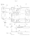
- Fig. 2 is a plan view showing a principal portion of the FPD.
- Fig. 3 is a view schematically showing an equivalent circuit of the principal portion of the FPD.
- Fig. 4 is a schematic view showing an equivalent circuit of an active matrix substrate as corresponding to its section.
- the FPD 5 is the direct conversion type and includes a semiconductor layer 11 for directly converting X-ray information into charge information.
- the semiconductor layer 11 is formed of amorphous selenium (a-Se), for example.
- An application electrode 13 for applying a high voltage to the semiconductor layer 11 is laminated on an X-ray incident surface of the semiconductor layer 11.
- An active matrix substrate 15 is formed on the back surface of the semiconductor layer 11.
- the active matrix substrate 15 has a plurality of switching elements s as described hereinafter, to read the charge information converted by the semiconductor layer 11.
- Driving flexible substrates 17 are connected to one side of the active matrix substrate 15. Processing flexible substrates 19 are connected to another side.
- Integrated circuits (ICs) 21 are mounted on the driving flexible substrates 17. These integrated circuits 21 constitute a drive circuit 21c for switching provision and stopping of ON-state voltage power supply Vdd which sets the switching elements s to ON state. More particularly, ON-state voltage power supply Vdd and OFF-state voltage power supply Vee are inputted to the drive circuit, and the drive circuit 21c is constructed capable of selectively outputting these ON-state voltage power supply Vdd and OFF-state voltage power supply Vee. Here, the OFF-state voltage power supply Vee sets the switching elements s to OFF state.
- the other ends of the driving flexible substrates 17 are connected to a driving printed circuit board 23.
- a drive control circuit 23c is formed on the driving printed circuit board 23 for controlling switching of the drive circuit 21c.
- a controlling power supply Vc is inputted to this drive control circuit 23c.
- the drive control circuit 23c outputs to the drive circuit 21c a signal for controlling switching of the drive circuit 21c.
- the driving flexible substrates 17, integrated circuits 21 (drive circuit 21c) and driving printed circuit board 23 (drive control circuit 23c) correspond to the driving device in this invention.
- Integrated circuits (ICs) 25 are mounted also on the processing flexible substrates 19. Each integrated circuit 25 acts as an amplifier circuit 25c for amplifying the charge information read from the active matrix substrate 15. An amplification power supply Vam is inputted to this amplifier circuit 25c. The other ends of the processing flexible substrates 19 are connected to a processing printed circuit board 27. An analog-to-digital converter 27c is formed on the processing printed circuit board 27 for digitizing output (analog) of the amplifier circuits 25c. An A/D conversion power supply Vad is inputted to the analog-to-digital converter 27c.
- the processing flexible substrates 19, integrated circuits 25 (amplifier circuits 25c) and processing printed circuit board 27 (analog-to-digital converter 27c) correspond to the processing device in this invention. The analog-to-digital converter 27c corresponds to the analog-to-digital conversion circuit in this invention.
- the active matrix substrate 15 is a transparent glass substrate having electrical insulation property.
- the active matrix substrate 15 has, formed thereon, a plurality of split electrodes 31 for collecting the charge information converted by the semiconductor layer 11.
- the split electrodes 31 are separated and arranged along rows and columns which are the two crossing axial directions.
- a capacitor Ca is connected to each split electrode 31 for stoping the charge information.
- the switching elements s are connected to respective pairs of split electrode 31 and capacitor Ca.
- the switching elements s are formed of thin film transistors, for example.
- the active matrix substrate 15 has a gate line 33 laid for each row of detecting elements d, and a data line 35 laid for each column of switching elements s.
- Each gate line 33 is connected commonly to the gates of the switching element s in each row.
- the other ends of the gate lines 33 are electrically connected to the driving flexible substrates 17, and are drawn out of the active matrix substrate 15.
- Each data line 35 is connected commonly to the drains of the switching elements s in each column.
- the other ends of the data lines 35 are electrically connected to the processing flexible substrates 19, and are drawn out of the active matrix substrate 15.
- the FPD 5 constructed in this way operates as follows.
- the semiconductor layer 11 converts the emitted X-rays (X-ray information) to the charge information.
- the drive circuit 21c provides OFF-state voltage power supply Vee for the switching elements s under control of the drive control circuit 23c, the switching elements s remain in OFF state. Therefore, the charge information converted by the semiconductor layer 11 is stored in the capacitors Ca.
- ON-state voltage power supply Vdd is outputted to one gate line 33 from the drive circuit 21c under control of the drive control circuit 23c, the switching elements s connected to the gate line 33 will be turned on en bloc.
- each capacitor Ca is read to the data lines 35 via each switching element s.
- the read charge information is amplified by each amplifier circuit 25c.
- the analog information amplified by each amplifier circuit 25c is digitized by the analog-to-digital converter 27c.
- the digitized information is further subjected to various processes to become X-ray images.
- the power supply apparatus 7 includes a detection unit 41, a power conversion unit 43, a power output unit 45, a controller 49 and an electric storage unit 51.
- the detection unit 41 detects voltage of the electric power supplied from the utility power source 10, and outputs a detection result to the controller 49.
- the power conversion unit 43 converts the electric power supplied from the utility power source 10 to direct current and to a predetermined voltage. And it outputs ON-state voltage power supply Vdd, OFF-state voltage power supply Vee, controlling power supply Vc, amplification power supply Vam and A/D conversion power supply Vad noted hereinbefore.
- This power conversion unit 43 is realized, as appropriate, by an AC-DC conversion circuit or DC-DC conversion circuit, a filter, a feedback circuit or the like.
- ON-state voltage power supply Vdd, OFF-state voltage power supply Vee and controlling power supply Vc are all for driving the active matrix substrate 15 and reading the charge information, and will be called “driving power supplies” as appropriate.
- Amplification power supply Vam and A/D conversion power supply Vad are for processing the charge information read from the active matrix substrate 15, and will be called “processing power supplies” as appropriate.
- each driving power supply and each processing power supply are direct-current power supplies of low voltage (several tens of volts or less), which will be called collectively “low voltage power supplies”. Among the low voltage power supplies, the voltage of ON-state voltage power supply Vdd is the highest.
- the power output unit 45 has driving output circuits 46a, 46b and 46c for switching output and stopping of the driving power supplies (Vdd, Vee, Vc) obtained from the power conversion unit 43. It has also processing output circuits 47a and 47b for switching output and stopping of the processing power supplies (Vam, Vad) obtained from the power conversion unit 43.
- the driving output circuits 46a, 46b ..., whin not distinguished, will be referred to hereinafter as driving output circuits 46.
- the processing output circuits 47a and 47b when not distinguished, will be referred to hereinafter as processing output circuits 47.
- Each driving output circuit 46 and each processing output circuit 47 are formed of relays arranged on lines of low voltage power supplies for opening and closing the lines.
- the power output unit 45 has a high voltage output circuit 48.
- the high voltage output circuit 48 is formed of a booster circuit (not shown) for converting the electric power supplied from the utility power source 10 to direct-current high voltage, and a voltage varying part (not shown) for varying the voltage boosted by this booster circuit.
- the high voltage output circuit 48 outputs high voltage power supply Vh.
- the voltage of high voltage power supply Vh is about several 100V to several 10kV. High voltage powder supply Vh outputted is provided for the application electrode 13 noted hereinbefore.
- the controller 49 controls the power output unit 45. Specifically, it controls each of the driving and processing output circuits 46 and 47 and the high voltage output circuit 48. Thus, the controller 49 causes the various power supplies to be outputted in a predetermined order to start the FPD 5 (starting process). The FPD 5 is stopped by stopping output of the various power supplies in a predetermined order (stopping process). Further, a comparison is made between a result of detection by the detection unit 41 and a reference value set beforehand, to determine whether or not the power supply state of the utility power source 10 is abnormal. When the controller 49 determines that it is abnormal, the FPD 5 is stopped by stopping output of the various power supplies in a predetermined order (abnormal stopping process). Each predetermined order noted above is set beforehand according to the starting, stopping or abnormal stopping.
- Such controller 49 is realized by a storage medium such as a fixed disk which stores a program specifying the predetermined orders according to starting, stopping and abnormal stopping and a variety of information such as the reference value for comparison with detection results, a central processing unit (CPU) which performs various processes based on this program, and a RAM (Random-Access Memory) used as workspace for arithmetic processes and the like.
- a storage medium such as a fixed disk which stores a program specifying the predetermined orders according to starting, stopping and abnormal stopping and a variety of information such as the reference value for comparison with detection results
- CPU central processing unit
- RAM Random-Access Memory
- the electric storage unit 51 accumulates the electric power supplied from the utility power source 10 at normal times when the power is supplied at a predetermined voltage from the utility power source 10. When the controller 49 determines that an abnormality has occurred, the electric storage unit 51 supplies power to the controller 49.
- This electric storage unit 51 preferably, is an electric double layer capacitor.
- the electric double layer capacitor is also called a super capacitor.
- the capacitance of the electric double layer capacitor is designed or selected to be capable of continuing to supply power to the controller 49 over a time required for the abnormal stopping process. Specifically, at least 1000 ⁇ F is preferred.
- the power supply apparatus 7 and operating unit 9 are in operation with electric power supplied from the utility power source 10 to the power supply apparatus 7 and operating unit 9.
- the user inputs startup instructions to the operating unit 9.
- the operating unit 9 receives the startup instructions and gives the received startup instructions to the controller 49.
- the power conversion unit 43 converts the electric power supplied from the utility power source 10, and outputs each low voltage power supply.
- the controller 49 controls the power output unit 45 to first output OFF-state voltage power supply Vee, controlling power supply Vc and processing power supplies (Vam, Vad).
- OFF-state voltage power supply Vee is provided for the drive circuit 21c
- controlling power supply Vc is provided for the drive control circuit 23c.
- a signal for controlling switching of the drive circuit 21c is inputted from the drive control circuit 23c to the drive circuit 21c.
- Amplification power supply Vam is provided for the amplifier circuits 25c, and A/D conversion power supply Vad is provided for the analog-to-digital converter 27c.
- the controller 49 controls the power output unit 45 to output ON-state voltage power supply Vdd.
- ON-state voltage power supply Vdd is provided for the drive circuit 21c.
- the controller 49 controls the power output unit 45 to output high voltage power supply Vh.
- high voltage power supply Vh is provided for the application electrode 13. This completes starting of the FPD 5.
- Alter the FPD 5 is started, an operation by the user causes the X-ray tube 3 to emit X-rays to the patient M, and causes the FPD 5 to detect X-rays transmitted through the patient M. X-ray images of the patient M are created based on detection results of the FPD 5. In this way, X radiography of the patient M is carried out as appropriate.
- the user inputs stop instructions to the operating unit 9.
- the operating unit 9 receives the stop instructions, and gives them to the controller 49.
- the controller 49 controls the power output unit 45 to stop the output of high voltage power supply Vh first. This results in a state where high voltage power supply Vh is not applied to the application electrode 13.
- the controller 49 controls the power output unit 45 to stop the output of ON-state voltage power supply Vdd. As a result, the provision of ON-state voltage power supply Vdd for the drive circuit 21c is stopped.
- the controller 49 controls the power output unit 45 to stop the output of each of OFF-state voltage power supply Vee, controlling power supply Vc and processing power supplies (Vam, Vad).
- the detection unit 41 detects the supply voltage of the utility power source 10, and outputs it to the controller 49.
- the controller 49 determines whether an abnormality has occurred, from the result of a comparison of the detection result with the reference value. When a power failure or instantaneous interruption occurs to lower the supply voltage of the utility power source 10 below the reference value, the controller 49 determines that an abnormality has occurred. In this case, in place of the utility power source 10, the electric storage unit 51 begins to supply power to the controller 49.
- the controller 49 controls the power output unit 45 to stop the output of high voltage power supply Vh first. When the output of high voltage power supply Vh has been stopped, the output of ON-state voltage power supply Vdd is stopped next.
- the time from when the controller 49 determines that an abnormality has occurred until the abnormal stopping process is completed is relatively short. Since the power conversion unit 43 has an AC-DC conversion circuit or DC-DC conversion circuit, the voltage of the various low voltage power supplies outputted from the power conversion unit 43 is maintained for a relatively short period even when the supply voltage of the utility power source 10 falls. Therefore, even when the supply voltage of the utility power source 10 falls, the various power supplies successively stop in the predetermined order according to the abnormal stopping process.
- the X-ray apparatus with the power supply apparatus 7 having the detection unit 41, can conveniently detect the power supply state of the utility power source 10. Since the detection result of the detection unit 41 is directly inputted to the controller 49, the controller 49 can conveniently determine whether the power supply state is abnormal or not. When an abnormality is found, the electric storage unit 51 supplies power to the controller 49 whereby the controller 49 can carry out the abnormal stopping process reliably. That is, the various power supplies provided for the FPD 5 can be stopped successively in the predetermined order. Consequently, damage or breaking of each circuit of the FPD 5 can be prevented conveniently.
- the drive circuit 21c and drive control circuit 23c can be protected conveniently by stopping the provision of ON-state voltage power supply Vdd having the highest voltage among the driving power supplies (Vdd, Vee, Vc), before the other driving power supplies (Vee, Vc).
- Vdd ON-state voltage power supply
- the integrated circuits (ICs) 21 forming the drive circuit 21c provide that the other power supplies should be stopped after stopping ON-state voltage power supply Vdd when stopping the plurality of power supplies to these integrated circuits (ICs) 21, the integrated circuits (ICs) 21 can be protected effectively.
- Each circuit of the FPD 5 can be enhanced more reliably by stopping the provision of ON-state voltage power supply Vdd before the processing power supplies (Vam, Vad) in the abnormal stopping process.
- the switching elements s can be protected conveniently by stopping the provision of high voltage power supply Vh before the low voltage power supplies (Vdd, Vee, Vc, Vam, Vad) in the abnormal stopping process.
- high voltage power supply Vh is provided even after the provision of the low voltage power supplies is stopped, there occurs a possibility that the potential of the switching elements s increases to destroy the switching elements s.
- the abnormal stopping process in this embodiment can officially prevent such destruction of the switching elements s.
- the electric storage unit 51 in this embodiment may accumulate only the power consumed by the controller 49 in carrying out the abnormal stopping process, the capacity of the electric storage unit 51 can be made very small. Thus, it is unnecessary to provide a largo-capacity uninterruptible power supply system as in the conventional example. Therefore, the power supply apparatus 7 can be made compact, and the manufacturing cost of the power supply apparatus 7 can be reduced.
- the electric storage unit 51 in this embodiment which is formed of an electric double layer capacitor, can be charged and discharged quickly.
- the electric double layer capacitor can be charged and discharged only by time constant, and does not require a special circuit for charging and discharging unlike a battery.
- the circuit of the electric storage unit 51 can be constructed simply and easily. Since the electric double layer capacitor has a long life, it can improve maintainability of the power supply apparatus 7.
- the detention unit 41 in this embodiment detects the voltage of the utility power source 10, it can conveniently detect abnormalities such as a power failure and instantaneous interruption that lower the voltage of the utility power source 10.
- the controller 49 can appropriately determine whether or not the power supply state of the utility power source 10 is abnormal by comparing the predetermined reference value and detection results of the detection unit 41.
- the controller 49 automatically carries out the abnormal stopping process when it determines that an abnormality has occurred, a manual operation such as the user operating the operating unit 9 is not required.
- the X-ray apparatus in this embodiment preferably, is a special-purpose machine for radiography. Since the X-ray apparatus is not continuously used such as in a surgical operation, insertion of a catheter or IVR if it is a special-purpose machine for radiography, the controller 49 can automatically carry out the abnormal stopping process without causing any inconvenience.
- the X-tray apparatus is not limited to use as a special-purpose machine for radiography, but may have various uses.
Landscapes
- Health & Medical Sciences (AREA)
- Life Sciences & Earth Sciences (AREA)
- Engineering & Computer Science (AREA)
- Medical Informatics (AREA)
- High Energy & Nuclear Physics (AREA)
- Physics & Mathematics (AREA)
- Molecular Biology (AREA)
- Pathology (AREA)
- Surgery (AREA)
- Veterinary Medicine (AREA)
- Biophysics (AREA)
- Public Health (AREA)
- Nuclear Medicine, Radiotherapy & Molecular Imaging (AREA)
- Optics & Photonics (AREA)
- General Health & Medical Sciences (AREA)
- Radiology & Medical Imaging (AREA)
- Biomedical Technology (AREA)
- Heart & Thoracic Surgery (AREA)
- Animal Behavior & Ethology (AREA)
- General Physics & Mathematics (AREA)
- Multimedia (AREA)
- Signal Processing (AREA)
- Spectroscopy & Molecular Physics (AREA)
- Computer Networks & Wireless Communication (AREA)
- Pulmonology (AREA)
- Theoretical Computer Science (AREA)
- Measurement Of Radiation (AREA)
- Protection Of Static Devices (AREA)
Abstract
Description
- This invention relates to a power supply apparatus for a detector for supplying power to a detector which detects light or radiation used in the medical field, and in industrial fields such as for nondestructive testing, RI (Radio isotope) inspection and optical inspection, and to a light or radiation detection system having the same.
- Conventionally, a flat panel detector (hereinafter simply called "FPD") is used as a detector for detecting light or radiation. The FPD includes a semiconductor layer, an application electrode, an active matrix substrate, a driver and a processor. The semiconductor layer converts light or radiation information into charge information. The application electrode is formed on a surface of the semiconductor layer to apply a high voltage power supply to the semiconductor layer. The active matrix substrate has a plurality of switching elements to read the charge information from the semiconductor layer. The driver drives this active matrix substrate for reading. The processor amplifies and digitizes the charge information read from the active matrix substrate. A power supply apparatus is connected to the FPD, and various power supplies are provided from the power supply apparatus.
- Reference is made to
Fig. 5. Fig. 5 is a view showing an outline construction of a power supply apparatus in a conventional example. Thepower supply apparatus 61 outputs two or more types of driving power supplies V1 provided for the driver, a plurality of processing power supplies V2 provided for the processor, and a high voltage power supply V3 provided for the application electrode. Thispower supply apparatus 61 includes apower output unit 63 formed of a plurality ofoutput circuits 64 arranged on lines of the various power supplies V1, V2 and V3, respectively, to output the various power supplies V1, V2 and V3 individually. Thepower output unit 63 is controlled by acontroller 65. - An
operating unit 71 is connected to thepower supply apparatus 61. Theoperating unit 71 is formed of a computer having an input device such as a keyboard. When the user operates thisoperating unit 71, theoperating unit 71 receives instructions to an FPD 75, and gives the received instructions to thecontroller 65. Autility power source 79 is connected to thesepower supply apparatus 61 andoperating unit 71 through an uninterruptible power supply system (hereinafter simply called "UPS") 77. - In the conventional example constructed in this way, the
power supply apparatus 61 andoperating unit 71 are operable with electric power supplied from theutility power source 79, and the UPS 77 accumulates electric power. When the user inputs startup instructions to theoperating unit 71, thecontroller 65 outputs the various power supplies V1, V2 and V3 in a predetermined order. Consequently, the power supplies are successively provided for the driver and the like of the FPD 75. When stop instructions are inputted to theoperating unit 71, thecontroller 65 stops the output of the various power supplies in a predetermined order. Consequently, the power supplies for the driver and the like of the FPD 75 stop. The predetermined orders are decided for the purpose of protection of each circuit such as the driver of the FPD 75. - When an instantaneous interruption or power failure occurs and the voltage of the
utility power source 79 falls, the UPS 77 supplies electric power to thepower supply apparatus 61 andoperating unit 71. Consequently, the various power supplies are continuously provided for the FPD 75 from thepower supply apparatus 61. Theoperating unit 71 also continues its operation to be able to receive instructions from the user. Therefore, when the user inputs stop instructions to theoperating unit 71, the FPD 75 can be stopped normally. Thus, even when theutility power source 79 undergoes a voltage drop, the power supplies are not stopped in an order other than the predetermined order, such as the output of the various power supplies to the FPD 75 stopping all at ounce. Therefore, the FPD 75 can be protected from damage, destruction or breakdown (seePatent Document 1. for example). - [Patent Document 1]
Japanese Unexamined Patent Publication No.2003-258218 - However, the conventional example with such construction has the following drawback.
- That is, the conventional example has an inconvenience that the UPS 77 is large-scaled which results in high cost. That is, it is desirable that the UPS 77 accumulates at least electric energy for operating the FPD 75 and
operating unit 71 for several minutes. However, the UPS 77 having such an amount of accumulation of electricity becomes large-scaled, and it is difficult to secure its storage spice. Such large-capacity UPS 77 is expensive and is a cause of cost increase. - This invention has been made having regard to the state of the art noted above, and its object is to provide a power supply apparatus for a detector, and a light or radiation detection system having the same, which can protect the detector even when a state of electric power supply from a utility power source becomes abnormal, without requiring a large-capacity uninterruptible power supply system.
- To fulfill this object, this invention provides the following construction.
- A power supply apparatus for a detector of this invention, for providing a plurality of power supplies for a light or radiation detecting detector having a semiconductor layer for converting light or radiation information into charge information, an active matrix substrate having a plurality of switching elements for reading the charge information from the semiconductor layer, and a driving device for driving the active matrix substrate for reading, comprises a power output device capable of individually outputting the plurality of power supplies to be provided for the detector; a detection device for detecting a power supply state of a utility power source for operating the apparatus; a control device for carrying out an abnormal stopping process to stop the power supplies at the power output device in a predetermined order upon determination based on a result of detection by the detection device that an abnormality has occurred; and an electric storage device for supplying electric power to the control device, when the control device determines that an abnormality has occurred, to permit the control device to carry out the abnormal stopping process.
- According to the power supply apparatus for a detector of this invention, with the detection device provided, the control device can directly monitor the power supply state of the utility power source. Since the electric storage device is provided for supplying electric power to the control device when the control device determines that an abnormality has occurred, the control device can appropriately carry out the abnormal stopping process for stopping the detector. This can prevent destruction, damage or breakdown of the detector. Since the electric storage device does not supply electric power to the entire power supply apparatus for a detector, the electric energy the electric storage device should accumulate is an extremely small amount. Therefore, a large-capacity uninterruptible power supply system is not required, whereby the power supply apparatus for a detector can be constructed at low cost. The control device automatically carries out the abnormal stopping process when the control device determines that an abnormality has occurred, and thus a manual operation is not required.
- In the power supply apparatus for a detector of this invention, it is preferred that the electric storage device is capable of continuing to supply electric power to the control device at least over a time required for the abnormal stopping process. The control device can carry out the abnormal stopping process reliably.
- In the power supply apparatus for a detector of this invention, it is preferred that the time required for the abnormal stopping process is at most one second. Since the abnormal stopping process is completed in a short time, the power supplies at the power output device can be stopped in a predetermined order.
- In the power supply apparatus for a detector of this invention, it is preferred that the electric storage device is capable of storing electric power to be consumed by the control device at least during the abnormal stopping process. The control device can carry out the abnormal stopping process conveniently.
- In the power supply apparatus for a detector of this invention, it is preferred that the electric storage device is an electric double layer capacitor. The electric storage device formed of an electric double layer capacitor can be charged and discharged quickly. The electric double layer capacitor can be charged and discharged only by time constant, and does not require a special circuit for charging and discharging unlike a battery. Since the electric double layer capacitor has a long life, it provides for excellent maintainability.
- In the power supply apparatus for a detector of this invention, it is preferred that the electric double layer capacitor has a capacitance of at least 1000µF. The control device is fully permitted to carry out the abnormal stopping process, and the electric storage device can be made very compact.
- In the power supply apparatus for a detector of this invention, it is preferred that the detection device is arranged to detect a voltage of the utility power source. The power supply state of the utility power source can be detected properly.
- In the power supply apparatus for a detector of this invention, it is preferred that the control device is arranged to determine that an abnormality has occurred, when the voltage detected by the detection device falls below a reference value. The control device can properly determine whether an abnormality has occurred.
- In the power supply apparatus for a detector of this invention, it is preferred that the power supplies the power output device is capable of individually outputting include a plurality of driving power supplies to be provided for the driving device; and in the abnormal stopping process, a driving power supply of highest voltage among the driving power supplies is stopped before the other driving power supplies. This can conveniently prevent destruction and damage of the driving device in time of the abnormal stopping process.
- In the power supply apparatus for a detector of this invention, it is preferred that the power supplies the power output device is capable of individually outputting include a plurality of driving power supplies to be provided for the driving device; the driving power supplies further include an ON-state voltage power supply for applying an ON-state voltage to set the switching elements to ON state; and in the abnormal stopping process, the ON-state voltage power supply is stopped before the other driving power supplies. By stopping the ON-state voltage power supply of relatively high voltage before the other driving power supplies, the driving device can be protected conveniently in time of the abnormal stopping process.
- In the power supply apparatus for a detector of this invention, it is preferred that the ON-state voltage of the ON-state voltage power supply is higher than voltages of the other driving power supplies. The driving device can be protected effectively.
- In the power supply apparatus for a detector of this invention, it is preferred that the driving device includes a drive circuit for switching provision and stopping of the ON-state voltage power supply for the switching elements, and a drive control circuit for controlling switching of the drive circuit; the ON-state voltage power supply is inputted to the drive circuit; and the other driving power supplies are inputted to one of the drive circuit and the drive control circuit. The drive circuit and drive control circuit can be protected effectively.
- In the power supply apparatus for a detector of this invention, it is preferred that the drive circuit comprises integrated circuits. The drive circuit can be formed conveniently.
- In the power supply apparatus for a detector of this invention, it is preferred that specifications of the integrated circuits provide that the other power supplies should be stopped after stopping the ON-state voltage power supply when stopping the plurality of power supplies to the integrated circuits. Where the integrated circuits with specifications defined in this way are used, the integrated circuits are effectively protected by carrying out the abnormal stopping process.
- In the power supply apparatus for a detector of this invention, it is preferred that the detector includes a processing device for processing the charge information read by the active matrix substrate; the power supplies the power output device is capable of individually outputting include a plurality of processing power supplies to be provided for the processing device; and in the abnormal stopping process, the ON-state voltage power supply is stopped before all the processing power supplies. By stopping the ON-state voltage power supply before the processing power supplies, the driving device and processing device can be protected conveniently in time of the abnormal stopping process.
- In the power supply apparatus for a detector of this invention, it is preferred that the processing device includes at least amplifier circuits for amplifying the charge information, and an analog-to-digital converter circuit for digitizing output of the amplifier circuits; and the processing power supplies are inputted to the amplifier circuits and the analog-to-digital converter circuit, respectively. The amplifier circuits and the analog-to-digital converter circuit can be protected conveniently in time of the abnormal stopping process.
- In the power supply apparatus for a detector of this invention, it is preferred that the power supplies the power output device is capable of individually outputting include a high voltage power supply for applying a high voltage to the semiconductor layer; and in the abnormal stopping process, the high voltage power supply is stopped first among the power supplies the power output device is capable of individually outputting. The switching elements can be protected conveniently in time of the abnormal stopping process.
- A light or radiation detection system of this invention, preferably, has a detector powered by the power supply apparatus for a detector for detecting light or radiation; wherein the detector comprises a semiconductor layer for converting light or radiation information into charge information; an active matrix substrate having a plurality of switching elements for reading the charge information from the semiconductor layer; and a driving device for driving the active matrix substrate for reading. According to the light or radiation detection system of this invention, destruction, damage or breakdown of the detector are never prevented in time of the abnormal stopping process.
- A light or radiation detection system of this invention, preferably, has a detector powered by the power supply apparatus for a detector for detecting light or radiation; wherein the detector comprises a semiconductor layer for converting light or radiation information into charge information; an active matrix substrate having a plurality or switching elements for reading the charge information from the semiconductor layer; and a driving device for driving the active matrix substrate for reading; wherein the driving device includes a drive circuit for switching provision and stopping of the ON-state voltage power supply for the switching elements; and a drive control circuit for controlling switching of the drive circuit; and wherein the drive circuit comprises integrated circuits; and specifications of the integrated circuits provide that the other power supplies should be stopped after stopping the ON-state voltage power supply when stopping the plurality of power supplies to the integrated circuits. The drive circuit formed of the integrated circuits can be protected effectively in time of the abnormal stopping process.
- It is preferred that the light or radiation detection system of this invention is used exclusively for radiography. In the case of exclusive use for radiography, the light or radiation detection system is not continuously used such as in a surgical operation, insertion of a catheter or IVR. Thus, the control device, when it determines that an abnormality has occurred, can automatically carry out the abnormal stopping process without causing any inconvenience.
- According to the power supply apparatus for a detector of this invention, with the detection device provided, the control device can monitor the power supply state of the utility power source. Since the electric storage device is provided for supplying electric power to the control device when the control device determines that an abnormality has occurred, the control device can appropriately carry out the abnormal stopping process for stopping the detector. This can prevent destruction or breakdown of the detector. Since the electric storage device does not supply electric power to the entire power supply apparatus for a detector, the electric energy the electric storage device should secure can be greatly reduced. Therefore, a large-capacity uninterruptible power supply system is not required, whereby the power supply apparatus for a detector can be constructed at low cost. The abnormal stopping process is carried out automatically when the control device determines that an abnormality has occurred, and thus a manual operation is not required.
-
-
Fig. 1 is a schematic outline view of an X-ray apparatus according to an embodiment; -
Fig. 2 is a plan view showing a principal portion of an FPD; -
Fig. 3 is a view schematically showing an equivalent circuit of the principal portion of the FPD; -
Fig. 4 is a schematic view showing an equivalent circuit of an active matrix substrate as corresponding to its section; and -
Fig. 5 is a view showing an outline construction of a power supply apparatus in a conventional example. -
- 5 ... flat panel X-ray detector (FPD)
- 7 ... power supply apparatus
- 10 ... utility power source
- 11 ... semiconductor layer
- 13 ... application electrode
- 15 ... active matrix substrate
- 21 ... integrated circuits (ICs)
- 21c ... drive circuit
- 23 ... driving printed circuit board
- 23c ... drive control circuit
- 25 ... integrated circuits (ICs)
- 25c ... amplifier circuits
- 27 ... processing printed circuit board
- 27c ... analog-to-digital converter
- 41 ... detection unit
- 43 ... power conversion unit
- 45 ... power output unit
- 49 ... controller
- 51 ... electric storage unit
- M ... patient
- s ... switching elements
- Vdd ... ON-state voltage power supply
- Vee ... OFF-state voltage power supply
- Vc ... controlling power supply
- Vam ... amplification power supply
- Vad ... A/D conversion power supply
- In a power supply apparatus for a detector, for providing a plurality of power supplies for a light or radiation detecting detector having a semiconductor layer for converting light or radiation information into charge information, an active matrix substrate having a plurality of switching elements for reading the charge information from the semiconductor layer, and a driving device for driving the active matrix substrate for reading, the power supply apparatus for a detector comprises a power output device capable of individually outputting the plurality of power supplies to be provided for the detector; a detection device for detecting a power supply state of a utility power source for operating the apparatus; a control device for carrying out an abnormal stopping process to stop the power supplies at the power output device in a predetermined order upon determination based on a result of detection by the detection device that an abnormality has occurred; and an electric storage device for supplying electric power to the control device, when the control device determines that an abnormality has occurred, to permit the control device to carry out the abnormal stopping process. This fulfills the object to protect the detector even when a state of electric power supply from a utility power source becomes abnormal, without requiring a large-capacity uninterruptible power supply system.
- An embodiment of this invention will be described hereinafter with reference to the drawings.
Fig. 1 is a schematic outline view of an X-ray apparatus according to the embodiment. - The X-ray apparatus in the embodiment has, applied thereto, a power supply apparatus for a detector, and a light or radiation detection system having the same, according to this invention. This apparatus is an apparatus for X-raying a patient M in the medical field. This apparatus includes a
top board 1, anX-ray tube 3 and a flat panel X-ray detector (hereinafter simply called "FPD") 5. The patient M is placed on thetop board 1. Thetop board 1 is formed of an X-ray transmissive material, for example. TheX-ray tube 3 and FPD 5 are opposed to each other across thetop board 1. TheX-ray tube 3 emits X-rays to the patient M. The FPD 5 detects X-rays transmitted through the patient M. The FPD 5 corresponds to the detector in this invention. - A
power supply apparatus 7 is connected to the FPD 5. Thepower supply apparatus 7 is constructed capable of outputting a plurality of power supplies (described hereinafter) individually to the FPD 5. Anoperating unit 9 is connected to thepower supply apparatus 7. Theoperating unit 9 is formed of a computer having an input device such as a keyboard. When the user operates thisoperating unit 9, theoperating unit 9 receives instructions for starting and stopping the FPD 5, for example. The instructions received are outputted to thepower supply apparatus 7. Autility power source 10 is connected to thesepower supply apparatus 7 andoperating unit 9. Theutility power source 10 is a commercial power source (AC100V), for example. Theutility power source 10 supplies electric power to thepower supply apparatus 7 andoperating unit 9 for operation. Thepower supply apparatus 7 corresponds to the power source for a detector in this invention. Thepower supply apparatus 7 and FPD 5 correspond to the light or radiation detection system in this invention. - The FPD 5 will be described with reference to
Fig. 2 through Fig. 4 .Fig. 2 is a plan view showing a principal portion of the FPD.Fig. 3 is a view schematically showing an equivalent circuit of the principal portion of the FPD.Fig. 4 is a schematic view showing an equivalent circuit of an active matrix substrate as corresponding to its section. - As shown, the FPD 5 is the direct conversion type and includes a
semiconductor layer 11 for directly converting X-ray information into charge information. Thesemiconductor layer 11 is formed of amorphous selenium (a-Se), for example. Anapplication electrode 13 for applying a high voltage to thesemiconductor layer 11 is laminated on an X-ray incident surface of thesemiconductor layer 11. Anactive matrix substrate 15 is formed on the back surface of thesemiconductor layer 11. Theactive matrix substrate 15 has a plurality of switching elements s as described hereinafter, to read the charge information converted by thesemiconductor layer 11. - Driving
flexible substrates 17 are connected to one side of theactive matrix substrate 15. Processingflexible substrates 19 are connected to another side. Integrated circuits (ICs) 21 are mounted on the drivingflexible substrates 17. Theseintegrated circuits 21 constitute adrive circuit 21c for switching provision and stopping of ON-state voltage power supply Vdd which sets the switching elements s to ON state. More particularly, ON-state voltage power supply Vdd and OFF-state voltage power supply Vee are inputted to the drive circuit, and thedrive circuit 21c is constructed capable of selectively outputting these ON-state voltage power supply Vdd and OFF-state voltage power supply Vee. Here, the OFF-state voltage power supply Vee sets the switching elements s to OFF state. The other ends of the drivingflexible substrates 17 are connected to a driving printedcircuit board 23. Adrive control circuit 23c is formed on the driving printedcircuit board 23 for controlling switching of thedrive circuit 21c. A controlling power supply Vc is inputted to thisdrive control circuit 23c. Thedrive control circuit 23c outputs to thedrive circuit 21c a signal for controlling switching of thedrive circuit 21c. The drivingflexible substrates 17, integrated circuits 21 (drive circuit 21c) and driving printed circuit board 23 (drive control circuit 23c) correspond to the driving device in this invention. - Integrated circuits (ICs) 25 are mounted also on the processing
flexible substrates 19. Eachintegrated circuit 25 acts as anamplifier circuit 25c for amplifying the charge information read from theactive matrix substrate 15. An amplification power supply Vam is inputted to thisamplifier circuit 25c. The other ends of the processingflexible substrates 19 are connected to a processing printedcircuit board 27. An analog-to-digital converter 27c is formed on the processing printedcircuit board 27 for digitizing output (analog) of theamplifier circuits 25c. An A/D conversion power supply Vad is inputted to the analog-to-digital converter 27c. The processingflexible substrates 19, integrated circuits 25 (amplifier circuits 25c) and processing printed circuit board 27 (analog-to-digital converter 27c) correspond to the processing device in this invention. The analog-to-digital converter 27c corresponds to the analog-to-digital conversion circuit in this invention. - The
active matrix substrate 15 will be described further. Theactive matrix substrate 15 is a transparent glass substrate having electrical insulation property. Theactive matrix substrate 15 has, formed thereon, a plurality ofsplit electrodes 31 for collecting the charge information converted by thesemiconductor layer 11. Thesplit electrodes 31 are separated and arranged along rows and columns which are the two crossing axial directions. A capacitor Ca is connected to eachsplit electrode 31 for stoping the charge information. The switching elements s are connected to respective pairs ofsplit electrode 31 and capacitor Ca. The switching elements s are formed of thin film transistors, for example. One set of thesesplit electrode 31, capacitor Ca and switching element s, combined with each site of thesemiconductor layer 11 andapplication electrode 13 corresponding thereto, constitute one detecting element d. - Further, the
active matrix substrate 15 has agate line 33 laid for each row of detecting elements d, and adata line 35 laid for each column of switching elements s. Eachgate line 33 is connected commonly to the gates of the switching element s in each row. The other ends of the gate lines 33 are electrically connected to the drivingflexible substrates 17, and are drawn out of theactive matrix substrate 15. Eachdata line 35 is connected commonly to the drains of the switching elements s in each column. The other ends of the data lines 35 are electrically connected to the processingflexible substrates 19, and are drawn out of theactive matrix substrate 15. - The FPD 5 constructed in this way operates as follows. When X-rays are emitted in a state of the high voltage being applied to the
application electrode 13, thesemiconductor layer 11 converts the emitted X-rays (X-ray information) to the charge information. While thedrive circuit 21c provides OFF-state voltage power supply Vee for the switching elements s under control of thedrive control circuit 23c, the switching elements s remain in OFF state. Therefore, the charge information converted by thesemiconductor layer 11 is stored in the capacitors Ca. When ON-state voltage power supply Vdd is outputted to onegate line 33 from thedrive circuit 21c under control of thedrive control circuit 23c, the switching elements s connected to thegate line 33 will be turned on en bloc. Then, the charge information stored in each capacitor Ca is read to the data lines 35 via each switching element s. The read charge information is amplified by eachamplifier circuit 25c. The analog information amplified by eachamplifier circuit 25c is digitized by the analog-to-digital converter 27c. The digitized information is further subjected to various processes to become X-ray images. - Next, details of the
power supply apparatus 7 will be described. Thepower supply apparatus 7 includes adetection unit 41, apower conversion unit 43, apower output unit 45, acontroller 49 and anelectric storage unit 51. Thedetection unit 41 detects voltage of the electric power supplied from theutility power source 10, and outputs a detection result to thecontroller 49. Thepower conversion unit 43 converts the electric power supplied from theutility power source 10 to direct current and to a predetermined voltage. And it outputs ON-state voltage power supply Vdd, OFF-state voltage power supply Vee, controlling power supply Vc, amplification power supply Vam and A/D conversion power supply Vad noted hereinbefore. Thispower conversion unit 43 is realized, as appropriate, by an AC-DC conversion circuit or DC-DC conversion circuit, a filter, a feedback circuit or the like. - Here, ON-state voltage power supply Vdd, OFF-state voltage power supply Vee and controlling power supply Vc are all for driving the
active matrix substrate 15 and reading the charge information, and will be called "driving power supplies" as appropriate. Amplification power supply Vam and A/D conversion power supply Vad are for processing the charge information read from theactive matrix substrate 15, and will be called "processing power supplies" as appropriate. Further, each driving power supply and each processing power supply are direct-current power supplies of low voltage (several tens of volts or less), which will be called collectively "low voltage power supplies". Among the low voltage power supplies, the voltage of ON-state voltage power supply Vdd is the highest. - The
power output unit 45 has drivingoutput circuits power conversion unit 43. It has also processingoutput circuits power conversion unit 43. The drivingoutput circuits processing output circuits power output unit 45 has a highvoltage output circuit 48. The highvoltage output circuit 48 is formed of a booster circuit (not shown) for converting the electric power supplied from theutility power source 10 to direct-current high voltage, and a voltage varying part (not shown) for varying the voltage boosted by this booster circuit. The highvoltage output circuit 48 outputs high voltage power supply Vh. The voltage of high voltage power supply Vh is about several 100V to several 10kV. High voltage powder supply Vh outputted is provided for theapplication electrode 13 noted hereinbefore. - The
controller 49 controls thepower output unit 45. Specifically, it controls each of the driving and processing output circuits 46 and 47 and the highvoltage output circuit 48. Thus, thecontroller 49 causes the various power supplies to be outputted in a predetermined order to start the FPD 5 (starting process). The FPD 5 is stopped by stopping output of the various power supplies in a predetermined order (stopping process). Further, a comparison is made between a result of detection by thedetection unit 41 and a reference value set beforehand, to determine whether or not the power supply state of theutility power source 10 is abnormal. When thecontroller 49 determines that it is abnormal, the FPD 5 is stopped by stopping output of the various power supplies in a predetermined order (abnormal stopping process). Each predetermined order noted above is set beforehand according to the starting, stopping or abnormal stopping.Such controller 49 is realized by a storage medium such as a fixed disk which stores a program specifying the predetermined orders according to starting, stopping and abnormal stopping and a variety of information such as the reference value for comparison with detection results, a central processing unit (CPU) which performs various processes based on this program, and a RAM (Random-Access Memory) used as workspace for arithmetic processes and the like. - The
electric storage unit 51 accumulates the electric power supplied from theutility power source 10 at normal times when the power is supplied at a predetermined voltage from theutility power source 10. When thecontroller 49 determines that an abnormality has occurred, theelectric storage unit 51 supplies power to thecontroller 49. Thiselectric storage unit 51, preferably, is an electric double layer capacitor. The electric double layer capacitor is also called a super capacitor. The capacitance of the electric double layer capacitor is designed or selected to be capable of continuing to supply power to thecontroller 49 over a time required for the abnormal stopping process. Specifically, at least 1000µF is preferred. - Next, operation of the X-ray apparatus according to
Embodiment 1, particularly the three operations, i.e. starting, stopping and abnormal stopping of the FPD 5, will be described. - It is assumed that the
power supply apparatus 7 andoperating unit 9 are in operation with electric power supplied from theutility power source 10 to thepower supply apparatus 7 andoperating unit 9. The user inputs startup instructions to theoperating unit 9. Theoperating unit 9 receives the startup instructions and gives the received startup instructions to thecontroller 49. Thepower conversion unit 43 converts the electric power supplied from theutility power source 10, and outputs each low voltage power supply. Thecontroller 49 controls thepower output unit 45 to first output OFF-state voltage power supply Vee, controlling power supply Vc and processing power supplies (Vam, Vad). As a result, OFF-state voltage power supply Vee is provided for thedrive circuit 21c, and controlling power supply Vc is provided for thedrive control circuit 23c. Further, a signal for controlling switching of thedrive circuit 21c is inputted from thedrive control circuit 23c to thedrive circuit 21c. Amplification power supply Vam is provided for theamplifier circuits 25c, and A/D conversion power supply Vad is provided for the analog-to-digital converter 27c. Then, thecontroller 49 controls thepower output unit 45 to output ON-state voltage power supply Vdd. As a result, ON-state voltage power supply Vdd is provided for thedrive circuit 21c. Finally, thecontroller 49 controls thepower output unit 45 to output high voltage power supply Vh. As a result, high voltage power supply Vh is provided for theapplication electrode 13. This completes starting of the FPD 5. - Alter the FPD 5 is started, an operation by the user causes the
X-ray tube 3 to emit X-rays to the patient M, and causes the FPD 5 to detect X-rays transmitted through the patient M. X-ray images of the patient M are created based on detection results of the FPD 5. In this way, X radiography of the patient M is carried out as appropriate. - The user inputs stop instructions to the
operating unit 9. Theoperating unit 9 receives the stop instructions, and gives them to thecontroller 49. Thecontroller 49 controls thepower output unit 45 to stop the output of high voltage power supply Vh first. This results in a state where high voltage power supply Vh is not applied to theapplication electrode 13. Then, thecontroller 49 controls thepower output unit 45 to stop the output of ON-state voltage power supply Vdd. As a result, the provision of ON-state voltage power supply Vdd for thedrive circuit 21c is stopped. Finally, thecontroller 49 controls thepower output unit 45 to stop the output of each of OFF-state voltage power supply Vee, controlling power supply Vc and processing power supplies (Vam, Vad). As a result, the provision of OFF-state voltage power supply Vee for thedrive circuit 21c is stopped, and the provision of controlling power supply Vc for thedrive control circuit 23c is stopped. This also stops the signal given from thedrive control circuit 23c to thedrive circuit 21c. The provision of amplification power supply Vam for theamplifier circuits 25c and the provision of A/D conversion power supply Vad for the analog-to-digital converter 27c are also stopped. This completes stopping of the FPD 5. - It is assumed that the FPD 5 is in operation. The
detection unit 41 detects the supply voltage of theutility power source 10, and outputs it to thecontroller 49. Thecontroller 49 determines whether an abnormality has occurred, from the result of a comparison of the detection result with the reference value. When a power failure or instantaneous interruption occurs to lower the supply voltage of theutility power source 10 below the reference value, thecontroller 49 determines that an abnormality has occurred. In this case, in place of theutility power source 10, theelectric storage unit 51 begins to supply power to thecontroller 49. Thecontroller 49 controls thepower output unit 45 to stop the output of high voltage power supply Vh first. When the output of high voltage power supply Vh has been stopped, the output of ON-state voltage power supply Vdd is stopped next. When the output of ON-state voltage power supply Vdd has been stopped, the output of each of OFF-state voltage power supply Vee, controlling power supply Vc and processing power supplies (Vam, Vad) is stopped finally. The FPD 5 is stopped by thecontroller 49 carrying out such a series of abnormal stopping steps. - The time from when the
controller 49 determines that an abnormality has occurred until the abnormal stopping process is completed is relatively short. Since thepower conversion unit 43 has an AC-DC conversion circuit or DC-DC conversion circuit, the voltage of the various low voltage power supplies outputted from thepower conversion unit 43 is maintained for a relatively short period even when the supply voltage of theutility power source 10 falls. Therefore, even when the supply voltage of theutility power source 10 falls, the various power supplies successively stop in the predetermined order according to the abnormal stopping process. - Thus, the X-ray apparatus according to the embodiment, with the
power supply apparatus 7 having thedetection unit 41, can conveniently detect the power supply state of theutility power source 10. Since the detection result of thedetection unit 41 is directly inputted to thecontroller 49, thecontroller 49 can conveniently determine whether the power supply state is abnormal or not. When an abnormality is found, theelectric storage unit 51 supplies power to thecontroller 49 whereby thecontroller 49 can carry out the abnormal stopping process reliably. That is, the various power supplies provided for the FPD 5 can be stopped successively in the predetermined order. Consequently, damage or breaking of each circuit of the FPD 5 can be prevented conveniently. - Specifically, in the abnormal stopping process, the
drive circuit 21c and drivecontrol circuit 23c can be protected conveniently by stopping the provision of ON-state voltage power supply Vdd having the highest voltage among the driving power supplies (Vdd, Vee, Vc), before the other driving power supplies (Vee, Vc). Particularly where specifications of the integrated circuits (ICs) 21 forming thedrive circuit 21c provide that the other power supplies should be stopped after stopping ON-state voltage power supply Vdd when stopping the plurality of power supplies to these integrated circuits (ICs) 21, the integrated circuits (ICs) 21 can be protected effectively. - Each circuit of the FPD 5 can be enhanced more reliably by stopping the provision of ON-state voltage power supply Vdd before the processing power supplies (Vam, Vad) in the abnormal stopping process.
- Further, the switching elements s can be protected conveniently by stopping the provision of high voltage power supply Vh before the low voltage power supplies (Vdd, Vee, Vc, Vam, Vad) in the abnormal stopping process. In this connection, when high voltage power supply Vh is provided even after the provision of the low voltage power supplies is stopped, there occurs a possibility that the potential of the switching elements s increases to destroy the switching elements s. The abnormal stopping process in this embodiment can officially prevent such destruction of the switching elements s.
- Since the
electric storage unit 51 in this embodiment may accumulate only the power consumed by thecontroller 49 in carrying out the abnormal stopping process, the capacity of theelectric storage unit 51 can be made very small. Thus, it is unnecessary to provide a largo-capacity uninterruptible power supply system as in the conventional example. Therefore, thepower supply apparatus 7 can be made compact, and the manufacturing cost of thepower supply apparatus 7 can be reduced. - The
electric storage unit 51 in this embodiment, which is formed of an electric double layer capacitor, can be charged and discharged quickly. The electric double layer capacitor can be charged and discharged only by time constant, and does not require a special circuit for charging and discharging unlike a battery. Thus, the circuit of theelectric storage unit 51 can be constructed simply and easily. Since the electric double layer capacitor has a long life, it can improve maintainability of thepower supply apparatus 7. - Since the
detention unit 41 in this embodiment detects the voltage of theutility power source 10, it can conveniently detect abnormalities such as a power failure and instantaneous interruption that lower the voltage of theutility power source 10. - The
controller 49 can appropriately determine whether or not the power supply state of theutility power source 10 is abnormal by comparing the predetermined reference value and detection results of thedetection unit 41. - Since the
controller 49 automatically carries out the abnormal stopping process when it determines that an abnormality has occurred, a manual operation such as the user operating theoperating unit 9 is not required. The X-ray apparatus in this embodiment, preferably, is a special-purpose machine for radiography. Since the X-ray apparatus is not continuously used such as in a surgical operation, insertion of a catheter or IVR if it is a special-purpose machine for radiography, thecontroller 49 can automatically carry out the abnormal stopping process without causing any inconvenience. However, the X-tray apparatus is not limited to use as a special-purpose machine for radiography, but may have various uses. - This invention is not limited to the foregoing embodiment, but may be modified as follows:
- (1) In the foregoing embodiment, the
electric storage unit 51 is exemplified by an electric double layer capacitor, but is not limited thereto. A modification may be made to form theelectric storage unit 51 with a battery, for example. The electric double layer capacitor has been described as preferably having a capacity of at least 1000µF, but this is not limitative. A design change can be made to less than 1000µF as appropriate. - (2) In the foregoing embodiment, ON-state voltage power supply Vdd, amplification power supply Vam, high voltage power supply Vh and so on have been given by way of example. The types and number of power supplies may be varied as appropriate.
- (3) In the foregoing embodiment, the abnormal stopping process has been described without particularly stating a relationship in the order of timing for stopping the output of OFF-state voltage power supply Vee, controlling power supply Vc and processing power supplies (Vam, Vad), These may be stopped at the same time, or may be stopped successively in an appropriate order. A modification may be made to stop the provision of ON-state voltage power supply Vdd and processing power supplies (Vam, Vad) at the same time. In this case also, the
drive circuit 21c can be protected appropriately since the processing power supplies (Vam, Vad) have little influence on thedrive circuit 21c. - (4) In the abnormal stopping process in the foregoing embodiment, the provision of ON-state voltage power supply Vdd is stopped before the other driving power supplies (Vee, Ve), but this is not limitative. For example, when there is a different driving power supply with the highest voltage among the plurality of driving power supplies, the provision of the driving power with the highest voltage may be stopped before the other driving power supplies.
- (5) In the foregoing embodiment, the FPD 5 is the direct conversion type having the
semiconductor layer 11 for converting radiation information into charge information, but this is not limitative. A change may be made to the indirect conversion type as appropriate. That is, a change may be made in which a conversion layer such as a scintillator converts incident radiation into light information, and a light sensitive semiconductor layer converts the light information into charge information. - (6) In the foregoing embodiment, the FPD 5 detects X-rays, but this is not limitative. For example, radiation or light other than X-rays may be detected.
- (7) In the foregoing embodiment, the X-ray apparatus is for use in the medical field, but this is not limitative. For example, it is applicable also to radiographic apparatus for use in industrial fields such as nondestructive testing, RI (Radio isotope) inspection and optical inspection, or in the nuclear field. In each embodiment, reference is made to the patient My, but the patient M is not limited to the human body.
Claims (20)
- A power supply apparatus for a detector, for providing a plurality of power supplies for a light or radiation detecting detector having a semiconductor layer for converting light or radiation information into charge information, an active matrix substrate having a plurality of switching elements for reading the charge information from the semiconductor layer, and a driving device for driving the active matrix substrate for reading, the power supply apparatus comprising:a power output device capable of individually outputting the plurality of power supplies to be provided for the detector;a detection device for detecting a power supply state of a utility power source for operating the apparatus;a control device for carrying out an abnormal stopping process to stop the power supplies at the power output device in a predetermined order upon determination based on a result of detection by the detection device that an abnormality has occurred; andan electric storage device for supplying electric power to the control device, when the control device determines that an abnormality has occurred, to permit the control device to carry out the abnormal stopping process.
- The power supply apparatus for a detector according to claim 1 wherein the electric storage device is capable of continuing to supply electric power to the control device at least over a time required for the abnormal stopping process.
- The power supply apparatus for a detector according to claim 1 or 2, wherein the time required for the abnormal stopping process is at most one second.
- The power supply apparatus for a detector according to any one of claims 1 to 3, wherein the electric stowage device is capable of storing electric power to be consumed by the control device at least during the abnormal stopping process.
- The power supply apparatus for a detector according to any one of claims 1 to 4, wherein the electric storage device is an electric double layer capacitor.
- The power supply apparatus for a detector according to claim 5, wherein the electric double layer capacitor has a capacitance of at least 1000µF.
- The power supply apparatus for a detector according to any one of claims 1 to 6, wherein the detection device is arranged to detect a voltage of the utility power source.
- The power supply apparatus for a detector according to any one of claims 1 to 7, wherein the control device is arranged to determine that an abnormality has occurred, when the voltage detected by the detection device falls below a reference value.
- The power supply apparatus for a detector according to any one of claims 1 to 8, wherein:the power supplies the power output device is capable of individually outputting include a plurality of driving power supplies to be provided for the driving device; andin the abnormal stopping process, a driving power supply of highest voltage among the driving power supplies is stopped before the other driving power supplies.
- The power supply apparatus for a detector according to any one of claims 1 to 8, whereinthe power supplies the power output device is capable of individually outputting include a plurality of driving power supplies to be provided for the driving device;the driving power supplies further include an ON-state voltage power supply for applying an ON-state voltage to set the switching elements to ON state; andin the abnormal stopping process, the ON-state voltage power supply is stopped before the other driving power supplies.
- The power supply apparatus for a detector according to claim 10, wherein the ON-state voltage of the ON-state voltage power supply is higher than voltages of the other driving power supplies.
- The power supply apparatus for a detector according to claim 10 or 11, wherein:the driving device includes a drive circuit for switching provision and stopping of the ON-state voltage power supply for the switching elements, and a drive control circuit for controlling switching of the drive circuit;the ON-state voltage power supply is inputted to the drive circuit; andthe other driving power supplies are inputted to one of the drive circuit and the drive control circuit.
- The power supply apparatus for a detector according to claim 12, wherein the drive circuit comprises integrated circuits.
- The power supply apparatus for a detector according to claim 13, wherein specifications of the integrated circuits provide that the other power supplies should be stopped after stopping the ON-state voltage power supply when stopping the plurality of power supplies to the integrated circuits.
- The power supply apparatus for a detector according to any one of claims 10 to 14, wherein:the detector includes a processing device for processing the charge information read by the active matrix substratethe power supplies the power output device is capable of individually outputting include a plurality of processing power supplies to be provided for the processing device; andin the abnormal stopping process, the ON-state voltage power supply is stopped before all the processing power supplies.
- The power supply apparatus for a detector according to claim 15, wherein:the processing device includes at least amplifier circuits for amplifying the charge information, and an analog-to-digital converter circuit for digitizing output of the amplifier circuits; andthe processing power supplies are inputted to the amplifier circuits and the analog-to-digital converter circuit, respectively.
- The power supply apparatus for a detector according to any one of claims 1 to 16, wherein:the power supplies the power output device is capable of individually outputting include a high voltage power supply for applying a high voltage to the semiconductor layer; andin the abnormal stopping process, the high voltage power supply is stopped first among the power supplies the power output device is capable of individually outputting.
- A light or radiation detection system having
the power supply apparatus for a detector according to any one of claims 1 to 9, and
a detector powered by the power supply apparatus for a detector for detecting light or radiation
wherein the detector comprises:a semiconductor layer for converting light or radiation information into charge information;an active matrix substrate having a plurality of switching elements for reading the charge information from the semiconductor layer; anda driving device for driving the active matrix substrate for reading. - A light or radiation detection system having:the power supply apparatus for a detector according to any one of claims 1 to 18; anda detector powered by the power supply apparatus for a detector for detecting light or radiation;wherein the detector comprises:a semiconductor layer for converting light or radiation information into charge information;an active matrix substrate having a plurality of switching elements for reading the charge information from the semiconductor layer; anda driving device for driving the active matrix substrate for reading;wherein the driving device includes:a drive circuit for switching provision and stopping of the ON-state voltage power supply for the switching elements; anda drive control circuit for controlling switching of the drive circuit; andwherein the drive circuit comprises integrated circuits; and
specifications of the integrated circuits provide that the other power supplies should be stopped after stopping the ON-state voltage power supply when stopping the plurality of power supplies to the integrated circuits. - The light or radiation detection system according to claim 18 or 19, wherein the light or radiation detection system is used exclusively for radiography.
Applications Claiming Priority (1)
| Application Number | Priority Date | Filing Date | Title |
|---|---|---|---|
| PCT/JP2007/064075 WO2009011027A1 (en) | 2007-07-17 | 2007-07-17 | Power source device for detector, light or radiation detecting system having the device |
Publications (2)
| Publication Number | Publication Date |
|---|---|
| EP2169430A1 true EP2169430A1 (en) | 2010-03-31 |
| EP2169430A4 EP2169430A4 (en) | 2014-03-19 |
Family
ID=40259376
Family Applications (1)
| Application Number | Title | Priority Date | Filing Date |
|---|---|---|---|
| EP07790837.4A Ceased EP2169430A4 (en) | 2007-07-17 | 2007-07-17 | POWER SOURCE DEVICE FOR DETECTOR, LIGHT OR RADIATION DETECTION SYSTEM HAVING THE DEVICE |
Country Status (6)
| Country | Link |
|---|---|
| US (1) | US8581201B2 (en) |
| EP (1) | EP2169430A4 (en) |
| JP (1) | JP4640528B2 (en) |
| KR (1) | KR101141324B1 (en) |
| CN (1) | CN101743486B (en) |
| WO (1) | WO2009011027A1 (en) |
Cited By (1)
| Publication number | Priority date | Publication date | Assignee | Title |
|---|---|---|---|---|
| EP3260848A4 (en) * | 2015-02-20 | 2018-10-24 | Ishida Co., Ltd. | X-ray inspection device |
Families Citing this family (6)
| Publication number | Priority date | Publication date | Assignee | Title |
|---|---|---|---|---|
| US9101273B2 (en) * | 2012-06-22 | 2015-08-11 | Kabushiki Kaisha Toshiba | Apparatus, detector, and method for applying a pixel by pixel bias on demand in energy discriminating computed tomography (CT) imaging |
| JP6253277B2 (en) * | 2013-06-28 | 2017-12-27 | キヤノン株式会社 | Image forming apparatus |
| US10116158B2 (en) | 2013-12-23 | 2018-10-30 | Cameron International Corporation | Power management system with selective source depletion |
| JP6324831B2 (en) * | 2014-07-17 | 2018-05-16 | 株式会社日立製作所 | Radiation measurement equipment |
| CN105044765B (en) * | 2015-09-11 | 2018-09-07 | 上海奕瑞光电子科技股份有限公司 | Can uninterrupted power supply X-ray detector |
| US10646192B2 (en) * | 2017-03-20 | 2020-05-12 | General Electric Company | Peak shave enabled computed tomography system with built-in uninterruptible power supply and stabilizer |
Family Cites Families (8)
| Publication number | Priority date | Publication date | Assignee | Title |
|---|---|---|---|---|
| US3906233A (en) * | 1973-10-12 | 1975-09-16 | Varian Associates | System and method for administering radiation |
| AU4408296A (en) * | 1994-11-28 | 1996-06-19 | Analogic Corporation | Ups for medical imaging system |
| US6847404B1 (en) * | 1998-09-29 | 2005-01-25 | Thomson Licensing S.A. | Video display protection circuit |
| JP4803876B2 (en) | 2000-12-25 | 2011-10-26 | キヤノン株式会社 | X-ray imaging apparatus and communication method thereof |
| JP3821015B2 (en) | 2002-02-28 | 2006-09-13 | 株式会社島津製作所 | High voltage control apparatus and method |
| JP2005109751A (en) * | 2003-09-29 | 2005-04-21 | Konica Minolta Medical & Graphic Inc | Medical image read system |
| JP4773049B2 (en) * | 2003-10-17 | 2011-09-14 | 株式会社島津製作所 | Radiation imaging device |
| JP2005301476A (en) * | 2004-04-08 | 2005-10-27 | Hitachi Ltd | Power supply control system and storage device |
-
2007
- 2007-07-17 WO PCT/JP2007/064075 patent/WO2009011027A1/en not_active Ceased
- 2007-07-17 CN CN2007800537560A patent/CN101743486B/en not_active Expired - Fee Related
- 2007-07-17 US US12/669,390 patent/US8581201B2/en not_active Expired - Fee Related
- 2007-07-17 KR KR1020107003375A patent/KR101141324B1/en not_active Expired - Fee Related
- 2007-07-17 JP JP2009523467A patent/JP4640528B2/en active Active
- 2007-07-17 EP EP07790837.4A patent/EP2169430A4/en not_active Ceased
Cited By (2)
| Publication number | Priority date | Publication date | Assignee | Title |
|---|---|---|---|---|
| EP3260848A4 (en) * | 2015-02-20 | 2018-10-24 | Ishida Co., Ltd. | X-ray inspection device |
| US10859514B2 (en) | 2015-02-20 | 2020-12-08 | Ishida Co., Ltd. | X-ray inspection device |
Also Published As
| Publication number | Publication date |
|---|---|
| KR101141324B1 (en) | 2012-06-22 |
| US8581201B2 (en) | 2013-11-12 |
| EP2169430A4 (en) | 2014-03-19 |
| CN101743486A (en) | 2010-06-16 |
| JP4640528B2 (en) | 2011-03-02 |
| CN101743486B (en) | 2012-07-25 |
| JPWO2009011027A1 (en) | 2010-09-09 |
| US20100187430A1 (en) | 2010-07-29 |
| WO2009011027A1 (en) | 2009-01-22 |
| KR20100034042A (en) | 2010-03-31 |
Similar Documents
| Publication | Publication Date | Title |
|---|---|---|
| US8581201B2 (en) | Power supply apparatus for a detector, and a light or radiation detection system having the same | |
| CN103592673B (en) | Radiation image detecting device and control method thereof | |
| US9282943B2 (en) | Radiographic imaging device, method of controlling radiation detection sensitivity and program storage medium | |
| JP5230402B2 (en) | Imaging apparatus and imaging system | |
| CN102525503B (en) | Radiation image detecting device and drive control method thereof | |
| EP2716224B1 (en) | Radiation imaging system | |
| US8546777B2 (en) | Radiographic image capturing device | |
| US9377537B2 (en) | Radiographic image capture device, method and program storage medium | |
| US20140061492A1 (en) | Radiation imaging apparatus and radiation imaging system | |
| CN103536300A (en) | Radiographic imaging device, radiographic imaging system, method of controlling radiation detection sensitivity and program storage medium | |
| US8362437B2 (en) | Radiographic imaging device | |
| EP2952136A2 (en) | Radiographic apparatus | |
| US20240366175A1 (en) | Radiographing system, radiographing method, and storage medium | |
| JP4914849B2 (en) | Radiation converter and radiation converter processing apparatus | |
| JP2012208337A (en) | Portable radiation image detection device | |
| JP2015228535A (en) | Radiographic imaging control apparatus, radiographic video imaging system, radiographic imaging apparatus control method, and radiographic imaging control program | |
| JP4773049B2 (en) | Radiation imaging device | |
| JP5081645B2 (en) | Radiation converter cradle | |
| WO2010073838A1 (en) | Portable radiological image capturing apparatus and radiological image capturing system | |
| JP6102344B2 (en) | Radiation imaging equipment | |
| US20130187059A1 (en) | Radiation image capturing system and radiation image capturing apparatus | |
| JP2024064597A (en) | Radiation imaging apparatus, radiation imaging system, and method for controlling radiation imaging apparatus | |
| JP2011242707A (en) | Radiation image imaging device, radiation image imaging system and charging method of radiation image imaging device | |
| JP5398461B2 (en) | Radiation image capturing apparatus, radiation image capturing system, method for controlling radiation image capturing apparatus, and control apparatus | |
| JP2014194418A (en) | Radiation image detector and radiation photography system |
Legal Events
| Date | Code | Title | Description |
|---|---|---|---|
| PUAI | Public reference made under article 153(3) epc to a published international application that has entered the european phase |
Free format text: ORIGINAL CODE: 0009012 |
|
| 17P | Request for examination filed |
Effective date: 20100205 |
|
| AK | Designated contracting states |
Kind code of ref document: A1 Designated state(s): AT BE BG CH CY CZ DE DK EE ES FI FR GB GR HU IE IS IT LI LT LU LV MC MT NL PL PT RO SE SI SK TR |
|
| AX | Request for extension of the european patent |
Extension state: AL BA HR MK RS |
|
| DAX | Request for extension of the european patent (deleted) | ||
| A4 | Supplementary search report drawn up and despatched |
Effective date: 20140218 |
|
| RIC1 | Information provided on ipc code assigned before grant |
Ipc: A61B 6/00 20060101ALI20140212BHEP Ipc: H04N 5/32 20060101ALI20140212BHEP Ipc: G01T 1/24 20060101AFI20140212BHEP |
|
| 17Q | First examination report despatched |
Effective date: 20141128 |
|
| REG | Reference to a national code |
Ref country code: DE Ref legal event code: R003 |
|
| STAA | Information on the status of an ep patent application or granted ep patent |
Free format text: STATUS: THE APPLICATION HAS BEEN REFUSED |
|
| 18R | Application refused |
Effective date: 20160527 |