EP2166656A1 - Electric circuit for generating low voltage and high frequency phases in a charge pump, in particular for supplies lower than 1V - Google Patents
Electric circuit for generating low voltage and high frequency phases in a charge pump, in particular for supplies lower than 1V Download PDFInfo
- Publication number
- EP2166656A1 EP2166656A1 EP08425608A EP08425608A EP2166656A1 EP 2166656 A1 EP2166656 A1 EP 2166656A1 EP 08425608 A EP08425608 A EP 08425608A EP 08425608 A EP08425608 A EP 08425608A EP 2166656 A1 EP2166656 A1 EP 2166656A1
- Authority
- EP
- European Patent Office
- Prior art keywords
- charge pump
- pair
- cbi
- transistors
- terminals
- Prior art date
- Legal status (The legal status is an assumption and is not a legal conclusion. Google has not performed a legal analysis and makes no representation as to the accuracy of the status listed.)
- Granted
Links
Images







Classifications
-
- H—ELECTRICITY
- H02—GENERATION; CONVERSION OR DISTRIBUTION OF ELECTRIC POWER
- H02M—APPARATUS FOR CONVERSION BETWEEN AC AND AC, BETWEEN AC AND DC, OR BETWEEN DC AND DC, AND FOR USE WITH MAINS OR SIMILAR POWER SUPPLY SYSTEMS; CONVERSION OF DC OR AC INPUT POWER INTO SURGE OUTPUT POWER; CONTROL OR REGULATION THEREOF
- H02M3/00—Conversion of DC power input into DC power output
- H02M3/02—Conversion of DC power input into DC power output without intermediate conversion into AC
- H02M3/04—Conversion of DC power input into DC power output without intermediate conversion into AC by static converters
- H02M3/06—Conversion of DC power input into DC power output without intermediate conversion into AC by static converters using resistors or capacitors, e.g. potential divider
- H02M3/07—Conversion of DC power input into DC power output without intermediate conversion into AC by static converters using resistors or capacitors, e.g. potential divider using capacitors charged and discharged alternately by semiconductor devices with control electrode, e.g. charge pumps
- H02M3/073—Charge pumps of the Schenkel-type
-
- H—ELECTRICITY
- H02—GENERATION; CONVERSION OR DISTRIBUTION OF ELECTRIC POWER
- H02M—APPARATUS FOR CONVERSION BETWEEN AC AND AC, BETWEEN AC AND DC, OR BETWEEN DC AND DC, AND FOR USE WITH MAINS OR SIMILAR POWER SUPPLY SYSTEMS; CONVERSION OF DC OR AC INPUT POWER INTO SURGE OUTPUT POWER; CONTROL OR REGULATION THEREOF
- H02M3/00—Conversion of DC power input into DC power output
- H02M3/02—Conversion of DC power input into DC power output without intermediate conversion into AC
- H02M3/04—Conversion of DC power input into DC power output without intermediate conversion into AC by static converters
- H02M3/06—Conversion of DC power input into DC power output without intermediate conversion into AC by static converters using resistors or capacitors, e.g. potential divider
- H02M3/07—Conversion of DC power input into DC power output without intermediate conversion into AC by static converters using resistors or capacitors, e.g. potential divider using capacitors charged and discharged alternately by semiconductor devices with control electrode, e.g. charge pumps
- H02M3/073—Charge pumps of the Schenkel-type
- H02M3/077—Charge pumps of the Schenkel-type with parallel connected charge pump stages
Definitions
- the present invention relates to an electronic circuit for generating low voltage and high frequency phases in a charge pump, in particular for supplies lower than 1 volt.
- the charge pump latch circuit 1 has an input terminal IN connected to a first voltage reference, in particular the supply voltage Vdd and an output terminal OUT connected to a load, schematised by means of the parallel of a load capacitor CL and a generator of a load current IL inserted between this output terminal OUT and a second voltage reference, in particular the ground GND.
- the stabilisation stage 20 of the charge pump latch circuit 10 generates potentials capable of driving in a very efficient way the control terminals of the latch transistors, also during the whole charge sharing period.
- the third biasing capacitor Cbn1 is connected, through the first inverter INV1, to the first enable terminal FN and then receives the signal FNN complementary to the first phase FN.
- the second buffer INV2 comprises a first P-channel MOS transistor, Mpb2, and a second N-channel MOS transistor, Mnb2, inserted in series to each other between the supply reference Vdd and the ground GND and having gate terminals connected to each other and receiving the first phase FX, as well as an intermediate circuit node suitable for realising the output terminal of the buffer and for supplying the biasing capacitor Cbn2 connected thereto with the first negated phase FXN.
- the circuit 40 comprises a first input circuit portion 45 with transistors inserted between the supply reference Vdd and the ground GND in which an output stage with a complementary pair of transistors Mp4, Mn4 produces the second phase signal FN starting from the second input signal FB.
- This second phase signal FN is applied to a conduction terminal of an output circuit portion comprising a further complementary pair of transistors Mp6, Mn6 which receive on their own common control terminals the first input signal FA.
Landscapes
- Engineering & Computer Science (AREA)
- Power Engineering (AREA)
- Semiconductor Integrated Circuits (AREA)
- Dc-Dc Converters (AREA)
- Logic Circuits (AREA)
Abstract
Description
- The present invention relates to an electronic circuit for generating low voltage and high frequency phases in a charge pump, in particular for supplies lower than 1 volt.
- More in particular, the invention relates to a charge pump latch circuit comprising at least one first and one second charge pump stage interconnected in an intermediate circuit node and a stabilisation stage connected to said intermediate circuit node and to control terminals of transistors comprised into said first and second charge pump stages.
- As it is well known in this specific technical field, charge pump circuits are widely used in several electronic devices to obtain voltage values higher than a supply reference by using capacitors as charge storage elements. A classic charge pump circuit normally comprises four capacitors suitably connected to four enable signals or phases of the charge pump circuit.
- A four-phase charge pump circuit is able to operate in a range of frequencies equal to 10-50 Mhz, this range however resulting insufficient for several applications.
- Charge pump latch circuits are also known able to output signals at rather high frequencies (100 Mhz and more), with respect to the traditional four-phase charge pump circuits which reach at the maximum 10-50 Mhz. This is possible since the latch circuits operate with two phases only and only use low voltage transistors.
- A known charge pump circuit of the latch type is schematically shown in
Figure 1 and globally indicated with 1. - The charge
pump latch circuit 1 has an input terminal IN connected to a first voltage reference, in particular the supply voltage Vdd and an output terminal OUT connected to a load, schematised by means of the parallel of a load capacitor CL and a generator of a load current IL inserted between this output terminal OUT and a second voltage reference, in particular the ground GND. - The charge
pump latch circuit 1 thus comprises a plurality of N charge pump stages CB1...CBN inserted in cascade between the input IN and output OUT terminals and connected to a first FX and to a second enable terminal FN supplying respective first and second enable signal or phases, for sake of simplicity likewise indicated with the references FX and FN. In particular, the enable signals or phases FX and FN are complementary to each other. - The charge
pump latch circuit 1 is thus a two-phase circuit, able to operate at rather high frequencies (100 Mhz and more), thanks to the presence of suitable latch circuits L1..LN inserted in each charge pump stage CS1...CBN. - More in detail, each charge pump stage CBN comprises at least one first CUp and one second pump capacitor CDown inserted between the first enable terminal FX and a first inner circuit node Up and between the second enable terminal FN and a second inner circuit node Down, respectively.
- Each charge pump stage CBN also comprises a respective latch circuit LN, inserted between the first Up and the second inner circuit node Down and comprising Low Voltage or LV transistors. In particular, each latch circuit LN comprises at least one pair of N-channel MOS transistors and a pair of P-channel MOS transistors, suitably connected to form opposite pairs of CMOS switches having control terminals or gates connected to the enable terminals FX and FN, for the alternated connection (and the relative charge sharing) of the pump capacitors, CUp and CDown, respectively.
- Since the charge pump stages, CB1...CBN, are placed in parallel, in the operation of the
latch circuit 1 consecutive stages work in opposition of phase with each other and the enable signals or phases FX and FN are at any time complementary to each other. - It is interesting to note that the voltage value Vint on an intermediate circuit node INT between two consecutive charge pump stages, is kept practically constant during the whole clock period. Moreover, it is suitable to note that the widening of the range of operation frequencies allows a reduction of the sizes of the charge pump capacitors CUp and CDown and thus of the area occupation of the
latch circuit 1 as a whole. - However, the use of these charge pump capacitors CUp and CDown for the turn-on and the turn-off of the transistors of the
latch circuit 1 if on one side allows to obtain a remarkable circuit simplification for the latch circuit itself, on the other side constitute a limit in the supply of current to it, in particular when the supply voltage Vdd becomes close to the threshold voltage of the transistors comprised in such alatch circuit 1 or when the same is requested to supply a greater and greater current value. - In general, the charge pump latch circuits, then, do not operate very well at very low supply voltages. It is in fact possible to verify that, when the supply voltage Vdd decreases, a charge pump latch circuit of the type shown in
Figure 1 does not succeed in supplying a sufficient load current IL. - To overcome this limit the charge pump latch circuit has been provided with a stabilisation circuit connected to the same enable terminals FX and FN and able to ensure a correct biasing of the transistors comprises therein during the charge sharing periods.
- For example, a solution described in European patent application no.
06425497.2 - This solution, even though able to operate with supply voltages lower than 1V, loses the typical characteristic of the charge pump latch circuits, i.e. the capacity of turning on and off the pass transistors slowly thus avoiding to stress the thin oxide layers whereon the gate areas of such transistors are realised.
- Moreover, during the switches at high frequency some asymmetries occur in the biasing voltages of the pass transistors between the upper and the lower circuit portion of the latch circuit.
- These two drawbacks could cause stresses on the oxides and a bad operation of the charge pump latch circuit, thus not allowing to meet the current and voltage requirements.
-
Figure 2 shows a schematic view of the charge pump latch circuit described in this European patent application no.06425497.2 - The phases FX and FN are, at any time, complementary to each other.
- Let's distinguish two different equivalent conditions:
- FN =Vdd , FX = 0, VcD(i-1) is brought high VcU(i-1) is brought low, VcD(i) is low while VcUpi is high. In this case the node PgU is brought high (at Vi) while the node PgD is bought low (by a Vdd with respect to a Vi), thus allowing to turn on the transistor MpD and turn off the transistor Mpu. In the same semi-period the node NgD is brought high (by a Vdd with respect to Vi) and the node NgU is brought low. Thus the transistor MnD is turned on, while the transistor MnU is turned off. In this way, the charge pump latch circuit of
Figure 2 allows to obtain the charge sharing between the two adjacent bottom capacities, connected to the nodes VcD(i-1) and VcD(i), while it is forbidden between the two upper capacities, connected to the nodes VcU(i-1) and VcU(i). - FN = Vdd, FX =0. In this case the latch circuit of
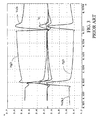
Figure 2 operates in a way similar to the previous situation. However, this time the charge sharing occurs between the two upper capacities, connected to the nodes VcU(i-1) and vcU(i). - it is to be noted that during the two semi-periods in which the nodes PgD, PgU, NgD, NgU, go high or low, they remain for the whole time of the sharing always constant, and at such a voltage as to allow an efficient turn-on and turn-off of the pass transistors connected thereto, also when the supply voltage Vdd is equal to IV, as shown in
Figure 3 . In particular,Figure 3 shows the semi-period in which the charge sharing occurs between the two bottom capacities, i.e. the capacities connected to the nodes VcD(i-1) and VcD(i). - The transistors Mp1 and Mp2, Mn1, Mn2 allow the capacities Cb to update at the voltage they refer to and to recover that charge lost to drive the pass transistors.
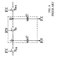
- To completely evaluate the characteristics of this known circuit, let's evaluate the differences of potential between the various nodes. Let's consider the voltage differences between the nodes of a generic stage j of the single charge pump latch circuit, as shown in
Figure 4 or equivalently of one of the charge pump stages of the circuit shown inFigure 2 . - Let's start from the most intuitive condition, which is that of end sharing ("End Sharing" instant -
Fig. 4 ), when the voltage difference between the nodes A and B is obviously void:
- During the sharing, the voltage at the node A has been reduced by ΔV, being:

- while that at the node B increases by the same amount, thus at the beginning of the sharing there occurs:

- But let's go back to the end sharing instant, at this point the phases switch ("Start No Sharing" instant) and, in consequence, the voltage at the node A decreases by a value equal to the supply voltage Vdd, while that at the node B increases by the same amount. This implies:

- During this semi-period there is no sharing in the stage j, while it is present in the adjacent stages, thus the capacity at the node A receives charge from that of the previous stage and the capacity at the node B transfer charge to that of the successive stage. At the end of the semi-period ("End No Sharing" instant) the voltage at the node A has increased by ΔV while that at the node B has been reduced by ΔV, thus there occurs:

- The results so far obtained are summarised in the following table:
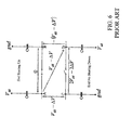
Table 1 VAB End_Sh = 0End sharing between A and B VAB Start_NoSh = 2VddStart no sharing between A and B VAB Endt_NoSh = 2Vdd-2ΔVEnd no sharing between A and B VAB Start_Sh = 2ΔVStart sharing between A and B - Let's now reconsider a double charge pump circuit, making reference to the schemes of
Figures 5 and6 . In particular, the circuit schematically comprises two upper nodes A and B and two lower nodes C and D whereto respective capacities are connected. It is immediate to verify that the differences of potential between the nodes during the operation are the following ones: - under the Start Sharing Up and Start No Sharing Down conditions of
Figure 5 :
- under the End Sharing Up and End No Sharing Down conditions of
Figure 6 :
- Considering then the circuit complete with the switches as shown in
Figure 2 , the absolute values of the voltages at the nodes at the end of the semi-period in which the charge sharing has occurred between the two bottom capacities are summarised in the following table:Table 2 V CUi-1 Vi - Vdd + ΔV V CDi-1 Vi VCUi Vi + Vdd - ΔV VCDi Vi PgD Vi - Vdd PgU Vi NgD Vi + Vdd NgU Vi - Therefore, observing the differences of potential, the two pass transistors MpD and MnD on the bottom of
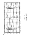
Figure 2 are on while those MpU and MnU on top are off. It is to be noted that, given the difficulty of obtaining perfectly crossed phases of the charge pump circuit, they are preferably realised overlapped or disoverlapped. In fact, when the phases are overlapped i.e. when both FX and FN are equal to Vdd, the values of the voltages at the nodes become:Table 3 V CUi-1 Vi + ΔV V CDi-1 Vi VCUi Vi + Vdd - ΔV VCDi Vi + Vdd PgD Vi PgU Vi NgD Vi + Vdd NgU Vi + Vdd - It results that the pass transistor MpU is on, but also the transistors Mn1 and Mn2 are on. In consequence, the capacities Cb which drive the N-channel MOS transistors are unloaded on the pumping capacity C and in a different way with respect to each other. This creates an asymmetry of the potentials at the nodes between the high part of the charge pump circuit and the low one during the charge sharing phases, as graphically shown in
Figure 7 . - The technical problem of the present invention is that of overcoming the limits of the solutions currently proposed by the prior art obtaining a charge pump latch circuit able to work correctly also at very low supply voltages.
- The solution idea underlying the invention is that of managing the phases of the stabilisation stage of the charge pump circuit so as to turn off all the four pass transistors during the overlapping of the phases themselves, avoiding in this way asymmetries of potential during the phases of charge sharing. In particular, advantageously according to the invention, the phases FX and FN which drive portions of the
stabilisation stage 20 connected to successive charge pump stages are inverted in a portion with respect to the other. Further advantageously, in an embodiment of the circuit according to the invention, the phases are negated and suitably shifted to avoid any problem of stress on the thin oxide layers of the gate terminals of the transistors of the charge pump circuit during the charge sharing phases. - On the basis of this solution idea the technical problem is solved by a charge pump latch circuit of the type previously indicated and characterised in that the stabilisation stage is connected to at least one first and one second pair of first and second enable terminals receiving suitable and distinct phase signals able to ensure the turn-off of said stabilisation stage during the overlapping periods of said phase signals.
- The problem is also solved by a method for driving transistors comprised in a first and a second charge pump stage by means of a stabilisation stage connected to control terminals of said transistors and suitable to ensure the turn-off of this stabilisation stage during the overlapping periods of the relative phase signals.
- The characteristics and the advantages of the circuit and of the method according to the invention will be apparent from the following description of an embodiment thereof given by way of indicative and non limiting example with reference to the annexed drawings.
- In these drawings:
-
Figures 1 and2 schematically show a charge pump circuit of the latch type realised according to the prior art; -
Figure 3 shows the trend of inner signals of the charge pump circuit ofFigure 2 ; -
Figures 4 ,5 and6 show functional schematisations of the circuit ofFigure 2 ; -
Figure 7 shows the trend of inner signals of the circuit ofFigure 2 ; -
Figure 8 schematically shows a charge pump circuit realised according to the invention; -
Figure 9 shows in greater detail a detail of the circuit ofFigure 8 during a charge sharing phase; -
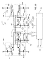
Figure 10 schematically shows an alternative embodiment of the charge pump circuit realised according to the invention; -
Figures 11 and 12 show respective schematic views of circuits generators of phases used in the alternative embodiment of the circuit ofFigure 10 ; -
Figure 13A shows the trend of signals of are applied to the circuit ofFigure 10 ; -
Figure 13B shows the trend of signals applied at the input of the circuits ofFigures 11 and 12 ; -
Figure 14 shows the trend of inner signals of the circuit ofFigure 10 . - The invention will be now described in detail with particular reference to the example of
Figure 8 , which shows a chargepump latch circuit 10 comprising at least two charge pump stages, a generic charge pump stage being indicated as CBj. - The
latch circuit 10 comprises several components which will be now described by identifying their belonging to functional blocks indicated inside dotted lines inFigure 8 . - We will start from a first stage CBi-1 we can defined input stage, even if, in reality, it can be considered a generic stage of the charge
pump latch circuit 10. - This first stage CBi-1 comprises a first latch circuit Li-1, inserted between a first CUpi-1 and a second inner circuit node CDowni-1 and connected to an intermediate circuit node INT. The first latch circuit Li-1 comprises suitable transistors having the function of switch or pass transistor, in particular a first and a second transistor, MpU and MpD, in the example shown of the MOS type with P channel.
- The successive or consecutive stage CBi comprises a second latch circuit Li, inserted between a third CUpi and a fourth inner circuit node CDowni and connected to the intermediate circuit node INT. The second latch circuit Li similarly comprises suitable transistors having the function of switch or pass transistor, in particular a third and a fourth transistor, MnU and MnD, in the example shown of the MOS type with N channel. This successive stage will be described hereafter also as second stage or output stage.
- The charge
pump latch circuit 10 also comprises astabilisation stage 20 connected to the intermediate circuit node INT. Advantageously according to the invention, thestabilisation stage 20 is also connected to at least one first CFO1 and one second pair CFO2 of first and second enable terminals receiving suitable phase signals and it is connected to control terminals or gates of the transistors of the latch circuits Lj inside the charge pump stages CBj. - In other words, the charge
pump latch circuit 10 according to the invention comprises a plurality of charge pump stages CBj inserted in series to each other between a first and second enable terminals receiving suitable phase signals, FX and FN, interconnected pairs, in particular consecutive, of these charge pump stages, CBi-1 and CBi, being connected to an intermediate circuit node INT. The chargepump latch circuit 10 according to the invention also comprises astabilisation stage 20 connected to the intermediate circuit node INT and to control terminals of transistors inside the charge pump stages, CBi-1 and CBi. Advantageously according to the invention, thestabilisation stage 20 is also connected to at least one first and one second pair of first and second enable terminals receiving suitable and distinct phase signals, to ensure the turn-off of thestabilisation stage 20, in particular of all the transistors comprised therein, i.e. the transistors Mp1, Mp2, Mn1, Mn2, during the overlapping periods of these phase signals. - In particular, advantageously according to the invention, the
latch circuit 10 thus comprises aphase generator 25 suitable to supply thestabilisation stage 20 with these suitable and distinct phase values. Thephase generator 25 has a pair of input terminals CFI receiving a first and a second input signal, FA and FB, as well as a first pair CFO1 and a second pair CFO2 of output terminals respectively connected to the first and second pairs of enable terminals of thestabilisation stage 20, always indicated as CFO1 and CFO2. - Suitably, the
stabilisation stage 20 comprises at least one first 22p and onesecond biasing portion 22n, respectively connected to the first and to the second charge pump stage, CBi-1 and CBi, in particular to control terminals of transistors comprised therein, as well as to the first and to the second pair of output terminals, CFO1 and CFO2, of thephase generator 25 for receiving therefrom the suitable and distinct phase signals, in particular the phases FX and FN and their negated values FXN and FNN. - More in particular, the
stabilisation stage 20 comprises, in reality, a plurality of stabilisation stages, connected between pairs of consecutive charge pump stages, a single stabilisation stage being shown inFigure 8 since it shows, for sake of simplicity, only two charge pump stages CBi-1 and CBi, this stage being indicated however with thereference 20. - Suitably, in each
stabilisation stage 20, the first 22p and thesecond biasing portion 22n are connected to the transistors of the latch circuits Lj of the charge pump stages. In particular, thefirst biasing portion 22p is connected to the first latch circuit Li-1 of the first stage or input stage CBi-1 and to the first pair CFO1 of enable terminals. Similarly, thesecond biasing portion 22n is connected to the second latch circuit Li of the second stage or output stage CBi and to the second pair CFO2 of enable terminals. - In particular, the
first biasing portion 22p comprises: - a first biasing capacitor Cbp1, inserted between a first control terminal PgU and a second enable terminal FN of the first pair CFO1 of enable terminals;
- a second biasing capacitor Cbp2, inserted between a second control terminal PgD and a first enable terminal FX of the first pair of enable terminals CFO1;
- a first control transistor Mp1, inserted between the intermediate circuit node INT and the first control terminal PgU and having a control terminal or gate connected to the second control terminal PgD; and
- a second control transistor Mp2, inserted between the intermediate circuit node INT and the second control terminal PgD and having a control terminal or gate connected to the first control terminal PgU.
- In a similar way, the
second biasing portion 22n comprises: - a third biasing capacitor Cbn1 inserted between a third control terminal NgU and a first enable terminal FXN of the second pair CFO2 of enable terminals;
- a fourth biasing capacitor Cbp2 inserted between a fourth control terminal NgD and a second enable terminal FNN of the second pair CFO2 of enable terminals;
- a third control transistor Mn1, inserted between the intermediate circuit node INT and the third control terminal NgU and having a control terminal or gate connected to the fourth control terminal NgD; and
- a fourth control transistor Mn2, inserted between the intermediate circuit node INT and the fourth control terminal NgD and having a control terminal or gate connected to the third control terminal NgU.
- Suitably, the first and second control transistors, Mp1 and Mp2, are of the same type as that of the first and second transistors, MpU and MpD, of the first latch circuit Li-1 of the first charge pump stage CBi-1, i.e. they are P-channel MOS transistors, while the third and the fourth control transistor, Mn1 and Mn2, are of the same type as that of the third and fourth transistor, MnU and MnD, of the second latch circuit Li of the second charge pump stage CBi, i.e. they are N-channel MOS transistor.
- The voltage signal Vint at the intermediate circuit node INT remains constant and is used for correctly driving the turn-on and the turn-off of the latch transistors or pass transistors MpU, MpD, MnU, MnP.
- VcU and VcD indicate the voltage signals at the nodes Up and Down, respectively, of each charge pump stage CB. Moreover, also in this case the phases FX and FN, respectively FXN and FNN, are, at any time, complementary to each other.
- It is possible to distinguish two different operative conditions equivalent to each other:
- FN=Vdd , FX=0 (FNN=0, FXN=Vdd), VcDi-1 is brought high and VcUi-1 is brought low, VcDi is low while VcUi is high. In this case, the node PgU is brought high (to a value equal to Vint) while the node PgD is brought low (in particular, by an amount equal to Vdd with respect to Vint), thus allowing to turn on the transistor MpD and to turn off the transistor MpU.
- In the same semi-period, the node NgD is brought high (by an amount equal to Vdd with respect to Vint) and the node NgU is brought low. Then the transistor MnD is turned on, while the transistor MnU is turned off. In this way the charge sharing is obtained between the two adjacent pump capacitors connected to the terminals Downi-1 and Downi, while it is prevented between the two adjacent pump capacitors connected to the terminals Upi-1 and Upi,
- FN=0, FX =Vdd (FNN=Vdd, FXN=0); in this case the charge
pump latch circuit 10 operates in a similar although dual way with respect to the previous situation. - It is to be noted that, advantageously according to the invention, during the two semi-periods in which the nodes PgD, PgU, NgD, NgU go high or low, they remain for the whole time of the charge sharing always constant, and at such a voltage as to allow an efficient turn-on and turn-off of the transistors comprised in the latch circuits connected thereto.
- More in detail, to understand the operation of the charge
pump latch circuit 10 according to the invention, the start of a charge sharing step between the pump capacitors connected to the nodes Up of the charge pump stages is considered, thus with the first phase FX at Vdd and the second phase FN at zero. - In this period, the latch transistors connected to the nodes Up, i.e. the first transistor MpU and the third transistor MnU, should be well on while those connected to the nodes Down, i.e. the second transistor MpD and the fourth transistor MnD, well off so as not to favour any charge return.
- It is important to note that the
stabilisation stage 20 of the chargepump latch circuit 10 generates potentials capable of driving in a very efficient way the control terminals of the latch transistors, also during the whole charge sharing period. - In fact, during this charge sharing period, the potentials thus obtained remain constant.
- In particular, considering the above reported charge sharing condition of the capacitors connected to the nodes Up, it occurs that, at the beginning of the charge sharing period, when the phase FX is brought to Vdd, the node PgD, which was previously at Vint-Vdd now increases and is brought to Vint. This value leads to the turn-off of the second latch transistor MpD as well as of the first control transistor Mp1.
- As regards the node PgU, in the previous period it was brought to Vint while now, since the phase FN has decreased to zero, is brought to Vint-Vdd. This value leads to the turn-on of the first latch transistor MpU as well as of the second control transistor Mp2.
- In substance, the control transistors, Mp1 and Mp2, respectively Mn1 and Mn2, comprised in the
stabilisation stage 20, allow the respective biasing capacitors, Cbp1 and Cbp2, respectively Cbn1 and Cbn2, to update with respect to the voltage on the node they refer to and to recover the lost charge to correctly drive the latch transistors. - In this way, the charge
pump latch circuit 10 according to the invention correctly operates also for supply voltages Vdd having a value next to the threshold voltage value of the transistors, in particular equal to 1V. - The output current-voltage characteristic of the charge
pump latch circuit 10, thanks to thestabilisation stage 20, remarkably improves with respect to the solutions of the prior art and follows a linear law. - However, the most delicate part of the circuit is represented by the difficulty found in the generation of the phases FX and FN so that they are perfectly crossed with each other.
- It occurs, in fact that these phases FX and FN are overlapped for an overlapped period Δt.
- Thus, when the first phase FX is brought to a high value, equal to the supply voltage Vdd, the charge sharing period of the pump capacitors connected to the nodes Up should start.
- Unfortunately, due to the delay with which the second phase FN is brought to a low value, in particular to the ground potential, a correct charge sharing is not obtained since the transistors of the latch circuits of the charge pump stages during the overlapping period Δt are not under correct conditions for the charge sharing and in particular they are all under the turn-off conditions.
- Under these conditions, there is no passage of charge from the pump capacitor CUpi-1 connected to the node Upi-1 to the pump capacitor CUpi connected to the node Upi, as desired, while from the pump capacitor CDowni connected to the node Downi and from the biasing capacitors, Cbn1 and Cbn2, connected to the nodes NgU and NgD, respectively, to the pump capacitor CUpi connected to the node Upi.
- This pump capacitor CUpi thus receives more charge than the charge received by the pump capacitor CDowni connected to the node Downi in the successive period and thus this behaviour leads to an asymmetry in the charge sharing.
- The invention also solves this potential drawback providing the use of suitable and distinct phase signals, in particular of the phases FX and FN and of their negated values FXN and FNN applied to distinct pairs of enable terminals of the
stabilisation stage 20. - Thanks to this measure the negated phases FXN and FNN turn off all the four switches, i.e. the control transistors Mp1, Mp2, Mn1, Mn2, during the overlapping period.
- In particular, advantageously according to the invention, the
latch circuit 10 thus comprises thephase generator 25. - In a first embodiment of the
latch circuit 10 according to the invention, thephase generator 25 essentially comprises a first inverter INV1 and a second logic inverter INV2 connected to the pair of input terminals CFI which already receive the phases FX and FN. These inverters INV1 and INV2 are also connected to the second pair CFO2 of enable terminals to apply to them the negated phases FXN and FNN, while the first pair CFO1 of enable terminals is simply connected directly to the pair of input terminals CFI for receiving the phases FX and FN. - In the example shown in
Figure 8 , these inverters INV1 and INV2 are thus placed upstream of the biasing capacitors, Cbn1 and Cbn2, of theportion 22n of thestabilisation stage 20. - In particular, the third biasing capacitor Cbn1 is connected, through the first inverter INV1, to the first enable terminal FN and then receives the signal FNN complementary to the first phase FN.
- The fourth biasing capacitor Cbn2 is connected, through the second inverter INV2, to the first enable terminal FX and then receives the signal FXN complementary to the first phase FX.
- In this way, the third and fourth control transistors, Mn1 and Mn2, suitably driven by the complementary values FNN and FXN of the phases FX and FN, remain off during the overlapping period At, thus forcing under the turning-off condition also the fourth latch transistor MnD.
- It is important to note that in this way, advantageously according to the invention, a correct charge sharing is ensured, also if the turn-on of the first and third latch transistor, MpU and MnU, only occurs after the end of the overlapping period At thus reducing the sharing period, without however introducing particular drawbacks for the operation of the charge
pump latch circuit 10. - The circuit configuration of
figure 8 also solves possible problems linked to the disoverlapping case. - In fact, it is immediate to verify that the situation previously indicated with reference to the phases in overlapping is proposed again also in case of disoverlapping of the phases FX and FN, although this situation can interest only the control transistors Mp1 and Mp2 of the
first portion 22p of thestabilisation stage 20. - Simulations carried out on the charge
pump latch circuit 10 shown inFigure 8 clarify how each asymmetry problem in the charge sharing is solved. - The control terminals of the transistors contained in the charge
pump latch circuit 10 are correctly biased for the whole duration of the semi-periods in which the charge sharings occur. This allows to maintain the sizes of the charge pump stages reduced so as to meet the specifications, in fact it allows to size them according to the mathematical law characterising its typical behaviour. - During the overlapping of the phases, i.e. when FX=FN=VDD, the transistors Mn1 and Mn2 are off and prevent the two capacities Cbn1 and Cbn2 connected thereto from losing charge. Moreover, to turn on and off the pass transistors it is enough to supply their gates with such a biasing voltage as the gate-source voltage, in absolute value, |Vgs| is smaller at the beginning of the semi-period and maximum immediately after.
- In substance, the
phase generator 25 of the chargepump latch circuit 10 according to the invention allows to obtain suitable and distinct phase signals to be applied to the first and second pairs of enable terminals, CFO1 and CFO2, of thestabilisation stage 20 to turn off all control transistors comprised therein prior to the charge sharing step. - Further advantageously according to the invention,
Figure 10 shows an alternative embodiment of the chargepump latch circuit 10 according to the invention. - In particular, according to this alternative embodiment, the charge
pump latch circuit 10 according to the invention receives in correspondence with the second pair CFO2 of enable terminals shifted phases FX_SHIFT and FN_SHIFT negated and suitable level shifted with respect to the phases FX and FN supplied on the first pair CFO1 of enable terminals, these suitably shifted phases being generated by thephase generator 25 starting from suitable input signals FA and FB. - In fact, it is easily understood that a simple inversion of the phases FX and FN operated by the
phase generator 25 comprised in the chargepump latch circuit 10 ofFigure 8 if, on one side, allows to eliminate the problem of the potential asymmetries in the charge sharing periods, on the other introduces a potential stress problem on the oxides of the low voltage pass transistors during these charge sharing periods. - In fact, let's consider the charge
pump latch circuit 10 shown inFigure 8 and a cycle in which the first phase FX is low (FX=0) and the second phase FN is high (FN=Vdd). In this hypothesis, it occurs that:
- When the phase overlapping occurs (with FX high and FN high) all the pass transistors of the charge
pump latch circuit 10 result - as desired - off and it occurs that:
- Subsequently, the second phase FN is brought low and the charge sharing step starts. In this time range, as schematically shown in
Figure 9 , it occurs that the buffers INV1 and INV2 which generate the negated phases FXN and FNN supply a lot of current in the initial part of this charge sharing. In particular, these buffers INV1 and INV2 comprise respective first and second MOS transistor. The first buffer INV1 comprises a first P-channel MOS transistor, Mpb1, and a second N-channel MOS transistor, Mnb1, inserted in series to each other between the supply reference Vdd and the ground GND and having gate terminals connected to each other and receiving the second phase FN, as well as an intermediate circuit node suitable for realising the output terminal of the buffer and for supplying the biasing capacitor Cbn1 connected thereto with the second negated phase FNN. Similarly, the second buffer INV2 comprises a first P-channel MOS transistor, Mpb2, and a second N-channel MOS transistor, Mnb2, inserted in series to each other between the supply reference Vdd and the ground GND and having gate terminals connected to each other and receiving the first phase FX, as well as an intermediate circuit node suitable for realising the output terminal of the buffer and for supplying the biasing capacitor Cbn2 connected thereto with the first negated phase FXN. - In consequence, a resistive drop on the transistors Mnb1-Mnb2 and Mpb1-Mpb2 comprised in these buffers INV1 and INV2 limits the voltage on the gate terminals of the pass transistors with P channel (in this case the pass transistor MpU in
Figure 8 ). - It thus occurs that, in the initial phase of the charge sharing, the voltage between the node VcUi-1 (corresponding to the source terminal of the pass transistor MpU) and the node PgU (corresponding to the gate terminal of the pass transistor MpU) is given by:

- ΔVnb and ΔVpb being the voltage drops on the transistors with N channel and with P channel, respectively, of the buffers INV1 and INV2. In particular, in the case shown in
Figure 9 where the second phase FN is low and the first phase FX is high, ΔVnb is the drop of potential across the transistor Mnb1 of the first buffer INV1 and ΔVpb is the drop of potential across the transistor Mnp2 of the second buffer INV2. - In other words, the overall voltage drop ΔVnb+ΔVpb limits the source-gate voltage Vsg of the pass transistor with P channel MpU. It is to be noted in fact that in the absence of the transistors of the buffers INV1 and INV2 the source-gate voltage value of this transistor MpU would be greater than the supply voltage value and equal to Vsg = (Vdd+ ΔV).
- This mechanism does not act however on the pass transistor with N channel MnU for which the source-gate voltage Vsg is equal to ΔV+Vdd-ΔVnb.
- It then occurs that the initial voltage on the gate terminal of this pass transistor with N channel, MnU, is higher than that on the gate terminal of the pass transistor with P channel, MpU, with subsequent risk of breakage of the gate terminal (in particular of the gate oxide layer) of the pass transistor with N channel, MnU.
- Advantageously according to this alternative embodiment of the invention, the
phase generator 25 supplies thestabilisation stage 20 with shifted phases FX_SHIFT and FN_SHIFT negated and suitably level shifted with respect to the phases FX and FN supplied to the first pair CFO1 of enable terminals. - In particular, to overcome the above indicated drawbacks, the shifted phases FX_SHIFT and FN_SHIFT are overlapped to offer such a transient resistive drop as to protect against overvoltages, i.e. against voltages higher than the maximum value given by the value of the supply voltage Vdd, the gate terminals of the pass transistor of the charge
pump latch circuit 10. - For this specific purpose the alternative embodiment shown in
Figure 10 uses respective digitallevel shifter circuits stabilisation stage 20 respective shifted phase signals FX_SHIFT and FN_SHIFT negated and level shifted. - The
circuit 30 is shown inFigure 11 , while thecircuit 40 is shown inFigure 12 . - In particular, the
circuits - The
circuit 30 comprises a firstinput circuit portion 35 with transistors inserted between the supply reference Vdd and the ground GND in which an output stage with a complementary pair of transistors Mp3, Mn3 produces the first phase signal FX starting from a first input signal FA. This first phase signal FX is applied to a conduction terminal of an output circuit portion comprising a further complementary pair of transistors Mp5, Mn5 which receive on their own common control terminals a second input signal FB. - The body terminal of the pull up transistor Mp5 of the further complementary pair of transistors Mp5, Mn5 is biased at the value of the supply voltage Vdd.
- At the output of the further complementary pair of transistors Mp5, Mn5 the first shifted phase signal FX_SHIFT is generated, negated and suitably level shifted with respect to the first phase signal FX.
- Similarly, the
circuit 40 comprises a firstinput circuit portion 45 with transistors inserted between the supply reference Vdd and the ground GND in which an output stage with a complementary pair of transistors Mp4, Mn4 produces the second phase signal FN starting from the second input signal FB. This second phase signal FN is applied to a conduction terminal of an output circuit portion comprising a further complementary pair of transistors Mp6, Mn6 which receive on their own common control terminals the first input signal FA. - The body terminal of the pull up transistor Mp6 of the further complementary pair of transistors Mp6, Mn6 is biased at the supply voltage value Vdd.
- At the output of the further complementary pair of transistors Mp6, Mn6 the second shifted' phase signal FN_SHIFT is generated, negated and suitably level shifted with respect to the second phase signal FN.
- The trend of the input signals FA and FB is shown in
Figure 13B , whileFigure 13A shows the trend of the phase signals FX and FX and of the shifted phase signals FX_SHIFT and FN_SHIFT. - Going back to the charge
pump latch circuit 10 ofFigure 10 , during the previously analysed overlapping phase the two phases FX and FN are high (Vdd) and in consequence the PMOS switches are off while the shifted phases FX_SHIFT and FN_SHIFT are low (GND) and the two NMOS switches are off, exactly as desired. - Moreover, by sizing the PMOS transistors Mp3 and Mp4, Mp5 and Mp6 of the
circuits stabilisation stage 20 and avoiding stresses on the oxides of the pass transistors of the chargepump latch circuits 10. - In this way it is possible to obtain a smaller |Vgs| at the beginning of the charge sharing semi-period and a greater one during the charge sharing until the end of the semi-period.
- This situation is shown by the trend of the signals reported in
Figure 14 . - It should also be underlined that in a real circuit the well known body effect is to be taken into account, this effect tending to increase the threshold voltage of the transistors, reducing the potentialities of the charge pump circuit.
- Moreover, considering that PMOS transistors have been used as pass transistors for the charge sharing between the charge pump stages CBi, in particular the transistors MpU and MpD, the so called latchup phenomenon is also to be taken into account, being triggered by the parasite transistors due to the junctions pnpn contained in the CMOS structures like the latch circuits Li.
- These measures are however well known by the technician of the field who will take care of balancing the
circuits - Advantageously according to the invention, the charge
pump latch circuit 10 as proposed shows the following fundamental advantages: - It does not suffer from asymmetries since the phase signals FX and FN and their negated values FXN and FNN turn off all the pass transistors prior to the charge sharing;
- It allows to protect the gate terminals (in particular the thin oxide layers) of the low voltage (LV) transistors thanks to the generation of negated and suitably shifted phases (FX_SHIFT, FN_SHIFT) which avoid, by virtue of the resistive drops on the output terminals of the level shifter circuits which generate these phases, during the transients of the charge sharing phases, the overvoltages which would otherwise damage these LV transistors.
- The invention also relates to a method for driving transistors comprised in a first and a second charge pump stage, CBi-1, CBi, interconnected in the intermediate circuit node INT, by means of the
stabilisation stage 20 connected to control terminals of these transistors. Advantageously, the method comprises a generation step, by thestabilisation stage 20, of at least one first pair of phase signals and a second pair of phase signals and a step of applying to a first and a second pair of enable terminals, CFO1 and CFO2, of thestabilisation stage 20 the first and second pair of phase signals to ensure the turn-off of thestabilisation stage 20 itself during the overlapping periods of these phase signals. - Further, this step of generating pairs of phase signals allows to obtain the second pair of phase signals, FXN and FNN, negated with respect to the first pair of phase signals, FX and FN.
- Alternatively, this step of generating pairs of phase signals allows to obtain the second pair of phase signals, FXN_SHIFT and FNN_SHIFT, negated and suitably level shifted with respect to the first pair of phase signals, FX and FN.
- The invention allows to remarkably improve the functionality of the charge pump latch circuits thanks to the difference way of generating the phases. In this way, any possible bad operation due to the charge sharing of the capacities Cb with the pumping capacity is prevented.
- Moreover, by suitably sizing the
circuits
Claims (16)
- Charge pump latch circuit (10) comprising at least one first and one second charge pump stage (CBi-1, CBi) interconnected in an intermediate circuit node (INT) and a stabilisation stage (20) connected to said intermediate circuit node (INT) and to control terminals of transistors comprised in said first and second charge pump stages (CBi-1, CBi) characterised in that said stabilisation stage (20) is connected to at least one first and one second pair (CFO1, CFO2) of first and second enable terminals receiving suitable and distinct phase signals able to ensure the turn-off of said stabilisation stage (20) during the overlapping periods of said phase signals.
- Charge pump latch circuit (10) according to claim 1, characterised in that it comprises a phase generator (25) having at least one pair of input terminals (CFI) receiving a first and a second input signal (FA, FB), as well as a first and a second pair (CFO1, CF02) of output terminals respectively connected to said first and second pair of enable terminals (CFO1, CFO2) of said stabilisation stage (20) to supply them with said suitable and distinct phase signals.
- Charge pump latch circuit (10) according to claim 2, characterised in that said stabilisation stage (20) comprises at least one first and one second biasing portion (22p, 22n), respectively connected to said first and second charge pump stages (CBi-1, CBi), in particular to control terminals of transistors comprised therein, as well as to said first and second pair of output terminals (CFO1, CFO2) of said phase generator (25) to receive therefrom said suitable and distinct phase signals.
- Charge pump latch circuit (10) according to claim 3, characterised in that said phase generator circuit (25) comprises at least one first and one second inverter (INV1, INV2) connected, between said pair of input terminals (CFI) receiving a first pair of a first and a second phase signal (FX, FN) and said second pair of enable terminals (CFO2), to apply a second pair of a first and a second negated phase signal (FNN, FXN) to said second pair of enable terminals (CFO2), said first pair of enable terminals (CFO1) being directly connected to said pair of input terminals (CFI) and receiving said first pair of phase signals (FX, FN).
- Charge pump latch circuit (10) according to claim 4, characterised in that:- said first buffer (INV1) comprises a first and a second transistor (Mpb1, Mnb1), inserted in series to each other between said first and second voltage references (Vdd, GND) and having control terminals connected to each other and receiving said second phase signal (FN), as well as an intermediate circuit node suitable for realising an output terminal of said first buffer (INV1) and for supplying a biasing capacitor (Cbn1) connected thereto with said second negated phase signal (FNN); and- said second buffer (INV2) comprises a first and a second transistor (Mpb2, Mnb2), inserted in series to each other between said first and second voltage references (Vdd, GND) and having control terminals connected to each other and receiving said first phase signal (FX), as well as an intermediate circuit node suitable for realising an output terminal of said second buffer (INV2) and for supplying a biasing capacitor (Cbn2) connected thereto with said first negated phase signal (FXN).
- Charge pump latch circuit (10) according to claim 4, characterised in that said phase generator circuit (25) further comprises respective phase generator circuits (30, 40) which are also level shifters for supplying said second pair of phase signals negated and suitably level shifted (FX_SHIFT, FN_SHIFT) with respect to said first pair of phase signals (FX, FN).
- Charge pump latch circuit (10) according to claim 6, characterised in that each phase generator circuit (30, 40) and level shifter comprises an input circuit portion (35, 45) for generating a phase signal (FX, FN) of said first pair of phase signals starting from an input signal (FA, FB) and an output circuit portion for generating a phase signal (FX_SHIIFT, FN_SHIFT) of said second pair of phase signals, negated and level shifted with respect to the respective phase signal (FX, FN).
- Charge pump latch circuit (10) according to claim 7, characterised in that each of said output circuit portions comprises a complementary pair of transistors (Mp5, Mn5; Mp6, Mn6) receiving on a respective conduction terminal one of said phase signals (FX, FN).
- Charge pump latch circuit (10) according to claim 3, wherein each charge pump stage (CBi-1, CBi) comprises:- a first pump capacitor (CUpi-1, CUpi) inserted between a first and a second enable terminal (FX, FN) and a first inner cricuit node (Upi-1, Upi);- a second pump capacitor (CDowni-1, CDowni) inserted between said second and said first enable terminal (FX, FN) and a second inner circuit node (Downi-1, Downi); as well as- latch transistors (MpU, MnU; MpD, MnD) inserted between said first and second inner circuit nodes (Upi-1, Upi; Downi-1, Downi) and said intermediate circuit node (INT),
said first and second enable terminals (FX, FN) receiving respective phase signals (FX, FN), complementary to each other,
characterised in that:
said first biasing portion (22p) is connected to said control terminals (PgU, PgD) if said first and second latch transistors (MpU, MpD) of said first charge pump stage (CBi-1) and to said first pair of enable terminals (CFO1) and
said second biasing portion (22n) is connected to said control terminals (NgU, NgD) of said first and second latch transistors (MnU, MnD) of said second charge pump stage (CBi) and to said second pair of enable terminals (CFO2). - Charge pump latch circuit (10) according to claim 9, characterised in that said first and second biasing portion (22p; 22n) comprise:- respective first biasing capacitors (Cbp1, Cbn1) inserted between said control terminals (PgU, NgU) of said first latch transistors (MpU, MnU) of said charge pump stages (CBi-1, CBi) and corresponding second enable terminals (FN; FNN) of said first and second pairs of enable terminals (CFO1, CFO2), respectively; and- respective second biasing capacitors (Cbp2, Cbn2) inserted between said control terminals (PgD, NgD) of said second latch transistors (MpD, MnD) of said charge pump stages (CBi-1, CBi) and corresponding first enable terminals (FX; FXN) of said first and second pairs of enable terminals (CFO1, CFO2), respectively.
- Charge pump latch circuit (10) according to claim 10, characterised in that said first and second biasing portions (22p; 22n) further comprise:- respective first control transistors (Mp1, Mn1), inserted between said intermediate circuit node (INT) and between said control terminals (PgU, NgU) of said first latch transistors (MpU, MnU) of said charge pump stages (CBi-1, CBi) and having respective control terminals connected to said control terminals (PgD, NgD) of said second latch transistors (MpD, MnD) of said charge pump stages (CBi-1, CBi); and- respective second control transistors (Mp2, Mn2), inserted between said intermediate circuit node (INT) and said control terminals (PgD, NgD) of said second latch transistors (MpD, MnD) of said charge pump stages (CBi-1, CBi) and having respective control terminals connected to said control terminals (PgU, NgU) of said first latch transistors (MpU, MnU) of said charge pump stages (CBi-1, CBi).
- Charge pump latch circuit (10) according to claim 11, characterised in that said control transistors (Mp1, Mp2; Mn1, Mn2) are of the same type as said latch transistors (MpU, MpD; MnU, MnD).
- Charge pump latch circuit (10) according to any of the preceding claims, characterised in that it comprises a plurality of charge pump stages (CB) and in that said stabilisation stage (20) comprises a plurality of stabilisation stages, each stabilisation stage (20) being inserted between pairs of charge pump stages interconnected to each other of said charge pump latch circuit (10).
- Method for driving transistors comprised in a first and a second charge pump stage (CBi-1, CBi), interconnected in an intermediate circuit node (INT), by means of a stabilisation stage (20) connected to control terminals of said transistors, characterised in that it comprises a generation step by said stabilisation stage (20) of at least one first pair of phase signals and one second pair of phase signals and a step of applying to a first and to a second pair of enable terminals (CFO1, CFO2) of said stabilisation stage (20) said first and second pairs of phase signals to ensure the turn-off of said stabilisation stage (20) during the overlapping periods of said phase signals.
- Method according to claim 14, characterised in that said generation step of pairs of phase signals allows to obtain said second pair of phase signals (FXN, FNN) negated with respect to said first pair of phase signals (FX, FN).
- Method according to claim 14, characterised in that said generation step of pairs of phase signals allows to obtain said second pair of phase signals (FXN_SHIFT, FNN_SHIFT), negated and suitably level shifted with respect to said first pair of phase signals (FX, FN).
Priority Applications (2)
| Application Number | Priority Date | Filing Date | Title |
|---|---|---|---|
| EP08425608.0A EP2166656B1 (en) | 2008-09-18 | 2008-09-18 | Electric circuit for generating low voltage and high frequency phases in a charge pump, in particular for supplies lower than 1V |
| US12/559,967 US8063693B2 (en) | 2008-09-18 | 2009-09-15 | Electronic circuit for generating low voltage and high frequency phases in a charge pump |
Applications Claiming Priority (1)
| Application Number | Priority Date | Filing Date | Title |
|---|---|---|---|
| EP08425608.0A EP2166656B1 (en) | 2008-09-18 | 2008-09-18 | Electric circuit for generating low voltage and high frequency phases in a charge pump, in particular for supplies lower than 1V |
Publications (2)
| Publication Number | Publication Date |
|---|---|
| EP2166656A1 true EP2166656A1 (en) | 2010-03-24 |
| EP2166656B1 EP2166656B1 (en) | 2013-04-10 |
Family
ID=40260734
Family Applications (1)
| Application Number | Title | Priority Date | Filing Date |
|---|---|---|---|
| EP08425608.0A Active EP2166656B1 (en) | 2008-09-18 | 2008-09-18 | Electric circuit for generating low voltage and high frequency phases in a charge pump, in particular for supplies lower than 1V |
Country Status (2)
| Country | Link |
|---|---|
| US (1) | US8063693B2 (en) |
| EP (1) | EP2166656B1 (en) |
Citations (3)
| Publication number | Priority date | Publication date | Assignee | Title |
|---|---|---|---|---|
| US20040239409A1 (en) * | 2003-05-28 | 2004-12-02 | Hynix Semiconductor Inc. | High voltage generator |
| US20060244516A1 (en) * | 2005-04-29 | 2006-11-02 | Hynix Semiconductor Inc. | Internal voltage generator |
| EP1881589A1 (en) * | 2006-07-19 | 2008-01-23 | STMicroelectronics S.r.l. | Charge pump circuit |
Family Cites Families (2)
| Publication number | Priority date | Publication date | Assignee | Title |
|---|---|---|---|---|
| JP3910765B2 (en) * | 1999-09-08 | 2007-04-25 | 株式会社東芝 | Voltage generation circuit and voltage transfer circuit using the same |
| JP3614747B2 (en) * | 2000-03-07 | 2005-01-26 | Necエレクトロニクス株式会社 | BOOST CIRCUIT, IC CARD WITH THE SAME AND ELECTRONIC DEVICE WITH THE SAME |
-
2008
- 2008-09-18 EP EP08425608.0A patent/EP2166656B1/en active Active
-
2009
- 2009-09-15 US US12/559,967 patent/US8063693B2/en active Active
Patent Citations (3)
| Publication number | Priority date | Publication date | Assignee | Title |
|---|---|---|---|---|
| US20040239409A1 (en) * | 2003-05-28 | 2004-12-02 | Hynix Semiconductor Inc. | High voltage generator |
| US20060244516A1 (en) * | 2005-04-29 | 2006-11-02 | Hynix Semiconductor Inc. | Internal voltage generator |
| EP1881589A1 (en) * | 2006-07-19 | 2008-01-23 | STMicroelectronics S.r.l. | Charge pump circuit |
Also Published As
| Publication number | Publication date |
|---|---|
| US8063693B2 (en) | 2011-11-22 |
| EP2166656B1 (en) | 2013-04-10 |
| US20100127760A1 (en) | 2010-05-27 |
Similar Documents
| Publication | Publication Date | Title |
|---|---|---|
| EP1881589A1 (en) | Charge pump circuit | |
| US4935644A (en) | Charge pump circuit having a boosted output signal | |
| US6501325B1 (en) | Low voltage supply higher efficiency cross-coupled high voltage charge pumps | |
| JP3554497B2 (en) | Charge pump circuit | |
| CN101170275B (en) | Charge pump circuit | |
| KR100684244B1 (en) | Charge pump circuit | |
| US20160006349A1 (en) | Four-phase charge pump circuit | |
| EP0813290B1 (en) | Multi-stage voltage-boosting circuit with boosted back-gate bias | |
| US20080143401A1 (en) | Charge pump circuit | |
| US10333397B2 (en) | Multi-stage charge pump circuit operating to simultaneously generate both a positive voltage and a negative voltage | |
| JPH02285959A (en) | Voltage multiplying circuit | |
| JP4849907B2 (en) | Charge pump circuit | |
| US5994949A (en) | Negative voltage charge pump particularly for flash EEPROM memories | |
| US9438103B2 (en) | Low voltage and high driving charge pump | |
| US20080246536A1 (en) | Two-phase charge pump circuit without body effect | |
| JPH1040680A (en) | Voltage pump circuit | |
| US6573780B2 (en) | Four-phase charge pump with lower peak current | |
| US5543668A (en) | Charge stacking on-chip high-voltage generator and method | |
| US7248096B2 (en) | Charge pump circuit with dynamic biasing of pass transistors | |
| JP4299857B2 (en) | Boost charge pump circuit | |
| US6046625A (en) | High current CMOS charge, particularly for flash EEPROM memories | |
| EP2166656B1 (en) | Electric circuit for generating low voltage and high frequency phases in a charge pump, in particular for supplies lower than 1V | |
| JPH11308856A (en) | Charge pump circuit device | |
| US7888970B1 (en) | Switch controlling circuit, switch circuit utilizing the switch controlling circuit and methods thereof | |
| KR100576812B1 (en) | Charge pump circuit and high voltage generation circuit |
Legal Events
| Date | Code | Title | Description |
|---|---|---|---|
| PUAI | Public reference made under article 153(3) epc to a published international application that has entered the european phase |
Free format text: ORIGINAL CODE: 0009012 |
|
| AK | Designated contracting states |
Kind code of ref document: A1 Designated state(s): AT BE BG CH CY CZ DE DK EE ES FI FR GB GR HR HU IE IS IT LI LT LU LV MC MT NL NO PL PT RO SE SI SK TR |
|
| AX | Request for extension of the european patent |
Extension state: AL BA MK RS |
|
| RAP1 | Party data changed (applicant data changed or rights of an application transferred) |
Owner name: STMICROELECTRONICS SRL |
|
| 17P | Request for examination filed |
Effective date: 20100922 |
|
| AKX | Designation fees paid |
Designated state(s): DE FR GB IT |
|
| 17Q | First examination report despatched |
Effective date: 20120328 |
|
| RAP1 | Party data changed (applicant data changed or rights of an application transferred) |
Owner name: STMICROELECTRONICS SRL |
|
| GRAP | Despatch of communication of intention to grant a patent |
Free format text: ORIGINAL CODE: EPIDOSNIGR1 |
|
| GRAS | Grant fee paid |
Free format text: ORIGINAL CODE: EPIDOSNIGR3 |
|
| GRAA | (expected) grant |
Free format text: ORIGINAL CODE: 0009210 |
|
| AK | Designated contracting states |
Kind code of ref document: B1 Designated state(s): DE FR GB IT |
|
| REG | Reference to a national code |
Ref country code: GB Ref legal event code: FG4D |
|
| REG | Reference to a national code |
Ref country code: DE Ref legal event code: R096 Ref document number: 602008023654 Country of ref document: DE Effective date: 20130606 |
|
| PLBE | No opposition filed within time limit |
Free format text: ORIGINAL CODE: 0009261 |
|
| STAA | Information on the status of an ep patent application or granted ep patent |
Free format text: STATUS: NO OPPOSITION FILED WITHIN TIME LIMIT |
|
| PG25 | Lapsed in a contracting state [announced via postgrant information from national office to epo] |
Ref country code: IT Free format text: LAPSE BECAUSE OF FAILURE TO SUBMIT A TRANSLATION OF THE DESCRIPTION OR TO PAY THE FEE WITHIN THE PRESCRIBED TIME-LIMIT Effective date: 20130410 |
|
| 26N | No opposition filed |
Effective date: 20140113 |
|
| REG | Reference to a national code |
Ref country code: DE Ref legal event code: R097 Ref document number: 602008023654 Country of ref document: DE Effective date: 20140113 |
|
| GBPC | Gb: european patent ceased through non-payment of renewal fee |
Effective date: 20130918 |
|
| PG25 | Lapsed in a contracting state [announced via postgrant information from national office to epo] |
Ref country code: GB Free format text: LAPSE BECAUSE OF NON-PAYMENT OF DUE FEES Effective date: 20130918 |
|
| REG | Reference to a national code |
Ref country code: FR Ref legal event code: PLFP Year of fee payment: 9 |
|
| REG | Reference to a national code |
Ref country code: FR Ref legal event code: PLFP Year of fee payment: 10 |
|
| REG | Reference to a national code |
Ref country code: FR Ref legal event code: PLFP Year of fee payment: 11 |
|
| PGFP | Annual fee paid to national office [announced via postgrant information from national office to epo] |
Ref country code: FR Payment date: 20180822 Year of fee payment: 11 |
|
| PG25 | Lapsed in a contracting state [announced via postgrant information from national office to epo] |
Ref country code: FR Free format text: LAPSE BECAUSE OF NON-PAYMENT OF DUE FEES Effective date: 20190930 |
|
| PGFP | Annual fee paid to national office [announced via postgrant information from national office to epo] |
Ref country code: DE Payment date: 20250820 Year of fee payment: 18 |