EP2166579A1 - Photonic power switch and method of controlling current flow in the photonic power switch and use of such photonic power switch - Google Patents
Photonic power switch and method of controlling current flow in the photonic power switch and use of such photonic power switch Download PDFInfo
- Publication number
- EP2166579A1 EP2166579A1 EP20080305566 EP08305566A EP2166579A1 EP 2166579 A1 EP2166579 A1 EP 2166579A1 EP 20080305566 EP20080305566 EP 20080305566 EP 08305566 A EP08305566 A EP 08305566A EP 2166579 A1 EP2166579 A1 EP 2166579A1
- Authority
- EP
- European Patent Office
- Prior art keywords
- layer
- power switch
- switch element
- photo diode
- photonic power
- Prior art date
- Legal status (The legal status is an assumption and is not a legal conclusion. Google has not performed a legal analysis and makes no representation as to the accuracy of the status listed.)
- Granted
Links
- 238000000034 method Methods 0.000 title claims abstract description 11
- 239000002800 charge carrier Substances 0.000 claims abstract description 12
- 230000000694 effects Effects 0.000 claims abstract description 8
- 230000005684 electric field Effects 0.000 claims abstract description 5
- 231100000289 photo-effect Toxicity 0.000 claims abstract description 5
- 239000000969 carrier Substances 0.000 claims description 5
- 230000001960 triggered effect Effects 0.000 claims description 5
- 238000010521 absorption reaction Methods 0.000 claims description 3
- 239000000835 fiber Substances 0.000 claims description 3
- 239000000463 material Substances 0.000 description 11
- 229910002704 AlGaN Inorganic materials 0.000 description 5
- 230000003287 optical effect Effects 0.000 description 5
- 230000005533 two-dimensional electron gas Effects 0.000 description 4
- 230000001133 acceleration Effects 0.000 description 3
- 230000004888 barrier function Effects 0.000 description 3
- 238000010276 construction Methods 0.000 description 3
- 229910000980 Aluminium gallium arsenide Inorganic materials 0.000 description 1
- 229910001218 Gallium arsenide Inorganic materials 0.000 description 1
- 230000005540 biological transmission Effects 0.000 description 1
- 238000006243 chemical reaction Methods 0.000 description 1
- 230000005284 excitation Effects 0.000 description 1
- 230000005669 field effect Effects 0.000 description 1
- 239000012535 impurity Substances 0.000 description 1
- 230000010354 integration Effects 0.000 description 1
- 238000002955 isolation Methods 0.000 description 1
- 238000004519 manufacturing process Methods 0.000 description 1
- HBMJWWWQQXIZIP-UHFFFAOYSA-N silicon carbide Chemical compound [Si+]#[C-] HBMJWWWQQXIZIP-UHFFFAOYSA-N 0.000 description 1
- 229910010271 silicon carbide Inorganic materials 0.000 description 1
- 125000006850 spacer group Chemical group 0.000 description 1
- 239000000758 substrate Substances 0.000 description 1
- 230000001131 transforming effect Effects 0.000 description 1
Images
Classifications
-
- H—ELECTRICITY
- H10—SEMICONDUCTOR DEVICES; ELECTRIC SOLID-STATE DEVICES NOT OTHERWISE PROVIDED FOR
- H10F—INORGANIC SEMICONDUCTOR DEVICES SENSITIVE TO INFRARED RADIATION, LIGHT, ELECTROMAGNETIC RADIATION OF SHORTER WAVELENGTH OR CORPUSCULAR RADIATION
- H10F39/00—Integrated devices, or assemblies of multiple devices, comprising at least one element covered by group H10F30/00, e.g. radiation detectors comprising photodiode arrays
- H10F39/10—Integrated devices
- H10F39/103—Integrated devices the at least one element covered by H10F30/00 having potential barriers, e.g. integrated devices comprising photodiodes or phototransistors
Definitions
- the present invention relates to photonic devices.
- the invention relates to photonic devices which may be used for any optically controlled, and preferably fast, switch.
- Photonic devices for use as optically controlled, and preferably fast, switches may have a variety of applications.
- Embodiments of the present invention aim at providing an optically triggered power switch comprising an avalanche photo diode and a low loss switch element.
- a photonic power switch comprising an avalanche photo diode (APD) installed on a switch element, the switch element comprising a carrier donor layer and a channel layer, wherein the APD is disposed on the switch element such that accelerated charge carriers generated by photoeffect in an absorption region and output from the APD are input into a conduction layer generated between the carrier donor layer and the channel layer.
- APD avalanche photo diode
- a method of controlling current flow in a photonic power switch comprising an avalanche photo diode installed on a switch element, the switch element comprising a carrier donor layer and a channel layer
- the method comprising the steps of injecting photons in the APD for generating electrical charge carriers by photoeffect, accelerating the generated charge carriers by an electric field so as to produce an avalanche effect, injecting the accelerated charge carriers from the APD into the carrier donor layer of the switch element and modulating a conduction layer built between the donor layer and the channel layer of the switch element, thereby modulating a current flow between a drain and a source of the power switch through said conduction layer.
- the power switch of the invention is in radio frequency applications, for example in Radio over Fiber applications, however other applications related to any optically controlled, and preferably fast, switch are also possible.
- HEMT High Electron Mobility Transistor
- switch element which in terms of basic structure is a known device.
- a brief description of a typical HEMT is herein provided in order to facilitate a better understanding of the embodiments of the invention.
- HEMT has a structure based on a field effect transistor where two materials with different band gaps are separated from each other by means of a layer usually called a junction.
- a first material may be for example AlGaN, or AlGaAs and a second material may be GaN or GaAs. Other materials may also be used depending on the type of application involved.
- the first material for example AlGaN
- the second material for example GaN
- the second material for example GaN
- a junction is formed between the two layers containing high mobility electrons, the high mobility electrons being capable of allowing conduction through the junction, and thus through the device.
- the advantage of this type of devices is that they are capable of conducting levels of current which are significantly higher as compared to conventional FETs due to the absence of charge scattering by doping impurities and the relatively high electron mobility together with a superior carrier transport properties of the two dimensional electron gas created in the junction between the two layers. Therefore, they are useful in power applications.
- the conductivity of the carrier transport layer, and consequently the conductivity between source and drain terminals of the device is adjusted in the conventional devices by an adjustable voltage applied to the gate of the device.
- the two dimensional electron gas (2DEG) is a known concept in the related art generally referring to a "gas" of electrons which are free to move in a two dimensions, the third dimension of the space used for the free movement being very narrow, and thus neglected for practical purposes.
- an avalanche photo diode structure is integrated with a HEMT structure.
- the APD is capable of causing acceleration of photon triggered carriers in a high electrical field thus giving rise to multiplication of the carriers by avalanche effect.
- the effect of an APD integrated with a HEMT structure may cause the accelerated carriers to influence the potential of the carrier supply layer, hence modulating the two dimensional electron gas (2DEG) of the HEMT inside a depletion layer. This manner of modulating the 2DEG is different from the known solutions where the gate electrode is used to control the response of a conventional HEMT.
- charge multiplication and/or acceleration in the APD may be drawn from the high electrical internal field usually being present during the operation of a GaN-based radio frequency power HEMT.
- this possibility is not mandatory, it is an additional advantage of the proposed structure because it helps to avoid a dedicated voltage supply for the APD by taking advantage of the already available high HEMT supply voltage.
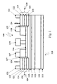
- FIG. 1 shows a schematic representation of an optically triggered power switch according to embodiments of the invention.
- the power switch 100 comprises an HEMT 110 and an APD 120.
- the HEMT 110 comprises a substrate 111 for example of silicon carbide material, a barrier or buffer layer 112 for example of GaN, a channel layer 113 for example of GaN which is preferably undoped, the buffer layer 112 and the channel layer 113 together having a thickness for example between 2000nm and 3000nm, a spacer layer 114 for example of AlGaN and preferably undoped having a thickness of for example 5nm, an AlGaN donor (or supply) layer 115 preferably being highly doped with n-type charge and having a wide band-gap with a thickness of for example 25nmn, a barrier layer 116 for example of AlGaN having a thickness of for example 3nm, a source terminal 117, a drain terminal 118 and a gate terminal 119.
- the layers described above may be constructed using known methods such as for example expitaxial growth techniques which are known to a person skilled in the art.
- the above described structure is to be considered as exemplary as regards layers as well as materials used. Those skilled in the related art will realize that other structures and materials may also be used in the construction of the HEMT.
- the APD 120 as shown in the figure is represented in two parts, each part at one side of the figure. However, it is to be noted that the two parts conform one APD as is described below.
- the APD may form a circular or rectangular ring around the gate electrode of the HEMT. However, these constructions are not mandatory and it may also be envisaged that the APD is placed at the center of the overall structure in case geometrical charge and field distribution within the device are of concern.
- the APD 120 may comprise an intrinsic photon absorption layer 124 for example of InAlN and a thickness of a few hundreds of nm, covered by a positive (p-type) doped multiplication region 125 for example of InN and a thickness of approximately 200nm, both sandwiched by a positive doped 125 and negative doped 122 InN-layer which in use are reversely biased.
- the APD also comprises contact electrodes 121.
- the layers described above may be constructed using known methods such as expitaxial growth techniques which are known to a person skilled in the art.
- the above described structure is to be considered as exemplary as regards layers as well as materials used. Those skilled in the related art will realize that other structures and materials may also be used in the construction of the APD.
- Isolation layer 127 isolates the APD structure 120 from parts of HEMT 110 where contact is to be avoided, for example with the source 117, drain 118 and the barrier layer 116.
- the APD is a current generating device, namely it generates an output current which is proportional to the optical input power.
- the HEMT however is an electrostatic device, hence it is controlled by electrical potential. Therefore in a practical implementation, there may arise a need for an impedance transforming element between the APD and the HEMT.
- This function in a conventional setup may be performed by a trans-impedance amplifier.
- the layers between the APD and the HEMT may be constructed such that one or more of them are capable of acting as a resistive element. This can be supported by a dedicated lateral doping profile in one or more of these layers.
- bias voltage is applied to electrodes 121, and light is injected in the APD as schematically shown in the figure by reference numeral 126. Therefore, the photons injected in the APD generate charge carriers which are accelerated in a high electrical field caused by the bias voltage applied to electrode 121 and which are subsequently multiplied according to avalanche effect.
- the accelerated and multiplied carriers travel from the APD into the carrier donor layer 115 of the HEMT 110 and as a consequence influence the electrical potential of the carrier donor layer 115 by modulating the density of free charge carriers, hence modulating the two dimensional electron gas (2DEG) which is built in a conduction layer between the donor layer 115 and the channel 113 of the HEMT.
- 2DEG two dimensional electron gas
- advantage is taken from the high electrical internal field which is usually present in the HEMT in order to enhance, as much as possible, the charge multiplication and/or acceleration in the avalanche diode.
- the power switch of the invention is in radio frequency applications, for example in Radio over Fiber applications, however other applications related to any optically controlled, and preferably fast, switch are also possible.
Landscapes
- Junction Field-Effect Transistors (AREA)
Abstract
Description
- The present invention relates to photonic devices. In particular, the invention relates to photonic devices which may be used for any optically controlled, and preferably fast, switch.
- Photonic devices for use as optically controlled, and preferably fast, switches may have a variety of applications.
- In order to ensure a reliable transmission, there is a need for sufficient power, and as consequence an efficient power amplifier. Some known solutions propose the use of new electronic circuit concepts such as envelope tracking amplifiers or switched (Class-S) amplifiers in order to increase power amplifier efficiency. However, most of the known solutions require the use of various devices such as optical/electrical converters, pre-amplifiers and the like. These solutions therefore involve a high device count resulting in additional cost, efficiency loss due to device matching circuits and wiring, as well as a decrease in system reliability.
- Embodiments of the present invention aim at providing an optically triggered power switch comprising an avalanche photo diode and a low loss switch element.
- According to some embodiments, there is provided a photonic power switch comprising an avalanche photo diode (APD) installed on a switch element, the switch element comprising a carrier donor layer and a channel layer, wherein the APD is disposed on the switch element such that accelerated charge carriers generated by photoeffect in an absorption region and output from the APD are input into a conduction layer generated between the carrier donor layer and the channel layer.
- According to some embodiments, there is provided a method of controlling current flow in a photonic power switch, the photonic power switch comprising an avalanche photo diode installed on a switch element, the switch element comprising a carrier donor layer and a channel layer, the method comprising the steps of injecting photons in the APD for generating electrical charge carriers by photoeffect, accelerating the generated charge carriers by an electric field so as to produce an avalanche effect, injecting the accelerated charge carriers from the APD into the carrier donor layer of the switch element and modulating a conduction layer built between the donor layer and the channel layer of the switch element, thereby modulating a current flow between a drain and a source of the power switch through said conduction layer.
- One particular use of the power switch of the invention is in radio frequency applications, for example in Radio over Fiber applications, however other applications related to any optically controlled, and preferably fast, switch are also possible.
- These and further features and advantages of the present invention are described in more detail in the following description as well as in the claims with the aid of the accompanying drawing.
-
-
Figure 1 is an exemplary schematic cross-section representation of an optically triggered power switch according to embodiments of the invention. - In the embodiments of the present invention a HEMT (High Electron Mobility Transistor) is used as a switch element, which in terms of basic structure is a known device. However, a brief description of a typical HEMT is herein provided in order to facilitate a better understanding of the embodiments of the invention.
- HEMT has a structure based on a field effect transistor where two materials with different band gaps are separated from each other by means of a layer usually called a junction. A first material may be for example AlGaN, or AlGaAs and a second material may be GaN or GaAs. Other materials may also be used depending on the type of application involved.
- The first material, for example AlGaN, may be typically a highly-doped n-type layer, typically with a wide band gap, the layer being typically called supply, or donor, layer. The second material, for example GaN, may be typically an undoped layer, typically with a narrow band gap, the layer being typically called channel layer. A junction is formed between the two layers containing high mobility electrons, the high mobility electrons being capable of allowing conduction through the junction, and thus through the device. The advantage of this type of devices is that they are capable of conducting levels of current which are significantly higher as compared to conventional FETs due to the absence of charge scattering by doping impurities and the relatively high electron mobility together with a superior carrier transport properties of the two dimensional electron gas created in the junction between the two layers. Therefore, they are useful in power applications. The conductivity of the carrier transport layer, and consequently the conductivity between source and drain terminals of the device is adjusted in the conventional devices by an adjustable voltage applied to the gate of the device.
- For the sake of clarity it is to be noted that the two dimensional electron gas (2DEG) is a known concept in the related art generally referring to a "gas" of electrons which are free to move in a two dimensions, the third dimension of the space used for the free movement being very narrow, and thus neglected for practical purposes.
- According to embodiments of the present invention, an avalanche photo diode structure (APD) is integrated with a HEMT structure. The APD is capable of causing acceleration of photon triggered carriers in a high electrical field thus giving rise to multiplication of the carriers by avalanche effect. The effect of an APD integrated with a HEMT structure may cause the accelerated carriers to influence the potential of the carrier supply layer, hence modulating the two dimensional electron gas (2DEG) of the HEMT inside a depletion layer. This manner of modulating the 2DEG is different from the known solutions where the gate electrode is used to control the response of a conventional HEMT.
- In addition, charge multiplication and/or acceleration in the APD may be drawn from the high electrical internal field usually being present during the operation of a GaN-based radio frequency power HEMT. Although this possibility is not mandatory, it is an additional advantage of the proposed structure because it helps to avoid a dedicated voltage supply for the APD by taking advantage of the already available high HEMT supply voltage.
-
Figure 1 shows a schematic representation of an optically triggered power switch according to embodiments of the invention. Thepower switch 100 comprises an HEMT 110 and anAPD 120. - The HEMT 110 comprises a
substrate 111 for example of silicon carbide material, a barrier orbuffer layer 112 for example of GaN, achannel layer 113 for example of GaN which is preferably undoped, thebuffer layer 112 and thechannel layer 113 together having a thickness for example between 2000nm and 3000nm, aspacer layer 114 for example of AlGaN and preferably undoped having a thickness of for example 5nm, an AlGaN donor (or supply)layer 115 preferably being highly doped with n-type charge and having a wide band-gap with a thickness of for example 25nmn, abarrier layer 116 for example of AlGaN having a thickness of for example 3nm, asource terminal 117, adrain terminal 118 and agate terminal 119. The layers described above may be constructed using known methods such as for example expitaxial growth techniques which are known to a person skilled in the art. The above described structure is to be considered as exemplary as regards layers as well as materials used. Those skilled in the related art will realize that other structures and materials may also be used in the construction of the HEMT. - The
APD 120 as shown in the figure is represented in two parts, each part at one side of the figure. However, it is to be noted that the two parts conform one APD as is described below. In practice, the APD may form a circular or rectangular ring around the gate electrode of the HEMT. However, these constructions are not mandatory and it may also be envisaged that the APD is placed at the center of the overall structure in case geometrical charge and field distribution within the device are of concern. - The
APD 120 may comprise an intrinsicphoton absorption layer 124 for example of InAlN and a thickness of a few hundreds of nm, covered by a positive (p-type) dopedmultiplication region 125 for example of InN and a thickness of approximately 200nm, both sandwiched by a positive doped 125 and negative doped 122 InN-layer which in use are reversely biased. The APD also comprisescontact electrodes 121. The layers described above may be constructed using known methods such as expitaxial growth techniques which are known to a person skilled in the art. The above described structure is to be considered as exemplary as regards layers as well as materials used. Those skilled in the related art will realize that other structures and materials may also be used in the construction of the APD. -
Isolation layer 127 isolates theAPD structure 120 from parts of HEMT 110 where contact is to be avoided, for example with thesource 117,drain 118 and thebarrier layer 116. - As it is known, the APD is a current generating device, namely it generates an output current which is proportional to the optical input power. The HEMT however is an electrostatic device, hence it is controlled by electrical potential. Therefore in a practical implementation, there may arise a need for an impedance transforming element between the APD and the HEMT. This function in a conventional setup may be performed by a trans-impedance amplifier. In the case of the present invention, the layers between the APD and the HEMT may be constructed such that one or more of them are capable of acting as a resistive element. This can be supported by a dedicated lateral doping profile in one or more of these layers.
- As it is known, by applying a relatively high reverse bias voltage, for example in the order of several tens of volts, an internal current gain effect is produced in the APD due to the so-called avalanche effect.
- In the embodiments of the present invention, bias voltage is applied to
electrodes 121, and light is injected in the APD as schematically shown in the figure byreference numeral 126. Therefore, the photons injected in the APD generate charge carriers which are accelerated in a high electrical field caused by the bias voltage applied toelectrode 121 and which are subsequently multiplied according to avalanche effect. The accelerated and multiplied carriers travel from the APD into thecarrier donor layer 115 of theHEMT 110 and as a consequence influence the electrical potential of thecarrier donor layer 115 by modulating the density of free charge carriers, hence modulating the two dimensional electron gas (2DEG) which is built in a conduction layer between thedonor layer 115 and thechannel 113 of the HEMT. In this manner, by optical excitation of the APD, the HEMT current throughput betweensource 117 and drain 118 terminals may be controlled and adjusted, thus controlling the power output of thedevice 100. - In fact, what is modulated in the present case is the electrical potential by modulation of charge carrier concentration. This approach distinguishes from the conventional approach of electrical control of the HEMT which is based on applying a voltage to the gate electrode. However, the still available gate electrode may be used for additional electrical modulation or for biasing.
- In addition, advantage is taken from the high electrical internal field which is usually present in the HEMT in order to enhance, as much as possible, the charge multiplication and/or acceleration in the avalanche diode.
- One particular use of the power switch of the invention is in radio frequency applications, for example in Radio over Fiber applications, however other applications related to any optically controlled, and preferably fast, switch are also possible.
- As regards advantages of the embodiments of the invention mention may be made to allowing for substantial reduction of device count (i.e. the number of elements used) for manufacturing photonic switched power amplifier concepts, such as for example in RF applications, thus improving efficiency and hardware usage for RF-power amplifiers in a BTS. Additionally the solution proposed herein helps to reduce susceptibility to failure due to integration of optical/electrical conversion, inherent signal mixing (by optical heterodyning) and final stage of switched RF-amplifier.
- Other advantages are improving power efficiency, improving overall system reliability, reducing susceptibility to noise interference.
Claims (7)
- An optically triggered photonic power switch comprising an avalanche photo diode and a switch element.
- The photonic power switch of claim 1, wherein the switch element comprises a carrier donor layer and a channel layer, wherein the avalanche photo diode is disposed on the switch element such that accelerated chare carriers generated by photoeffect in an absorption region and output from the avalanche photo diode are capable of being input into a conduction layer generated between the carrier donor layer and the channel layer.
- The photonic power switch of claim 1 or claim 2, wherein at least one layer between the avalanche photo diode and the switch element is a resistive element.
- A method of controlling current flow in a photonic power switch, the photonic power switch comprising an avalanche photo diode installed on a switch element, the switch element comprising a carrier donor layer and a channel layer, the method comprising the steps of injecting photons in the avalanche photo diode for generating electrical charge carriers by photoeffect, accelerating the generated charge carriers by an electric field so as to produce an avalanche effect, injecting the accelerated charge carriers from the avalanche photo diode into the carrier donor layer of the switch element and modulating a conduction layer built between the donor layer and the channel layer of the switch element, thereby modulating a current flow between a drain and a source of the power switch through said conduction layer.
- The method of claim 4 further comprising the step of providing an impendence by means of a resistive element present in at least one layer between the avalanche photo diode and the switch element.
- Use of the photonic power switch of any one of claims 1 to 3 in radio frequency applications.
- Use according to claim 6 wherein such use is in radio over fiber.
Priority Applications (2)
| Application Number | Priority Date | Filing Date | Title |
|---|---|---|---|
| EP08305566.5A EP2166579B1 (en) | 2008-09-18 | 2008-09-18 | Photonic power switch and method of controlling current flow in the photonic power switch and use of such photonic power switch |
| US12/461,841 US8373242B2 (en) | 2008-09-18 | 2009-08-26 | Photonic power switch and method of controlling current flow in the photonic power switch and use of such photonic power switch |
Applications Claiming Priority (1)
| Application Number | Priority Date | Filing Date | Title |
|---|---|---|---|
| EP08305566.5A EP2166579B1 (en) | 2008-09-18 | 2008-09-18 | Photonic power switch and method of controlling current flow in the photonic power switch and use of such photonic power switch |
Publications (2)
| Publication Number | Publication Date |
|---|---|
| EP2166579A1 true EP2166579A1 (en) | 2010-03-24 |
| EP2166579B1 EP2166579B1 (en) | 2016-05-04 |
Family
ID=40380385
Family Applications (1)
| Application Number | Title | Priority Date | Filing Date |
|---|---|---|---|
| EP08305566.5A Not-in-force EP2166579B1 (en) | 2008-09-18 | 2008-09-18 | Photonic power switch and method of controlling current flow in the photonic power switch and use of such photonic power switch |
Country Status (2)
| Country | Link |
|---|---|
| US (1) | US8373242B2 (en) |
| EP (1) | EP2166579B1 (en) |
Families Citing this family (2)
| Publication number | Priority date | Publication date | Assignee | Title |
|---|---|---|---|---|
| EP2166579B1 (en) * | 2008-09-18 | 2016-05-04 | Alcatel Lucent | Photonic power switch and method of controlling current flow in the photonic power switch and use of such photonic power switch |
| US11340512B2 (en) * | 2020-04-27 | 2022-05-24 | Raytheon Bbn Technologies Corp. | Integration of electronics with Lithium Niobate photonics |
Citations (4)
| Publication number | Priority date | Publication date | Assignee | Title |
|---|---|---|---|---|
| EP0757392A1 (en) * | 1995-08-03 | 1997-02-05 | Hitachi Europe Limited | Semiconductor structures |
| US20030047752A1 (en) * | 2000-09-29 | 2003-03-13 | Campbell Joe C. | Avalanche photodiodes with an impact-ionization-engineered multiplication region |
| US20040251483A1 (en) * | 2002-02-01 | 2004-12-16 | Ko Cheng C. | Planar avalanche photodiode |
| US20070221827A1 (en) * | 2006-03-21 | 2007-09-27 | Fathimulla Ayub M | Photon counting optically preamplified photoreceivers with micro-digitized pixels |
Family Cites Families (4)
| Publication number | Priority date | Publication date | Assignee | Title |
|---|---|---|---|---|
| EP0233725B1 (en) * | 1986-02-18 | 1995-04-19 | Kabushiki Kaisha Toshiba | Opto-Electronic Device and Method for its Manufacture |
| US6987306B2 (en) * | 2003-07-17 | 2006-01-17 | Epitaxial Technologies | Monolithic photoreceiver technology for free space optical networks |
| US6969896B1 (en) * | 2003-08-12 | 2005-11-29 | Varian Medical Systems Technologies, Inc. | Photodetector biasing scheme |
| EP2166579B1 (en) * | 2008-09-18 | 2016-05-04 | Alcatel Lucent | Photonic power switch and method of controlling current flow in the photonic power switch and use of such photonic power switch |
-
2008
- 2008-09-18 EP EP08305566.5A patent/EP2166579B1/en not_active Not-in-force
-
2009
- 2009-08-26 US US12/461,841 patent/US8373242B2/en not_active Expired - Fee Related
Patent Citations (4)
| Publication number | Priority date | Publication date | Assignee | Title |
|---|---|---|---|---|
| EP0757392A1 (en) * | 1995-08-03 | 1997-02-05 | Hitachi Europe Limited | Semiconductor structures |
| US20030047752A1 (en) * | 2000-09-29 | 2003-03-13 | Campbell Joe C. | Avalanche photodiodes with an impact-ionization-engineered multiplication region |
| US20040251483A1 (en) * | 2002-02-01 | 2004-12-16 | Ko Cheng C. | Planar avalanche photodiode |
| US20070221827A1 (en) * | 2006-03-21 | 2007-09-27 | Fathimulla Ayub M | Photon counting optically preamplified photoreceivers with micro-digitized pixels |
Also Published As
| Publication number | Publication date |
|---|---|
| US8373242B2 (en) | 2013-02-12 |
| EP2166579B1 (en) | 2016-05-04 |
| US20100065937A1 (en) | 2010-03-18 |
Similar Documents
| Publication | Publication Date | Title |
|---|---|---|
| JP6921368B2 (en) | Isolated III-N semiconductor device | |
| JP3129298B2 (en) | Field effect transistor and method of manufacturing the same | |
| US11424382B2 (en) | Electrical devices making use of counterdoped junctions | |
| JP2011124572A (en) | High voltage durability iii-nitride semiconductor device | |
| WO2014184995A1 (en) | Nitride semiconductor device | |
| JP5179694B2 (en) | Heterostructure doped with donor on the back side | |
| US6835969B1 (en) | Split-channel high electron mobility transistor (HEMT) device | |
| US8373242B2 (en) | Photonic power switch and method of controlling current flow in the photonic power switch and use of such photonic power switch | |
| JP4371668B2 (en) | Semiconductor device | |
| JP2000349096A (en) | Compound field effect transistor and method of manufacturing the same | |
| CN112466954B (en) | Semiconductor device and manufacturing method thereof | |
| JP4913324B2 (en) | Field effect transistor | |
| US8193566B2 (en) | Semiconductor device | |
| US9793430B1 (en) | Heterojunction schottky gate bipolar transistor | |
| Ghione et al. | Guest editorial special issue on GaN electronic devices | |
| JP7794309B2 (en) | field-effect transistor | |
| KR100553963B1 (en) | Field effect transistor | |
| CN119069522B (en) | transistors and electronic devices | |
| JP2003289082A (en) | Semiconductor device for communication equipment and equipment for communication system | |
| CN101501827A (en) | Device and method of manufacture for a low noise junction field effect transistor | |
| Xiong | Gallium Nitride Integrated Circuits for High-Voltage and High-Temperature Applications | |
| JPH10116837A (en) | Field effect type semiconductor device | |
| US11283021B2 (en) | Compound semiconductor device including MOTT insulator for preventing device damage due to high-energy particles | |
| WO2025188695A1 (en) | High power diamond transistors with electrical and optical gate control | |
| JP2011146512A (en) | Semiconductor apparatus |
Legal Events
| Date | Code | Title | Description |
|---|---|---|---|
| PUAI | Public reference made under article 153(3) epc to a published international application that has entered the european phase |
Free format text: ORIGINAL CODE: 0009012 |
|
| AK | Designated contracting states |
Kind code of ref document: A1 Designated state(s): AT BE BG CH CY CZ DE DK EE ES FI FR GB GR HR HU IE IS IT LI LT LU LV MC MT NL NO PL PT RO SE SI SK TR |
|
| AX | Request for extension of the european patent |
Extension state: AL BA MK RS |
|
| 17P | Request for examination filed |
Effective date: 20100924 |
|
| 17Q | First examination report despatched |
Effective date: 20101015 |
|
| AKX | Designation fees paid |
Designated state(s): AT BE BG CH CY CZ DE DK EE ES FI FR GB GR HR HU IE IS IT LI LT LU LV MC MT NL NO PL PT RO SE SI SK TR |
|
| RAP1 | Party data changed (applicant data changed or rights of an application transferred) |
Owner name: ALCATEL LUCENT |
|
| 111Z | Information provided on other rights and legal means of execution |
Free format text: AT BE BG CH CY CZ DE DK EE ES FI FR GB GR HR HU IE IS IT LI LT LU LV MC MT NL NO PL PT RO SE SI SK TR Effective date: 20130410 |
|
| RAP1 | Party data changed (applicant data changed or rights of an application transferred) |
Owner name: ALCATEL LUCENT |
|
| D11X | Information provided on other rights and legal means of execution (deleted) | ||
| GRAP | Despatch of communication of intention to grant a patent |
Free format text: ORIGINAL CODE: EPIDOSNIGR1 |
|
| INTG | Intention to grant announced |
Effective date: 20151125 |
|
| GRAS | Grant fee paid |
Free format text: ORIGINAL CODE: EPIDOSNIGR3 |
|
| GRAA | (expected) grant |
Free format text: ORIGINAL CODE: 0009210 |
|
| AK | Designated contracting states |
Kind code of ref document: B1 Designated state(s): AT BE BG CH CY CZ DE DK EE ES FI FR GB GR HR HU IE IS IT LI LT LU LV MC MT NL NO PL PT RO SE SI SK TR |
|
| REG | Reference to a national code |
Ref country code: GB Ref legal event code: FG4D |
|
| REG | Reference to a national code |
Ref country code: CH Ref legal event code: EP |
|
| REG | Reference to a national code |
Ref country code: AT Ref legal event code: REF Ref document number: 797591 Country of ref document: AT Kind code of ref document: T Effective date: 20160515 |
|
| REG | Reference to a national code |
Ref country code: IE Ref legal event code: FG4D |
|
| REG | Reference to a national code |
Ref country code: DE Ref legal event code: R096 Ref document number: 602008043971 Country of ref document: DE |
|
| REG | Reference to a national code |
Ref country code: NL Ref legal event code: MP Effective date: 20160504 |
|
| REG | Reference to a national code |
Ref country code: LT Ref legal event code: MG4D |
|
| REG | Reference to a national code |
Ref country code: FR Ref legal event code: PLFP Year of fee payment: 9 |
|
| PG25 | Lapsed in a contracting state [announced via postgrant information from national office to epo] |
Ref country code: NL Free format text: LAPSE BECAUSE OF FAILURE TO SUBMIT A TRANSLATION OF THE DESCRIPTION OR TO PAY THE FEE WITHIN THE PRESCRIBED TIME-LIMIT Effective date: 20160504 Ref country code: FI Free format text: LAPSE BECAUSE OF FAILURE TO SUBMIT A TRANSLATION OF THE DESCRIPTION OR TO PAY THE FEE WITHIN THE PRESCRIBED TIME-LIMIT Effective date: 20160504 Ref country code: NO Free format text: LAPSE BECAUSE OF FAILURE TO SUBMIT A TRANSLATION OF THE DESCRIPTION OR TO PAY THE FEE WITHIN THE PRESCRIBED TIME-LIMIT Effective date: 20160804 Ref country code: LT Free format text: LAPSE BECAUSE OF FAILURE TO SUBMIT A TRANSLATION OF THE DESCRIPTION OR TO PAY THE FEE WITHIN THE PRESCRIBED TIME-LIMIT Effective date: 20160504 |
|
| REG | Reference to a national code |
Ref country code: AT Ref legal event code: MK05 Ref document number: 797591 Country of ref document: AT Kind code of ref document: T Effective date: 20160504 |
|
| PG25 | Lapsed in a contracting state [announced via postgrant information from national office to epo] |
Ref country code: GR Free format text: LAPSE BECAUSE OF FAILURE TO SUBMIT A TRANSLATION OF THE DESCRIPTION OR TO PAY THE FEE WITHIN THE PRESCRIBED TIME-LIMIT Effective date: 20160805 Ref country code: LV Free format text: LAPSE BECAUSE OF FAILURE TO SUBMIT A TRANSLATION OF THE DESCRIPTION OR TO PAY THE FEE WITHIN THE PRESCRIBED TIME-LIMIT Effective date: 20160504 Ref country code: SE Free format text: LAPSE BECAUSE OF FAILURE TO SUBMIT A TRANSLATION OF THE DESCRIPTION OR TO PAY THE FEE WITHIN THE PRESCRIBED TIME-LIMIT Effective date: 20160504 Ref country code: HR Free format text: LAPSE BECAUSE OF FAILURE TO SUBMIT A TRANSLATION OF THE DESCRIPTION OR TO PAY THE FEE WITHIN THE PRESCRIBED TIME-LIMIT Effective date: 20160504 Ref country code: ES Free format text: LAPSE BECAUSE OF FAILURE TO SUBMIT A TRANSLATION OF THE DESCRIPTION OR TO PAY THE FEE WITHIN THE PRESCRIBED TIME-LIMIT Effective date: 20160504 Ref country code: PT Free format text: LAPSE BECAUSE OF FAILURE TO SUBMIT A TRANSLATION OF THE DESCRIPTION OR TO PAY THE FEE WITHIN THE PRESCRIBED TIME-LIMIT Effective date: 20160905 |
|
| PG25 | Lapsed in a contracting state [announced via postgrant information from national office to epo] |
Ref country code: IT Free format text: LAPSE BECAUSE OF FAILURE TO SUBMIT A TRANSLATION OF THE DESCRIPTION OR TO PAY THE FEE WITHIN THE PRESCRIBED TIME-LIMIT Effective date: 20160504 |
|
| PG25 | Lapsed in a contracting state [announced via postgrant information from national office to epo] |
Ref country code: RO Free format text: LAPSE BECAUSE OF FAILURE TO SUBMIT A TRANSLATION OF THE DESCRIPTION OR TO PAY THE FEE WITHIN THE PRESCRIBED TIME-LIMIT Effective date: 20160504 Ref country code: SK Free format text: LAPSE BECAUSE OF FAILURE TO SUBMIT A TRANSLATION OF THE DESCRIPTION OR TO PAY THE FEE WITHIN THE PRESCRIBED TIME-LIMIT Effective date: 20160504 Ref country code: CZ Free format text: LAPSE BECAUSE OF FAILURE TO SUBMIT A TRANSLATION OF THE DESCRIPTION OR TO PAY THE FEE WITHIN THE PRESCRIBED TIME-LIMIT Effective date: 20160504 Ref country code: DK Free format text: LAPSE BECAUSE OF FAILURE TO SUBMIT A TRANSLATION OF THE DESCRIPTION OR TO PAY THE FEE WITHIN THE PRESCRIBED TIME-LIMIT Effective date: 20160504 Ref country code: EE Free format text: LAPSE BECAUSE OF FAILURE TO SUBMIT A TRANSLATION OF THE DESCRIPTION OR TO PAY THE FEE WITHIN THE PRESCRIBED TIME-LIMIT Effective date: 20160504 |
|
| REG | Reference to a national code |
Ref country code: DE Ref legal event code: R097 Ref document number: 602008043971 Country of ref document: DE |
|
| PG25 | Lapsed in a contracting state [announced via postgrant information from national office to epo] |
Ref country code: BE Free format text: LAPSE BECAUSE OF NON-PAYMENT OF DUE FEES Effective date: 20160504 Ref country code: AT Free format text: LAPSE BECAUSE OF FAILURE TO SUBMIT A TRANSLATION OF THE DESCRIPTION OR TO PAY THE FEE WITHIN THE PRESCRIBED TIME-LIMIT Effective date: 20160504 Ref country code: PL Free format text: LAPSE BECAUSE OF FAILURE TO SUBMIT A TRANSLATION OF THE DESCRIPTION OR TO PAY THE FEE WITHIN THE PRESCRIBED TIME-LIMIT Effective date: 20160504 |
|
| PLBE | No opposition filed within time limit |
Free format text: ORIGINAL CODE: 0009261 |
|
| STAA | Information on the status of an ep patent application or granted ep patent |
Free format text: STATUS: NO OPPOSITION FILED WITHIN TIME LIMIT |
|
| 26N | No opposition filed |
Effective date: 20170207 |
|
| PG25 | Lapsed in a contracting state [announced via postgrant information from national office to epo] |
Ref country code: MC Free format text: LAPSE BECAUSE OF FAILURE TO SUBMIT A TRANSLATION OF THE DESCRIPTION OR TO PAY THE FEE WITHIN THE PRESCRIBED TIME-LIMIT Effective date: 20160504 |
|
| REG | Reference to a national code |
Ref country code: CH Ref legal event code: PL |
|
| PG25 | Lapsed in a contracting state [announced via postgrant information from national office to epo] |
Ref country code: SI Free format text: LAPSE BECAUSE OF FAILURE TO SUBMIT A TRANSLATION OF THE DESCRIPTION OR TO PAY THE FEE WITHIN THE PRESCRIBED TIME-LIMIT Effective date: 20160504 |
|
| REG | Reference to a national code |
Ref country code: IE Ref legal event code: MM4A |
|
| PG25 | Lapsed in a contracting state [announced via postgrant information from national office to epo] |
Ref country code: CH Free format text: LAPSE BECAUSE OF NON-PAYMENT OF DUE FEES Effective date: 20160930 Ref country code: LI Free format text: LAPSE BECAUSE OF NON-PAYMENT OF DUE FEES Effective date: 20160930 Ref country code: IE Free format text: LAPSE BECAUSE OF NON-PAYMENT OF DUE FEES Effective date: 20160918 |
|
| PG25 | Lapsed in a contracting state [announced via postgrant information from national office to epo] |
Ref country code: LU Free format text: LAPSE BECAUSE OF NON-PAYMENT OF DUE FEES Effective date: 20160918 |
|
| REG | Reference to a national code |
Ref country code: FR Ref legal event code: PLFP Year of fee payment: 10 |
|
| PGFP | Annual fee paid to national office [announced via postgrant information from national office to epo] |
Ref country code: GB Payment date: 20170921 Year of fee payment: 10 Ref country code: FR Payment date: 20170928 Year of fee payment: 10 Ref country code: DE Payment date: 20170928 Year of fee payment: 10 |
|
| PG25 | Lapsed in a contracting state [announced via postgrant information from national office to epo] |
Ref country code: HU Free format text: LAPSE BECAUSE OF FAILURE TO SUBMIT A TRANSLATION OF THE DESCRIPTION OR TO PAY THE FEE WITHIN THE PRESCRIBED TIME-LIMIT; INVALID AB INITIO Effective date: 20080918 Ref country code: CY Free format text: LAPSE BECAUSE OF FAILURE TO SUBMIT A TRANSLATION OF THE DESCRIPTION OR TO PAY THE FEE WITHIN THE PRESCRIBED TIME-LIMIT Effective date: 20160504 |
|
| PG25 | Lapsed in a contracting state [announced via postgrant information from national office to epo] |
Ref country code: IS Free format text: LAPSE BECAUSE OF FAILURE TO SUBMIT A TRANSLATION OF THE DESCRIPTION OR TO PAY THE FEE WITHIN THE PRESCRIBED TIME-LIMIT Effective date: 20160504 Ref country code: TR Free format text: LAPSE BECAUSE OF FAILURE TO SUBMIT A TRANSLATION OF THE DESCRIPTION OR TO PAY THE FEE WITHIN THE PRESCRIBED TIME-LIMIT Effective date: 20160504 Ref country code: MT Free format text: LAPSE BECAUSE OF NON-PAYMENT OF DUE FEES Effective date: 20160930 |
|
| PG25 | Lapsed in a contracting state [announced via postgrant information from national office to epo] |
Ref country code: BG Free format text: LAPSE BECAUSE OF FAILURE TO SUBMIT A TRANSLATION OF THE DESCRIPTION OR TO PAY THE FEE WITHIN THE PRESCRIBED TIME-LIMIT Effective date: 20160504 |
|
| REG | Reference to a national code |
Ref country code: DE Ref legal event code: R119 Ref document number: 602008043971 Country of ref document: DE |
|
| REG | Reference to a national code |
Ref country code: DE Ref legal event code: R082 Ref document number: 602008043971 Country of ref document: DE Representative=s name: MENZIETTI WETZEL, DE Ref country code: DE Ref legal event code: R081 Ref document number: 602008043971 Country of ref document: DE Owner name: PROVENANCE ASSET GROUP LLC, PITTSFORD, US Free format text: FORMER OWNER: ALCATEL LUCENT, BOULOGNE BILLANCOURT, FR |
|
| REG | Reference to a national code |
Ref country code: GB Ref legal event code: 732E Free format text: REGISTERED BETWEEN 20190418 AND 20190426 |
|
| GBPC | Gb: european patent ceased through non-payment of renewal fee |
Effective date: 20180918 |
|
| PG25 | Lapsed in a contracting state [announced via postgrant information from national office to epo] |
Ref country code: DE Free format text: LAPSE BECAUSE OF NON-PAYMENT OF DUE FEES Effective date: 20190402 |
|
| PG25 | Lapsed in a contracting state [announced via postgrant information from national office to epo] |
Ref country code: FR Free format text: LAPSE BECAUSE OF NON-PAYMENT OF DUE FEES Effective date: 20180930 |
|
| PG25 | Lapsed in a contracting state [announced via postgrant information from national office to epo] |
Ref country code: GB Free format text: LAPSE BECAUSE OF NON-PAYMENT OF DUE FEES Effective date: 20180918 |