EP2164192B1 - Low noise block control - Google Patents
Low noise block control Download PDFInfo
- Publication number
- EP2164192B1 EP2164192B1 EP09169553.6A EP09169553A EP2164192B1 EP 2164192 B1 EP2164192 B1 EP 2164192B1 EP 09169553 A EP09169553 A EP 09169553A EP 2164192 B1 EP2164192 B1 EP 2164192B1
- Authority
- EP
- European Patent Office
- Prior art keywords
- signal
- control
- control circuit
- power
- power supply
- Prior art date
- Legal status (The legal status is an assumption and is not a legal conclusion. Google has not performed a legal analysis and makes no representation as to the accuracy of the status listed.)
- Active
Links
Images


Classifications
-
- H—ELECTRICITY
- H04—ELECTRIC COMMUNICATION TECHNIQUE
- H04H—BROADCAST COMMUNICATION
- H04H40/00—Arrangements specially adapted for receiving broadcast information
- H04H40/18—Arrangements characterised by circuits or components specially adapted for receiving
- H04H40/27—Arrangements characterised by circuits or components specially adapted for receiving specially adapted for broadcast systems covered by groups H04H20/53 - H04H20/95
- H04H40/90—Arrangements characterised by circuits or components specially adapted for receiving specially adapted for broadcast systems covered by groups H04H20/53 - H04H20/95 specially adapted for satellite broadcast receiving
Definitions
- the present invention relates to an apparatus for controlling a low noise block and to a method for communicating with a low noise block.
- Satellite television systems are commonplace in today's households. Generally, such systems provide a television signal to a user from an orbiting satellite. The television signal may then be collected by a parabolic satellite dish or dishes located near the user. Once collected, the signal is transmitted to a set-top box (STB) which translates and provides the received signal to a user's television such that the user's television recognizes and displays a television program to the user.
- STB set-top box
- the satellite dish may include a low noise block (LNB) device.
- the LNB acts as the antenna of the satellite dish by collecting the transmitted television signal and providing that signal to an STB. Further, because satellites generally use a high frequency signal when transmitting the television signal, the LNB also converts the signal into a lower frequency and amplifies the signal before transmitting the signal to the STB. By converting the signal into a lower frequency, the signal may be transmitted across a cable able to connect the STB and the LNB with less loss.
- LNB low noise block
- the cable connecting the STB and the LNB can also carry power and communication signals. These signals are transmitted from the STB to the LNB through the cable.
- the power and communication signals sent from the STB to the LNB can be used to control one or several LNBs.
- the STB provides signals to the LNBs to switch from one LNB to another in response to an input provided by the user.
- the STB may provide signals to switch from a first LNB and to a second LNB to access the requested channel. In this manner, the STB may supply power to the LNB as well as provide communication signals to the LNB to control the LNB device.
- the present invention seeks to provide an apparatus and a method for controlling a low noise block.
- WO2007040573 (A1 ) describes a method for selecting antenna configurations in a satellite receiving system. The method proceeds by selecting antenna configurations using a first mode of operation wherein frequency shift keying ("FSK") of a frequency is implemented, or a second mode of operation wherein a DC level is implemented, and adaptively controlling a capacitor to condition a signal while the second mode is in use and removing the effects of the capacitor while the first mode is in use.
- FSK frequency shift keying
- US2005130582 (A1 ) describes a low-noise block (LNB) control device within a set-top box.
- the LNB control device is capable of controlling modulation of an alternating waveform on a direct current (DC) voltage from a DC power supply to an LNB amplifier.
- the LNB control device includes a power supply control module, an LNB signaling module and a switch.
- the power supply control module sends a control signal to the DC power supply.
- the LNB signaling module provides a switch control signal and a modulating waveform to the switch. Under the control of switch control signal, the switch selectively sends the modulating waveform to a summing circuit that is located external to the LNB control device. Within the summing circuit, the modulating waveform is added to the DC voltage from the DC power supply.
- an apparatus for controlling a low noise block comprising:
- the apparatus comprises a power supply coupled to the power signal input of the control circuit, wherein the power supply inputs a power signal on the power signal input.
- the power supply may be a switch mode converter power supply.
- the apparatus comprises microprocessor coupled to the control signal input of the control circuit, wherein the microprocessor inputs a control signal on the control signal input. In an embodiment, the microprocessor inputs an enable signal on the enable signal input.
- a high enable signal causes a low impedance level at the output, the low impedance level facilitating transmission of a combined power and control signal at the output.
- a low enable signal causes a high impedance level at the output, the high impedance level facilitating the receipt of a communication signal from the low noise block to the control circuit.
- the FET comprises a base terminal, a source terminal, a gate terminal and a drain terminal, wherein the source terminal is electrically connected to the first resistor and the base terminal and the drain terminal are electrically connected to ground.
- the enable signal input is electrically connected to the gate terminal of the field effect transistor, wherein an enable signal is inputted on the enable signal input to control flow of current through the field effect transistor and thereby control the impedance level at the first node.
- the microprocessor and the power supply may be components of a set-top box.
- control signal and the power signal are combined and outputted at the first node.
- a second resistor is provided and is electrically connected to the second node to receive the control signal.
- the present invention also extends to a method for communicating with a low noise block comprising:
- the method comprises inputting a TTL enable signal to the body of the field-effect transistor device; and receiving a communication signal from the low noise block.
- the method comprises attenuating high frequency signals past a cutoff frequency in the power signal.
- control signal and the enable signal are generated by a microprocessor.
- the combined power and control signal provides power to the low noise block and control the functions of the low noise block.
- the control circuit provides a combined power signal and control signal to an LNB of a satellite system.
- the control circuit output may be transmitted to an LNB by a set-top box (STB) such that the STB may control the LNB.
- STB set-top box
- the control circuit may accept an enable signal from the STB to alter the circuit from a transmitting circuit to a receiving circuit.
- the control circuit may also integrate the functionality of a low pass filter into the communication signal circuit, thereby removing the need for a low pass filter at a power supply output.
- the control circuit may also lower the overall power consumption for the circuit by isolating the communication signal from the power supply signal before the signals are combined.
- the STB may power and control the LNB of the satellite system.
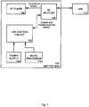
- Figure 1 depicts a block diagram of an arrangement of some components of an STB and an LNB of a satellite television system.
- the television system may receive a transmitted television signal and translate the signal such that a user's television may recognize and display a television program to the user.
- the television signal may be collected by the LNB 110 and transmitted to the STB 120.
- the collected signal may be transmitted to the STB 120 over a cable, such as a coaxial cable.
- the LNB may convert the signal into a lower frequency and amplify the signal before transmitting the signal to the STB 120.
- the transmitted signal may be received at the STB 120 by an RF splitter 130.
- the RF splitter 130 may split the incoming signal, sending the RF television signal to an RF tuner 140 and an LF communication signal to the LNB control circuit 150.
- the RF tuner 140 may utilize the incoming television signal to provide the user's television with a recognizable television signal.
- the LNB control circuit 150 may utilize the incoming communication signal to communicate and control the LNB 110.
- the LNB control circuit 150 may provide a power and communication signal to control the LNB 110.
- the LNB control circuit 150 may accept the power signal from a power supply 160 and the communication signal from a micro processor 170. Alternatively, the power supply 160 and the micro processor 170 may be a part of the LNB control circuit 150. Regardless, the LNB control circuit 150 may provide a combined power and communication signal to the LNB 110 through the RF splitter 130 of the STB 120. The combined power and communication signal may provide power to the LNB 110 as well as a communication signal to control the LNB. Thus, the LNB 110 may be controlled by the STB 120 by utilizing the LNB control circuit 150.
- Figure 2 depicts a prior art LNB control circuit 200, including a power supply circuit 210, a low pass filter circuit 220 and a communication circuit 230.
- the control circuit 200 of Figure 2 may be located within an STB and may provide a power signal to the LNB. Further, the communication circuit 230 may combine a control signal with the power signal to transmit to the LNB, such that the STB may both power and control the LNB.
- the power supply circuit 210 may include a power supply 212.
- the power supply 212 may be used by the control circuit 200 to provide power to the LNB through a cable connecting the STB to the LNB.
- the power supply 212 may be a switch mode converter that generates 13 or 18 volts DC.
- some drawbacks may exist with a switch mode converter power supply.
- the converter may cause switching noise at the power supply output that may be undesirable in certain circuits.
- a low pass filter is commonly used at the power supply output to filter out the switching noise.
- the low pass filter circuit 220 may include an inductor 222 and a capacitor 224 electrically connected in series.
- the inductor 222 and capacitor 224 may act on the output of the switch mode converter power supply as a low pass filter to filter out the noise caused by the switching of the switch mode converter power supply.
- the communication circuit 130 may receive a control instruction from the STB and combine it with the power signal generated by the power circuit 210 for transmission to the LNB.
- the control instruction may be generated by the STB and may be input to the circuit at the carrier insert input pin.
- the first resistor 232, the inductor 234 and the capacitor 236 of the communication circuit may form an RLC damped resonant circuit to remove harmonics from the control instruction signal on the carrier insert pin.
- the transistor 238, the second resistor 240 and the third resistor 242 may shift the voltage level of the incoming control instruction signal to the voltage of the power circuit 210.
- the control circuit 200 may provide a combined power signal and communication signal to the LNB.
- a field-effect transistor (FET) device 244 may be included in the control circuit 200 and electrically connected in series with the first resistor 232.
- the FET device 244 may operate as a switch in the control circuit 200 and may be controlled by an enable input.
- the FET device 244 may allow the circuit to change electrical impedance at the output. For example, a low impedance at the output pin may be achieved when the FET device 244 is conducting. The high impedance at the output pin may be achieved when the FET device 244 is not conducting.
- the enable signal that controls the FET device 244 may be provided by a microprocessor within the STB.
- a low voltage digital signal to control the FET device 244 may be adapted via an interface circuit 245 to raise the input voltage of the FET device to match that of the power supply 212.
- the control circuit 200 may use an additional interface circuit 245 at the enable pin input to increase the voltage of the enable signal.
- Figure 3 depicts one embodiment for a control circuit to provide power and control signals to an LNB device.
- the control circuit 300 may be located within a STB and may communicate with the LNB over a cable that connects the STB and the LNB.
- the control circuit 300 may be a separate module from the STB located between the STB and the LNB.
- such a configuration may utilize several connections between the control circuit 300 and the STB to provide the control circuit with the control and power signals.
- the power signal and communication signal may be combined by the control circuit 300 and may be transmitted to the LNB over this cable.
- a power supply 302 may be connected to the control circuit to provide power to the LNB.
- the power supply 302 depicted in Figure 3 merely represents a power supply signal connected to the control circuit.
- the power signal may come from any power source.
- the power supply may be a switched mode power supply connected directly to the control circuit 300.
- the power supply 302 may be supplied by a power circuit that modifies the power signal to meet the specifications of the control circuit.
- the power supply 302 may be any power signal that may be used by the STB to power the LNB.
- a typical power supply signal to power an LNB may range from 13 to 18 volts DC.
- One terminal of an inductor 304 may be electrically connected to the power supply 302 and the other terminal of the inductor 304 may be electrically connected to a first node 316.
- a first capacitor 306 may also be operably connected to the first node 316.
- the first capacitor 306 may also be connected on the other end to ground.
- the inductor 304 may be any electrical device that can store energy and resist current shifts.
- the first capacitor 306 may be any electrical device that can store electrical energy.
- the inductor 304 and the first capacitor 306 may act as a low pass filter for the incoming power supply signal.
- a low pass filter is an electronic circuit that passes low-frequency signals but attenuates highfrequency signals past a cutoff frequency. The cutoff frequency may be set by the values selected for the components that make up the low pass filter.
- the low pass filter function may filter out high frequency noise caused by the switching of the power supply 302, called switching ripple. In some circuits, switching ripple may be undesirable within the power signal. Thus, a low pass filter may be used to filter out the switching ripple. While shown as comprising the inductor 304 and the first capacitor 306, any low pass filter device that may remove high frequency signals but pass low frequency signals from the power supply signal may be used as the low pass filter.
- the use of a low pass filter that does not include an inductor 304 and a capacitor 306 may add additional components and cost to the control circuit 300.
- the inductor 304 and the first capacitor 306 may also be part of a damped resonant circuit to remove harmonics in the control circuit 300.
- the second capacitor 308 may be any electrical device that can store electrical energy, similar to the first capacitor 306 described above. As explained in more detail below, the second capacitor 308 may function to isolate the second resistor 312 and the carrier insert signal from the power supply signal.
- a second resistor 312 may also be connected to the second node 318.
- the second resistor 312, the inductor 304 and the first capacitor 306 may form an RLC damped resonant circuit.
- the damped resonant circuit may remove harmonics in the circuit that are created by a control signal inputted into the circuit at the carrier insert pin.
- a third resistor 310 may be electrically connected in series between the second node 318 and the carrier insert pin.
- the control signal input at the carrier insert pin may be generated by the STB to control the LNB.
- the STB may provide a control signal to the LNB to instruct the LNB to begin processing the incoming television signal.
- the control signal transmitted by the STB may be generated by a digital circuit at a transistor-transistor logic (TTL) voltage level.
- TTL transistor-transistor logic
- the control signal input on the carrier insert pin may be generated by a microprocessor or digital circuit of the STB.
- This control signal may be generated in the same manner as described with reference to Figure 2 .
- this embodiment may not provide for matching the control signal voltage to the power supply voltage level. Instead, because the carrier insert pin is isolated from the power supply signal, the control signal may be inputted at a TTL voltage level.
- the control signal may be provided by a microprocessor within the STB without additional components to increase the voltage level of the control signal.
- An output pin may be electrically connected to the first node of the control circuit 300.
- the control circuit 300 may provide a combined power signal and communication signal to the LNB.
- the combined signals may be in a form such that the signal is capable of being transmitted to the LNB over a cable that connects the STB and the LNB. Further, the output pin may be combined with the RF signal being input into the STB tuner from the LNB.
- the control circuit 300 for the LNB may be bi-directional.
- the control circuit 300 may provide a low impedance at the output pin when data is being sent from the circuit and may have high impedance when the LNB is providing the incoming communication signal to the control circuit 300.
- a field-effect transistor (FET) device 314 may be electrically connected in series between the second resistor 312 and ground.
- the FET device 314 of Figure 3 is an n-channel metal oxide semiconductor field-effect transistor, or n-channel "MOSFET.” It should be noted that alternative embodiments may use a p-channel MOSFET, depletion mode MOSFET, and so on.
- the FET device 314 may have four terminals, namely a gate, a drain, a source and a body.
- the gate terminal may be electrically connected to the second resistor 312.
- the drain and the source terminals may be connected to ground.
- the body terminal may be connected to an enable input signal.
- the FET device 314 receives an enable signal, the FET may act as a switch connecting the second resistor 312 to ground.
- the enable signal is removed from the FET device 314, the circuit becomes open at the FET device.
- the enable signal may control the bi-directional nature of the control circuit 300.
- a low impedance at the output pin may be useful.
- Low impedance at the output pin may be achieved by activating the FET device 312 and connecting the second resistor 312 to ground.
- a high input impedance may be required at the output pin.
- a high impedance at the output pin may be achieved when the FET device 312 is not conducting, thereby opening the circuit at the FET device.
- the control of the FET device 314 may be provided by a microprocessor or similar digital circuit signal within the STB.
- the STB may control when the control circuit 300 transmits data and when the circuit is blocked from receiving the incoming television signal.
- the enable signal provided to the FET device 314 may not require any additional circuitry to match the power supply 302 voltage.
- the second resistor 312 may be isolated from the power supply 302 signal by capacitor 308. Thus, the enable signal used to control the FET device 314 may not be required to match that of the power supply 302 signal.
- a TTL voltage level signal may be provided by a microprocessor of the STB to switch the FET device 314 on and off.
- the output pin of the control circuit 300 may be switched from high impedance to low impedance.
- the enable signal to switch the FET device 314 may be provided by a microprocessor at a TTL voltage level, without the need for a interface circuit to adjust the voltage of the enable signal.
- the embodiment of Figure 3 may lower the overall power consumption of the control circuit 300.
- the embodiment of Figure 3 may provide a separate low pass filter, without additional components in the control circuit 300.
- the RLC resonant circuit comprised of the inductor 304, the first capacitor 306 and the first resistor 312 may have sufficient functionality as a low pass filter for the power supply 302 signal.
- the inductor 304 and the first capacitor 306 of the resonant circuit may provide a low pass filter functionality to the output of the power supply 302.
- the low pass filter may remove the voltage ripple that may be part of the power supply 302 signal.
- the RLC resonant circuit may provide the low pass functionality, without additional components in the control circuit 300.
- a STB may provide power and control signals to an LNB.
- the power and control signals may be transmitted to the LNB through a cable that connects the STB and the LNB.
- the control signal may be provided by the STB and combined with the power signal by the control circuit 300.
- the STB may provide an enable signal to the control circuit 300 to control the impedance of the output pin.
- the enable signal may provide a low impedance at the output pin when the circuit provides data to the LNB and a high impedance when the STB receives a communication signal from the LNB.
- the embodiment may remove the low pass filter at the output of the power supply 302 by incorporating the low pass filter functionality into the RLC resonant circuit. Further, the embodiment may isolate the incoming enable signal and control signal from the power supply 302 signal such that the signals may operate at a lower voltage level, such as a TTL voltage level.
Landscapes
- Physics & Mathematics (AREA)
- Astronomy & Astrophysics (AREA)
- General Physics & Mathematics (AREA)
- Engineering & Computer Science (AREA)
- Signal Processing (AREA)
- Input Circuits Of Receivers And Coupling Of Receivers And Audio Equipment (AREA)
- Circuits Of Receivers In General (AREA)
Description
- The present invention relates to an apparatus for controlling a low noise block and to a method for communicating with a low noise block.
- Satellite television systems are commonplace in today's households. Generally, such systems provide a television signal to a user from an orbiting satellite. The television signal may then be collected by a parabolic satellite dish or dishes located near the user. Once collected, the signal is transmitted to a set-top box (STB) which translates and provides the received signal to a user's television such that the user's television recognizes and displays a television program to the user.
- To receive the transmitted television signal, the satellite dish may include a low noise block (LNB) device. The LNB acts as the antenna of the satellite dish by collecting the transmitted television signal and providing that signal to an STB. Further, because satellites generally use a high frequency signal when transmitting the television signal, the LNB also converts the signal into a lower frequency and amplifies the signal before transmitting the signal to the STB. By converting the signal into a lower frequency, the signal may be transmitted across a cable able to connect the STB and the LNB with less loss.
- In addition to carrying the converted television signal, the cable connecting the STB and the LNB can also carry power and communication signals. These signals are transmitted from the STB to the LNB through the cable. The power and communication signals sent from the STB to the LNB can be used to control one or several LNBs. For example, in a satellite television system utilizing more than one LNB, the STB provides signals to the LNBs to switch from one LNB to another in response to an input provided by the user. Thus, as the user instructs the STB to change a channel, the STB may provide signals to switch from a first LNB and to a second LNB to access the requested channel. In this manner, the STB may supply power to the LNB as well as provide communication signals to the LNB to control the LNB device.
- The present invention seeks to provide an apparatus and a method for controlling a low noise block.
-
WO2007040573 (A1 ) describes a method for selecting antenna configurations in a satellite receiving system. The method proceeds by selecting antenna configurations using a first mode of operation wherein frequency shift keying ("FSK") of a frequency is implemented, or a second mode of operation wherein a DC level is implemented, and adaptively controlling a capacitor to condition a signal while the second mode is in use and removing the effects of the capacitor while the first mode is in use. -
US2005130582 (A1 ) describes a low-noise block (LNB) control device within a set-top box. The LNB control device is capable of controlling modulation of an alternating waveform on a direct current (DC) voltage from a DC power supply to an LNB amplifier. The LNB control device includes a power supply control module, an LNB signaling module and a switch. In response to a power supply feedback signal received from the DC power supply, the power supply control module sends a control signal to the DC power supply. In addition, the LNB signaling module provides a switch control signal and a modulating waveform to the switch. Under the control of switch control signal, the switch selectively sends the modulating waveform to a summing circuit that is located external to the LNB control device. Within the summing circuit, the modulating waveform is added to the DC voltage from the DC power supply. - According to a first aspect of the present invention there is provided an apparatus for controlling a low noise block comprising:
- an RF splitter coupled to the low noise block and splitting an incoming signal into a television signal and a communication signal;
- a control circuit coupled to the RF splitter, the control circuit comprising:
- a power signal input;
- a control signal input;
- an output; and
- an enable signal input coupled to a field effect transistor, the field effect transistor being arranged to control the impedance level at the output; and
- an inductor connected between the power signal input and a first node, and a first capacitor connected between the first node and ground, the inductor and the first capacitor acting as a low pass filter for a power signal incoming on the power signal input;
- characterized in that the RF splitter is coupled to the control circuit at the output of the control circuit;
- wherein the control circuit further comprises a second capacitor connected between the first node and a second node;
- and a first resistor connected between the second node and the field effect transistor;
- and in that to control the bi-directional nature of the control circuit the field effect transistor is connected in series between the first resistor and ground, and the body terminal of the field effect transistor is connected to the enable signal input.
- In an embodiment, the apparatus comprises a power supply coupled to the power signal input of the control circuit, wherein the power supply inputs a power signal on the power signal input. The power supply may be a switch mode converter power supply.
- In an embodiment, the apparatus comprises microprocessor coupled to the control signal input of the control circuit, wherein the microprocessor inputs a control signal on the control signal input. In an embodiment, the microprocessor inputs an enable signal on the enable signal input.
- In an embodiment, a high enable signal causes a low impedance level at the output, the low impedance level facilitating transmission of a combined power and control signal at the output.
- In an embodiment, a low enable signal causes a high impedance level at the output, the high impedance level facilitating the receipt of a communication signal from the low noise block to the control circuit.
- In an embodiment, the FET comprises a base terminal, a source terminal, a gate terminal and a drain terminal, wherein the source terminal is electrically connected to the first resistor and the base terminal and the drain terminal are electrically connected to ground. In an embodiment, the enable signal input is electrically connected to the gate terminal of the field effect transistor, wherein an enable signal is inputted on the enable signal input to control flow of current through the field effect transistor and thereby control the impedance level at the first node.
- The microprocessor and the power supply may be components of a set-top box.
- In an embodiment, the control signal and the power signal are combined and outputted at the first node.
- Preferably, a second resistor is provided and is electrically connected to the second node to receive the control signal.
- The present invention also extends to a method for communicating with a low noise block comprising:
- inputting a power signal to a control circuit;
- inputting a control signal to the control circuit;
- inputting an enable signal to a field-effect transistor device, that is a component of the control circuit; and
- outputting a combined power and control signal to the low noise block;
- wherein the input power supply signal is applied to a low pass filter which filters out high frequency signals;
- the method being characterised in that a transistor-transistor level (TTL) enable signal is connected to the body terminal of the field effect transistor to control the bi-directional nature of the control circuit
- In an embodiment, the method comprises inputting a TTL enable signal to the body of the field-effect transistor device; and
receiving a communication signal from the low noise block. - In an embodiment, the method comprises attenuating high frequency signals past a cutoff frequency in the power signal.
- In an embodiment, the control signal and the enable signal are generated by a microprocessor.
- In an embodiment, the combined power and control signal provides power to the low noise block and control the functions of the low noise block.
- In preferred embodiments, the control circuit provides a combined power signal and control signal to an LNB of a satellite system. The control circuit output may be transmitted to an LNB by a set-top box (STB) such that the STB may control the LNB. The control circuit may accept an enable signal from the STB to alter the circuit from a transmitting circuit to a receiving circuit. The control circuit may also integrate the functionality of a low pass filter into the communication signal circuit, thereby removing the need for a low pass filter at a power supply output. The control circuit may also lower the overall power consumption for the circuit by isolating the communication signal from the power supply signal before the signals are combined. Through the circuit, the STB may power and control the LNB of the satellite system.
- Embodiments of the present invention will hereinafter be described, by way of example, with reference to the accompanying drawings, in which:
-
Figure 1 depicts a block diagram of an arrangement of some components of an STB and an LNB of a satellite television system. -
Figure 2 depicts a prior art LNB control circuit, including a power supply circuit, a low pass filter circuit and a communication circuit to provide power and control signals to an LNB. -
Figure 3 depicts one example of a control circuit to provide power and control signals to an LNB device in accordance with an embodiment of the present invention. -
Figure 1 depicts a block diagram of an arrangement of some components of an STB and an LNB of a satellite television system. The television system may receive a transmitted television signal and translate the signal such that a user's television may recognize and display a television program to the user. - The television signal may be collected by the
LNB 110 and transmitted to theSTB 120. The collected signal may be transmitted to theSTB 120 over a cable, such as a coaxial cable. As described above, the LNB may convert the signal into a lower frequency and amplify the signal before transmitting the signal to theSTB 120. The transmitted signal may be received at theSTB 120 by anRF splitter 130. TheRF splitter 130 may split the incoming signal, sending the RF television signal to anRF tuner 140 and an LF communication signal to theLNB control circuit 150. TheRF tuner 140 may utilize the incoming television signal to provide the user's television with a recognizable television signal. TheLNB control circuit 150 may utilize the incoming communication signal to communicate and control theLNB 110. - As explained in more detail below, the
LNB control circuit 150 may provide a power and communication signal to control theLNB 110. TheLNB control circuit 150 may accept the power signal from apower supply 160 and the communication signal from amicro processor 170. Alternatively, thepower supply 160 and themicro processor 170 may be a part of theLNB control circuit 150. Regardless, theLNB control circuit 150 may provide a combined power and communication signal to theLNB 110 through theRF splitter 130 of theSTB 120. The combined power and communication signal may provide power to theLNB 110 as well as a communication signal to control the LNB. Thus, theLNB 110 may be controlled by theSTB 120 by utilizing theLNB control circuit 150. -
Figure 2 depicts a prior artLNB control circuit 200, including apower supply circuit 210, a lowpass filter circuit 220 and acommunication circuit 230. Thecontrol circuit 200 ofFigure 2 may be located within an STB and may provide a power signal to the LNB. Further, thecommunication circuit 230 may combine a control signal with the power signal to transmit to the LNB, such that the STB may both power and control the LNB. - The
power supply circuit 210 may include apower supply 212. Thepower supply 212 may be used by thecontrol circuit 200 to provide power to the LNB through a cable connecting the STB to the LNB. Generally, thepower supply 212 may be a switch mode converter that generates 13 or 18 volts DC. However, some drawbacks may exist with a switch mode converter power supply. For example, the converter may cause switching noise at the power supply output that may be undesirable in certain circuits. To remove the switching noise caused by the converter, a low pass filter is commonly used at the power supply output to filter out the switching noise. - The low
pass filter circuit 220 may include aninductor 222 and acapacitor 224 electrically connected in series. Theinductor 222 andcapacitor 224 may act on the output of the switch mode converter power supply as a low pass filter to filter out the noise caused by the switching of the switch mode converter power supply. - The
communication circuit 130 may receive a control instruction from the STB and combine it with the power signal generated by thepower circuit 210 for transmission to the LNB. The control instruction may be generated by the STB and may be input to the circuit at the carrier insert input pin. Thefirst resistor 232, theinductor 234 and thecapacitor 236 of the communication circuit may form an RLC damped resonant circuit to remove harmonics from the control instruction signal on the carrier insert pin. Thetransistor 238, thesecond resistor 240 and thethird resistor 242 may shift the voltage level of the incoming control instruction signal to the voltage of thepower circuit 210. Thus, at the output pin, thecontrol circuit 200 may provide a combined power signal and communication signal to the LNB. - A field-effect transistor (FET)
device 244 may be included in thecontrol circuit 200 and electrically connected in series with thefirst resistor 232. TheFET device 244 may operate as a switch in thecontrol circuit 200 and may be controlled by an enable input. TheFET device 244 may allow the circuit to change electrical impedance at the output. For example, a low impedance at the output pin may be achieved when theFET device 244 is conducting. The high impedance at the output pin may be achieved when theFET device 244 is not conducting. The enable signal that controls theFET device 244 may be provided by a microprocessor within the STB. However, because theFET device 244 in thecontrol circuit 200 is electrically connected to thepower supply 212, a low voltage digital signal to control theFET device 244 may be adapted via aninterface circuit 245 to raise the input voltage of the FET device to match that of thepower supply 212. Thus, thecontrol circuit 200 may use anadditional interface circuit 245 at the enable pin input to increase the voltage of the enable signal. -
Figure 3 depicts one embodiment for a control circuit to provide power and control signals to an LNB device. Thecontrol circuit 300 may be located within a STB and may communicate with the LNB over a cable that connects the STB and the LNB. Alternatively, thecontrol circuit 300 may be a separate module from the STB located between the STB and the LNB. However, such a configuration may utilize several connections between thecontrol circuit 300 and the STB to provide the control circuit with the control and power signals. The power signal and communication signal may be combined by thecontrol circuit 300 and may be transmitted to the LNB over this cable. - A
power supply 302 may be connected to the control circuit to provide power to the LNB. Thepower supply 302 depicted inFigure 3 merely represents a power supply signal connected to the control circuit. In practice, the power signal may come from any power source. For example, the power supply may be a switched mode power supply connected directly to thecontrol circuit 300. Alternatively, thepower supply 302 may be supplied by a power circuit that modifies the power signal to meet the specifications of the control circuit. Generally, thepower supply 302 may be any power signal that may be used by the STB to power the LNB. However, a typical power supply signal to power an LNB may range from 13 to 18 volts DC. - One terminal of an
inductor 304 may be electrically connected to thepower supply 302 and the other terminal of theinductor 304 may be electrically connected to afirst node 316. In addition to theinductor 304, afirst capacitor 306 may also be operably connected to thefirst node 316. Thefirst capacitor 306 may also be connected on the other end to ground. Theinductor 304 may be any electrical device that can store energy and resist current shifts. Thefirst capacitor 306 may be any electrical device that can store electrical energy. - Among other functions, the
inductor 304 and thefirst capacitor 306 may act as a low pass filter for the incoming power supply signal. A low pass filter is an electronic circuit that passes low-frequency signals but attenuates highfrequency signals past a cutoff frequency. The cutoff frequency may be set by the values selected for the components that make up the low pass filter. The low pass filter function may filter out high frequency noise caused by the switching of thepower supply 302, called switching ripple. In some circuits, switching ripple may be undesirable within the power signal. Thus, a low pass filter may be used to filter out the switching ripple. While shown as comprising theinductor 304 and thefirst capacitor 306, any low pass filter device that may remove high frequency signals but pass low frequency signals from the power supply signal may be used as the low pass filter. However, the use of a low pass filter that does not include aninductor 304 and acapacitor 306 may add additional components and cost to thecontrol circuit 300. Also, as further described below, theinductor 304 and thefirst capacitor 306 may also be part of a damped resonant circuit to remove harmonics in thecontrol circuit 300. - Also connected to the
first node 316 may be one end of asecond capacitor 308. The other end of thesecond capacitor 308 may be connected to asecond node 318. Thesecond capacitor 308 may be any electrical device that can store electrical energy, similar to thefirst capacitor 306 described above. As explained in more detail below, thesecond capacitor 308 may function to isolate thesecond resistor 312 and the carrier insert signal from the power supply signal. - A
second resistor 312 may also be connected to thesecond node 318. Thesecond resistor 312, theinductor 304 and thefirst capacitor 306 may form an RLC damped resonant circuit. The damped resonant circuit may remove harmonics in the circuit that are created by a control signal inputted into the circuit at the carrier insert pin. Athird resistor 310 may be electrically connected in series between thesecond node 318 and the carrier insert pin. The control signal input at the carrier insert pin may be generated by the STB to control the LNB. For example, the STB may provide a control signal to the LNB to instruct the LNB to begin processing the incoming television signal. The control signal transmitted by the STB may be generated by a digital circuit at a transistor-transistor logic (TTL) voltage level. Thus, the control signal input on the carrier insert pin may be generated by a microprocessor or digital circuit of the STB. This control signal may be generated in the same manner as described with reference toFigure 2 . However, unlike the circuit described inFigure 2 , this embodiment may not provide for matching the control signal voltage to the power supply voltage level. Instead, because the carrier insert pin is isolated from the power supply signal, the control signal may be inputted at a TTL voltage level. Thus, the control signal may be provided by a microprocessor within the STB without additional components to increase the voltage level of the control signal. - An output pin may be electrically connected to the first node of the
control circuit 300. At the output pin, thecontrol circuit 300 may provide a combined power signal and communication signal to the LNB. The combined signals may be in a form such that the signal is capable of being transmitted to the LNB over a cable that connects the STB and the LNB. Further, the output pin may be combined with the RF signal being input into the STB tuner from the LNB. - The
control circuit 300 for the LNB may be bi-directional. For example, thecontrol circuit 300 may provide a low impedance at the output pin when data is being sent from the circuit and may have high impedance when the LNB is providing the incoming communication signal to thecontrol circuit 300. To control the bi-directional nature of thecontrol circuit 300, a field-effect transistor (FET)device 314 may be electrically connected in series between thesecond resistor 312 and ground. Generally speaking, theFET device 314 ofFigure 3 is an n-channel metal oxide semiconductor field-effect transistor, or n-channel "MOSFET." It should be noted that alternative embodiments may use a p-channel MOSFET, depletion mode MOSFET, and so on. - The
FET device 314 may have four terminals, namely a gate, a drain, a source and a body. The gate terminal may be electrically connected to thesecond resistor 312. The drain and the source terminals may be connected to ground. The body terminal may be connected to an enable input signal. When theFET device 314 receives an enable signal, the FET may act as a switch connecting thesecond resistor 312 to ground. When the enable signal is removed from theFET device 314, the circuit becomes open at the FET device. - By opening and closing the
FET device 314, the enable signal may control the bi-directional nature of thecontrol circuit 300. For example, when data is being sent from the STB to the LNB, a low impedance at the output pin may be useful. Low impedance at the output pin may be achieved by activating theFET device 312 and connecting thesecond resistor 312 to ground. When the communication signal is being received from the LNB, a high input impedance may be required at the output pin. A high impedance at the output pin may be achieved when theFET device 312 is not conducting, thereby opening the circuit at the FET device. - The control of the
FET device 314 may be provided by a microprocessor or similar digital circuit signal within the STB. Thus, through the microprocessor (not shown), the STB may control when thecontrol circuit 300 transmits data and when the circuit is blocked from receiving the incoming television signal. Further, in the embodiment ofFigure 3 , the enable signal provided to theFET device 314 may not require any additional circuitry to match thepower supply 302 voltage. Similar to the carrier insert pin, thesecond resistor 312 may be isolated from thepower supply 302 signal bycapacitor 308. Thus, the enable signal used to control theFET device 314 may not be required to match that of thepower supply 302 signal. Instead, a TTL voltage level signal may be provided by a microprocessor of the STB to switch theFET device 314 on and off. Thus, the output pin of thecontrol circuit 300 may be switched from high impedance to low impedance. Further, the enable signal to switch theFET device 314 may be provided by a microprocessor at a TTL voltage level, without the need for a interface circuit to adjust the voltage of the enable signal. By removing the necessity of an interface circuit to adjust the voltage of the enable signal, the embodiment ofFigure 3 may lower the overall power consumption of thecontrol circuit 300. - Another feature that the embodiment of
Figure 3 may provide is that a separate low pass filter may not be located at the output of thepower supply 302. Instead, the RLC resonant circuit comprised of theinductor 304, thefirst capacitor 306 and thefirst resistor 312 may have sufficient functionality as a low pass filter for thepower supply 302 signal. More specifically, theinductor 304 and thefirst capacitor 306 of the resonant circuit may provide a low pass filter functionality to the output of thepower supply 302. The low pass filter may remove the voltage ripple that may be part of thepower supply 302 signal. Thus, instead of providing a separate low pass filter at the output of thepower supply 302, the RLC resonant circuit may provide the low pass functionality, without additional components in thecontrol circuit 300. - Through the
control circuit 300 ofFigure 3 , a STB may provide power and control signals to an LNB. The power and control signals may be transmitted to the LNB through a cable that connects the STB and the LNB. The control signal may be provided by the STB and combined with the power signal by thecontrol circuit 300. Further, the STB may provide an enable signal to thecontrol circuit 300 to control the impedance of the output pin. The enable signal may provide a low impedance at the output pin when the circuit provides data to the LNB and a high impedance when the STB receives a communication signal from the LNB. Also, the embodiment may remove the low pass filter at the output of thepower supply 302 by incorporating the low pass filter functionality into the RLC resonant circuit. Further, the embodiment may isolate the incoming enable signal and control signal from thepower supply 302 signal such that the signals may operate at a lower voltage level, such as a TTL voltage level. - It will be appreciated that variations in, and modifications of, the embodiments as described and illustrated may be made within the scope of the accompanying claims.
Claims (12)
- An apparatus for controlling a low noise block (110) comprising:an RF splitter (130) coupled to the low noise block and splitting an incoming signal into a television signal and a communication signal;a control circuit (150, 300) coupled to the RF splitter, the control circuit comprising:a power signal input;a control signal input;an output; andan enable signal input coupled to a field effect transistor (314), the field effect transistor being arranged to control the impedance level at the output; andan inductor (304) connected between the power signal input and a first node (316), and a first capacitor (306) connected between the first node (316) and ground, the inductor (304) and the first capacitor (306) acting as a low pass filter for a power signal incoming on the power signal input;wherein the RF splitter (130) is coupled to the control circuit (150, 300) at the output of the control circuit;characterised in that the control circuit (150, 300) further comprises a second capacitor (308) connected between the first node (316) and a second node (318);and a first resistor (312) connected between the second node (318) and the field effect transistor (314);and in that to control the bi-directional nature of the control circuit (300) the field effect transistor (314) is connected in series between the first resistor (312) and ground, and the body terminal of the field effect transistor (314) is connected to the enable signal input.
- An apparatus as claimed in Claim 1, further comprising:a power supply (302) coupled to the power signal input of the control circuit, wherein the power supply inputs a power signal on the power signal input.
- An apparatus as claimed in Claim 2, wherein the power supply (302) is a switch mode converter power supply.
- An apparatus as claimed in any preceding claim, further comprising:a microprocessor (170) coupled to the control signal input of the control circuit (150), wherein the microprocessor inputs a control signal on the control signal input.
- An apparatus as claimed in Claim 4, wherein the microprocessor (170) inputs an enable signal on the enable signal input.
- An apparatus as claimed in Claim 5, wherein a high enable signal causes a low impedance level at the output, the low impedance level facilitating transmission of a combined power and control signal at the output.
- An apparatus as claimed in Claim 5, wherein a low enable signal causes a high impedance level at the output, the high impedance level facilitating the receipt of a communication signal from the low noise block to the control circuit.
- A method for communicating with a low noise block (110) comprising:inputting a power signal to a control circuit (150, 300);inputting a control signal to the control circuit (150, 300);inputting an enable signal to a field-effect transistor device (314), that is a component of the control circuit; andoutputting a combined power and control signal to the low noise block;wherein the input power supply signal (302) is applied to a low pass filter (304, 306) which filters out high frequency signals;the method being characterised in that a transistor-transistor level (TTL) enable signal is connected to the body terminal of the field effect transistor (304) to control the bi-directional nature of the control circuit (300).
- A method as claimed in Claim 8, further comprising:inputting a TTL enable signal to the body of the field-effect transistor device (314); andreceiving a communication signal from the low noise block (110).
- A method as claimed in Claim 8 or Claim 9, further comprising:attenuating high frequency signals past a cutoff frequency in the power signal.
- A method as claimed in any of Claims 8 to 10, wherein the control signal and the enable signal are generated by a microprocessor (170).
- A method as claimed in any of Claims 8 to 11, wherein the combined power and control signal provides power to the low noise block (110) and control the functions of the low noise block.
Applications Claiming Priority (1)
| Application Number | Priority Date | Filing Date | Title |
|---|---|---|---|
| US12/210,889 US8756647B2 (en) | 2008-09-15 | 2008-09-15 | LNB control circuit that provides power and control commands |
Publications (3)
| Publication Number | Publication Date |
|---|---|
| EP2164192A2 EP2164192A2 (en) | 2010-03-17 |
| EP2164192A3 EP2164192A3 (en) | 2011-06-22 |
| EP2164192B1 true EP2164192B1 (en) | 2017-10-25 |
Family
ID=41396204
Family Applications (1)
| Application Number | Title | Priority Date | Filing Date |
|---|---|---|---|
| EP09169553.6A Active EP2164192B1 (en) | 2008-09-15 | 2009-09-04 | Low noise block control |
Country Status (2)
| Country | Link |
|---|---|
| US (1) | US8756647B2 (en) |
| EP (1) | EP2164192B1 (en) |
Families Citing this family (5)
| Publication number | Priority date | Publication date | Assignee | Title |
|---|---|---|---|---|
| AU2011218216A1 (en) * | 2010-02-16 | 2012-08-30 | Dynamics Inc. | Systems and methods for drive circuits for dynamic magnetic stripe communications devices |
| JP5590215B2 (en) * | 2011-03-16 | 2014-09-17 | 富士通株式会社 | Termination circuit, semiconductor device and test system |
| JP2013051461A (en) * | 2011-08-30 | 2013-03-14 | Sony Corp | Power supply device and receiving device |
| JP2015528232A (en) | 2012-06-18 | 2015-09-24 | トムソン ライセンシングThomson Licensing | Apparatus and method for inserting power or control signals into a diplexer circuit |
| FR3071683B1 (en) * | 2017-09-28 | 2019-10-25 | Sagemcom Broadband Sas | DEVICE FOR RECEIVING SIGNALS CAPTURED BY A SATELLITE ANTENNA |
Family Cites Families (8)
| Publication number | Priority date | Publication date | Assignee | Title |
|---|---|---|---|---|
| US6741494B2 (en) * | 1995-04-21 | 2004-05-25 | Mark B. Johnson | Magnetoelectronic memory element with inductively coupled write wires |
| JP3107035B2 (en) * | 1998-03-18 | 2000-11-06 | 日本電気株式会社 | Low noise amplifier and its control circuit |
| FR2819671B1 (en) * | 2001-01-17 | 2003-05-16 | Thomson Licensing Sa | RECEIVING SYSTEM FOR MULTI-TUNER TELEVISION FOR AUTOMATICALLY CONNECTING EACH TUNER TO AT LEAST ONE ANTENNA, WHATEVER THE NUMBER OF ANTENNAS IT CONTAINS |
| US7068109B2 (en) * | 2003-12-15 | 2006-06-27 | Silicon Laboratories | Apparatus for controlling modulation of an alternating waveform on a DC voltage signal within a low-noise block controller |
| US7333833B2 (en) * | 2003-12-15 | 2008-02-19 | Silicon Laboratories | Low-noise block controller within a set-top box |
| US8763063B2 (en) * | 2004-06-01 | 2014-06-24 | Time Warner Cable Enterprises Llc | Controlled isolation splitter apparatus and methods |
| CN101268694B (en) | 2005-09-19 | 2011-11-09 | 汤姆逊许可证公司 | Adaptive impedance for LNB power supply output in dependence on communication mode/protocol |
| WO2008091255A1 (en) | 2007-01-25 | 2008-07-31 | Thomson Licensing | Frequency translation module interface |
-
2008
- 2008-09-15 US US12/210,889 patent/US8756647B2/en active Active
-
2009
- 2009-09-04 EP EP09169553.6A patent/EP2164192B1/en active Active
Non-Patent Citations (1)
| Title |
|---|
| None * |
Also Published As
| Publication number | Publication date |
|---|---|
| EP2164192A2 (en) | 2010-03-17 |
| US20100071023A1 (en) | 2010-03-18 |
| US8756647B2 (en) | 2014-06-17 |
| EP2164192A3 (en) | 2011-06-22 |
Similar Documents
| Publication | Publication Date | Title |
|---|---|---|
| US7920833B2 (en) | Radio front end with resonant transmit/receive switch | |
| US6341216B1 (en) | Transmitter-receiver circuit for radio communication and semiconductor integrated circuit device | |
| US9838068B2 (en) | Transmitter/receiver apparatus, transmitter apparatus and transmitting/receiving method | |
| KR20030017650A (en) | Transmit/receive switch for an rf transceiver | |
| US8756647B2 (en) | LNB control circuit that provides power and control commands | |
| CN101715616A (en) | Two stage surge protector for single wire multi switch transceiver | |
| US20050107043A1 (en) | Integration of diversity switch in combination with a T/R switch for a radio transceiver on a single chip | |
| GB2504488A (en) | Transceiver with a series switch positioned between a common impedance matching network and an LNA to provide transmit/receive switching | |
| CN101601213B (en) | Frequency translation module interface | |
| EP2573962B1 (en) | Low noise converter of satellite broadcasting receiver | |
| RU2264032C2 (en) | Transceiver | |
| US8244188B2 (en) | Transmitting and receiving circuit | |
| CN101268694B (en) | Adaptive impedance for LNB power supply output in dependence on communication mode/protocol | |
| KR20100008290A (en) | Antenna separately radio system using time division duplex | |
| WO1995013668A1 (en) | Electronic antenna switching system | |
| EP1160911A1 (en) | Additional antenna RF switch in a mobile terminal for a wireless telecommunication system | |
| US7643814B2 (en) | Reception arrangement with preamplifier circuit | |
| US7333833B2 (en) | Low-noise block controller within a set-top box | |
| EP2482546A1 (en) | Display apparatus | |
| CN108632654B (en) | Signal switching circuit and front-end circuit | |
| WO1997044913A1 (en) | Method for connecting a radio transmitter and a radio receiver to the same antenna, and a transceiver arrangement | |
| JP4591179B2 (en) | Communication radio, transmission / reception circuit used therefor, and semiconductor integrated circuit device | |
| KR100798586B1 (en) | Electronic device with combined inductive element | |
| KR100493278B1 (en) | Base station system in mobile communication system | |
| US20080211564A1 (en) | Signal Input Circuit |
Legal Events
| Date | Code | Title | Description |
|---|---|---|---|
| PUAI | Public reference made under article 153(3) epc to a published international application that has entered the european phase |
Free format text: ORIGINAL CODE: 0009012 |
|
| AK | Designated contracting states |
Kind code of ref document: A2 Designated state(s): AT BE BG CH CY CZ DE DK EE ES FI FR GB GR HR HU IE IS IT LI LT LU LV MC MK MT NL NO PL PT RO SE SI SK SM TR |
|
| AX | Request for extension of the european patent |
Extension state: AL BA RS |
|
| PUAL | Search report despatched |
Free format text: ORIGINAL CODE: 0009013 |
|
| AK | Designated contracting states |
Kind code of ref document: A3 Designated state(s): AT BE BG CH CY CZ DE DK EE ES FI FR GB GR HR HU IE IS IT LI LT LU LV MC MK MT NL NO PL PT RO SE SI SK SM TR |
|
| AX | Request for extension of the european patent |
Extension state: AL BA RS |
|
| 17P | Request for examination filed |
Effective date: 20111220 |
|
| RAP1 | Party data changed (applicant data changed or rights of an application transferred) |
Owner name: ECHOSTAR TECHNOLOGIES L.L.C. |
|
| 17Q | First examination report despatched |
Effective date: 20170406 |
|
| GRAP | Despatch of communication of intention to grant a patent |
Free format text: ORIGINAL CODE: EPIDOSNIGR1 |
|
| INTG | Intention to grant announced |
Effective date: 20170707 |
|
| GRAS | Grant fee paid |
Free format text: ORIGINAL CODE: EPIDOSNIGR3 |
|
| GRAA | (expected) grant |
Free format text: ORIGINAL CODE: 0009210 |
|
| AK | Designated contracting states |
Kind code of ref document: B1 Designated state(s): AT BE BG CH CY CZ DE DK EE ES FI FR GB GR HR HU IE IS IT LI LT LU LV MC MK MT NL NO PL PT RO SE SI SK SM TR |
|
| REG | Reference to a national code |
Ref country code: GB Ref legal event code: FG4D |
|
| REG | Reference to a national code |
Ref country code: CH Ref legal event code: EP |
|
| REG | Reference to a national code |
Ref country code: AT Ref legal event code: REF Ref document number: 940819 Country of ref document: AT Kind code of ref document: T Effective date: 20171115 |
|
| REG | Reference to a national code |
Ref country code: NL Ref legal event code: FP |
|
| REG | Reference to a national code |
Ref country code: IE Ref legal event code: FG4D |
|
| REG | Reference to a national code |
Ref country code: DE Ref legal event code: R096 Ref document number: 602009048990 Country of ref document: DE |
|
| REG | Reference to a national code |
Ref country code: LT Ref legal event code: MG4D |
|
| REG | Reference to a national code |
Ref country code: AT Ref legal event code: MK05 Ref document number: 940819 Country of ref document: AT Kind code of ref document: T Effective date: 20171025 |
|
| PG25 | Lapsed in a contracting state [announced via postgrant information from national office to epo] |
Ref country code: FI Free format text: LAPSE BECAUSE OF FAILURE TO SUBMIT A TRANSLATION OF THE DESCRIPTION OR TO PAY THE FEE WITHIN THE PRESCRIBED TIME-LIMIT Effective date: 20171025 Ref country code: NO Free format text: LAPSE BECAUSE OF FAILURE TO SUBMIT A TRANSLATION OF THE DESCRIPTION OR TO PAY THE FEE WITHIN THE PRESCRIBED TIME-LIMIT Effective date: 20180125 Ref country code: LT Free format text: LAPSE BECAUSE OF FAILURE TO SUBMIT A TRANSLATION OF THE DESCRIPTION OR TO PAY THE FEE WITHIN THE PRESCRIBED TIME-LIMIT Effective date: 20171025 Ref country code: SE Free format text: LAPSE BECAUSE OF FAILURE TO SUBMIT A TRANSLATION OF THE DESCRIPTION OR TO PAY THE FEE WITHIN THE PRESCRIBED TIME-LIMIT Effective date: 20171025 Ref country code: ES Free format text: LAPSE BECAUSE OF FAILURE TO SUBMIT A TRANSLATION OF THE DESCRIPTION OR TO PAY THE FEE WITHIN THE PRESCRIBED TIME-LIMIT Effective date: 20171025 |
|
| PG25 | Lapsed in a contracting state [announced via postgrant information from national office to epo] |
Ref country code: LV Free format text: LAPSE BECAUSE OF FAILURE TO SUBMIT A TRANSLATION OF THE DESCRIPTION OR TO PAY THE FEE WITHIN THE PRESCRIBED TIME-LIMIT Effective date: 20171025 Ref country code: GR Free format text: LAPSE BECAUSE OF FAILURE TO SUBMIT A TRANSLATION OF THE DESCRIPTION OR TO PAY THE FEE WITHIN THE PRESCRIBED TIME-LIMIT Effective date: 20180126 Ref country code: IS Free format text: LAPSE BECAUSE OF FAILURE TO SUBMIT A TRANSLATION OF THE DESCRIPTION OR TO PAY THE FEE WITHIN THE PRESCRIBED TIME-LIMIT Effective date: 20180225 Ref country code: BG Free format text: LAPSE BECAUSE OF FAILURE TO SUBMIT A TRANSLATION OF THE DESCRIPTION OR TO PAY THE FEE WITHIN THE PRESCRIBED TIME-LIMIT Effective date: 20180125 Ref country code: AT Free format text: LAPSE BECAUSE OF FAILURE TO SUBMIT A TRANSLATION OF THE DESCRIPTION OR TO PAY THE FEE WITHIN THE PRESCRIBED TIME-LIMIT Effective date: 20171025 Ref country code: HR Free format text: LAPSE BECAUSE OF FAILURE TO SUBMIT A TRANSLATION OF THE DESCRIPTION OR TO PAY THE FEE WITHIN THE PRESCRIBED TIME-LIMIT Effective date: 20171025 |
|
| REG | Reference to a national code |
Ref country code: DE Ref legal event code: R097 Ref document number: 602009048990 Country of ref document: DE |
|
| PG25 | Lapsed in a contracting state [announced via postgrant information from national office to epo] |
Ref country code: DK Free format text: LAPSE BECAUSE OF FAILURE TO SUBMIT A TRANSLATION OF THE DESCRIPTION OR TO PAY THE FEE WITHIN THE PRESCRIBED TIME-LIMIT Effective date: 20171025 Ref country code: CY Free format text: LAPSE BECAUSE OF FAILURE TO SUBMIT A TRANSLATION OF THE DESCRIPTION OR TO PAY THE FEE WITHIN THE PRESCRIBED TIME-LIMIT Effective date: 20171025 Ref country code: EE Free format text: LAPSE BECAUSE OF FAILURE TO SUBMIT A TRANSLATION OF THE DESCRIPTION OR TO PAY THE FEE WITHIN THE PRESCRIBED TIME-LIMIT Effective date: 20171025 Ref country code: CZ Free format text: LAPSE BECAUSE OF FAILURE TO SUBMIT A TRANSLATION OF THE DESCRIPTION OR TO PAY THE FEE WITHIN THE PRESCRIBED TIME-LIMIT Effective date: 20171025 Ref country code: SK Free format text: LAPSE BECAUSE OF FAILURE TO SUBMIT A TRANSLATION OF THE DESCRIPTION OR TO PAY THE FEE WITHIN THE PRESCRIBED TIME-LIMIT Effective date: 20171025 |
|
| PG25 | Lapsed in a contracting state [announced via postgrant information from national office to epo] |
Ref country code: IT Free format text: LAPSE BECAUSE OF FAILURE TO SUBMIT A TRANSLATION OF THE DESCRIPTION OR TO PAY THE FEE WITHIN THE PRESCRIBED TIME-LIMIT Effective date: 20171025 Ref country code: SM Free format text: LAPSE BECAUSE OF FAILURE TO SUBMIT A TRANSLATION OF THE DESCRIPTION OR TO PAY THE FEE WITHIN THE PRESCRIBED TIME-LIMIT Effective date: 20171025 Ref country code: PL Free format text: LAPSE BECAUSE OF FAILURE TO SUBMIT A TRANSLATION OF THE DESCRIPTION OR TO PAY THE FEE WITHIN THE PRESCRIBED TIME-LIMIT Effective date: 20171025 Ref country code: RO Free format text: LAPSE BECAUSE OF FAILURE TO SUBMIT A TRANSLATION OF THE DESCRIPTION OR TO PAY THE FEE WITHIN THE PRESCRIBED TIME-LIMIT Effective date: 20171025 |
|
| PLBE | No opposition filed within time limit |
Free format text: ORIGINAL CODE: 0009261 |
|
| STAA | Information on the status of an ep patent application or granted ep patent |
Free format text: STATUS: NO OPPOSITION FILED WITHIN TIME LIMIT |
|
| 26N | No opposition filed |
Effective date: 20180726 |
|
| PG25 | Lapsed in a contracting state [announced via postgrant information from national office to epo] |
Ref country code: SI Free format text: LAPSE BECAUSE OF FAILURE TO SUBMIT A TRANSLATION OF THE DESCRIPTION OR TO PAY THE FEE WITHIN THE PRESCRIBED TIME-LIMIT Effective date: 20171025 |
|
| PG25 | Lapsed in a contracting state [announced via postgrant information from national office to epo] |
Ref country code: MC Free format text: LAPSE BECAUSE OF FAILURE TO SUBMIT A TRANSLATION OF THE DESCRIPTION OR TO PAY THE FEE WITHIN THE PRESCRIBED TIME-LIMIT Effective date: 20171025 |
|
| REG | Reference to a national code |
Ref country code: CH Ref legal event code: PL |
|
| REG | Reference to a national code |
Ref country code: BE Ref legal event code: MM Effective date: 20180930 |
|
| REG | Reference to a national code |
Ref country code: IE Ref legal event code: MM4A |
|
| PG25 | Lapsed in a contracting state [announced via postgrant information from national office to epo] |
Ref country code: LU Free format text: LAPSE BECAUSE OF NON-PAYMENT OF DUE FEES Effective date: 20180904 |
|
| PG25 | Lapsed in a contracting state [announced via postgrant information from national office to epo] |
Ref country code: IE Free format text: LAPSE BECAUSE OF NON-PAYMENT OF DUE FEES Effective date: 20180904 |
|
| REG | Reference to a national code |
Ref country code: DE Ref legal event code: R082 Ref document number: 602009048990 Country of ref document: DE Representative=s name: HERNANDEZ, YORCK, DIPL.-ING., DE Ref country code: DE Ref legal event code: R081 Ref document number: 602009048990 Country of ref document: DE Owner name: DISH TECHNOLOGIES L.L.C., ENGLEWOOD, US Free format text: FORMER OWNER: ECHOSTAR TECHNOLOGIES L.L.C., ENGLEWOOD, COL., US |
|
| PG25 | Lapsed in a contracting state [announced via postgrant information from national office to epo] |
Ref country code: LI Free format text: LAPSE BECAUSE OF NON-PAYMENT OF DUE FEES Effective date: 20180930 Ref country code: BE Free format text: LAPSE BECAUSE OF NON-PAYMENT OF DUE FEES Effective date: 20180930 Ref country code: CH Free format text: LAPSE BECAUSE OF NON-PAYMENT OF DUE FEES Effective date: 20180930 |
|
| REG | Reference to a national code |
Ref country code: NL Ref legal event code: HC Owner name: DISH TECHNOLOGIES L.L.C.; US Free format text: DETAILS ASSIGNMENT: CHANGE OF OWNER(S), CHANGE OF OWNER(S) NAME; FORMER OWNER NAME: ECHOSTAR TECHNOLOGIES L.L.C. Effective date: 20190829 |
|
| PG25 | Lapsed in a contracting state [announced via postgrant information from national office to epo] |
Ref country code: MT Free format text: LAPSE BECAUSE OF NON-PAYMENT OF DUE FEES Effective date: 20180904 |
|
| PG25 | Lapsed in a contracting state [announced via postgrant information from national office to epo] |
Ref country code: TR Free format text: LAPSE BECAUSE OF FAILURE TO SUBMIT A TRANSLATION OF THE DESCRIPTION OR TO PAY THE FEE WITHIN THE PRESCRIBED TIME-LIMIT Effective date: 20171025 |
|
| PG25 | Lapsed in a contracting state [announced via postgrant information from national office to epo] |
Ref country code: HU Free format text: LAPSE BECAUSE OF FAILURE TO SUBMIT A TRANSLATION OF THE DESCRIPTION OR TO PAY THE FEE WITHIN THE PRESCRIBED TIME-LIMIT; INVALID AB INITIO Effective date: 20090904 Ref country code: PT Free format text: LAPSE BECAUSE OF FAILURE TO SUBMIT A TRANSLATION OF THE DESCRIPTION OR TO PAY THE FEE WITHIN THE PRESCRIBED TIME-LIMIT Effective date: 20171025 |
|
| PG25 | Lapsed in a contracting state [announced via postgrant information from national office to epo] |
Ref country code: MK Free format text: LAPSE BECAUSE OF NON-PAYMENT OF DUE FEES Effective date: 20171025 |
|
| P01 | Opt-out of the competence of the unified patent court (upc) registered |
Effective date: 20230521 |
|
| PGFP | Annual fee paid to national office [announced via postgrant information from national office to epo] |
Ref country code: NL Payment date: 20250704 Year of fee payment: 17 |
|
| PGFP | Annual fee paid to national office [announced via postgrant information from national office to epo] |
Ref country code: DE Payment date: 20250702 Year of fee payment: 17 |
|
| PGFP | Annual fee paid to national office [announced via postgrant information from national office to epo] |
Ref country code: GB Payment date: 20250703 Year of fee payment: 17 |
|
| PGFP | Annual fee paid to national office [announced via postgrant information from national office to epo] |
Ref country code: FR Payment date: 20250703 Year of fee payment: 17 |