EP2162983B1 - Pwm amplifier - Google Patents
Pwm amplifier Download PDFInfo
- Publication number
- EP2162983B1 EP2162983B1 EP08766845A EP08766845A EP2162983B1 EP 2162983 B1 EP2162983 B1 EP 2162983B1 EP 08766845 A EP08766845 A EP 08766845A EP 08766845 A EP08766845 A EP 08766845A EP 2162983 B1 EP2162983 B1 EP 2162983B1
- Authority
- EP
- European Patent Office
- Prior art keywords
- signal
- thin film
- electrode
- amplifier
- amplifier device
- Prior art date
- Legal status (The legal status is an assumption and is not a legal conclusion. Google has not performed a legal analysis and makes no representation as to the accuracy of the status listed.)
- Not-in-force
Links
- 239000010409 thin film Substances 0.000 claims abstract description 28
- 239000000758 substrate Substances 0.000 claims abstract description 10
- 239000004020 conductor Substances 0.000 claims abstract description 9
- PXHVJJICTQNCMI-UHFFFAOYSA-N Nickel Chemical compound [Ni] PXHVJJICTQNCMI-UHFFFAOYSA-N 0.000 claims description 6
- 125000006850 spacer group Chemical group 0.000 claims description 6
- 239000010936 titanium Substances 0.000 claims description 6
- 239000010949 copper Substances 0.000 claims description 4
- 239000010931 gold Substances 0.000 claims description 4
- 239000000463 material Substances 0.000 claims description 4
- 229910021420 polycrystalline silicon Inorganic materials 0.000 claims description 4
- 229910052719 titanium Inorganic materials 0.000 claims description 4
- 230000000737 periodic effect Effects 0.000 claims description 3
- OKTJSMMVPCPJKN-UHFFFAOYSA-N Carbon Chemical compound [C] OKTJSMMVPCPJKN-UHFFFAOYSA-N 0.000 claims description 2
- RYGMFSIKBFXOCR-UHFFFAOYSA-N Copper Chemical compound [Cu] RYGMFSIKBFXOCR-UHFFFAOYSA-N 0.000 claims description 2
- 229910000676 Si alloy Inorganic materials 0.000 claims description 2
- RTAQQCXQSZGOHL-UHFFFAOYSA-N Titanium Chemical compound [Ti] RTAQQCXQSZGOHL-UHFFFAOYSA-N 0.000 claims description 2
- LEVVHYCKPQWKOP-UHFFFAOYSA-N [Si].[Ge] Chemical compound [Si].[Ge] LEVVHYCKPQWKOP-UHFFFAOYSA-N 0.000 claims description 2
- 239000004411 aluminium Substances 0.000 claims description 2
- XAGFODPZIPBFFR-UHFFFAOYSA-N aluminium Chemical compound [Al] XAGFODPZIPBFFR-UHFFFAOYSA-N 0.000 claims description 2
- 229910052782 aluminium Inorganic materials 0.000 claims description 2
- 229910052799 carbon Inorganic materials 0.000 claims description 2
- 229910052802 copper Inorganic materials 0.000 claims description 2
- 229910052732 germanium Inorganic materials 0.000 claims description 2
- GNPVGFCGXDBREM-UHFFFAOYSA-N germanium atom Chemical compound [Ge] GNPVGFCGXDBREM-UHFFFAOYSA-N 0.000 claims description 2
- PCHJSUWPFVWCPO-UHFFFAOYSA-N gold Chemical compound [Au] PCHJSUWPFVWCPO-UHFFFAOYSA-N 0.000 claims description 2
- 229910052737 gold Inorganic materials 0.000 claims description 2
- 229910052759 nickel Inorganic materials 0.000 claims description 2
- 229910052715 tantalum Inorganic materials 0.000 claims description 2
- GUVRBAGPIYLISA-UHFFFAOYSA-N tantalum atom Chemical compound [Ta] GUVRBAGPIYLISA-UHFFFAOYSA-N 0.000 claims description 2
- -1 titanium nitrides Chemical class 0.000 claims description 2
- WFKWXMTUELFFGS-UHFFFAOYSA-N tungsten Chemical compound [W] WFKWXMTUELFFGS-UHFFFAOYSA-N 0.000 claims description 2
- 229910052721 tungsten Inorganic materials 0.000 claims description 2
- 239000010937 tungsten Substances 0.000 claims description 2
- 230000003321 amplification Effects 0.000 description 5
- 238000003199 nucleic acid amplification method Methods 0.000 description 5
- 239000003990 capacitor Substances 0.000 description 3
- 238000005516 engineering process Methods 0.000 description 3
- 230000005855 radiation Effects 0.000 description 3
- 230000002285 radioactive effect Effects 0.000 description 2
- 229910052581 Si3N4 Inorganic materials 0.000 description 1
- 229910004205 SiNX Inorganic materials 0.000 description 1
- XUIMIQQOPSSXEZ-UHFFFAOYSA-N Silicon Chemical compound [Si] XUIMIQQOPSSXEZ-UHFFFAOYSA-N 0.000 description 1
- 239000012528 membrane Substances 0.000 description 1
- 238000004377 microelectronic Methods 0.000 description 1
- 150000004767 nitrides Chemical class 0.000 description 1
- BPUBBGLMJRNUCC-UHFFFAOYSA-N oxygen(2-);tantalum(5+) Chemical compound [O-2].[O-2].[O-2].[O-2].[O-2].[Ta+5].[Ta+5] BPUBBGLMJRNUCC-UHFFFAOYSA-N 0.000 description 1
- 229910052710 silicon Inorganic materials 0.000 description 1
- 239000010703 silicon Substances 0.000 description 1
- HQVNEWCFYHHQES-UHFFFAOYSA-N silicon nitride Chemical compound N12[Si]34N5[Si]62N3[Si]51N64 HQVNEWCFYHHQES-UHFFFAOYSA-N 0.000 description 1
Images


Classifications
-
- H—ELECTRICITY
- H03—ELECTRONIC CIRCUITRY
- H03F—AMPLIFIERS
- H03F3/00—Amplifiers with only discharge tubes or only semiconductor devices as amplifying elements
- H03F3/20—Power amplifiers, e.g. Class B amplifiers, Class C amplifiers
- H03F3/21—Power amplifiers, e.g. Class B amplifiers, Class C amplifiers with semiconductor devices only
- H03F3/217—Class D power amplifiers; Switching amplifiers
-
- H—ELECTRICITY
- H03—ELECTRONIC CIRCUITRY
- H03F—AMPLIFIERS
- H03F2200/00—Indexing scheme relating to amplifiers
- H03F2200/03—Indexing scheme relating to amplifiers the amplifier being designed for audio applications
-
- H—ELECTRICITY
- H03—ELECTRONIC CIRCUITRY
- H03F—AMPLIFIERS
- H03F2200/00—Indexing scheme relating to amplifiers
- H03F2200/351—Pulse width modulation being used in an amplifying circuit
Definitions
- the invention relates to an amplifier device of the pulse width modulation amplifier type (PWM amplifier).
- PWM amplifier pulse width modulation amplifier type
- a PWM amplifier is a power amplifier which is for instance applied to control an electric motor or as audio amplifier.
- the operation thereof is based on the principle of pulse width modulation, in which a signal to be amplified and a periodic signal, for instance a triangular wave, are fed to a comparator.
- the frequency of the triangular wave is chosen such that it is much higher than the frequency of the signal to be amplified. If the signal to be amplified has a higher amplitude than the current amplitude of the triangular wave, the output voltage of the comparator is high, otherwise it is low.
- the signal to be amplified is thus represented by the width of the pulses in a block signal at the output of the comparator. This block signal is fed to one or more power switches, which can operate at tens to hundreds of volts and many amperes. The thus amplified block signal is then fed to a low-pass filter where the original signal, now with high power, is recovered.
- the known PWM amplifier is sensitive to very high and low temperatures and to radioactive radiation, and is therefore less suitable for use in an environment where such radiation occurs, for instance in measuring equipment used in scientific research.
- an amplifier device of the type stated in the preamble which according to the invention comprises a switch according to a micro-electromechanical system (MEMS-switch) for a signal to be amplified (V i ), which MEMS switch comprises at least one substrate on which are arranged a movable thin film of an electrically conductive material, a first electrode forming the input for the signal to be amplified (V i ), a second electrode forming the output for a pulse width-modulated signal (V PWM ), and actuator means for moving the thin film subject to the signal to be amplified (V i ), wherein the amplifier device is adapted to generate the pulse width-modulated signal (V PWM ) subject to the movement of the thin film.
- MEMS-switch micro-electromechanical system
- a MEMS switch is available as a microelectronic circuit, in which a variable capacitor can be switched between a high and a low capacity using a control voltage.
- a MEMS switch is applied particularly as switch for radio-frequency (RF) waves with a frequency in the gigahertz (GHz) range.
- RF radio-frequency
- a MEMS switch consists essentially of only a capacitor, it does not cause any noise (apart from the thermal movement of the mechanical parts), and exceptionally little noise is generated in a PWM amplifier which according to the invention comprises a MEMS switch.
- the actuator means in such a device are for instance formed by a third electrode which is adapted as actuator electrode for supplying a modulator signal (Vm) thereon for the purpose of moving the thin film, wherein the first and the third electrode form the inputs of a comparator circuit.
- Vm modulator signal
- the MEMS switch comprises a conductor-conductor contact of the thin film and the second electrode.
- the MEMS switch comprises a capacitive contact of the thin film and the second electrode.
- a capacitive contact provides the advantage that no direct contact is required between the thin film and the second electrode for the proper functioning of the MEMS switch, as a result of which the reliability of a MEMS switch with a capacitive contact is greater than that of a MEMS switch with a conductor-conductor contact.
- this contact is provided by an air gap between the thin film and the second electrode, and the thin film is provided on its side directed toward the substrate and/or the substrate is provided on its side directed toward the thin film with at least one spacer.
- the electrically conductive material of the thin film in an amplifier device is for instance selected from the group of materials aluminium (Al), polycrystalline silicon (Si), doped polycrystalline silicon, carbon (C), SiC, germanium (Ge), germanium-silicon alloys, titanium (Ti), titanium nitrides, nickel (Ni), copper (Cu), tantalum (Ta), tungsten (W), gold (Au) and stacks of at least two of these materials.
- Fig. 1 shows an amplifier 10 with a substrate 1 of for instance a slice of silicon with an insulating nitride layer, on which is arranged a MEMS switch formed by three electrodes 3, 4, 5 and a leaf spring 2 of an electrically conductive, flexible material extending thereover.
- Leaf spring 2 is connected to earth 8 and can swing down under the influence of a voltage on the left electrode 5 or the middle electrode 3.
- V m the actuator voltage
- leaf spring 2 periodically swings downward and leaf spring 5 is short-circuited with right electrode 4 (output electrode 4) when the voltage of triangular wave V m becomes greater than the attraction voltage of the MEMS switch.
- Leaf spring 2 swings upward again on the downward flank of triangular wave V m .
- V i which is fed to middle electrode 3 (input electrode 3)
- a direct voltage source V p is connected to output electrode 4 via an impedance 6.
- leaf spring 2 swings down, the circuit between the direct voltage source V p to earth is short-circuited via impedance 6 and the conductor-conductor contact of leaf spring 2, which results in a PWM square wave V PWM with considerable power which is modulated with the input signal.
- This PWM signal V PWM is supplied to a low-pass filter 7, the cut-off frequency of which is lower than the frequency of the actuator signal on actuator electrode 5, with the result that the input signal V i fed to input electrode 3 is recovered in amplified form as output signal V o .
- Input electrode 3 and actuator electrode 5 form the inputs of a comparator circuit in the shown amplifier 10.
- noise and for the purpose of an optimal power amplification it is possible to consider adding a bias voltage to the input signal. It is also possible to replace the triangular voltage with a different periodic voltage in order to optimize the amplification and the noise.
- the signal forms occurring in amplifier 10 are shown schematically at the respective locations.
- Fig. 2 shows a schematic top view of the MEMS switch of amplifier 10 of fig. 1 by way of illustration of the layout of such a switch in an integrated circuit.
- Fig. 3 shows an amplifier 20 which differs from amplifier 10 of fig. 1 in that output electrode 4 is provided on its contact surface with a dielectric 9, for instance of silicon nitride (SiN x ) or tantalum oxide (Ta 2 O 5 ), as a result of which the contact between leaf spring 2 and output electrode 4 is a capacitive contact.
- a dielectric 9 for instance of silicon nitride (SiN x ) or tantalum oxide (Ta 2 O 5 ), as a result of which the contact between leaf spring 2 and output electrode 4 is a capacitive contact.
- V p Connected via an impedance 6 to output electrode 4 is an alternating voltage source V p , which for instance supplies a unipolar sine-wave signal V p with a frequency well above the resonance frequency of leaf spring 2.
- the signal V PWM on output electrode 4 is an amplitude-modulated sine. If signal V p is kept unipolar, it need not be rectified.
- Signal V o at the output of low-pass filter 7 has the average value of unipolar sine V p , which varies with input signal V i .
- a normal bipolar voltage V p can also be fed to output electrode 4, in which case the output of low-pass filter 7 must be provided with an electronic or (micro-)mechanical rectifier diode.
- Fig. 4 shows a schematic top view of the MEMS switch of amplifier 20 of fig. 3 by way of illustration of the layout of such a switch in an integrated circuit.
- Fig. 5 shows an amplifier 30 which differs from amplifier 20 of fig. 3 in that a capacitive contact between leaf spring 2 and output electrode 4 is realized not by means of a dielectric, but by means of an air gap which occurs in the swung-down situation of leaf spring 2 in that, using a spacer 11, leaf spring 2 supports on its underside on a corresponding spacer 12 on substrate 1.
- Fig. 6 shows a schematic top view of the MEMS switch of amplifier 30 of fig. 5 by way of illustration of the layout of such a switch in an integrated circuit.
- Fig. 7 shows an amplifier 40 which differs from amplifier 30 of fig. 5 in that the movable thin film 2 is embodied as a bridge which is supported at its two outer ends and which in the swung-down situation supports on two symmetrically placed spacers 12, input signal V i is fed to two symmetrically arranged input electrodes 3, and a separate actuator electrode is omitted.
- the function of the actuator electrode in this circuit is fulfilled by output electrode 4, on which via impedance 6 a sine-wave signal V p is supplied with a frequency higher than the resonance frequency of bridge 2, which signal V p is modulated with a triangular wave with a frequency just below the resonance frequency (shown in fig.
- bridge 2 can follow the modulated signal but will only move with the effective value of the high-frequency sine-wave signal.
- V i 0 V bridge 2 will be periodically swung downward and upward by the actuator signal V p .
- the result hereof is that the capacitance value of bridge 2 will change in accordance with a block-like pattern and that the high-frequency component of actuator signal V p will be modulated with an additional square wave due to the presence of impedance 6.
- a direct voltage is obtained when the signal from output electrode 4 is filtered with a low-pass filter 7 with a frequency lower than the modulation frequency of the actuator signal V p .
- bridge 2 will be swung downward sooner as a result of the increased attraction force on bridge 2, and will remain swung down for a longer part of a period of actuator signal V p .
- the amplitude-modulated signal on output electrode 4 will now have a lower average value and the voltage will decrease after low-pass filter 7 as input voltage V i increases. Because the output current depends on the capacity of bridge 2 and the value of impedance 6, a power amplifier has thus been created. Depending on the parameters of the circuit and V p , a voltage amplifier can also be obtained.
- the absence of a separate actuator electrode in amplifier circuit 40 provides the advantage that this circuit is smaller, easier to produce and can function at higher speeds.
- resistors, capacitors and coils can be integrated in known and simple manner into a circuit with MEMS technology, it lies within the reach of the skilled person to integrate into one circuit the MEMS switch and the low-pass filter in an amplifier device according to the invention, for instance an operational amplifier or a high-power amplifier.
- the movable thin film in a MEMS switch in an amplifier according to the invention can for instance be realized as a leaf spring suspended from one outer end, as a bridge carried at two outer ends or as a membrane, which thin film can move in the plane as well as out of the plane of the substrate.
- the actuator means in a MEMS switch in a PWM amplifier according to the invention are described above as electrostatic drive means, although they can for instance also be realized in the form of electromagnetic or electrothermal drive means.
Landscapes
- Engineering & Computer Science (AREA)
- Power Engineering (AREA)
- Amplifiers (AREA)
- Micromachines (AREA)
Abstract
Description
- The invention relates to an amplifier device of the pulse width modulation amplifier type (PWM amplifier).
- A PWM amplifier is a power amplifier which is for instance applied to control an electric motor or as audio amplifier. The operation thereof is based on the principle of pulse width modulation, in which a signal to be amplified and a periodic signal, for instance a triangular wave, are fed to a comparator. The frequency of the triangular wave is chosen such that it is much higher than the frequency of the signal to be amplified. If the signal to be amplified has a higher amplitude than the current amplitude of the triangular wave, the output voltage of the comparator is high, otherwise it is low. The signal to be amplified is thus represented by the width of the pulses in a block signal at the output of the comparator. This block signal is fed to one or more power switches, which can operate at tens to hundreds of volts and many amperes. The thus amplified block signal is then fed to a low-pass filter where the original signal, now with high power, is recovered.
- In the known PWM amplifier use is made, for the purpose of performing the switching functions therein, of one or more transistors, which generate an amount of noise.
- Partly due to the application of MOS and/or bipolar technology therein, the known PWM amplifier is sensitive to very high and low temperatures and to radioactive radiation, and is therefore less suitable for use in an environment where such radiation occurs, for instance in measuring equipment used in scientific research.
- The publication Kim M ET AL: "A Monolithic MEMS Switched Dual-PathPower Amplifier" IEEE MICROWAVE AND WIRELESS COMPONENTS LETTERS, IEEE SERVICE CENTER, NEW YORK, NY, US, vol. 11, no. 7, July 2001 (2001-07) , pages 285-286, discloses an amplifier using monolitic MEMS switches to switch the input signal between two input paths.
- It is an object of the invention to provide a PWM amplifier which generates no or at least minimal noise and is thus particularly suitable for use as preamplifier.
- It is also an object to propose such an amplifier which can be produced as an integrated circuit, which does not necessarily have to be compatible with CMOS and bipolar technology.
- It is a further object to provide a PWM amplifier which is suitable for exposure to very high or low temperatures or to radioactive radiation.
- These objects are achieved, and other advantages gained, with an amplifier device of the type stated in the preamble, which according to the invention comprises a switch according to a micro-electromechanical system (MEMS-switch) for a signal to be amplified (Vi), which MEMS switch comprises at least one substrate on which are arranged a movable thin film of an electrically conductive material, a first electrode forming the input for the signal to be amplified (Vi), a second electrode forming the output for a pulse width-modulated signal (VPWM), and actuator means for moving the thin film subject to the signal to be amplified (Vi), wherein the amplifier device is adapted to generate the pulse width-modulated signal (VPWM) subject to the movement of the thin film.
- A MEMS switch is available as a microelectronic circuit, in which a variable capacitor can be switched between a high and a low capacity using a control voltage. A MEMS switch is applied particularly as switch for radio-frequency (RF) waves with a frequency in the gigahertz (GHz) range.
- Because a MEMS switch consists essentially of only a capacitor, it does not cause any noise (apart from the thermal movement of the mechanical parts), and exceptionally little noise is generated in a PWM amplifier which according to the invention comprises a MEMS switch.
- The actuator means in such a device are for instance formed by a third electrode which is adapted as actuator electrode for supplying a modulator signal (Vm) thereon for the purpose of moving the thin film, wherein the first and the third electrode form the inputs of a comparator circuit.
- In an embodiment of an amplifier device according to the invention the MEMS switch comprises a conductor-conductor contact of the thin film and the second electrode.
- In a subsequent embodiment the MEMS switch comprises a capacitive contact of the thin film and the second electrode.
- A capacitive contact provides the advantage that no direct contact is required between the thin film and the second electrode for the proper functioning of the MEMS switch, as a result of which the reliability of a MEMS switch with a capacitive contact is greater than that of a MEMS switch with a conductor-conductor contact.
- In an embodiment of an amplifier device with a MEMS switch with a capacitive contact, this contact is provided by an air gap between the thin film and the second electrode, and the thin film is provided on its side directed toward the substrate and/or the substrate is provided on its side directed toward the thin film with at least one spacer.
- The electrically conductive material of the thin film in an amplifier device according to the invention is for instance selected from the group of materials aluminium (Al), polycrystalline silicon (Si), doped polycrystalline silicon, carbon (C), SiC, germanium (Ge), germanium-silicon alloys, titanium (Ti), titanium nitrides, nickel (Ni), copper (Cu), tantalum (Ta), tungsten (W), gold (Au) and stacks of at least two of these materials.
- The invention will be elucidated hereinbelow on the basis of exemplary embodiments and with reference to the drawings.
- In the drawings
-
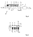
Fig. 1 shows a schematic view of a first embodiment of a PWM amplifier according to the invention, with a first MEMS switch in cross-section, -
Fig. 2 is a schematic top view of the MEMS switch shown infig. 1 , -
Fig. 3 shows a schematic view of a second embodiment of a PWM amplifier according to the invention, with a second MEMS switch in cross-section, -
Fig. 4 is a schematic top view of the MEMS switch shown infig. 3 , -
Fig. 5 shows a schematic view of a third embodiment of a PWM amplifier according to the invention, with a third MEMS switch in cross-section, -
Fig. 6 is a schematic top view of the MEMS switch shown infig. 5 , -
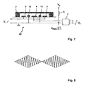
Fig. 7 shows a schematic view of a fourth embodiment of a PWM amplifier according to the invention, with a fourth MEMS switch in cross-section, and -
Fig. 8 is a graphic representation of the actuator signal for the MEMS switch shown infig. 7 . - Corresponding components are designated in the figures with the same reference numerals.
-
Fig. 1 shows anamplifier 10 with asubstrate 1 of for instance a slice of silicon with an insulating nitride layer, on which is arranged a MEMS switch formed by threeelectrodes leaf spring 2 of an electrically conductive, flexible material extending thereover.Leaf spring 2 is connected toearth 8 and can swing down under the influence of a voltage on theleft electrode 5 or themiddle electrode 3. By applying a triangular voltage Vm (the actuator voltage) to left electrode 5 (actuator electrode 5)leaf spring 2 periodically swings downward andleaf spring 5 is short-circuited with right electrode 4 (output electrode 4) when the voltage of triangular wave Vm becomes greater than the attraction voltage of the MEMS switch.Leaf spring 2 swings upward again on the downward flank of triangular wave Vm. Through the agency of an input signal to be amplified Vi, which is fed to middle electrode 3 (input electrode 3), the moment of downward swing can be moved forward by the extra attraction voltage oninput electrode 3. A direct voltage source Vp is connected tooutput electrode 4 via animpedance 6. Whenleaf spring 2 swings down, the circuit between the direct voltage source Vp to earth is short-circuited viaimpedance 6 and the conductor-conductor contact ofleaf spring 2, which results in a PWM square wave VPWM with considerable power which is modulated with the input signal. This PWM signal VPWM is supplied to a low-pass filter 7, the cut-off frequency of which is lower than the frequency of the actuator signal onactuator electrode 5, with the result that the input signal Vi fed toinput electrode 3 is recovered in amplified form as output signal Vo. Depending on the voltage supplied by direct voltage source Vp, the value ofimpedance 6 and the surface area of the contact betweenleaf spring 2 andoutput electrode 4, it is possible to realize a considerable power amplification, voltage amplification and/or current amplification.Input electrode 3 andactuator electrode 5 form the inputs of a comparator circuit in the shownamplifier 10. With respect to noise and for the purpose of an optimal power amplification, it is possible to consider adding a bias voltage to the input signal. It is also possible to replace the triangular voltage with a different periodic voltage in order to optimize the amplification and the noise. For the sake of clarity in the figure the signal forms occurring inamplifier 10 are shown schematically at the respective locations. -
Fig. 2 shows a schematic top view of the MEMS switch ofamplifier 10 offig. 1 by way of illustration of the layout of such a switch in an integrated circuit. -
Fig. 3 shows anamplifier 20 which differs fromamplifier 10 offig. 1 in thatoutput electrode 4 is provided on its contact surface with a dielectric 9, for instance of silicon nitride (SiNx) or tantalum oxide (Ta2O5), as a result of which the contact betweenleaf spring 2 andoutput electrode 4 is a capacitive contact. Connected via animpedance 6 tooutput electrode 4 is an alternating voltage source Vp, which for instance supplies a unipolar sine-wave signal Vp with a frequency well above the resonance frequency ofleaf spring 2. In this case the signal VPWM onoutput electrode 4 is an amplitude-modulated sine. If signal Vp is kept unipolar, it need not be rectified. Signal Vo at the output of low-pass filter 7 has the average value of unipolar sine Vp, which varies with input signal Vi. By way of alternative, a normal bipolar voltage Vp can also be fed tooutput electrode 4, in which case the output of low-pass filter 7 must be provided with an electronic or (micro-)mechanical rectifier diode. -
Fig. 4 shows a schematic top view of the MEMS switch ofamplifier 20 offig. 3 by way of illustration of the layout of such a switch in an integrated circuit. -
Fig. 5 shows anamplifier 30 which differs fromamplifier 20 offig. 3 in that a capacitive contact betweenleaf spring 2 andoutput electrode 4 is realized not by means of a dielectric, but by means of an air gap which occurs in the swung-down situation ofleaf spring 2 in that, using aspacer 11,leaf spring 2 supports on its underside on acorresponding spacer 12 onsubstrate 1. -
Fig. 6 shows a schematic top view of the MEMS switch ofamplifier 30 offig. 5 by way of illustration of the layout of such a switch in an integrated circuit. -
Fig. 7 shows anamplifier 40 which differs fromamplifier 30 offig. 5 in that the movablethin film 2 is embodied as a bridge which is supported at its two outer ends and which in the swung-down situation supports on two symmetrically placedspacers 12, input signal Vi is fed to two symmetrically arrangedinput electrodes 3, and a separate actuator electrode is omitted. The function of the actuator electrode in this circuit is fulfilled byoutput electrode 4, on which via impedance 6 a sine-wave signal Vp is supplied with a frequency higher than the resonance frequency ofbridge 2, which signal Vp is modulated with a triangular wave with a frequency just below the resonance frequency (shown infig. 8 ), so thatbridge 2 can follow the modulated signal but will only move with the effective value of the high-frequency sine-wave signal. At an input voltage Vi = 0V bridge 2 will be periodically swung downward and upward by the actuator signal Vp. The result hereof is that the capacitance value ofbridge 2 will change in accordance with a block-like pattern and that the high-frequency component of actuator signal Vp will be modulated with an additional square wave due to the presence ofimpedance 6. A direct voltage is obtained when the signal fromoutput electrode 4 is filtered with a low-pass filter 7 with a frequency lower than the modulation frequency of the actuator signal Vp. If the input voltage Vi > 0 V,bridge 2 will be swung downward sooner as a result of the increased attraction force onbridge 2, and will remain swung down for a longer part of a period of actuator signal Vp. The amplitude-modulated signal onoutput electrode 4 will now have a lower average value and the voltage will decrease after low-pass filter 7 as input voltage Vi increases. Because the output current depends on the capacity ofbridge 2 and the value ofimpedance 6, a power amplifier has thus been created. Depending on the parameters of the circuit and Vp, a voltage amplifier can also be obtained. The absence of a separate actuator electrode inamplifier circuit 40 provides the advantage that this circuit is smaller, easier to produce and can function at higher speeds. - Because resistors, capacitors and coils can be integrated in known and simple manner into a circuit with MEMS technology, it lies within the reach of the skilled person to integrate into one circuit the MEMS switch and the low-pass filter in an amplifier device according to the invention, for instance an operational amplifier or a high-power amplifier.
- It is emphasized that the above described exemplary embodiments serve to elucidate and not to limit the scope of the invention. It is possible for the skilled person to realize other embodiments within the inventive concept.
- The movable thin film in a MEMS switch in an amplifier according to the invention can for instance be realized as a leaf spring suspended from one outer end, as a bridge carried at two outer ends or as a membrane, which thin film can move in the plane as well as out of the plane of the substrate.
- The actuator means in a MEMS switch in a PWM amplifier according to the invention are described above as electrostatic drive means, although they can for instance also be realized in the form of electromagnetic or electrothermal drive means.
Claims (9)
- Amplifier device (10, 20, 30, 40) of the pulse width modulation amplifier type (PWM amplifier), comprising a switch according to a micro-electromechanical system (MEMS-switch) for a signal to be amplified (Vi), which MEMS switch comprises at least one substrate (1) on which are arranged- a movable thin film (2) of an electrically conductive material,- a first electrode (3) forming the input for the signal to be amplified (Vi),- a second electrode (4) forming the output for a pulse width-modulated signal (VPWM), and- actuator means (5, 6) for moving the thin film (2) subject to an actuator signal to be supplied (Vm, Vp) which is different from the signal to be amplified (Vi), and to the signal to be amplified (Vi),wherein the actuator signal to be supplied (Vm, Vp) is a periodic signal having a frequency chosen such that it is much higher than the frequency of the signal to be amplified (Vi), and
wherein the amplifier device is adapted to generate the pulse width-modulated signal (VPWM) subject to the movement of the thin film (2). - Amplifier device (10, 20, 30) as claimed in claim 1, wherein the actuator means (5) are formed by a third electrode (5) which is adapted as actuator electrode for supplying a modulator signal (Vm) thereon for the purpose of moving the thin film (2), wherein the first (3) and the third electrode (5) form the inputs of a comparator circuit.
- Amplifier device (10) as claimed in either of the claims 1-2, wherein the MEMS switch comprises a conductor-conductor contact of the thin film (2) and the second electrode (4).
- Amplifier device (20, 30, 40) as claimed in either of the claims 1-2, wherein the MEMS switch comprises a capacitive contact (9) of the thin film (2) and the second electrode (4).
- Amplifier device (30) as claimed in claim 4, wherein the capacitive contact is provided by an air gap between the thin film (2) and the second electrode (4), and the thin film (2) is provided on its side directed toward the substrate (1) with at least one spacer (11).
- Amplifier device (30, 40) as claimed in either of the claims 4-5, wherein the capacitive contact is provided by an air gap between the thin film (2) and the second electrode (4), and the substrate (1) is provided on its side directed toward the thin film (2) with at least one spacer (12).
- Amplifier device (10, 20, 30, 40) as claimed in any of the claims 1-6, wherein the electrically conductive material of the thin film (2) is selected from the group of aluminium (Al), polycrystalline silicon (Si), doped polycrystalline silicon, carbon (C), SiC, germanium (Ge), germanium-silicon alloys, titanium (Ti), titanium nitrides, nickel (Ni), copper (Cu), tantalum (Ta), tungsten (W), gold (Au) and stacks of at least two of these materials.
- Amplifier device as claimed in claim 1, wherein the actuator means are electromagnetic drive means.
- Amplifier device as claimed in claim 1, wherein the actuator means are electrothermal drive means.
Applications Claiming Priority (2)
| Application Number | Priority Date | Filing Date | Title |
|---|---|---|---|
| NL1034082A NL1034082C2 (en) | 2007-07-03 | 2007-07-03 | PWM amplifier. |
| PCT/NL2008/050422 WO2009005345A1 (en) | 2007-07-03 | 2008-06-26 | Pwm amplifier |
Publications (2)
| Publication Number | Publication Date |
|---|---|
| EP2162983A1 EP2162983A1 (en) | 2010-03-17 |
| EP2162983B1 true EP2162983B1 (en) | 2010-10-06 |
Family
ID=38687472
Family Applications (1)
| Application Number | Title | Priority Date | Filing Date |
|---|---|---|---|
| EP08766845A Not-in-force EP2162983B1 (en) | 2007-07-03 | 2008-06-26 | Pwm amplifier |
Country Status (6)
| Country | Link |
|---|---|
| US (1) | US20100253428A1 (en) |
| EP (1) | EP2162983B1 (en) |
| AT (1) | ATE484099T1 (en) |
| DE (1) | DE602008002941D1 (en) |
| NL (1) | NL1034082C2 (en) |
| WO (1) | WO2009005345A1 (en) |
Families Citing this family (1)
| Publication number | Priority date | Publication date | Assignee | Title |
|---|---|---|---|---|
| CN102170272B (en) * | 2010-02-25 | 2014-06-18 | 上海丽恒光微电子科技有限公司 | Power amplifier and bridge circuit thereof |
Family Cites Families (6)
| Publication number | Priority date | Publication date | Assignee | Title |
|---|---|---|---|---|
| US6674383B2 (en) * | 2000-11-01 | 2004-01-06 | Onix Microsystems, Inc. | PWM-based measurement interface for a micro-machined electrostatic actuator |
| DE102004037820A1 (en) * | 2004-08-04 | 2006-03-16 | Epcos Ag | Electrical circuit and component with the circuit |
| KR100659298B1 (en) * | 2005-01-04 | 2006-12-20 | 삼성전자주식회사 | MEMS switch and its manufacturing method |
| JP2006333437A (en) * | 2005-03-16 | 2006-12-07 | Taiyo Yuden Co Ltd | Digital amplifier and switching power source |
| US7319580B2 (en) * | 2005-03-29 | 2008-01-15 | Intel Corporation | Collapsing zipper varactor with inter-digit actuation electrodes for tunable filters |
| US7619469B2 (en) * | 2006-12-28 | 2009-11-17 | Alcatel-Lucent Usa Inc. | Current switched circuit for switch mode power amplifiers |
-
2007
- 2007-07-03 NL NL1034082A patent/NL1034082C2/en not_active IP Right Cessation
-
2008
- 2008-06-26 EP EP08766845A patent/EP2162983B1/en not_active Not-in-force
- 2008-06-26 US US12/665,566 patent/US20100253428A1/en not_active Abandoned
- 2008-06-26 DE DE602008002941T patent/DE602008002941D1/en active Active
- 2008-06-26 WO PCT/NL2008/050422 patent/WO2009005345A1/en not_active Ceased
- 2008-06-26 AT AT08766845T patent/ATE484099T1/en not_active IP Right Cessation
Also Published As
| Publication number | Publication date |
|---|---|
| DE602008002941D1 (en) | 2010-11-18 |
| US20100253428A1 (en) | 2010-10-07 |
| NL1034082C2 (en) | 2009-01-06 |
| EP2162983A1 (en) | 2010-03-17 |
| ATE484099T1 (en) | 2010-10-15 |
| WO2009005345A1 (en) | 2009-01-08 |
Similar Documents
| Publication | Publication Date | Title |
|---|---|---|
| US6593870B2 (en) | MEMS-based electrically isolated analog-to-digital converter | |
| US6232847B1 (en) | Trimmable singleband and tunable multiband integrated oscillator using micro-electromechanical system (MEMS) technology | |
| US6373007B1 (en) | Series and shunt mems RF switch | |
| JP5418607B2 (en) | Variable capacity device | |
| TW200428773A (en) | Boost circuit | |
| JP2000028462A (en) | Conversion device | |
| TW201145811A (en) | Variable class characteristic amplifier | |
| KR102070617B1 (en) | Micro electro mechanical systems am modulator and magnetic field sensor having the same | |
| JP4139422B2 (en) | module | |
| CN102804619A (en) | signal transmission device | |
| JP5338615B2 (en) | Variable capacitance device and method of driving variable capacitance element | |
| WO2023235228A1 (en) | Circuits and methods for generating a continuous current sense signal | |
| US10418961B2 (en) | Dual-mode filtering actuator driver apparatus, systems and methods | |
| CN115118312A (en) | Capacitive data transmission via galvanic isolation | |
| US20100253428A1 (en) | Pwm amplifier | |
| US20050270127A1 (en) | Micro-electromechanical switching device | |
| EP3915154B1 (en) | Semiconductor devices using semiconductor-metal phase change materials | |
| EP2878003B1 (en) | Switchable capacitor | |
| JP2023517620A (en) | Apparatus and method including amplifier circuit performing push-pull waveform shaping operation | |
| WO2009083891A2 (en) | Pulse-width modulated amplifier for inverted planar motor | |
| WO2017122602A1 (en) | Variable capacitor | |
| KR20050042814A (en) | Active method and system of establishing electrical contact | |
| Van Spengen et al. | The MEMSamp: using (RF-) MEMS switches for the micromechanical amplification of electronic signals | |
| Cagdaser et al. | Low-voltage electrostatic actuation with inherent position feedback | |
| WO2021190955A1 (en) | Nanoplasma switch device for ultrafast switching |
Legal Events
| Date | Code | Title | Description |
|---|---|---|---|
| PUAI | Public reference made under article 153(3) epc to a published international application that has entered the european phase |
Free format text: ORIGINAL CODE: 0009012 |
|
| 17P | Request for examination filed |
Effective date: 20091210 |
|
| AK | Designated contracting states |
Kind code of ref document: A1 Designated state(s): AT BE BG CH CY CZ DE DK EE ES FI FR GB GR HR HU IE IS IT LI LT LU LV MC MT NL NO PL PT RO SE SI SK TR |
|
| AX | Request for extension of the european patent |
Extension state: AL BA MK RS |
|
| GRAP | Despatch of communication of intention to grant a patent |
Free format text: ORIGINAL CODE: EPIDOSNIGR1 |
|
| GRAS | Grant fee paid |
Free format text: ORIGINAL CODE: EPIDOSNIGR3 |
|
| GRAA | (expected) grant |
Free format text: ORIGINAL CODE: 0009210 |
|
| AK | Designated contracting states |
Kind code of ref document: B1 Designated state(s): AT BE BG CH CY CZ DE DK EE ES FI FR GB GR HR HU IE IS IT LI LT LU LV MC MT NL NO PL PT RO SE SI SK TR |
|
| REG | Reference to a national code |
Ref country code: GB Ref legal event code: FG4D |
|
| REG | Reference to a national code |
Ref country code: CH Ref legal event code: EP |
|
| REG | Reference to a national code |
Ref country code: IE Ref legal event code: FG4D |
|
| REF | Corresponds to: |
Ref document number: 602008002941 Country of ref document: DE Date of ref document: 20101118 Kind code of ref document: P |
|
| REG | Reference to a national code |
Ref country code: NL Ref legal event code: T3 |
|
| PG25 | Lapsed in a contracting state [announced via postgrant information from national office to epo] |
Ref country code: SI Free format text: LAPSE BECAUSE OF FAILURE TO SUBMIT A TRANSLATION OF THE DESCRIPTION OR TO PAY THE FEE WITHIN THE PRESCRIBED TIME-LIMIT Effective date: 20101006 |
|
| LTIE | Lt: invalidation of european patent or patent extension |
Effective date: 20101006 |
|
| PG25 | Lapsed in a contracting state [announced via postgrant information from national office to epo] |
Ref country code: LT Free format text: LAPSE BECAUSE OF FAILURE TO SUBMIT A TRANSLATION OF THE DESCRIPTION OR TO PAY THE FEE WITHIN THE PRESCRIBED TIME-LIMIT Effective date: 20101006 Ref country code: NO Free format text: LAPSE BECAUSE OF FAILURE TO SUBMIT A TRANSLATION OF THE DESCRIPTION OR TO PAY THE FEE WITHIN THE PRESCRIBED TIME-LIMIT Effective date: 20110106 |
|
| PG25 | Lapsed in a contracting state [announced via postgrant information from national office to epo] |
Ref country code: BG Free format text: LAPSE BECAUSE OF FAILURE TO SUBMIT A TRANSLATION OF THE DESCRIPTION OR TO PAY THE FEE WITHIN THE PRESCRIBED TIME-LIMIT Effective date: 20110106 Ref country code: SE Free format text: LAPSE BECAUSE OF FAILURE TO SUBMIT A TRANSLATION OF THE DESCRIPTION OR TO PAY THE FEE WITHIN THE PRESCRIBED TIME-LIMIT Effective date: 20101006 Ref country code: HR Free format text: LAPSE BECAUSE OF FAILURE TO SUBMIT A TRANSLATION OF THE DESCRIPTION OR TO PAY THE FEE WITHIN THE PRESCRIBED TIME-LIMIT Effective date: 20101006 Ref country code: PT Free format text: LAPSE BECAUSE OF FAILURE TO SUBMIT A TRANSLATION OF THE DESCRIPTION OR TO PAY THE FEE WITHIN THE PRESCRIBED TIME-LIMIT Effective date: 20110207 Ref country code: AT Free format text: LAPSE BECAUSE OF FAILURE TO SUBMIT A TRANSLATION OF THE DESCRIPTION OR TO PAY THE FEE WITHIN THE PRESCRIBED TIME-LIMIT Effective date: 20101006 Ref country code: LV Free format text: LAPSE BECAUSE OF FAILURE TO SUBMIT A TRANSLATION OF THE DESCRIPTION OR TO PAY THE FEE WITHIN THE PRESCRIBED TIME-LIMIT Effective date: 20101006 Ref country code: IS Free format text: LAPSE BECAUSE OF FAILURE TO SUBMIT A TRANSLATION OF THE DESCRIPTION OR TO PAY THE FEE WITHIN THE PRESCRIBED TIME-LIMIT Effective date: 20110206 Ref country code: FI Free format text: LAPSE BECAUSE OF FAILURE TO SUBMIT A TRANSLATION OF THE DESCRIPTION OR TO PAY THE FEE WITHIN THE PRESCRIBED TIME-LIMIT Effective date: 20101006 |
|
| PG25 | Lapsed in a contracting state [announced via postgrant information from national office to epo] |
Ref country code: GR Free format text: LAPSE BECAUSE OF FAILURE TO SUBMIT A TRANSLATION OF THE DESCRIPTION OR TO PAY THE FEE WITHIN THE PRESCRIBED TIME-LIMIT Effective date: 20110107 Ref country code: BE Free format text: LAPSE BECAUSE OF FAILURE TO SUBMIT A TRANSLATION OF THE DESCRIPTION OR TO PAY THE FEE WITHIN THE PRESCRIBED TIME-LIMIT Effective date: 20101006 |
|
| PG25 | Lapsed in a contracting state [announced via postgrant information from national office to epo] |
Ref country code: EE Free format text: LAPSE BECAUSE OF FAILURE TO SUBMIT A TRANSLATION OF THE DESCRIPTION OR TO PAY THE FEE WITHIN THE PRESCRIBED TIME-LIMIT Effective date: 20101006 Ref country code: CZ Free format text: LAPSE BECAUSE OF FAILURE TO SUBMIT A TRANSLATION OF THE DESCRIPTION OR TO PAY THE FEE WITHIN THE PRESCRIBED TIME-LIMIT Effective date: 20101006 Ref country code: ES Free format text: LAPSE BECAUSE OF FAILURE TO SUBMIT A TRANSLATION OF THE DESCRIPTION OR TO PAY THE FEE WITHIN THE PRESCRIBED TIME-LIMIT Effective date: 20110117 |
|
| PLBE | No opposition filed within time limit |
Free format text: ORIGINAL CODE: 0009261 |
|
| STAA | Information on the status of an ep patent application or granted ep patent |
Free format text: STATUS: NO OPPOSITION FILED WITHIN TIME LIMIT |
|
| PG25 | Lapsed in a contracting state [announced via postgrant information from national office to epo] |
Ref country code: SK Free format text: LAPSE BECAUSE OF FAILURE TO SUBMIT A TRANSLATION OF THE DESCRIPTION OR TO PAY THE FEE WITHIN THE PRESCRIBED TIME-LIMIT Effective date: 20101006 Ref country code: RO Free format text: LAPSE BECAUSE OF FAILURE TO SUBMIT A TRANSLATION OF THE DESCRIPTION OR TO PAY THE FEE WITHIN THE PRESCRIBED TIME-LIMIT Effective date: 20101006 Ref country code: DK Free format text: LAPSE BECAUSE OF FAILURE TO SUBMIT A TRANSLATION OF THE DESCRIPTION OR TO PAY THE FEE WITHIN THE PRESCRIBED TIME-LIMIT Effective date: 20101006 Ref country code: PL Free format text: LAPSE BECAUSE OF FAILURE TO SUBMIT A TRANSLATION OF THE DESCRIPTION OR TO PAY THE FEE WITHIN THE PRESCRIBED TIME-LIMIT Effective date: 20101006 |
|
| 26N | No opposition filed |
Effective date: 20110707 |
|
| REG | Reference to a national code |
Ref country code: DE Ref legal event code: R097 Ref document number: 602008002941 Country of ref document: DE Effective date: 20110707 |
|
| PG25 | Lapsed in a contracting state [announced via postgrant information from national office to epo] |
Ref country code: MT Free format text: LAPSE BECAUSE OF FAILURE TO SUBMIT A TRANSLATION OF THE DESCRIPTION OR TO PAY THE FEE WITHIN THE PRESCRIBED TIME-LIMIT Effective date: 20101006 Ref country code: IT Free format text: LAPSE BECAUSE OF FAILURE TO SUBMIT A TRANSLATION OF THE DESCRIPTION OR TO PAY THE FEE WITHIN THE PRESCRIBED TIME-LIMIT Effective date: 20101006 |
|
| REG | Reference to a national code |
Ref country code: IE Ref legal event code: MM4A |
|
| PG25 | Lapsed in a contracting state [announced via postgrant information from national office to epo] |
Ref country code: IE Free format text: LAPSE BECAUSE OF NON-PAYMENT OF DUE FEES Effective date: 20110626 |
|
| REG | Reference to a national code |
Ref country code: CH Ref legal event code: PL |
|
| REG | Reference to a national code |
Ref country code: CH Ref legal event code: PL |
|
| PG25 | Lapsed in a contracting state [announced via postgrant information from national office to epo] |
Ref country code: LI Free format text: LAPSE BECAUSE OF NON-PAYMENT OF DUE FEES Effective date: 20120630 Ref country code: MC Free format text: LAPSE BECAUSE OF NON-PAYMENT OF DUE FEES Effective date: 20110630 Ref country code: CH Free format text: LAPSE BECAUSE OF NON-PAYMENT OF DUE FEES Effective date: 20120630 |
|
| PG25 | Lapsed in a contracting state [announced via postgrant information from national office to epo] |
Ref country code: CY Free format text: LAPSE BECAUSE OF EXPIRATION OF PROTECTION Effective date: 20101006 Ref country code: LU Free format text: LAPSE BECAUSE OF NON-PAYMENT OF DUE FEES Effective date: 20110626 |
|
| PGFP | Annual fee paid to national office [announced via postgrant information from national office to epo] |
Ref country code: GB Payment date: 20130625 Year of fee payment: 6 Ref country code: DE Payment date: 20130617 Year of fee payment: 6 |
|
| PGFP | Annual fee paid to national office [announced via postgrant information from national office to epo] |
Ref country code: NL Payment date: 20130624 Year of fee payment: 6 Ref country code: FR Payment date: 20130703 Year of fee payment: 6 |
|
| PG25 | Lapsed in a contracting state [announced via postgrant information from national office to epo] |
Ref country code: TR Free format text: LAPSE BECAUSE OF FAILURE TO SUBMIT A TRANSLATION OF THE DESCRIPTION OR TO PAY THE FEE WITHIN THE PRESCRIBED TIME-LIMIT Effective date: 20101006 |
|
| PG25 | Lapsed in a contracting state [announced via postgrant information from national office to epo] |
Ref country code: HU Free format text: LAPSE BECAUSE OF FAILURE TO SUBMIT A TRANSLATION OF THE DESCRIPTION OR TO PAY THE FEE WITHIN THE PRESCRIBED TIME-LIMIT Effective date: 20101006 |
|
| REG | Reference to a national code |
Ref country code: DE Ref legal event code: R119 Ref document number: 602008002941 Country of ref document: DE |
|
| REG | Reference to a national code |
Ref country code: NL Ref legal event code: V1 Effective date: 20150101 |
|
| GBPC | Gb: european patent ceased through non-payment of renewal fee |
Effective date: 20140626 |
|
| REG | Reference to a national code |
Ref country code: DE Ref legal event code: R119 Ref document number: 602008002941 Country of ref document: DE Effective date: 20150101 |
|
| REG | Reference to a national code |
Ref country code: FR Ref legal event code: ST Effective date: 20150227 |
|
| PG25 | Lapsed in a contracting state [announced via postgrant information from national office to epo] |
Ref country code: NL Free format text: LAPSE BECAUSE OF NON-PAYMENT OF DUE FEES Effective date: 20150101 |
|
| PG25 | Lapsed in a contracting state [announced via postgrant information from national office to epo] |
Ref country code: DE Free format text: LAPSE BECAUSE OF NON-PAYMENT OF DUE FEES Effective date: 20150101 |
|
| PG25 | Lapsed in a contracting state [announced via postgrant information from national office to epo] |
Ref country code: GB Free format text: LAPSE BECAUSE OF NON-PAYMENT OF DUE FEES Effective date: 20140626 Ref country code: FR Free format text: LAPSE BECAUSE OF NON-PAYMENT OF DUE FEES Effective date: 20140630 |