EP2160683B1 - Cache for a multi thread and multi core system and methods thereof - Google Patents
Cache for a multi thread and multi core system and methods thereof Download PDFInfo
- Publication number
- EP2160683B1 EP2160683B1 EP08771309.5A EP08771309A EP2160683B1 EP 2160683 B1 EP2160683 B1 EP 2160683B1 EP 08771309 A EP08771309 A EP 08771309A EP 2160683 B1 EP2160683 B1 EP 2160683B1
- Authority
- EP
- European Patent Office
- Prior art keywords
- data
- cache
- request
- instruction
- thread
- Prior art date
- Legal status (The legal status is an assumption and is not a legal conclusion. Google has not performed a legal analysis and makes no representation as to the accuracy of the status listed.)
- Not-in-force
Links
Images


Classifications
-
- G—PHYSICS
- G06—COMPUTING OR CALCULATING; COUNTING
- G06F—ELECTRIC DIGITAL DATA PROCESSING
- G06F12/00—Accessing, addressing or allocating within memory systems or architectures
- G06F12/02—Addressing or allocation; Relocation
- G06F12/08—Addressing or allocation; Relocation in hierarchically structured memory systems, e.g. virtual memory systems
- G06F12/0802—Addressing of a memory level in which the access to the desired data or data block requires associative addressing means, e.g. caches
- G06F12/0844—Multiple simultaneous or quasi-simultaneous cache accessing
- G06F12/0855—Overlapped cache accessing, e.g. pipeline
- G06F12/0859—Overlapped cache accessing, e.g. pipeline with reload from main memory
Definitions
- the present disclosure relates to a cache for improving performance of a processor, and, more particularly, to a cache for a multi-threaded and/or multicore system for improving the performance of the cache of the processor.
- United States Patent US 6195748 B1 (Chrysos et al. ), concerns apparatus for sampling instruction execution information in a processor pipeline.
- additional bits of a register are used to store the identifier of a thread, process identifier, address space number, CPU number, and instruction number.
- Out-of-order superscalar microprocessors are utilised to reschedule instructions according to data and resource which may be accomplished using information regarding the resource utilization of threads.
- Information about resource utilizations of threads can be used in a multithreaded processor to schedule threads so as to maximize overall resource utilization and throughput.
- United States Patent Application Publication US 2005/0289142 A1 concerns a system and method for previewing the relevance of streaming data.
- the system output of this system shows the degree of relevance and locations of relevant portions in streaming data using colour intensity.
- a relevance bar graphically displays the relevance of the current data stream with the top of the bar displaying the relevance of the current position in the data stream and the relevance of future events in the data stream displayed further down the bar. In the bar, higher intensity colour indicates higher relevance.
- a colour bar may be used to indicate to a user the relevance of a currently viewed data stream and the relevance of future portions of the data stream.
- a visual indicator may be provided to illustrate the relevance of a data stream to the query and/or subject.
- each execution unit may be configured to handle out-of-order returns.
- the EU's may provide, with each instruction fetch request, the instruction queue location to place the cache line once it returns. Since each thread may have, for example, 3 cachelines of buffering, a 2b code may be sufficient. This is indicated in Figure 2 as IQ[1:0] for instruction queue address[1:0]. Further, the request may be for the odd instruction in a cacheline such as the case of an unaligned jump address. This signal is indicated in Figure 2 as"O/E" signaling 'odd' or 'even'.
- the cache architecture described herein may discard head-of-queue at issue time since each issue is guaranteed to complete (i.e., it may not need to re-issue) and any routing or meta data may be carried with the request, there may not be a block on the head of a queue, thus no need to flatten the queues to expose all entries.
- the maximum depth of an instruction buffer may be a performance decision, limited only by the total number of destinations in an execution unit's instruction FIFO. For example, this may be limited to 12 (i.e., 4 threads/EU x 3 cache lines deep/inst-buffer).
- a cache hit may be forwarded to a hit FIFO 242, the depth of which may be a performance/cost decision. With a finite depth, the FIFO may fill up on occasion. Tracking the current depth of the FIFO 242 is the hit-FIFO tracking circuitry, which may consist of some combinatorial logic as well as an adder or other circuitry. Each time an issue occurs, the hit/miss outcome is unknown , and the adder may take a conservative route and assume a hit. It therefore adds 1 to its current value. If the result is later determined to be a miss, the adder may subtract 1. The adder may also subtract one for each entry removed from the FIFO and forwarded to the cache RAM.
- Cachelines returned from the hit path may be for a single thread.
- a small amount of logic may be present to synthesize the 16 channel IQ O/E signaling, with only the proper thread enabled, to the bypass MUX.
- the output interface of the cache 112 to each Execution Unit (EU) may be provided with separate data valid bit returned to each EU for each EU/thread/instruction-queue-entry/color permutation to allow the returned data to be indicated as valid simultaneously to all possible destination locations provided in the EU implementation.
- the in-flight RAM 214 storage is changed to store the set attribute and the way attribute. Accordingly, the architecture of the cache 112 may provide the access of the plurality of data to a plurality of requests in a single clock. Further, the overall performance of the cache 112 is improved compared to the typical cache implementation.
- the arbiter 220 may be used for scheduling data return to the EUs. On any given clock, data from either a hit or a miss or both may be ready for return. In some embodiments, an arbitration algorithm may be used to determine the rules as to which data-return to service.
- FIG. 3 is a flow diagram illustrating a method for improving the performance of the processor.
- the method may include storing a plurality of data in a data Random Access Memory (RAM) (302).
- the method may further include holding information for all outstanding requests forwarded to a next-level memory subsystem (304).
- the method may also include clearing information associated with a serviced request after the request has been fulfilled (306).
- the method may additionally include determining if a subsequent request matches an address supplied to one or more requests already in-flight to the next-level memory subsystem (308).
- the method may further include matching fulfilled requests serviced by the next-level memory subsystem to at least one requestor who issued requests while an original request was in-flight to the next level memory subsystem (310).
- the method may also include storing information specific to each request, the information including a set attribute and a way attribute, the set and way attributes configured to identify where the returned data should be held in the data RAM once the data is returned, the information specific to each request further including thread ID and color (312).
- the method may additionally include scheduling hit and miss data returns (314).
Landscapes
- Engineering & Computer Science (AREA)
- Theoretical Computer Science (AREA)
- Physics & Mathematics (AREA)
- General Engineering & Computer Science (AREA)
- General Physics & Mathematics (AREA)
- Memory System Of A Hierarchy Structure (AREA)
Description
- The present disclosure relates to a cache for improving performance of a processor, and, more particularly, to a cache for a multi-threaded and/or multicore system for improving the performance of the cache of the processor.
- United States Patent
US 6195748 B1 (Chrysos et al. ), concerns apparatus for sampling instruction execution information in a processor pipeline. In this apparatus, additional bits of a register are used to store the identifier of a thread, process identifier, address space number, CPU number, and instruction number. Out-of-order superscalar microprocessors are utilised to reschedule instructions according to data and resource which may be accomplished using information regarding the resource utilization of threads. Information about resource utilizations of threads can be used in a multithreaded processor to schedule threads so as to maximize overall resource utilization and throughput. - United States Patent Application Publication
US 2005/0289142 A1 concerns a system and method for previewing the relevance of streaming data. The system output of this system shows the degree of relevance and locations of relevant portions in streaming data using colour intensity. A relevance bar graphically displays the relevance of the current data stream with the top of the bar displaying the relevance of the current position in the data stream and the relevance of future events in the data stream displayed further down the bar. In the bar, higher intensity colour indicates higher relevance. Based on a subject and/or a query, a colour bar may be used to indicate to a user the relevance of a currently viewed data stream and the relevance of future portions of the data stream. A visual indicator may be provided to illustrate the relevance of a data stream to the query and/or subject. - The advantages and features of the present disclosure will become better understood with reference to the following detailed description and claims taken in conjunction with the accompanying drawings, wherein like elements are identified with like symbols, and in which:
-
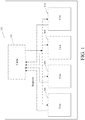
FIG. 1 is a block diagram illustrating a multi thread and multi core system for improving the performance of a processor, according to an exemplary embodiment of the present disclosure; -
FIG. 2 is a block diagram illustrating an architecture of a cache, according to an exemplary embodiment of the present disclosure; and -
FIG. 3 is a flow diagram illustrating a method for improving the performance of a cache of a processor, according to an exemplary embodiment of the present disclosure. - For a thorough understanding of the present disclosure, refer to the following detailed description, including the appended claims, in connection with the above-described drawings. Although the present disclosure is described in connection with exemplary embodiments, the disclosure is not intended to be limited to the specific forms set forth herein. Also, it is to be understood that the phraseology and terminology used herein is for the purpose of description and should not be regarded as limiting.
- The terms "first," "second," and the like, herein do not denote any order, quantity, or importance, but rather are used to distinguish one element from another. The terms "a" and "an" herein do not denote a limitation of quantity, but rather denote the presence of at least one of the referenced item.
-
FIG. 1 is a block diagram illustrating a multi-thread andmulti core system 102 for improving the performance of a processor. The system may include a plurality ofcores cache 112 connected to the plurality ofcores cache 112 may support the plurality ofcores cache 112. The plurality ofcores cache 112 is described below in detail in conjunction withFIG. 2 . -
FIG. 2 is a block diagram 200 illustrating architecture of thecache 112. Thecache 112 may include a plurality ofinstruction queues tag RAM 212; an in-flight RAM 214; and anarbiter 220. The plurality ofinstruction queues data RAM 210 may be capable of storing a plurality of data of various forms.Arbiter 220 may indicate the point at which hit and miss data returning to each execution unit may collide and need arbitration so as to honor any limitations of the receiving units, such as sending only one response back per clock cycle. - In some embodiments, each execution unit (EU) may be configured to handle out-of-order returns. The EU's may provide, with each instruction fetch request, the instruction queue location to place the cache line once it returns. Since each thread may have, for example, 3 cachelines of buffering, a 2b code may be sufficient. This is indicated in
Figure 2 as IQ[1:0] for instruction queue address[1:0]. Further, the request may be for the odd instruction in a cacheline such as the case of an unaligned jump address. This signal is indicated inFigure 2 as"O/E" signaling 'odd' or 'even'. - In some embodiments, there may be 1 instruction queue per execution unit. The cache architecture described herein may discard head-of-queue at issue time since each issue is guaranteed to complete (i.e., it may not need to re-issue) and any routing or meta data may be carried with the request, there may not be a block on the head of a queue, thus no need to flatten the queues to expose all entries. The maximum depth of an instruction buffer may be a performance decision, limited only by the total number of destinations in an execution unit's instruction FIFO. For example, this may be limited to 12 (i.e., 4 threads/EU x 3 cache lines deep/inst-buffer).
- The
tag RAM 212 may be configured for storing the memory addresses of the plurality of data stored in thedata RAM 210. Thetag RAM 212 may identify data from a memory, which is currently stored in thedata RAM 210. The memory addresses stored in thetag RAM 212 may determine whether a cache lookup results in a hit or a miss. The size of thetag RAM 212 may be proportional to the capacity and organization of thedata RAM 112. - In some embodiments, the tag may take more than one clock to compare and update. For example, 3 clocks may be used. Thus, there is the potential for a given issue to hit a tag that may change due to a previous miss, but which has not yet been written to the
tag RAM 212. A copy of the set addresses issued during the last 3 clocks may be stored (e.g., in registers located to the right of arbiter inFigure 2 ) and compared against each head of queue. This may require a plurality of comparators in parallel, shown inFigure 2 as tag in-flight logic 240. If there is a match between a queue's head and only one of the sets issued in the last 3 clocks, that queue may be blocked from arbitration. - A cache hit may be forwarded to a hit FIFO 242, the depth of which may be a performance/cost decision. With a finite depth, the FIFO may fill up on occasion. Tracking the current depth of the
FIFO 242 is the hit-FIFO tracking circuitry, which may consist of some combinatorial logic as well as an adder or other circuitry. Each time an issue occurs, the hit/miss outcome is unknown , and the adder may take a conservative route and assume a hit. It therefore adds 1 to its current value. If the result is later determined to be a miss, the adder may subtract 1. The adder may also subtract one for each entry removed from the FIFO and forwarded to the cache RAM. Since a forward and mispredicted hit may occur in the same clock, the capability to subtract 2 may be supported. Cachelines returned from the hit path may be for a single thread. A small amount of logic may be present to synthesize the 16 channel IQ O/E signaling, with only the proper thread enabled, to the bypass MUX. - A cache miss may be forwarded to miss-
logic 244. This circuitry may maintain for each cache line, the EU instruction queue positions waiting on that linefill. This information may be held in the in-flight RAM 214 (e.g., 128 entries, one per cacheline). The width of the RAM may vary. For each miss, the in-flight RAM 214 may be queried for the set/way. If there are no outstanding requests for that line, then the miss may be forwarded to the miss queue, and the thread's position in the RAM may be updated to show the thread waiting on the linefill. If query indicates one or more may already be in flight then the miss may be squashed and the thread's position updated. Miss data may return via fill logic which may see all cacheline returns from the L2. For each return a look-up may be performed for the associated set in the In-flight RAM 214, indicating all requesting EUs waiting a fill for that cacheline of data. The cacheline data and control indicating all pending fills to EU and instruction queue positions may be sent to the instruction bus. The bypass mux arbiter may join hit and miss fills and drive the instruction bus. It may service miss returns over hit returns. In some embodiments a miss return may cause back pressure on the hit queue. - The in-
flight RAM 214 may be configured to maintain identification and accounting information for all outstanding misses at any instant. Identification may consist of determining which thread and execution unit (EU) made the request, the destination location, corresponding to the set and way, to place the eventual returned data in the data RAM, and a color indicator which may identify which sequential stream from the requesting thread/EU the request belongs to. When the caches starts to process a request, the requested address may be checked in thetag RAM 212 and if a match is not found (i.e. results in a miss) the request may be forwarded to the in-flight RAM 214 and its supporting logic. TheRAM 214 and logic may compare the address of the new miss request against the subset of addresses (typically mapping to the same cache set) of all outstanding requests which have the potential to match as held in the in-flight RAM 214. If a match exists, a request corresponding to that address has already been forward to the next level memory subsystem by a previous miss (i.e. the request is already in-flight), and the new miss request and its associated identification and accounting information are logged into the in-flight RAM 214, and no request is made of the next level memory subsystem. If a match is not found, indicating that there is not an outstanding request to the next level memory subsystem for this address, the misses identification and accounting information are logged into the in-flight RAM 214 and the request may be forwarded to the next-level memory subsystem. Once the next-level memory subsystem has fulfilled a miss request provided by this cache, it may return the requested data and either the requested address and/or associated accounting information, based on implementation choice. The address/accounting information may be compared to the subset potential matches (typically mapping to the same set) held in the in-flight RAM 214 contents in an effort to find one or more matches. The set of matches found may indicate the list of EU/thread combinations that had requested this same data. The in-flight RAM 214 and its associated logic may broadcast instruction data to a plurality of threads in the plurality ofcores flight RAM 214 and all pending threads waiting for the instruction data may be acknowledged in a single clock. Thus, the architecture of thecache 112 provides access of the instruction data to the plurality of threads. - The output interface of the
cache 112 to each Execution Unit (EU) may be provided with separate data valid bit returned to each EU for each EU/thread/instruction-queue-entry/color permutation to allow the returned data to be indicated as valid simultaneously to all possible destination locations provided in the EU implementation. Further, the in-flight RAM 214 storage is changed to store the set attribute and the way attribute. Accordingly, the architecture of thecache 112 may provide the access of the plurality of data to a plurality of requests in a single clock. Further, the overall performance of thecache 112 is improved compared to the typical cache implementation. - The interface of the
cache 112 with EU comprises a color bit to allow the EU to prefetch an instruction ahead of the point of its execution in a speculative manner, and later when data is returned, identify if the returned data is valid or stale. To accomplish this, a "color bit", i.e. a multi-state variable, may be used identify the current and arbitrary "color" associated with the current sequential instruction stream being executed by a thread. In some embodiments, color may be maintained per thread per EU. The value of the color bit may be changed whenever a discontinuity in the instruction request stream is encountered as the EU executes instructions, for example in the case of a 'jump' instruction. The color information may be sent to the cache as part of any cache request. Thecache 112 described herein may support handling two colors per thread, although this may be easily extended to handle 'n' colors. The EU provides a color bit with each request made of the cache, and the cache maintains the color bit with all accounting information held while the request is being serviced. Upon return of the data by the cache to the EU, the cache may return the value of the color bit which was sent as part of the original request. This allows the EU/thread to compare the returned color with the execution unit's (EU) current color maintained locally. A color-match indicates that the EU is still operating on the sequential instruction stream in effect when the request was made to the cache, and thus the returned data may be relevant to the instruction stream being executed; a mis-match may indicate that the EU/thread has encountered an instruction stream discontinuity during the time the request was outstanding, and thus the returned data may not be relevant to the current stream of execution and may be discarded. This mechanism allows EU/thread to make speculative instruction requests with a new color at every instruction stream discontinuity, even though there may be outstanding and potentially stale requests pending for a same thread in thecache 112. This may improve the overall performance of thecache 112 having large kernels causing low hit ratio by determining at data-return time the validity of the returned data. - The
arbiter 220 may be used for scheduling data return to the EUs. On any given clock, data from either a hit or a miss or both may be ready for return. In some embodiments, an arbitration algorithm may be used to determine the rules as to which data-return to service. -
FIG. 3 is a flow diagram illustrating a method for improving the performance of the processor. The method may include storing a plurality of data in a data Random Access Memory (RAM) (302). The method may further include holding information for all outstanding requests forwarded to a next-level memory subsystem (304). The method may also include clearing information associated with a serviced request after the request has been fulfilled (306). The method may additionally include determining if a subsequent request matches an address supplied to one or more requests already in-flight to the next-level memory subsystem (308). The method may further include matching fulfilled requests serviced by the next-level memory subsystem to at least one requestor who issued requests while an original request was in-flight to the next level memory subsystem (310). The method may also include storing information specific to each request, the information including a set attribute and a way attribute, the set and way attributes configured to identify where the returned data should be held in the data RAM once the data is returned, the information specific to each request further including thread ID and color (312). The method may additionally include scheduling hit and miss data returns (314). - The foregoing descriptions of specific embodiments of the present disclosure have been presented for purposes of illustration and description. They are not intended to be exhaustive or to limit the disclosure to the precise forms disclosed, many modifications and variations are possible in light of the above teaching. The embodiments were chosen and described in order to best explain the principles of the disclosure and its practical application, to thereby enable others skilled in the art to best utilize the disclosure.
Claims (14)
- A cache (112) for a processor, the cache comprising:a plurality of instruction queues (202, 204, 206, 208) configured to handle at least one out-of-order instruction return;a data Random Access Memory "RAM" (210) capable of storing a plurality of data;a tag RAM (212) capable of storing memory addresses and data of the plurality of data stored in the data RAM (210);an in-flight RAM (214) capable ofholding (304) information for all outstanding requests forwarded to a next-level memory subsystem;clearing (306) information associated with a serviced request after the request has been fulfilled;determining (308) if a subsequent request matches an address supplied to one or more requests already in-flight to the next-level memory subsystem;matching (310) fulfilled requests serviced by the next-level memory subsystem to at least one requestor who issued requests while an original request was in-flight to the next-level memory subsystem; andstoring (312) information specific to each request, the information including a set attribute and a way attribute, the set and way attributes configured to identify where the returned data should be held in the data RAM once the data is returned, the information specific to each request further including thread ID, instruction queue position and a colour indicator, wherein the colour indicator is a multi-state variable and used to identify a sequential stream in a requesting thread that made the request to the cache and wherein the colour indicator allows the requesting thread to determine whether the returned data is valid or stale, wherein the identification of the sequential stream allows an Execution Unit "EU"/thread to make speculative instruction requests, prefetch instructions ahead of the point of their execution, with a new colour at every instruction stream, wherein a colour-match indicates that the EU is still operating on the sequential instruction stream when the request was made to the cache, and the returned data is relevant to the instruction stream being executed; and wherein a mis-match in colour indicates that the EU/thread has encountered an instruction stream discontinuity during the time the request was outstanding, and the returned data is not relevant to the current stream of execution and may be discarded, allowing the EU/thread to make speculative instruction requests with a new colour at every instruction stream discontinuity; andan arbiter (220) for scheduling hit and miss data returns.
- The cache of claim 1, wherein the cache is capable of providing access to the plurality of data stored in the data RAM to a plurality of cores.
- The cache of claim 1, wherein the data RAM is effective to reduce a latency of the plurality of data stored in the data RAM (210).
- The cache (112) of claim 1, wherein at least one of the thread ID, instruction queue position and colour indicator is supplied back to the requestor once the request is fulfilled.
- The cache (112) of claim 4, wherein the cache (112) is adapted to return data to a plurality of threads in a single clock time.
- The cache (112) of claim 1, further comprising an execution unit interface comprising a colour bit for determining the relevance of returned data at the time the data is returned.
- The cache (112) of claim 6, wherein the EU interface is effective to improve a performance of the cache of the processor having a low hit ratio.
- A multi core and a multi thread system (102), the system comprising:a plurality of cores (104,106,108 & 110); anda cache (112) connected to the plurality of cores, the cache being a cache as claimed in any one of the preceding claims.
- A method for improving performance of a cache (112) of a processor, the method comprising:storing (302) a plurality of data in a data Random Access Memory "RAM" (210);storing memory addresses of the plurality of data stored in the data RAM (210) in a tag RAM (212);holding (304) information for all outstanding requests forwarded to a next-level memory subsystem;clearing (306) information associated with a serviced request after the request has been fulfilled;determining (308) if a subsequent request matches an address supplied to one or more requests already in-flight to the next-level memory subsystem;matching (310) fulfilled requests serviced by the next-level memory subsystem to at least one requestor who issued requests while an original request was in-flight to the next-level memory subsystem;storing (312) information specific to each request, the information including a set attribute and a way attribute, the set and way attributes configured to identify where the returned data should be held in the data RAM (210) once the data is returned, the information specific to each request further including thread ID, instruction queue position and a colour indicator, wherein the colour indicator is a multi-state variable and used to identify a sequential stream in a requesting thread that made the request to the cache and wherein the colour indicator allows the requesting thread to determine whether the returned data is valid or stale, wherein the identification of the sequential stream allows an Execution Unit "EU"/thread to make speculative instruction requests, prefetch instructions ahead of the point of their execution, with a new colour at every instruction stream, wherein a colour-match indicates that the EU is still operating on the sequential instruction stream when the request was made to the cache, and the returned data is relevant to the instruction stream being executed; and wherein a mis-match in colour indicates that the EU/thread has encountered an instruction stream discontinuity during the time the request was outstanding and the returned data is not relevant to the current stream of execution and may be discarded, allowing the EU/thread to make speculative instruction requests with a new colour at every instruction stream discontinuity; andscheduling (314) hit and miss data returns.
- The method of claim 9, wherein the cache is capable of providing access of the plurality of data stored in the data RAM (210) to a plurality of cores (104,106,108 & 110).
- The method of claim 9, wherein the data RAM (210) reduces a latency of the plurality of data stored in the data RAM (210).
- The method of claim 9, wherein at least one of said thread ID, instruction queue position and colour indicator is supplied back to the requestor once the request is fulfilled
- The method of claim 12, wherein the cache (112) provides access of the instruction data to a plurality of threads in a single clock time.
- The method of claim 9, further comprising an end user interface comprising a colour bit for reducing a latency in case of a jump instruction.
Applications Claiming Priority (2)
| Application Number | Priority Date | Filing Date | Title |
|---|---|---|---|
| US11/770,120 US8171225B2 (en) | 2007-06-28 | 2007-06-28 | Cache for a multi thread and multi core system and methods thereof |
| PCT/US2008/067279 WO2009006018A2 (en) | 2007-06-28 | 2008-06-18 | Cache for a multi thread and multi core system and methods thereof |
Publications (3)
| Publication Number | Publication Date |
|---|---|
| EP2160683A2 EP2160683A2 (en) | 2010-03-10 |
| EP2160683A4 EP2160683A4 (en) | 2011-07-06 |
| EP2160683B1 true EP2160683B1 (en) | 2018-08-01 |
Family
ID=40162105
Family Applications (1)
| Application Number | Title | Priority Date | Filing Date |
|---|---|---|---|
| EP08771309.5A Not-in-force EP2160683B1 (en) | 2007-06-28 | 2008-06-18 | Cache for a multi thread and multi core system and methods thereof |
Country Status (5)
| Country | Link |
|---|---|
| US (1) | US8171225B2 (en) |
| EP (1) | EP2160683B1 (en) |
| JP (1) | JP5118199B2 (en) |
| CN (1) | CN101730885B (en) |
| WO (1) | WO2009006018A2 (en) |
Families Citing this family (24)
| Publication number | Priority date | Publication date | Assignee | Title |
|---|---|---|---|---|
| IL127569A0 (en) | 1998-09-16 | 1999-10-28 | Comsense Technologies Ltd | Interactive toys |
| US20100030838A1 (en) * | 1998-08-27 | 2010-02-04 | Beepcard Ltd. | Method to use acoustic signals for computer communications |
| US6607136B1 (en) * | 1998-09-16 | 2003-08-19 | Beepcard Inc. | Physical presence digital authentication system |
| CA2345745A1 (en) * | 1998-10-02 | 2000-04-13 | Comsense Technologies, Ltd. | Card for interaction with a computer |
| US8019609B2 (en) | 1999-10-04 | 2011-09-13 | Dialware Inc. | Sonic/ultrasonic authentication method |
| US9219708B2 (en) * | 2001-03-22 | 2015-12-22 | DialwareInc. | Method and system for remotely authenticating identification devices |
| US8171225B2 (en) | 2007-06-28 | 2012-05-01 | Intel Corporation | Cache for a multi thread and multi core system and methods thereof |
| KR101647818B1 (en) * | 2010-04-13 | 2016-08-12 | 삼성전자주식회사 | Apparatus for routing data between multicore and method thereof |
| CN102087634B (en) * | 2011-01-27 | 2012-10-03 | 凌阳科技股份有限公司 | Device and method for improving cache hit rate |
| CN104158764B (en) * | 2014-08-12 | 2018-02-06 | 新华三技术有限公司 | Message processing method and device |
| JP5917678B1 (en) * | 2014-12-26 | 2016-05-18 | 株式会社Pfu | Information processing apparatus, method, and program |
| US10031834B2 (en) | 2016-08-31 | 2018-07-24 | Microsoft Technology Licensing, Llc | Cache-based tracing for time travel debugging and analysis |
| US10042737B2 (en) | 2016-08-31 | 2018-08-07 | Microsoft Technology Licensing, Llc | Program tracing for time travel debugging and analysis |
| US10310977B2 (en) * | 2016-10-20 | 2019-06-04 | Microsoft Technology Licensing, Llc | Facilitating recording a trace file of code execution using a processor cache |
| US10489273B2 (en) | 2016-10-20 | 2019-11-26 | Microsoft Technology Licensing, Llc | Reuse of a related thread's cache while recording a trace file of code execution |
| US10324851B2 (en) | 2016-10-20 | 2019-06-18 | Microsoft Technology Licensing, Llc | Facilitating recording a trace file of code execution using way-locking in a set-associative processor cache |
| US10310963B2 (en) | 2016-10-20 | 2019-06-04 | Microsoft Technology Licensing, Llc | Facilitating recording a trace file of code execution using index bits in a processor cache |
| US10540250B2 (en) | 2016-11-11 | 2020-01-21 | Microsoft Technology Licensing, Llc | Reducing storage requirements for storing memory addresses and values |
| CN108255517B (en) * | 2016-12-29 | 2020-05-05 | 展讯通信(上海)有限公司 | Processor and method for requesting instruction cache data |
| US10318332B2 (en) | 2017-04-01 | 2019-06-11 | Microsoft Technology Licensing, Llc | Virtual machine execution tracing |
| US10296442B2 (en) | 2017-06-29 | 2019-05-21 | Microsoft Technology Licensing, Llc | Distributed time-travel trace recording and replay |
| FR3086409A1 (en) * | 2018-09-26 | 2020-03-27 | Stmicroelectronics (Grenoble 2) Sas | METHOD FOR MANAGING THE PROVISION OF INFORMATION, PARTICULARLY INSTRUCTIONS, TO A MICROPROCESSOR AND CORRESPONDING SYSTEM |
| US10877894B2 (en) * | 2019-05-16 | 2020-12-29 | Micron Technology, Inc. | Memory-side transaction context memory interface systems and methods, wherein first context and first address are communicated on plural wires during different clock cycles and second context (of block of the first context) is communicated on additional wire during one of the different clock cycles |
| CN117130662A (en) * | 2023-09-19 | 2023-11-28 | 摩尔线程智能科技(北京)有限责任公司 | An instruction reading method and L2 instruction cache, electronic device and storage medium |
Family Cites Families (16)
| Publication number | Priority date | Publication date | Assignee | Title |
|---|---|---|---|---|
| JPS61220047A (en) * | 1985-03-27 | 1986-09-30 | Hitachi Ltd | Memory control system |
| JP2596637B2 (en) * | 1990-11-09 | 1997-04-02 | 株式会社日立製作所 | Cache control method |
| JP3729832B2 (en) * | 1992-02-28 | 2005-12-21 | 沖電気工業株式会社 | Cache memory device |
| US6195748B1 (en) * | 1997-11-26 | 2001-02-27 | Compaq Computer Corporation | Apparatus for sampling instruction execution information in a processor pipeline |
| US6549930B1 (en) * | 1997-11-26 | 2003-04-15 | Compaq Computer Corporation | Method for scheduling threads in a multithreaded processor |
| US6141732A (en) * | 1998-03-24 | 2000-10-31 | Novell, Inc. | Burst-loading of instructions into processor cache by execution of linked jump instructions embedded in cache line size blocks |
| US6473832B1 (en) * | 1999-05-18 | 2002-10-29 | Advanced Micro Devices, Inc. | Load/store unit having pre-cache and post-cache queues for low latency load memory operations |
| JP2002312238A (en) * | 2001-04-18 | 2002-10-25 | Hitachi Ltd | Cache control unit |
| JP2003122632A (en) * | 2001-10-17 | 2003-04-25 | Nec Corp | Cache data registering system and registering method |
| JP2003256274A (en) * | 2002-03-04 | 2003-09-10 | Kyocera Corp | High-speed data processing apparatus and control method thereof |
| US6990557B2 (en) * | 2002-06-04 | 2006-01-24 | Sandbridge Technologies, Inc. | Method and apparatus for multithreaded cache with cache eviction based on thread identifier |
| US7228520B1 (en) * | 2004-01-30 | 2007-06-05 | Xilinx, Inc. | Method and apparatus for a programmable interface of a soft platform on a programmable logic device |
| US8438157B2 (en) * | 2004-06-28 | 2013-05-07 | International Business Machines Corporation | System and method for previewing relevance of streaming data |
| JP4575065B2 (en) * | 2004-07-29 | 2010-11-04 | 富士通株式会社 | Cache memory control device, cache memory control method, central processing unit, information processing device, central control method |
| US20060143401A1 (en) * | 2004-12-27 | 2006-06-29 | Jacob Doweck | Method and apparatus for prefetching based on cache fill buffer hits |
| US8171225B2 (en) | 2007-06-28 | 2012-05-01 | Intel Corporation | Cache for a multi thread and multi core system and methods thereof |
-
2007
- 2007-06-28 US US11/770,120 patent/US8171225B2/en not_active Expired - Fee Related
-
2008
- 2008-06-18 EP EP08771309.5A patent/EP2160683B1/en not_active Not-in-force
- 2008-06-18 JP JP2010514977A patent/JP5118199B2/en not_active Expired - Fee Related
- 2008-06-18 WO PCT/US2008/067279 patent/WO2009006018A2/en not_active Ceased
- 2008-06-18 CN CN2008800222067A patent/CN101730885B/en not_active Expired - Fee Related
Non-Patent Citations (1)
| Title |
|---|
| None * |
Also Published As
| Publication number | Publication date |
|---|---|
| JP5118199B2 (en) | 2013-01-16 |
| JP2010532057A (en) | 2010-09-30 |
| US8171225B2 (en) | 2012-05-01 |
| CN101730885B (en) | 2013-03-27 |
| CN101730885A (en) | 2010-06-09 |
| EP2160683A2 (en) | 2010-03-10 |
| WO2009006018A3 (en) | 2009-03-05 |
| US20090006729A1 (en) | 2009-01-01 |
| EP2160683A4 (en) | 2011-07-06 |
| WO2009006018A2 (en) | 2009-01-08 |
Similar Documents
| Publication | Publication Date | Title |
|---|---|---|
| US8171225B2 (en) | Cache for a multi thread and multi core system and methods thereof | |
| US6898694B2 (en) | High instruction fetch bandwidth in multithread processor using temporary instruction cache to deliver portion of cache line in subsequent clock cycle | |
| US8667225B2 (en) | Store aware prefetching for a datastream | |
| US6681295B1 (en) | Fast lane prefetching | |
| JP3670039B2 (en) | Super scalar microprocessor | |
| EP3060983B1 (en) | Bandwidth increase in branch prediction unit and level 1 instruction cache | |
| US6393536B1 (en) | Load/store unit employing last-in-buffer indication for rapid load-hit-store | |
| US7962724B1 (en) | Branch loop performance enhancement | |
| US6266744B1 (en) | Store to load forwarding using a dependency link file | |
| US7873785B2 (en) | Multi-core multi-thread processor | |
| US9009445B2 (en) | Memory management unit speculative hardware table walk scheme | |
| US5774710A (en) | Cache line branch prediction scheme that shares among sets of a set associative cache | |
| US11132202B2 (en) | Cache control circuitry and methods | |
| US20170139706A1 (en) | Optimizing thread selection at fetch, select, and commit stages of processor core pipeline | |
| US20030065897A1 (en) | Method and apparatus for reordering memory requests for page coherency | |
| US8006073B1 (en) | Simultaneous speculative threading light mode | |
| US7370152B2 (en) | Memory controller with prefetching capability | |
| US20030074530A1 (en) | Load/store unit with fast memory data access mechanism | |
| CN100397365C (en) | Device and method for solving deadlock extraction condition in branch target address cache | |
| TWI283827B (en) | Apparatus and method for efficiently updating branch target address cache | |
| US10452400B2 (en) | Multi-thread processor with multi-bank branch-target buffer | |
| US6772297B2 (en) | Cache controlling device and processor | |
| CN112579170B (en) | Processor and method for reducing virtual address calculation | |
| US10303483B2 (en) | Arithmetic processing unit and control method for arithmetic processing unit | |
| CN122018983A (en) | General purpose processor instruction fetch apparatus and method |
Legal Events
| Date | Code | Title | Description |
|---|---|---|---|
| PUAI | Public reference made under article 153(3) epc to a published international application that has entered the european phase |
Free format text: ORIGINAL CODE: 0009012 |
|
| 17P | Request for examination filed |
Effective date: 20091127 |
|
| AK | Designated contracting states |
Kind code of ref document: A2 Designated state(s): AT BE BG CH CY CZ DE DK EE ES FI FR GB GR HR HU IE IS IT LI LT LU LV MC MT NL NO PL PT RO SE SI SK TR |
|
| AX | Request for extension of the european patent |
Extension state: AL BA MK RS |
|
| A4 | Supplementary search report drawn up and despatched |
Effective date: 20110608 |
|
| 17Q | First examination report despatched |
Effective date: 20110628 |
|
| DAX | Request for extension of the european patent (deleted) | ||
| STAA | Information on the status of an ep patent application or granted ep patent |
Free format text: STATUS: EXAMINATION IS IN PROGRESS |
|
| GRAP | Despatch of communication of intention to grant a patent |
Free format text: ORIGINAL CODE: EPIDOSNIGR1 |
|
| STAA | Information on the status of an ep patent application or granted ep patent |
Free format text: STATUS: GRANT OF PATENT IS INTENDED |
|
| INTG | Intention to grant announced |
Effective date: 20180226 |
|
| GRAS | Grant fee paid |
Free format text: ORIGINAL CODE: EPIDOSNIGR3 |
|
| GRAA | (expected) grant |
Free format text: ORIGINAL CODE: 0009210 |
|
| STAA | Information on the status of an ep patent application or granted ep patent |
Free format text: STATUS: THE PATENT HAS BEEN GRANTED |
|
| AK | Designated contracting states |
Kind code of ref document: B1 Designated state(s): AT BE BG CH CY CZ DE DK EE ES FI FR GB GR HR HU IE IS IT LI LT LU LV MC MT NL NO PL PT RO SE SI SK TR |
|
| REG | Reference to a national code |
Ref country code: GB Ref legal event code: FG4D |
|
| REG | Reference to a national code |
Ref country code: CH Ref legal event code: EP Ref country code: AT Ref legal event code: REF Ref document number: 1025103 Country of ref document: AT Kind code of ref document: T Effective date: 20180815 |
|
| REG | Reference to a national code |
Ref country code: IE Ref legal event code: FG4D |
|
| REG | Reference to a national code |
Ref country code: DE Ref legal event code: R096 Ref document number: 602008056258 Country of ref document: DE |
|
| REG | Reference to a national code |
Ref country code: NL Ref legal event code: MP Effective date: 20180801 |
|
| REG | Reference to a national code |
Ref country code: LT Ref legal event code: MG4D |
|
| REG | Reference to a national code |
Ref country code: AT Ref legal event code: MK05 Ref document number: 1025103 Country of ref document: AT Kind code of ref document: T Effective date: 20180801 |
|
| PG25 | Lapsed in a contracting state [announced via postgrant information from national office to epo] |
Ref country code: FI Free format text: LAPSE BECAUSE OF FAILURE TO SUBMIT A TRANSLATION OF THE DESCRIPTION OR TO PAY THE FEE WITHIN THE PRESCRIBED TIME-LIMIT Effective date: 20180801 Ref country code: IS Free format text: LAPSE BECAUSE OF FAILURE TO SUBMIT A TRANSLATION OF THE DESCRIPTION OR TO PAY THE FEE WITHIN THE PRESCRIBED TIME-LIMIT Effective date: 20181201 Ref country code: NO Free format text: LAPSE BECAUSE OF FAILURE TO SUBMIT A TRANSLATION OF THE DESCRIPTION OR TO PAY THE FEE WITHIN THE PRESCRIBED TIME-LIMIT Effective date: 20181101 Ref country code: GR Free format text: LAPSE BECAUSE OF FAILURE TO SUBMIT A TRANSLATION OF THE DESCRIPTION OR TO PAY THE FEE WITHIN THE PRESCRIBED TIME-LIMIT Effective date: 20181102 Ref country code: BG Free format text: LAPSE BECAUSE OF FAILURE TO SUBMIT A TRANSLATION OF THE DESCRIPTION OR TO PAY THE FEE WITHIN THE PRESCRIBED TIME-LIMIT Effective date: 20181101 Ref country code: NL Free format text: LAPSE BECAUSE OF FAILURE TO SUBMIT A TRANSLATION OF THE DESCRIPTION OR TO PAY THE FEE WITHIN THE PRESCRIBED TIME-LIMIT Effective date: 20180801 Ref country code: AT Free format text: LAPSE BECAUSE OF FAILURE TO SUBMIT A TRANSLATION OF THE DESCRIPTION OR TO PAY THE FEE WITHIN THE PRESCRIBED TIME-LIMIT Effective date: 20180801 Ref country code: SE Free format text: LAPSE BECAUSE OF FAILURE TO SUBMIT A TRANSLATION OF THE DESCRIPTION OR TO PAY THE FEE WITHIN THE PRESCRIBED TIME-LIMIT Effective date: 20180801 Ref country code: LT Free format text: LAPSE BECAUSE OF FAILURE TO SUBMIT A TRANSLATION OF THE DESCRIPTION OR TO PAY THE FEE WITHIN THE PRESCRIBED TIME-LIMIT Effective date: 20180801 Ref country code: PL Free format text: LAPSE BECAUSE OF FAILURE TO SUBMIT A TRANSLATION OF THE DESCRIPTION OR TO PAY THE FEE WITHIN THE PRESCRIBED TIME-LIMIT Effective date: 20180801 |
|
| PG25 | Lapsed in a contracting state [announced via postgrant information from national office to epo] |
Ref country code: ES Free format text: LAPSE BECAUSE OF FAILURE TO SUBMIT A TRANSLATION OF THE DESCRIPTION OR TO PAY THE FEE WITHIN THE PRESCRIBED TIME-LIMIT Effective date: 20180801 Ref country code: LV Free format text: LAPSE BECAUSE OF FAILURE TO SUBMIT A TRANSLATION OF THE DESCRIPTION OR TO PAY THE FEE WITHIN THE PRESCRIBED TIME-LIMIT Effective date: 20180801 Ref country code: HR Free format text: LAPSE BECAUSE OF FAILURE TO SUBMIT A TRANSLATION OF THE DESCRIPTION OR TO PAY THE FEE WITHIN THE PRESCRIBED TIME-LIMIT Effective date: 20180801 |
|
| PG25 | Lapsed in a contracting state [announced via postgrant information from national office to epo] |
Ref country code: RO Free format text: LAPSE BECAUSE OF FAILURE TO SUBMIT A TRANSLATION OF THE DESCRIPTION OR TO PAY THE FEE WITHIN THE PRESCRIBED TIME-LIMIT Effective date: 20180801 Ref country code: CZ Free format text: LAPSE BECAUSE OF FAILURE TO SUBMIT A TRANSLATION OF THE DESCRIPTION OR TO PAY THE FEE WITHIN THE PRESCRIBED TIME-LIMIT Effective date: 20180801 Ref country code: IT Free format text: LAPSE BECAUSE OF FAILURE TO SUBMIT A TRANSLATION OF THE DESCRIPTION OR TO PAY THE FEE WITHIN THE PRESCRIBED TIME-LIMIT Effective date: 20180801 Ref country code: EE Free format text: LAPSE BECAUSE OF FAILURE TO SUBMIT A TRANSLATION OF THE DESCRIPTION OR TO PAY THE FEE WITHIN THE PRESCRIBED TIME-LIMIT Effective date: 20180801 |
|
| REG | Reference to a national code |
Ref country code: DE Ref legal event code: R097 Ref document number: 602008056258 Country of ref document: DE |
|
| PG25 | Lapsed in a contracting state [announced via postgrant information from national office to epo] |
Ref country code: DK Free format text: LAPSE BECAUSE OF FAILURE TO SUBMIT A TRANSLATION OF THE DESCRIPTION OR TO PAY THE FEE WITHIN THE PRESCRIBED TIME-LIMIT Effective date: 20180801 Ref country code: SK Free format text: LAPSE BECAUSE OF FAILURE TO SUBMIT A TRANSLATION OF THE DESCRIPTION OR TO PAY THE FEE WITHIN THE PRESCRIBED TIME-LIMIT Effective date: 20180801 |
|
| PLBE | No opposition filed within time limit |
Free format text: ORIGINAL CODE: 0009261 |
|
| STAA | Information on the status of an ep patent application or granted ep patent |
Free format text: STATUS: NO OPPOSITION FILED WITHIN TIME LIMIT |
|
| 26N | No opposition filed |
Effective date: 20190503 |
|
| PG25 | Lapsed in a contracting state [announced via postgrant information from national office to epo] |
Ref country code: SI Free format text: LAPSE BECAUSE OF FAILURE TO SUBMIT A TRANSLATION OF THE DESCRIPTION OR TO PAY THE FEE WITHIN THE PRESCRIBED TIME-LIMIT Effective date: 20180801 |
|
| PG25 | Lapsed in a contracting state [announced via postgrant information from national office to epo] |
Ref country code: MC Free format text: LAPSE BECAUSE OF FAILURE TO SUBMIT A TRANSLATION OF THE DESCRIPTION OR TO PAY THE FEE WITHIN THE PRESCRIBED TIME-LIMIT Effective date: 20180801 |
|
| REG | Reference to a national code |
Ref country code: CH Ref legal event code: PL |
|
| REG | Reference to a national code |
Ref country code: BE Ref legal event code: MM Effective date: 20190630 |
|
| PG25 | Lapsed in a contracting state [announced via postgrant information from national office to epo] |
Ref country code: TR Free format text: LAPSE BECAUSE OF FAILURE TO SUBMIT A TRANSLATION OF THE DESCRIPTION OR TO PAY THE FEE WITHIN THE PRESCRIBED TIME-LIMIT Effective date: 20180801 |
|
| PG25 | Lapsed in a contracting state [announced via postgrant information from national office to epo] |
Ref country code: IE Free format text: LAPSE BECAUSE OF NON-PAYMENT OF DUE FEES Effective date: 20190618 |
|
| PG25 | Lapsed in a contracting state [announced via postgrant information from national office to epo] |
Ref country code: CH Free format text: LAPSE BECAUSE OF NON-PAYMENT OF DUE FEES Effective date: 20190630 Ref country code: LI Free format text: LAPSE BECAUSE OF NON-PAYMENT OF DUE FEES Effective date: 20190630 Ref country code: BE Free format text: LAPSE BECAUSE OF NON-PAYMENT OF DUE FEES Effective date: 20190630 Ref country code: LU Free format text: LAPSE BECAUSE OF NON-PAYMENT OF DUE FEES Effective date: 20190618 |
|
| PG25 | Lapsed in a contracting state [announced via postgrant information from national office to epo] |
Ref country code: FR Free format text: LAPSE BECAUSE OF NON-PAYMENT OF DUE FEES Effective date: 20190630 Ref country code: PT Free format text: LAPSE BECAUSE OF FAILURE TO SUBMIT A TRANSLATION OF THE DESCRIPTION OR TO PAY THE FEE WITHIN THE PRESCRIBED TIME-LIMIT Effective date: 20181201 |
|
| PGFP | Annual fee paid to national office [announced via postgrant information from national office to epo] |
Ref country code: DE Payment date: 20200602 Year of fee payment: 13 |
|
| PGFP | Annual fee paid to national office [announced via postgrant information from national office to epo] |
Ref country code: GB Payment date: 20200610 Year of fee payment: 13 |
|
| PG25 | Lapsed in a contracting state [announced via postgrant information from national office to epo] |
Ref country code: CY Free format text: LAPSE BECAUSE OF FAILURE TO SUBMIT A TRANSLATION OF THE DESCRIPTION OR TO PAY THE FEE WITHIN THE PRESCRIBED TIME-LIMIT Effective date: 20180801 |
|
| PG25 | Lapsed in a contracting state [announced via postgrant information from national office to epo] |
Ref country code: MT Free format text: LAPSE BECAUSE OF FAILURE TO SUBMIT A TRANSLATION OF THE DESCRIPTION OR TO PAY THE FEE WITHIN THE PRESCRIBED TIME-LIMIT Effective date: 20180801 Ref country code: HU Free format text: LAPSE BECAUSE OF FAILURE TO SUBMIT A TRANSLATION OF THE DESCRIPTION OR TO PAY THE FEE WITHIN THE PRESCRIBED TIME-LIMIT; INVALID AB INITIO Effective date: 20080618 |
|
| REG | Reference to a national code |
Ref country code: DE Ref legal event code: R119 Ref document number: 602008056258 Country of ref document: DE |
|
| GBPC | Gb: european patent ceased through non-payment of renewal fee |
Effective date: 20210618 |
|
| PG25 | Lapsed in a contracting state [announced via postgrant information from national office to epo] |
Ref country code: GB Free format text: LAPSE BECAUSE OF NON-PAYMENT OF DUE FEES Effective date: 20210618 Ref country code: DE Free format text: LAPSE BECAUSE OF NON-PAYMENT OF DUE FEES Effective date: 20220101 |