EP2159853A2 - Light source device with hollow metal reflector - Google Patents
Light source device with hollow metal reflector Download PDFInfo
- Publication number
- EP2159853A2 EP2159853A2 EP09167801A EP09167801A EP2159853A2 EP 2159853 A2 EP2159853 A2 EP 2159853A2 EP 09167801 A EP09167801 A EP 09167801A EP 09167801 A EP09167801 A EP 09167801A EP 2159853 A2 EP2159853 A2 EP 2159853A2
- Authority
- EP
- European Patent Office
- Prior art keywords
- light source
- source device
- reflector
- circuit board
- solid state
- Prior art date
- Legal status (The legal status is an assumption and is not a legal conclusion. Google has not performed a legal analysis and makes no representation as to the accuracy of the status listed.)
- Withdrawn
Links
- 229910052751 metal Inorganic materials 0.000 title claims abstract description 8
- 239000002184 metal Substances 0.000 title claims abstract description 8
- 239000007787 solid Substances 0.000 claims abstract description 29
- OAICVXFJPJFONN-UHFFFAOYSA-N Phosphorus Chemical compound [P] OAICVXFJPJFONN-UHFFFAOYSA-N 0.000 claims description 13
- 239000008393 encapsulating agent Substances 0.000 claims description 10
- 239000002245 particle Substances 0.000 claims description 5
- JNDMLEXHDPKVFC-UHFFFAOYSA-N aluminum;oxygen(2-);yttrium(3+) Chemical compound [O-2].[O-2].[O-2].[Al+3].[Y+3] JNDMLEXHDPKVFC-UHFFFAOYSA-N 0.000 claims description 4
- 229910019901 yttrium aluminum garnet Inorganic materials 0.000 claims description 4
- BPQQTUXANYXVAA-UHFFFAOYSA-N Orthosilicate Chemical compound [O-][Si]([O-])([O-])[O-] BPQQTUXANYXVAA-UHFFFAOYSA-N 0.000 claims description 2
- FNCIDSNKNZQJTJ-UHFFFAOYSA-N alumane;terbium Chemical compound [AlH3].[Tb] FNCIDSNKNZQJTJ-UHFFFAOYSA-N 0.000 claims description 2
- 239000002223 garnet Substances 0.000 claims description 2
- 239000000463 material Substances 0.000 claims description 2
- 150000004767 nitrides Chemical class 0.000 claims description 2
- 239000004020 conductor Substances 0.000 description 12
- 230000017525 heat dissipation Effects 0.000 description 7
- 239000011230 binding agent Substances 0.000 description 2
- TWNQGVIAIRXVLR-UHFFFAOYSA-N oxo(oxoalumanyloxy)alumane Chemical compound O=[Al]O[Al]=O TWNQGVIAIRXVLR-UHFFFAOYSA-N 0.000 description 2
- RYGMFSIKBFXOCR-UHFFFAOYSA-N Copper Chemical compound [Cu] RYGMFSIKBFXOCR-UHFFFAOYSA-N 0.000 description 1
- XUIMIQQOPSSXEZ-UHFFFAOYSA-N Silicon Chemical compound [Si] XUIMIQQOPSSXEZ-UHFFFAOYSA-N 0.000 description 1
- 238000009825 accumulation Methods 0.000 description 1
- 239000000956 alloy Substances 0.000 description 1
- 229910045601 alloy Inorganic materials 0.000 description 1
- 229910052782 aluminium Inorganic materials 0.000 description 1
- XAGFODPZIPBFFR-UHFFFAOYSA-N aluminium Chemical compound [Al] XAGFODPZIPBFFR-UHFFFAOYSA-N 0.000 description 1
- 229910010293 ceramic material Inorganic materials 0.000 description 1
- 238000011109 contamination Methods 0.000 description 1
- 229910052802 copper Inorganic materials 0.000 description 1
- 239000010949 copper Substances 0.000 description 1
- 230000006866 deterioration Effects 0.000 description 1
- 238000010292 electrical insulation Methods 0.000 description 1
- 239000003822 epoxy resin Substances 0.000 description 1
- 239000000203 mixture Substances 0.000 description 1
- 230000003287 optical effect Effects 0.000 description 1
- 230000002093 peripheral effect Effects 0.000 description 1
- 229920000647 polyepoxide Polymers 0.000 description 1
- 239000004065 semiconductor Substances 0.000 description 1
- 229910052710 silicon Inorganic materials 0.000 description 1
- 239000010703 silicon Substances 0.000 description 1
- 229920002050 silicone resin Polymers 0.000 description 1
- 239000000758 substrate Substances 0.000 description 1
- 239000012780 transparent material Substances 0.000 description 1
Images

Classifications
-
- H—ELECTRICITY
- H10—SEMICONDUCTOR DEVICES; ELECTRIC SOLID-STATE DEVICES NOT OTHERWISE PROVIDED FOR
- H10H—INORGANIC LIGHT-EMITTING SEMICONDUCTOR DEVICES HAVING POTENTIAL BARRIERS
- H10H20/00—Individual inorganic light-emitting semiconductor devices having potential barriers, e.g. light-emitting diodes [LED]
- H10H20/80—Constructional details
- H10H20/85—Packages
- H10H20/855—Optical field-shaping means, e.g. lenses
- H10H20/856—Reflecting means
-
- H—ELECTRICITY
- H10—SEMICONDUCTOR DEVICES; ELECTRIC SOLID-STATE DEVICES NOT OTHERWISE PROVIDED FOR
- H10H—INORGANIC LIGHT-EMITTING SEMICONDUCTOR DEVICES HAVING POTENTIAL BARRIERS
- H10H20/00—Individual inorganic light-emitting semiconductor devices having potential barriers, e.g. light-emitting diodes [LED]
- H10H20/80—Constructional details
- H10H20/85—Packages
- H10H20/858—Means for heat extraction or cooling
- H10H20/8582—Means for heat extraction or cooling characterised by their shape
-
- H—ELECTRICITY
- H10—SEMICONDUCTOR DEVICES; ELECTRIC SOLID-STATE DEVICES NOT OTHERWISE PROVIDED FOR
- H10H—INORGANIC LIGHT-EMITTING SEMICONDUCTOR DEVICES HAVING POTENTIAL BARRIERS
- H10H20/00—Individual inorganic light-emitting semiconductor devices having potential barriers, e.g. light-emitting diodes [LED]
- H10H20/80—Constructional details
- H10H20/85—Packages
- H10H20/852—Encapsulations
- H10H20/853—Encapsulations characterised by their shape
-
- H—ELECTRICITY
- H10—SEMICONDUCTOR DEVICES; ELECTRIC SOLID-STATE DEVICES NOT OTHERWISE PROVIDED FOR
- H10H—INORGANIC LIGHT-EMITTING SEMICONDUCTOR DEVICES HAVING POTENTIAL BARRIERS
- H10H20/00—Individual inorganic light-emitting semiconductor devices having potential barriers, e.g. light-emitting diodes [LED]
- H10H20/80—Constructional details
- H10H20/85—Packages
- H10H20/858—Means for heat extraction or cooling
- H10H20/8585—Means for heat extraction or cooling being an interconnection
Definitions
- the disclosure relates to light source devices with high heat-dissipation efficiency.
- LEDs Light emitting diodes
- the electrical and optical characteristics and lifespan of LEDs are affected by temperature conditions. High working temperatures can deteriorate the internal quantum efficiency of an LED and shorten its lifespan.
- the resistance of the semiconductor of an LED generates a negative temperature coefficient, and tends to be reduced with an increase in the working temperature. Such reduced resistance correspondingly results in stronger current at given voltages as well as the generation of excessive heat. If the excessive heat is not effectively dissipated, heat accumulation can lead to deterioration of the LED.
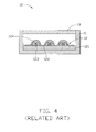
- a typical light source device 10 includes a shell 11, a light source module 12, and a cover 13.
- the light source module 12 is received in the shell 11.
- the cover 13 is located over and protects the light source module 12.
- the light source module 12 includes a printed circuit board 121, a circuit layer 122, a number of lighting elements 123 (such as LEDs), and an encapsulant 124.
- the circuit layer 122 and lighting elements 123 are mounted on the printed circuit board 121.
- the lighting elements 123 are electrically connected to the circuit layer 122.
- the encapsulant 124 is positioned on the printed circuit board 121 in discrete portions, so that each of the lighting elements 123 is packaged. Excessive heat from the light source module 12 can be dissipated through the shell 11. However, the thermal conductivity of the shell 11 is less than optimal, and the excessive heat is not necessarily effectively dissipated.
- FIG. 1 is an exploded view of a first exemplary embodiment of a light source device.
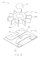
- FIG. 2 is an exploded view of a second exemplary embodiment of a light source device.
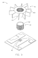
- FIG. 3 is an exploded view of a third exemplary embodiment of a light source device.
- FIG. 4 is a schematic cross-section of a typical light source device, in accordance with the related art.
- the light source device 20 includes a circuit board 21, a solid state lighting element 22, a reflector 23, and a light-pervious encapsulant 24.
- the circuit board 21 includes a first surface 210 and a second surface 212 at opposite main sides thereof.
- a circuit layer 214 is formed on the first surface 210 of the circuit board 21.
- the circuit board 21 may be made of aluminum oxide (Al 2 O 3 ), AIN, BeO, or other ceramic materials.
- the circuit board 21 may be a silicon substrate, a metal core printed circuit board (MCPCB), etc.
- the solid state lighting element 22 is a light emitting diode chip (LED chip), which is arranged on the first surface 210 of the circuit board 21 and electrically connected to the circuit layer 214.
- LED chip light emitting diode chip
- the reflector 23 has a hollow cylindrical or annular structure.
- the reflector 23 can be made of metal such as copper, aluminum or another suitable metal or alloy, so that the reflector 23 has good heat-dissipation efficiency.
- the reflector 23 is mounted on the first surface 210 of the circuit board 21 and surrounds the solid state lighting element 22.
- An inner peripheral surface 231 of the reflector 23 surrounding the solid state lighting element 22 reflects and directs light received from the solid state lighting element 22 towards a top side of the reflector 23, thereby changing a range of angles of light emission of the solid state lighting element 22.
- the reflector 23 may be connected to the circuit layer 214 via an insulating binder, so as to provide improved electrical insulation between the reflector 23 and the circuit board 21.
- the reflector 23 has good heat-dissipation efficiency, heat from the solid state lighting element 22 is effectively dissipated by the reflector 23 to the ambient environment. Thereby, the heat-dissipation efficiency of the light source device 20 is improved.
- the light-pervious encapsulant 24 is received in the hollow reflector 23 and covers the solid state lighting element 22, thereby protecting the solid state lighting element 22 from mechanical damage, moisture, and other ambient contamination.
- the light-pervious encapsulant 24 may be a condenser lens to collect light from the solid state lighting element 22 and redirect it upwards, such that the path of light emitted from the light source device 20 can be altered.
- the light-pervious encapsulant 24 may be made of epoxy resin, silicone resin, or another suitable electrically insulating transparent material.
- the light-pervious encapsulant 24 may further include a plurality of phosphor particles doped therein. For example, when the solid state lighting element 22 is a blue LED chip, the phosphor particles can include yellow phosphors.
- the yellow phosphors are excited by the blue light from the solid state lighting element 22 and emit yellow light.
- the yellow light and some of the original blue light combine (mix) to form white light, which emits from the light-pervious encapsulant 24.
- the phosphor particles may include yttrium aluminum garnet (YAG) phosphor, terbium aluminum garnet (TAG) phosphor, silicate phosphor, nitride phosphor, etc.
- a second exemplary embodiment of a light source device 30 is similar to the light source device 20.
- a plurality of fins 333 radially extends from an outer surface 332 of a reflector 33. Therefore a heat radiating area of the reflector 33 is increased, and a heat-dissipation efficiency of the light source device 30 is improved.
- the fins 333 may be connected to the circuit layer 214 via an insulating binder, so as to form an electrically insulated connection between the fins 333 and the circuit layer 214.
- the fins 333 may be isolated from the circuit layer 214 by air space.
- a third exemplary embodiment of a light source device 40 is similar to the light source device 20 of the first embodiment, except that the light source device 40 includes an inner reflector 43 and an outer heat conductor 45.
- the reflector 43 differs from the reflector 23 of the first embodiment in that an outer surface 432 of the reflector 43 has a screw thread thereon.
- the heat conductor 45 differs from the reflector 23 of the first embodiment as follows.
- An inner surface 451 of the heat conductor 45 has an inner screw thread thereon, and a plurality of fins 453 radially extends from an outer surface 452 of the heat conductor 45.
- the heat conductor 45 can be threadingly engaged with the reflector 43 to surround the reflector 43, if desired.
- the heat conductor 45 can be selectively omitted from the assembly of the light source device 40. Accordingly, the light source device 40 has flexibility to adapt to different application requirements.
- the heat conductor 45 and the reflector 43 have good heat-dissipation efficiency.
- the heat conductor 45 may be mechanically engaged with the reflector 43 in other ways.
- the heat conductor 45 may be coiled around the reflector 43, with an inner surface of the heat conductor 45 contacting an outer surface of the reflector 43.
- the heat conductor 45 is likewise detachably mounted to the reflector 43.
- the solid state lighting element 42 is a light emitting diode.
Landscapes
- Non-Portable Lighting Devices Or Systems Thereof (AREA)
- Arrangement Of Elements, Cooling, Sealing, Or The Like Of Lighting Devices (AREA)
- Led Device Packages (AREA)
Abstract
An exemplary light source device includes a circuit board (21), a solid state lighting element (22), and a hollow generally cylindrical metal reflector (23). The circuit board has a circuit layer (214) formed thereon. The solid state lighting element is mounted on the circuit board and electrically connected to the circuit layer. The reflector is mounted on the circuit board and insulated from the circuit layer. An inner surface (231) of the reflector surrounds the solid state lighting element and capable of reflecting and directing light from the solid state lighting element towards a side of the reflector far from the circuit board.
Description
- The disclosure relates to light source devices with high heat-dissipation efficiency.
- Light emitting diodes (LEDs) are easily influenced by temperature. Specifically, the electrical and optical characteristics and lifespan of LEDs are affected by temperature conditions. High working temperatures can deteriorate the internal quantum efficiency of an LED and shorten its lifespan. Furthermore, the resistance of the semiconductor of an LED generates a negative temperature coefficient, and tends to be reduced with an increase in the working temperature. Such reduced resistance correspondingly results in stronger current at given voltages as well as the generation of excessive heat. If the excessive heat is not effectively dissipated, heat accumulation can lead to deterioration of the LED.
- Referring to
FIG. 4 , a typicallight source device 10 includes ashell 11, alight source module 12, and acover 13. Thelight source module 12 is received in theshell 11. Thecover 13 is located over and protects thelight source module 12. Thelight source module 12 includes aprinted circuit board 121, acircuit layer 122, a number of lighting elements 123 (such as LEDs), and anencapsulant 124. Thecircuit layer 122 andlighting elements 123 are mounted on the printedcircuit board 121. Thelighting elements 123 are electrically connected to thecircuit layer 122. Theencapsulant 124 is positioned on the printedcircuit board 121 in discrete portions, so that each of thelighting elements 123 is packaged. Excessive heat from thelight source module 12 can be dissipated through theshell 11. However, the thermal conductivity of theshell 11 is less than optimal, and the excessive heat is not necessarily effectively dissipated. - Therefore, there is room for improvement within the art.
- Many aspects of the disclosure can be better understood with reference to the following drawings. The components in the drawings are not necessarily drawn to scale, the emphasis instead being placed upon clearly illustrating the principles of the disclosure. Moreover, in the drawings, all the views are schematic, and like reference numerals designate corresponding parts throughout certain of the views.
-
FIG. 1 is an exploded view of a first exemplary embodiment of a light source device. -
FIG. 2 is an exploded view of a second exemplary embodiment of a light source device. -
FIG. 3 is an exploded view of a third exemplary embodiment of a light source device. -
FIG. 4 is a schematic cross-section of a typical light source device, in accordance with the related art. - Referring to
FIG. 1 , a first embodiment of alight source device 20 is shown. Thelight source device 20 includes acircuit board 21, a solidstate lighting element 22, areflector 23, and a light-pervious encapsulant 24. - The
circuit board 21 includes afirst surface 210 and asecond surface 212 at opposite main sides thereof. Acircuit layer 214 is formed on thefirst surface 210 of thecircuit board 21. Thecircuit board 21 may be made of aluminum oxide (Al2O3), AIN, BeO, or other ceramic materials. Alternatively, thecircuit board 21 may be a silicon substrate, a metal core printed circuit board (MCPCB), etc. - In the illustrated embodiment, the solid
state lighting element 22 is a light emitting diode chip (LED chip), which is arranged on thefirst surface 210 of thecircuit board 21 and electrically connected to thecircuit layer 214. - The
reflector 23 has a hollow cylindrical or annular structure. Thereflector 23 can be made of metal such as copper, aluminum or another suitable metal or alloy, so that thereflector 23 has good heat-dissipation efficiency. Thereflector 23 is mounted on thefirst surface 210 of thecircuit board 21 and surrounds the solidstate lighting element 22. An innerperipheral surface 231 of thereflector 23 surrounding the solidstate lighting element 22 reflects and directs light received from the solidstate lighting element 22 towards a top side of thereflector 23, thereby changing a range of angles of light emission of the solidstate lighting element 22. Thereflector 23 may be connected to thecircuit layer 214 via an insulating binder, so as to provide improved electrical insulation between thereflector 23 and thecircuit board 21. Because thereflector 23 has good heat-dissipation efficiency, heat from the solidstate lighting element 22 is effectively dissipated by thereflector 23 to the ambient environment. Thereby, the heat-dissipation efficiency of thelight source device 20 is improved. - The light-
pervious encapsulant 24 is received in thehollow reflector 23 and covers the solidstate lighting element 22, thereby protecting the solidstate lighting element 22 from mechanical damage, moisture, and other ambient contamination. The light-pervious encapsulant 24 may be a condenser lens to collect light from the solidstate lighting element 22 and redirect it upwards, such that the path of light emitted from thelight source device 20 can be altered. The light-pervious encapsulant 24 may be made of epoxy resin, silicone resin, or another suitable electrically insulating transparent material. The light-pervious encapsulant 24 may further include a plurality of phosphor particles doped therein. For example, when the solidstate lighting element 22 is a blue LED chip, the phosphor particles can include yellow phosphors. The yellow phosphors are excited by the blue light from the solidstate lighting element 22 and emit yellow light. The yellow light and some of the original blue light combine (mix) to form white light, which emits from the light-pervious encapsulant 24. The phosphor particles may include yttrium aluminum garnet (YAG) phosphor, terbium aluminum garnet (TAG) phosphor, silicate phosphor, nitride phosphor, etc. - Referring to
FIG. 2 , a second exemplary embodiment of alight source device 30 is similar to thelight source device 20. However, in thelight source device 30, a plurality offins 333 radially extends from anouter surface 332 of areflector 33. Therefore a heat radiating area of thereflector 33 is increased, and a heat-dissipation efficiency of thelight source device 30 is improved. Thefins 333 may be connected to thecircuit layer 214 via an insulating binder, so as to form an electrically insulated connection between thefins 333 and thecircuit layer 214. Alternatively, thefins 333 may be isolated from thecircuit layer 214 by air space. - Referring to
FIG. 3 , a third exemplary embodiment of alight source device 40 is similar to thelight source device 20 of the first embodiment, except that thelight source device 40 includes aninner reflector 43 and anouter heat conductor 45. - The
reflector 43 differs from thereflector 23 of the first embodiment in that anouter surface 432 of thereflector 43 has a screw thread thereon. - The
heat conductor 45 differs from thereflector 23 of the first embodiment as follows. Aninner surface 451 of theheat conductor 45 has an inner screw thread thereon, and a plurality offins 453 radially extends from anouter surface 452 of theheat conductor 45. Thus theheat conductor 45 can be threadingly engaged with thereflector 43 to surround thereflector 43, if desired. Alternatively, theheat conductor 45 can be selectively omitted from the assembly of thelight source device 40. Accordingly, thelight source device 40 has flexibility to adapt to different application requirements. Theheat conductor 45 and thereflector 43 have good heat-dissipation efficiency. That is, heat from a solidstate lighting element 42 is effectively dissipated by thereflector 43 and theheat conductor 45 away from the solidstate lighting element 42, thereby improving the heat-dissipation efficiency of thelight source device 40. In alternative embodiments, theheat conductor 45 may be mechanically engaged with thereflector 43 in other ways. For example, theheat conductor 45 may be coiled around thereflector 43, with an inner surface of theheat conductor 45 contacting an outer surface of thereflector 43. With such alternative interengaging means, theheat conductor 45 is likewise detachably mounted to thereflector 43. In addition, in the present embodiment, the solidstate lighting element 42 is a light emitting diode. - It is believed that the present embodiments and their advantages will be understood from the foregoing description, and it will be apparent that various changes may be made thereto without departing from the spirit and scope of the embodiments or sacrificing all of their material advantages.
Claims (15)
- A light source device comprising:a circuit board with a circuit layer formed thereon;a solid state lighting element mounted on the circuit board and electrically connected to the circuit layer; anda hollow generally cylindrical metal reflector mounted on the circuit board and insulated from the circuit layer, wherein an inner surface of the reflector surrounds the solid state lighting element and is capable of reflecting and directing light from the solid state lighting element towards a side of the reflector far from the circuit board.
- A light source device as claimed in claim 1, wherein a plurality of fins radially extends from an outer surface of the reflector, wherein the fins are insulated from the circuit layer.
- A light source device as claimed in claim 1 or 2, wherein the reflector comprises two parts attached to each other being a hollow generally cylindrical inner part and a hollow outer part detachably engaged with and surrounding the inner part, wherein the outer part has a plurality of fins radially extending from an outer surface thereof, wherein the inner part is mounted on the circuit board and insulated from the circuit layer and wherein the fins are insulated from the circuit layer.
- A light source device as claimed in claim 3 wherein the outer part is threadingly engaged with the inner part.
- A light source device as claimed in any preceding claim, wherein the circuit board is a metal core printed circuit board.
- A light source device as claimed in any preceding claim, wherein the solid state lighting element comprises a light emitting diode chip.
- A light source device as claimed in any preceding claim wherein the solid state lighting element comprises a light emitting diode.
- A light source device as claimed in claim 1 further comprising a light-pervious encapsulant at least partly received in the reflector and covering the solid state lighting element.
- A light source device as claimed in claim 8, wherein the encapsulant comprises a plurality of phosphor particles doped therein.
- A light source device as claimed in claim 9, wherein the phosphor particles comprise material selected from the group consisting of yttrium aluminum garnet (YAG) phosphor, terbium aluminum garnet (TAG) phosphor, silicate phosphor and nitride phosphor.
- A light source device comprising:a circuit board with a circuit layer formed thereon;a solid state lighting element mounted on the circuit board and electrically connected to the circuit layer;a generally annular metal reflector attached on the circuit board and electrically isolated from the circuit layer, wherein the reflector comprises an inner side wall surrounding the solid state lighting element which is capable of reflecting and directing light from the solid state lighting element towards a top end of the reflector.
- A light source device as claimed in claim 11, wherein a plurality of fins radially extends from an outer surface of the reflector, wherein the fins are insulated from the circuit layer.
- A light source device as claimed in claim 11, wherein the reflector comprises two parts attached to each other being a hollow generally cylindrical inner part and a hollow outer part detachably engaged with and surrounding the inner part, wherein the outer part has a plurality of fins radially extending from an outer surface thereof, wherein the inner part is mounted on the circuit board and insulated from the circuit layer and wherein the fins are insulated from the circuit layer.
- A light source device as claimed in claim 13, wherein the outer part is threadingly engaged with the inner part.
- A light source device as claimed in any of claims 11 to 14, wherein the solid state lighting element is one of a light emitting diode chip and a light emitting diode.
Applications Claiming Priority (1)
| Application Number | Priority Date | Filing Date | Title |
|---|---|---|---|
| CN200810304169A CN101660716A (en) | 2008-08-25 | 2008-08-25 | Light source device |
Publications (1)
| Publication Number | Publication Date |
|---|---|
| EP2159853A2 true EP2159853A2 (en) | 2010-03-03 |
Family
ID=41416095
Family Applications (1)
| Application Number | Title | Priority Date | Filing Date |
|---|---|---|---|
| EP09167801A Withdrawn EP2159853A2 (en) | 2008-08-25 | 2009-08-13 | Light source device with hollow metal reflector |
Country Status (3)
| Country | Link |
|---|---|
| US (1) | US7789535B2 (en) |
| EP (1) | EP2159853A2 (en) |
| CN (1) | CN101660716A (en) |
Cited By (1)
| Publication number | Priority date | Publication date | Assignee | Title |
|---|---|---|---|---|
| EP2808912A1 (en) * | 2013-05-27 | 2014-12-03 | Cedes Safety & Automation AG | Method for assembling a circuit carrier with a housing component, and optical unit |
Families Citing this family (15)
| Publication number | Priority date | Publication date | Assignee | Title |
|---|---|---|---|---|
| CN101615643A (en) * | 2008-06-25 | 2009-12-30 | 富准精密工业(深圳)有限公司 | LED structure |
| KR100919995B1 (en) * | 2009-05-29 | 2009-10-05 | (주)퓨쳐 라이팅 | Led lighting device |
| US10240772B2 (en) * | 2010-04-02 | 2019-03-26 | GE Lighting Solutions, LLC | Lightweight heat sinks and LED lamps employing same |
| CN102374403A (en) * | 2010-08-23 | 2012-03-14 | 周素樱 | Novel light-emitting diode (LED) lamp |
| US9371966B2 (en) | 2010-11-15 | 2016-06-21 | Cree, Inc. | Lighting fixture |
| US9441819B2 (en) | 2010-11-15 | 2016-09-13 | Cree, Inc. | Modular optic for changing light emitting surface |
| US10274183B2 (en) | 2010-11-15 | 2019-04-30 | Cree, Inc. | Lighting fixture |
| US9429296B2 (en) | 2010-11-15 | 2016-08-30 | Cree, Inc. | Modular optic for changing light emitting surface |
| USD694456S1 (en) | 2011-10-20 | 2013-11-26 | Cree, Inc. | Lighting module |
| USD710048S1 (en) | 2011-12-08 | 2014-07-29 | Cree, Inc. | Lighting fixture lens |
| USD692171S1 (en) | 2011-12-08 | 2013-10-22 | Cree, Inc. | Lighting fixture |
| US9657931B2 (en) | 2011-12-21 | 2017-05-23 | Intel Corporation | Thermal management for light-emitting diodes |
| US9316382B2 (en) | 2013-01-31 | 2016-04-19 | Cree, Inc. | Connector devices, systems, and related methods for connecting light emitting diode (LED) modules |
| JP2015056425A (en) * | 2013-09-10 | 2015-03-23 | 大日本印刷株式会社 | Optical semiconductor device, lead frame for optical semiconductor device, and manufacturing method thereof |
| DE102015002653B4 (en) * | 2015-03-03 | 2017-11-16 | Emz-Hanauer Gmbh & Co. Kgaa | Luminaire for installation in a household electrical appliance |
Family Cites Families (5)
| Publication number | Priority date | Publication date | Assignee | Title |
|---|---|---|---|---|
| US7775685B2 (en) * | 2003-05-27 | 2010-08-17 | Cree, Inc. | Power surface mount light emitting die package |
| US6982518B2 (en) * | 2003-10-01 | 2006-01-03 | Enertron, Inc. | Methods and apparatus for an LED light |
| US7431463B2 (en) * | 2004-03-30 | 2008-10-07 | Goldeneye, Inc. | Light emitting diode projection display systems |
| US7025464B2 (en) * | 2004-03-30 | 2006-04-11 | Goldeneye, Inc. | Projection display systems utilizing light emitting diodes and light recycling |
| US7549774B2 (en) * | 2007-04-24 | 2009-06-23 | Hong Kuan Technology Co., Ltd. | LED lamp with plural radially arranged heat sinks |
-
2008
- 2008-08-25 CN CN200810304169A patent/CN101660716A/en active Pending
-
2009
- 2009-06-22 US US12/488,716 patent/US7789535B2/en not_active Expired - Fee Related
- 2009-08-13 EP EP09167801A patent/EP2159853A2/en not_active Withdrawn
Cited By (2)
| Publication number | Priority date | Publication date | Assignee | Title |
|---|---|---|---|---|
| EP2808912A1 (en) * | 2013-05-27 | 2014-12-03 | Cedes Safety & Automation AG | Method for assembling a circuit carrier with a housing component, and optical unit |
| US9250123B2 (en) | 2013-05-27 | 2016-02-02 | Rockwell Automation Safely AG | Method for assembling a circuit carrier with a housing component, and optical unit |
Also Published As
| Publication number | Publication date |
|---|---|
| US7789535B2 (en) | 2010-09-07 |
| US20100046197A1 (en) | 2010-02-25 |
| CN101660716A (en) | 2010-03-03 |
Similar Documents
| Publication | Publication Date | Title |
|---|---|---|
| US7789535B2 (en) | Light source device with high heat-dissipation efficiency | |
| US8067782B2 (en) | LED package and light source device using same | |
| TWI395345B (en) | LED lamp with low thermal resistance | |
| US20110175512A1 (en) | Light emitting diode and light source module having same | |
| JP5101578B2 (en) | Light emitting diode lighting device | |
| JP4651701B2 (en) | Lighting equipment | |
| KR101116723B1 (en) | Light-emitting diode arrangement comprising a heat-dissipating plate | |
| US7652306B2 (en) | Light emitting diode package | |
| US8158996B2 (en) | Semiconductor light emitting device package | |
| JP4651702B2 (en) | Lighting equipment | |
| US20050199899A1 (en) | Package array and package unit of flip chip LED | |
| JP5508113B2 (en) | Lamp and lighting device | |
| JP2008293966A (en) | Light emitting diode lamp | |
| JP2010015754A (en) | Lamp and lighting device | |
| JP2005093097A (en) | Lighting device | |
| JP2008300570A (en) | Light emitting device | |
| US20110175511A1 (en) | Light emitting diode and light source module having same | |
| JP5209910B2 (en) | LED lighting fixtures | |
| JP2016171147A (en) | Light emitting device and lighting device | |
| US20100117113A1 (en) | Light emitting diode and light source module having same | |
| JP2003100110A (en) | Lighting device and bulb-shaped LED lamp | |
| JP5330985B2 (en) | lighting equipment | |
| US10088133B2 (en) | Mounting substrate, light-emitting apparatus, and illumination apparatus | |
| US20130057153A1 (en) | Light-emitting diode lamp | |
| KR100889603B1 (en) | LED module for lighting with improved heat dissipation |
Legal Events
| Date | Code | Title | Description |
|---|---|---|---|
| PUAI | Public reference made under article 153(3) epc to a published international application that has entered the european phase |
Free format text: ORIGINAL CODE: 0009012 |
|
| AK | Designated contracting states |
Kind code of ref document: A2 Designated state(s): AT BE BG CH CY CZ DE DK EE ES FI FR GB GR HR HU IE IS IT LI LT LU LV MC MK MT NL NO PL PT RO SE SI SK SM TR |
|
| AX | Request for extension of the european patent |
Extension state: AL BA RS |
|
| STAA | Information on the status of an ep patent application or granted ep patent |
Free format text: STATUS: THE APPLICATION IS DEEMED TO BE WITHDRAWN |
|
| 18D | Application deemed to be withdrawn |
Effective date: 20140301 |