EP2159301A1 - Low-refractive index film, method for forming the low-refractive index film, and antireflection film - Google Patents
Low-refractive index film, method for forming the low-refractive index film, and antireflection film Download PDFInfo
- Publication number
- EP2159301A1 EP2159301A1 EP08752985A EP08752985A EP2159301A1 EP 2159301 A1 EP2159301 A1 EP 2159301A1 EP 08752985 A EP08752985 A EP 08752985A EP 08752985 A EP08752985 A EP 08752985A EP 2159301 A1 EP2159301 A1 EP 2159301A1
- Authority
- EP
- European Patent Office
- Prior art keywords
- refractive
- low
- film
- index film
- index
- Prior art date
- Legal status (The legal status is an assumption and is not a legal conclusion. Google has not performed a legal analysis and makes no representation as to the accuracy of the status listed.)
- Withdrawn
Links
Images


Classifications
-
- C—CHEMISTRY; METALLURGY
- C23—COATING METALLIC MATERIAL; COATING MATERIAL WITH METALLIC MATERIAL; CHEMICAL SURFACE TREATMENT; DIFFUSION TREATMENT OF METALLIC MATERIAL; COATING BY VACUUM EVAPORATION, BY SPUTTERING, BY ION IMPLANTATION OR BY CHEMICAL VAPOUR DEPOSITION, IN GENERAL; INHIBITING CORROSION OF METALLIC MATERIAL OR INCRUSTATION IN GENERAL
- C23C—COATING METALLIC MATERIAL; COATING MATERIAL WITH METALLIC MATERIAL; SURFACE TREATMENT OF METALLIC MATERIAL BY DIFFUSION INTO THE SURFACE, BY CHEMICAL CONVERSION OR SUBSTITUTION; COATING BY VACUUM EVAPORATION, BY SPUTTERING, BY ION IMPLANTATION OR BY CHEMICAL VAPOUR DEPOSITION, IN GENERAL
- C23C14/00—Coating by vacuum evaporation, by sputtering or by ion implantation of the coating forming material
- C23C14/22—Coating by vacuum evaporation, by sputtering or by ion implantation of the coating forming material characterised by the process of coating
- C23C14/34—Sputtering
-
- G—PHYSICS
- G02—OPTICS
- G02B—OPTICAL ELEMENTS, SYSTEMS OR APPARATUS
- G02B1/00—Optical elements characterised by the material of which they are made; Optical coatings for optical elements
- G02B1/10—Optical coatings produced by application to, or surface treatment of, optical elements
- G02B1/11—Anti-reflection coatings
- G02B1/113—Anti-reflection coatings using inorganic layer materials only
- G02B1/115—Multilayers
-
- C—CHEMISTRY; METALLURGY
- C23—COATING METALLIC MATERIAL; COATING MATERIAL WITH METALLIC MATERIAL; CHEMICAL SURFACE TREATMENT; DIFFUSION TREATMENT OF METALLIC MATERIAL; COATING BY VACUUM EVAPORATION, BY SPUTTERING, BY ION IMPLANTATION OR BY CHEMICAL VAPOUR DEPOSITION, IN GENERAL; INHIBITING CORROSION OF METALLIC MATERIAL OR INCRUSTATION IN GENERAL
- C23C—COATING METALLIC MATERIAL; COATING MATERIAL WITH METALLIC MATERIAL; SURFACE TREATMENT OF METALLIC MATERIAL BY DIFFUSION INTO THE SURFACE, BY CHEMICAL CONVERSION OR SUBSTITUTION; COATING BY VACUUM EVAPORATION, BY SPUTTERING, BY ION IMPLANTATION OR BY CHEMICAL VAPOUR DEPOSITION, IN GENERAL
- C23C14/00—Coating by vacuum evaporation, by sputtering or by ion implantation of the coating forming material
- C23C14/06—Coating by vacuum evaporation, by sputtering or by ion implantation of the coating forming material characterised by the coating material
-
- C—CHEMISTRY; METALLURGY
- C23—COATING METALLIC MATERIAL; COATING MATERIAL WITH METALLIC MATERIAL; CHEMICAL SURFACE TREATMENT; DIFFUSION TREATMENT OF METALLIC MATERIAL; COATING BY VACUUM EVAPORATION, BY SPUTTERING, BY ION IMPLANTATION OR BY CHEMICAL VAPOUR DEPOSITION, IN GENERAL; INHIBITING CORROSION OF METALLIC MATERIAL OR INCRUSTATION IN GENERAL
- C23C—COATING METALLIC MATERIAL; COATING MATERIAL WITH METALLIC MATERIAL; SURFACE TREATMENT OF METALLIC MATERIAL BY DIFFUSION INTO THE SURFACE, BY CHEMICAL CONVERSION OR SUBSTITUTION; COATING BY VACUUM EVAPORATION, BY SPUTTERING, BY ION IMPLANTATION OR BY CHEMICAL VAPOUR DEPOSITION, IN GENERAL
- C23C14/00—Coating by vacuum evaporation, by sputtering or by ion implantation of the coating forming material
- C23C14/22—Coating by vacuum evaporation, by sputtering or by ion implantation of the coating forming material characterised by the process of coating
- C23C14/34—Sputtering
- C23C14/3464—Sputtering using more than one target
-
- G—PHYSICS
- G02—OPTICS
- G02B—OPTICAL ELEMENTS, SYSTEMS OR APPARATUS
- G02B1/00—Optical elements characterised by the material of which they are made; Optical coatings for optical elements
- G02B1/10—Optical coatings produced by application to, or surface treatment of, optical elements
- G02B1/11—Anti-reflection coatings
Definitions
- the present invention relates to a low-refractive-index film deposited by a reactive sputtering method, a method of depositing the same, and an antireflection film including the low-refractive-index film.
- an antireflection film is provided on a surface on which an image is displayed.
- This antireflection film is provided in order to reduce reflection of external light to reproduce a preferred image or text information and formed by stacking thin-film materials having different refractive indices.
- Such an antireflection film is constituted by stacking, for example, on a transparent film base composed of an organic material, a low-refractive-index layer composed of a low-refractive-index material such as silicon oxide, silicon nitride, or magnesium fluoride and a high-refractive-index layer composed of a high-refractive-index material such as tin oxide-containing indium oxide (ITO), titanium oxide, tantalum oxide, or zirconium oxide.
- a transparent film base composed of an organic material
- a low-refractive-index layer composed of a low-refractive-index material such as silicon oxide, silicon nitride, or magnesium fluoride
- a high-refractive-index layer composed of a high-refractive-index material such as tin oxide-containing indium oxide (ITO), titanium oxide, tantalum oxide, or zirconium oxide.
- Japanese Unexamined Patent Application Publication No. 4-223401 discloses a material composed of Mg, Si, O, and F and describes, as Examples, a method using a binary target of MgF 2 and Si and a method conducted by placing Si pellets on MgF 2 .
- this method the composition of a thin film to be prepared varies in the plane, resulting in an increase in the variation in the refractive index. Consequently, to improve the in-plane composition distribution, it is necessary to use a target having a uniform composition.
- Si and F react with each other at a stage of mixing a MgF 2 powder with a Si powder, thereby generating a toxic gas such as SiF 4 , which is hazardous.
- Japanese Unexamined Patent Application Publication No. 2004-315834 discloses a method of mixing MgF 2 in SiO 2 glass.
- TiO 2 or GeO 2 is incorporated in order to decrease the melting point of the glass. Accordingly, the cost of the preparation of the target increases, and this target is not preferable as a target for forming a low-refractive-index film.
- a MgF 2 -SiO 2 target should be prepared by mixing stable materials, such as MgF 2 and SiO 2 , with each other.
- stable materials such as MgF 2 and SiO 2
- the present invention has been made in view of the above problems in the related art. It is an object of the present invention to provide a method of depositing a low-refractive-index film, by which a thin film having a uniform composition distribution in the film and having a low refractive index can be formed, and a low-refractive-index film deposited by the method of depositing a low-refractive-index film. Furthermore, it is an object of the present invention to provide an antireflection film including the low-refractive-index film.
- the present invention provided in order to solve the above problems is a method of depositing a low-refractive-index film including depositing a low-refractive-index film composed of MgF 2 -SiO 2 on a substrate by a reactive sputtering method, characterized in that sputtering deposition is conducted using a target composed of a sintered body of MgF 2 -SiO 2 by applying an alternating voltage with a frequency in the range of 20 to 90 kHz between the substrate and the target in an atmosphere of a mixed gas of Ar and O 2 .
- the content of SiO 2 in the target is preferably in the range of 5 to 80 mole percent.
- an O 2 flow rate ratio of the mixed gas is preferably in the range of 10% to 70%.
- the present invention provided in order to solve the above problems is a low-refractive-index film characterized by being deposited by the method of depositing a low-refractive-index film described in any one of Claims 1 to 3.
- the present invention provided in order to solve the above problems is an antireflection film characterized in that a high-refractive-index layer and a low-refractive-index layer composed of the low-refractive-index film described in Claim 4 are stacked on a substrate.
- a low-refractive-index film composed of a fluoride and having a uniform composition distribution can be deposited by a sputtering method.
- a low-refractive-index film having any optical properties can be obtained.
- a low-refractive-index film having uniform optical properties in the film surface can be provided.
- an antireflection film having a uniform and good antireflection function in the film surface can be provided.
- the method of depositing a low-refractive-index film according to the present invention is a method of depositing a low-refractive-index film including depositing a low-refractive-index film composed of MgF 2 -SiO 2 on a substrate by a reactive sputtering method, characterized in that sputtering deposition is conducted using a target composed of a sintered body of MgF 2 -SiO 2 by applying an alternating voltage with a frequency in the range of 20 to 90 kHz between the substrate and the target in an atmosphere of a mixed gas of Ar and O 2 .
- Fig. 1 shows a structural example of a reactive sputtering apparatus to which the method of depositing a low-refractive-index film of the present invention is applied.
- a reactive sputtering apparatus SE includes a vacuum chamber 1, a substrate holder 5 that holds a substrate 11 on which a thin film is to be formed, the substrate holder 5 being disposed on an upper part of the inside of the vacuum chamber 1, and driving means 6 for rotating the substrate holder 5. Furthermore, a vacuum pump (not shown) for evacuating the inside of the vacuum chamber 1 is connected to the vacuum chamber 1, and thus the vacuum chamber 1 is configured so that the degree of vacuum in the inside of the vacuum chamber 1 can be adjusted to any value.
- sputtering electrodes (cathodes) 3A and 3B which are connected to an AC power supply 2 serving as a sputtering power supply, and targets 4A and 4B having a flat-plate shape and disposed on the sputtering electrodes 3A and 3B, respectively, are disposed so as to face the substrate 11.
- the targets 4A and 4B are obtained by mixing a MgF 2 powder with a SiO 2 powder, and then conducting sintering.
- the content of SiO 2 of the sintered body is preferably in the range of 5 to 80 mole percent.
- two types of gas introduction pipes 7 for introducing gases into the chamber are connected to the vacuum chamber 1.
- One of the pipes is configured so that a sputtering gas, the flow rate of which is adjusted by a mass flow controller which is not shown in the figure, is introduced into the vacuum chamber 1.
- the sputtering gas is an inert gas, and is preferably, for example, one or more types of gases selected from Ar, Xe, Ne, and Kr.
- the other pipe is configured so that O 2 gas, the flow rate of which is adjusted by a mass flow controller which is not shown in the figure, is introduced as a reactive gas into the vacuum chamber 1.
- the atmosphere in the vacuum chamber 1 becomes a mixed atmosphere of the inert gas and O 2 gas, and the targets 4A and 4B are sputtered by the sputtering gas.
- sputtering methods such as magnetron sputtering, diode sputtering in which magnetron discharge is not used, ECR sputtering, and bias sputtering can be used.
- a low-refractive-index film of the present invention is obtained by performing deposition by the following procedure using the reactive sputtering apparatus SE.
- the substrate 11 is held on the substrate holder 5, and the targets 4A and 4B are disposed at predetermined positions of the sputtering electrodes 3A and 3B, respectively.
- the inside of the vacuum chamber 1 is evacuated so that the pressured in the inside thereof is reduced to a predetermined pressure or less, and the substrate holder 5 is rotated.
- the sputtering gas and O 2 gas are introduced into the vacuum chamber 1.
- the O 2 gas and the sputtering gas are introduced while adjusting the flow rates of the gases to a predetermined flow rate ratio, thus controlling to the predetermined pressure.
- the O 2 flow rate ratio is preferably, for example, in the range of 10% to 70%, and most preferably in the range of 20% to 50%.
- an electrical power is provided to the sputtering electrodes 3A and 3B.
- an alternating voltage is applied, and the frequency thereof is preferably in the range of 20 to 90 kHz, and in particular, most preferably 90 kHz. Consequently, plasma is generated on the targets 4A and 4B, and sputtering of the targets 4A and 4B is started.
- a transparent thin film composed of MgF 2 -SiO 2 and having a lower refractive index than that of a SiO 2 film can be readily formed by this deposition method.
- sputtering deposition was performed under the deposition conditions below using a radio-frequency power supply (RF power supply) instead of the AC power supply 2 in the reactive sputtering apparatus SE shown in Fig. 1 .
- RF power supply radio-frequency power supply
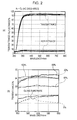
- Fig. 2 shows transmittance and reflectance curves in the case of the AC discharge (in which the O 2 flow rate ratio was 0%, 20%, 40%, 50%, or 100%). All the samples showed substantially constant transmittance and reflectance in a wavelength range of 400 nm or more ((a) of Fig. 2 ). Furthermore, the samples prepared at an O 2 flow rate ratio of 20%, 40%, 50%, and 100% showed higher transmittances than that of a glass substrate ((b) of Fig. 2 ).
- sputtering deposition was performed under the deposition conditions below using a radio-frequency power supply (RF power supply) instead of the AC power supply 2 in the reactive sputtering apparatus SE shown in Fig. 1 .
- RF power supply radio-frequency power supply
- an antireflection film having the structure shown in Fig. 4 was prepared in the order described below on the basis of the respective deposition conditions below.
- Fig. 5 shows a measurement result of a spectral reflectance characteristic of the obtained antireflection film sample.
- a blackening treatment was performed on the reverse face of the sample in order to remove reflection components.
Landscapes
- Chemical & Material Sciences (AREA)
- Metallurgy (AREA)
- Physics & Mathematics (AREA)
- Chemical Kinetics & Catalysis (AREA)
- Engineering & Computer Science (AREA)
- Materials Engineering (AREA)
- Mechanical Engineering (AREA)
- Organic Chemistry (AREA)
- General Physics & Mathematics (AREA)
- Optics & Photonics (AREA)
- Inorganic Chemistry (AREA)
- Physical Vapour Deposition (AREA)
- Surface Treatment Of Optical Elements (AREA)
Abstract
Provided is a method of depositing a low-refractive-index film, by which a thin film having uniform composition distribution in the film and having a low refractive index can be formed, a low-refractive-index film deposited by the method of depositing a low-refractive-index film, and furthermore, an antireflection film including the low-refractive-index film. In a method of depositing a low-refractive-index film including depositing a low-refractive-index film composed of MgF2-SiO2 on a substrate 11 by a reactive sputtering method, sputtering deposition is conducted using targets 4A and 4B composed of a sintered body of MgF2-SiO2 by applying an alternating voltage with a frequency in the range of 20 to 90 kHz between the substrate 11 and the targets 4A and 4B in an atmosphere of a mixed gas of an inert gas and O2.
Description
- The present invention relates to a low-refractive-index film deposited by a reactive sputtering method, a method of depositing the same, and an antireflection film including the low-refractive-index film.
- In general, in a display device such as a cathode ray tube (CRT) or a liquid crystal display, an antireflection film is provided on a surface on which an image is displayed. This antireflection film is provided in order to reduce reflection of external light to reproduce a preferred image or text information and formed by stacking thin-film materials having different refractive indices.
- Such an antireflection film is constituted by stacking, for example, on a transparent film base composed of an organic material, a low-refractive-index layer composed of a low-refractive-index material such as silicon oxide, silicon nitride, or magnesium fluoride and a high-refractive-index layer composed of a high-refractive-index material such as tin oxide-containing indium oxide (ITO), titanium oxide, tantalum oxide, or zirconium oxide.
- Here, as for the low-refractive-index material, Japanese Unexamined Patent Application Publication No.
4-223401 - Furthermore, Japanese Unexamined Patent Application Publication No.
2004-315834 - In order to solve the above problems, a MgF2-SiO2 target should be prepared by mixing stable materials, such as MgF2 and SiO2, with each other. However, even when such a target is used, it is difficult to deposit a low-refractive-index film suitable for an antireflection film.
- The present invention has been made in view of the above problems in the related art. It is an object of the present invention to provide a method of depositing a low-refractive-index film, by which a thin film having a uniform composition distribution in the film and having a low refractive index can be formed, and a low-refractive-index film deposited by the method of depositing a low-refractive-index film. Furthermore, it is an object of the present invention to provide an antireflection film including the low-refractive-index film.
- The present invention provided in order to solve the above problems is a method of depositing a low-refractive-index film including depositing a low-refractive-index film composed of MgF2-SiO2 on a substrate by a reactive sputtering method, characterized in that sputtering deposition is conducted using a target composed of a sintered body of MgF2-SiO2 by applying an alternating voltage with a frequency in the range of 20 to 90 kHz between the substrate and the target in an atmosphere of a mixed gas of Ar and O2.
- Here, the content of SiO2 in the target is preferably in the range of 5 to 80 mole percent.
- Furthermore, an O2 flow rate ratio of the mixed gas is preferably in the range of 10% to 70%.
- In addition, the present invention provided in order to solve the above problems is a low-refractive-index film characterized by being deposited by the method of depositing a low-refractive-index film described in any one of
Claims 1 to 3. - In addition, the present invention provided in order to solve the above problems is an antireflection film characterized in that a high-refractive-index layer and a low-refractive-index layer composed of the low-refractive-index film described in Claim 4 are stacked on a substrate.
- According to the method of depositing a low-refractive-index film of the present invention, a low-refractive-index film composed of a fluoride and having a uniform composition distribution can be deposited by a sputtering method. In addition, by appropriately adjusting the composition of MgF2-SiO2, a low-refractive-index film having any optical properties can be obtained.
- According to the low-refractive-index film of the present invention, a low-refractive-index film having uniform optical properties in the film surface can be provided.
- According to the low-refractive-index film of the present invention, an antireflection film having a uniform and good antireflection function in the film surface can be provided.
-
- [
Fig. 1] Fig. 1 is a schematic view showing the structure of a reactive sputtering apparatus used in the present invention. - [
Fig. 2] Fig. 2 includes transmittance and reflectance curves of samples prepared in Example 1 under the conditions of an introduced mixed gas of Ar + O2 and an AC discharge. - [
Fig. 3] Fig. 3 includes transmittance and reflectance curves of samples prepared in Example 1 under the conditions of an introduced mixed gas of Ar + CF4. - [
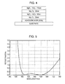
Fig. 4] Fig. 4 is a cross-sectional view showing the structure of an antireflection film of Example 2. - [
Fig. 5] Fig. 5 is a graph showing a spectral reflectance characteristic of the antireflection film of Example 2. - A method of depositing a low-refractive-index film according to the present invention will be described below. Note that the present invention will be described on the basis of embodiments shown in the drawings, but the present invention is not limited thereto and can be appropriately changed in accordance with an embodiment. Any embodiment is included within the scope of the present invention as long as operations and advantages of the present invention can be achieved.
- The method of depositing a low-refractive-index film according to the present invention is a method of depositing a low-refractive-index film including depositing a low-refractive-index film composed of MgF2-SiO2 on a substrate by a reactive sputtering method, characterized in that sputtering deposition is conducted using a target composed of a sintered body of MgF2-SiO2 by applying an alternating voltage with a frequency in the range of 20 to 90 kHz between the substrate and the target in an atmosphere of a mixed gas of Ar and O2.
- Here,
Fig. 1 shows a structural example of a reactive sputtering apparatus to which the method of depositing a low-refractive-index film of the present invention is applied. - As shown in
Fig. 1 , a reactive sputtering apparatus SE includes avacuum chamber 1, asubstrate holder 5 that holds asubstrate 11 on which a thin film is to be formed, thesubstrate holder 5 being disposed on an upper part of the inside of thevacuum chamber 1, and driving means 6 for rotating thesubstrate holder 5. Furthermore, a vacuum pump (not shown) for evacuating the inside of thevacuum chamber 1 is connected to thevacuum chamber 1, and thus thevacuum chamber 1 is configured so that the degree of vacuum in the inside of thevacuum chamber 1 can be adjusted to any value. - On the lower part of the inside of the
vacuum chamber 1, sputtering electrodes (cathodes) 3A and 3B, which are connected to anAC power supply 2 serving as a sputtering power supply, and targets 4A and 4B having a flat-plate shape and disposed on the sputteringelectrodes substrate 11. Note that thetargets - In addition, two types of gas introduction pipes 7 for introducing gases into the chamber are connected to the
vacuum chamber 1. One of the pipes is configured so that a sputtering gas, the flow rate of which is adjusted by a mass flow controller which is not shown in the figure, is introduced into thevacuum chamber 1. Here, the sputtering gas is an inert gas, and is preferably, for example, one or more types of gases selected from Ar, Xe, Ne, and Kr. - Furthermore, the other pipe is configured so that O2 gas, the flow rate of which is adjusted by a mass flow controller which is not shown in the figure, is introduced as a reactive gas into the
vacuum chamber 1. - Accordingly, the atmosphere in the
vacuum chamber 1 becomes a mixed atmosphere of the inert gas and O2 gas, and thetargets - Note that in the present invention, various known sputtering methods such as magnetron sputtering, diode sputtering in which magnetron discharge is not used, ECR sputtering, and bias sputtering can be used.
- Here, a low-refractive-index film of the present invention is obtained by performing deposition by the following procedure using the reactive sputtering apparatus SE.
(S11) Thesubstrate 11 is held on thesubstrate holder 5, and thetargets electrodes
(S12) The inside of thevacuum chamber 1 is evacuated so that the pressured in the inside thereof is reduced to a predetermined pressure or less, and thesubstrate holder 5 is rotated.
(S13) The sputtering gas and O2 gas are introduced into thevacuum chamber 1. In this step, the O2 gas and the sputtering gas are introduced while adjusting the flow rates of the gases to a predetermined flow rate ratio, thus controlling to the predetermined pressure. The O2 flow rate ratio is preferably, for example, in the range of 10% to 70%, and most preferably in the range of 20% to 50%.
(S14) Next, an electrical power is provided to the sputteringelectrodes targets targets
(S15) When a sputtering state becomes stable, deposition on thesubstrate 11 attached to thesubstrate holder 5 is started. Thus, a low-refractive-index film composed of MgF2-SiO2 having a predetermined thickness is obtained. - A transparent thin film composed of MgF2-SiO2 and having a lower refractive index than that of a SiO2 film can be readily formed by this deposition method.
- Examples performed for verifying the present invention will be described below.
- A description will be made of an example in which low-refractive-index films were deposited by the method of depositing a low-refractive-index film of the present invention using the reactive sputtering apparatus SE shown in
Fig. 1 . Note that, as for sputtering conditions, targets 4A and 4B: MgF2-SiO2 sintered body (MgF2:SiO2 = 70:30 atomic percent), sputtering gas: Ar, and reactive gas: O2 were used as common conditions, and the Ar gas was introduced with a back pressure in thevacuum chamber 1 of 5 × 10⁻⁴ Pa or less, and pre-sputtering was performed. Subsequently, low-refractive-index films were prepared under the deposition conditions below. Note that (O2 gas flow rate ratio) = (O2 gas flow rate)/{(O2 gas flow rate) + (Ar gas flow rate)} × 100 (%). -
- · Substrate 11: transparent glass substrate
- · O2 gas flow rate ratio: 0%, 20%, 40%, 50%, and 100%
- · Frequency of AC power supply: 90 kHz
- · Supplied electrical power: 400 W
- · Total pressure: 0.37 to 0.39 Pa
- Furthermore, sputtering deposition was performed under the deposition conditions below using a radio-frequency power supply (RF power supply) instead of the
AC power supply 2 in the reactive sputtering apparatus SE shown inFig. 1 . -
- · Substrate 11: transparent glass substrate
- ·
Targets - · O2 gas flow rate ratio: 0%, 20%, and 50%
- · Frequency of RF power supply: 13.56 MHz
- · Supplied electrical power: 300 W
- · Total pressure: 0.39 Pa
- The refractive indices and extinction coefficients at a wavelength of 550 nm, and the transmittances of the obtained samples were measured. The results are shown in Table 1. In the case of AC discharge (in the case where the AC power supply was used), the refractive index and extinction coefficient of the sample prepared at an O2 flow rate ratio of O% could not be measured because of high absorption, but the refractive indices of other samples (prepared at an O2 flow rate ratio of 20%, 40%, 50%, and 100%) were less than 1.5 (about 1.4). Furthermore, according to the results of an XPS analysis of the composition of the optical film of Sample No. 4 (Ar: 100 sccm, O2: 100 sccm, O2 flow rate ratio: 50%, total pressure: 0.38 Pa, and electrical power: 400 W), C was 3.89 atomic percent, O was 9.99 atomic percent, F was 55.53 atomic percent, Mg was 27.92 atomic percent, Si was 2.66 atomic percent, and the concentration ratio of F to Mg was 1.99. In addition, in the case of RF discharge (in the case where the radio-frequency power supply was used), the refractive indices were 1.5 or more, and thus it is believed that optical films composed of MgO and SiO2 were formed.
[Table 1] No. Discharge method Introduced gas Total pressure (Pa) Electrical power (W) Film thickness (nm) Deposition rate (nm/min) Evaluation results Ar (sccm) O2 (sccm) O2 flow rate ratio Refractive index (550 nm) Extinction coefficient k (550 nm) Transmittance*1 (%) 1 AC 200 0 0% 0.39 400 40 0.36 Could not be measured. Could not be measured. 91.67 2 AC 160 40 20% 0.39 400 80.9 0.34 1.406 0 94.09 3 AC 120 80 40% 0.39 400 72.1 0.33 1.445 0 93.08 4 AC 100 100 50% 0.38 400 89.6 0.37 1.390 0 94.28 5 AC 0 200 100% 0.37 400 85.8 0.36 1.464 0 94.17 6 RF 200 0 0% 0.39 300 178.3 1.49 1.544 0.003792 87.96 7 RF 160 40 20% 0.39 300 163.4 1.36 1.563 0 92.24 8 RF 100 100 50% 0.39 300 131.6 1.10 Could not be measured. Could not be measured. 91.40 *Average of the transmittances at wavelengths in the range of 500 to 600 nm. -
Fig. 2 shows transmittance and reflectance curves in the case of the AC discharge (in which the O2 flow rate ratio was 0%, 20%, 40%, 50%, or 100%). All the samples showed substantially constant transmittance and reflectance in a wavelength range of 400 nm or more ((a) ofFig. 2 ). Furthermore, the samples prepared at an O2 flow rate ratio of 20%, 40%, 50%, and 100% showed higher transmittances than that of a glass substrate ((b) ofFig. 2 ). - Next, thin-film samples were prepared under the conditions below using the reactive sputtering apparatus SE shown in
Fig. 1 . -
- · Substrate 11: transparent glass substrate
- ·
Targets - · Introduced mixed gas: Ar + CF4
- · Gas flow rate (Ar/CF4): 160/40, 100/100, and 0/200 sccm (20%, 50%, and 100%, respectively, in terms of the CF4 gas flow rate ratio)
- · Frequency of AC power supply: 90 kHz
- · Supplied electrical power: 400 W
- · Total pressure: 0.4 to 0.43 Pa
-
- · Substrate 11: transparent glass substrate
- ·
Targets - · Introduced mixed gas: Ar + O2 + CF4
- · Gas flow rate (Ar/O2/CF4) : 100/10/90, 100/30/70, and 100/70/30 sccm
- · Frequency of AC power supply: 90 kHz
- · Supplied electrical power: 400 W
- · Total pressure: 0.4 Pa
-
- ·
Targets - · Introduced mixed gas: Ar + CO2
- · Gas flow rate (Ar/CO2): 160/40, 100/100, and 0/200 sccm (20%, 50%, and 100%, respectively, in terms of the CO2 gas flow rate ratio)
- · Frequency of AC power supply: 90 kHz
- · Supplied electrical power: 400 W
- · Total pressure: 0.38 to 0.39 Pa
- Furthermore, sputtering deposition was performed under the deposition conditions below using a radio-frequency power supply (RF power supply) instead of the
AC power supply 2 in the reactive sputtering apparatus SE shown inFig. 1 . -
- ·
Targets - · Introduced mixed gas: Ar + CF4
- · Gas flow rate (Ar/CF4): 100/100 and 0/200 sccm (50% and 100%, respectively, in terms of the CF4 gas flow rate ratio)
- · Frequency of RF power supply: 13.56 MHz
- · Supplied electrical power: 300 W
- · Total pressure: 0.42 to 0.45 Pa
- The refractive indices and extinction coefficients at a wavelength of 550 nm, and the transmittances of the obtained samples were measured. The results are shown in Table 2.
[Table 2] No. Discharge method Introduced gas Total pressure (Pa) Electrical power (W) Film thickness (nm) Deposition rate (nm/min) Evaluation results Ar (sccm) O2 (sccm) CF4 (sccm) CO2 (sccm) Refractive index (550 nm) Extinction coefficient k (550 nm) Transmittance*1 (%) 9 AC 160 0 40 0 0.4 400 79 0.44 Could not be measured. Could not be measured. 89.44 10 AC 100 0 100 0 0.41 400 77 0.43 Could not be measured. Could not be measured. 87.96 11 AC 0 0 200 0 0.43 400 88 0.49 Could not be measured. Could not be measured. 88.27 12 AC 100 10 90 0 0.4 400 86.8 0.41 Could not be measured. Could not be measured. 84.39 13 AC 100 30 70 0 0.4 400 64 0.30 Could not be measured. Could not be measured. 84.93 14 AC 100 70 30 0 0.4 400 65.2 0.31 Could not be measured. Could not be measured. 89.74 15 AC 160 0 0 40 0.39 400 74.4 0.31 1.598 0.004195 91.45 16 AC 100 0 0 100 0.38 400 91.1 0.38 1.607 0 90.30 17 AC 0 0 0 200 0.38 400 92.6 0.39 1.448 0 92.19 18 RF 100 0 100 0 0.42 300 221 1.84 Could not be measured. Could not be measured. 69.49 19 RF 0 0 200 0 0.45 300 241.8 2.02 Could not be measured. Could not be measured. 80.55 *Average of the transmittances at wavelengths in the range of 500 to 600 nm. - In all the samples obtained in the case where CF4 gas was introduced, namely, Sample Nos. 9 to 11 (introduced mixed gas: Ar + CF4, AC-discharge samples), Sample Nos. 12 to 14 (introduced mixed gas: Ar + O2 + CF4, AC-discharge samples), and Sample Nos. 18 and 19 (introduced mixed gas: Ar + CF4, RF-discharge samples), since absorption was large, the refractive index and the extinction coefficient could not be measured. Furthermore,
Fig. 3 shows transmittance and reflectance curves of the samples prepared using an introduced mixed gas of Ar + CF4. As compared with the transmittance and reflectance curves of the samples prepared using an introduced mixed gas of Ar + O2, which is shown inFig. 2 , it was found that, in the AC discharge ((a) ofFig. 3 ), films that absorbed light at the short-wavelength side were obtained. In addition, in the RF discharge ((b) ofFig. 3 ), films that further absorbed light were obtained. Note that, in Table 2, the refractive indices of the samples prepared using an introduced mixed gas of Ar + CO2 (Sample Nos. 15 and 16) were high; about 1.6. - According to the above results, it is believed that, in order to prepare a thin film that has a lower refractive index than that of SiO2 and that does not have absorption in the visible light range using a MgF2-SiO2 (70:30 atomic percent) target, it is necessary to deposit in an Ar + O2 atmosphere using AC discharge. It is believed that an appropriate O2 flow rate ratio in this case is in the range of 10% to 70%.
- A description will be made of an example of a deposition of an antireflection film using the reactive sputtering apparatus SE shown in
Fig. 1 . - Here, an antireflection film having the structure shown in
Fig. 4 was prepared in the order described below on the basis of the respective deposition conditions below. - (1) Substrate: Glass substrate
- (2) Adhesion layer: SiOx
- · Sputtering target: B-doped polycrystalline Si
- · Sputtering gas: Ar
- · Reactive gas: O2
- (3) High-refractive-index layer a: Nb2O5
- · Sputtering target: Metal Nb
- · Sputtering gas: Ar
- · Reactive gas: CO2
- · Film thickness: 25 nm
- (4) Low-refractive-index layer a: MgF2-SiO2
- · Sputtering
targets - · Sputtering gas: Ar
- · Reactive gas: O2
- · Deposition conditions: The same as those used in Sample No. 4 in Example 1
- · Film thickness: 40 nm
- · Sputtering
- (5) High-refractive-index layer b: Nb2O5
- · Sputtering target: Metal Nb
- · Sputtering gas: Ar
- · Reactive gas: CO2
- · Film thickness: 30 nm
- (6) Low-refractive-index layer b: MgF2-SiO2
- · Sputtering
targets - · Sputtering gas: Ar
- · Reactive gas: O2
- · Deposition conditions: The same as those used in Sample No. 4 in Example 1
- · Film thickness: 115 nm
- · Sputtering
-
Fig. 5 shows a measurement result of a spectral reflectance characteristic of the obtained antireflection film sample. In the measurement of the reflectance, a blackening treatment was performed on the reverse face of the sample in order to remove reflection components.
Claims (5)
- A method of depositing a low-refractive-index film comprising depositing a low-refractive-index film composed of MgF2-SiO2 on a substrate by a reactive sputtering method,
characterized in that sputtering deposition is conducted using a target composed of a sintered body of MgF2-SiO2 by applying an alternating voltage with a frequency in the range of 20 to 90 kHz between the substrate and the target in an atmosphere of a mixed gas of an inert gas and O2. - The method of depositing a low-refractive-index film according to Claim 1, characterized in that the content of SiO2 in the target is in the range of 5 to 80 mole percent.
- The method of depositing a low-refractive-index film according to Claim 1, characterized in that an O2 flow rate ratio of the mixed gas is in the range of 10% to 70%.
- A low-refractive-index film characterized by being deposited by the method of depositing a low-refractive-index film according to any one of Claims 1 to 3.
- An antireflection film characterized in that a high-refractive-index layer and a low-refractive-index layer composed of the low-refractive-index film according to Claim 4 are stacked on a substrate.
Applications Claiming Priority (2)
| Application Number | Priority Date | Filing Date | Title |
|---|---|---|---|
| JP2007170584A JP2009007636A (en) | 2007-06-28 | 2007-06-28 | Low refractive index film, film forming method thereof, and antireflection film |
| PCT/JP2008/059189 WO2009001634A1 (en) | 2007-06-28 | 2008-05-20 | Low-refractive index film, method for forming the low-refractive index film, and antireflection film |
Publications (1)
| Publication Number | Publication Date |
|---|---|
| EP2159301A1 true EP2159301A1 (en) | 2010-03-03 |
Family
ID=40185457
Family Applications (1)
| Application Number | Title | Priority Date | Filing Date |
|---|---|---|---|
| EP08752985A Withdrawn EP2159301A1 (en) | 2007-06-28 | 2008-05-20 | Low-refractive index film, method for forming the low-refractive index film, and antireflection film |
Country Status (6)
| Country | Link |
|---|---|
| US (1) | US20100186630A1 (en) |
| EP (1) | EP2159301A1 (en) |
| JP (1) | JP2009007636A (en) |
| KR (1) | KR20100028535A (en) |
| CN (1) | CN101688292B (en) |
| WO (1) | WO2009001634A1 (en) |
Families Citing this family (6)
| Publication number | Priority date | Publication date | Assignee | Title |
|---|---|---|---|---|
| JP5577287B2 (en) * | 2011-03-30 | 2014-08-20 | 日本碍子株式会社 | Magnesium fluoride sintered body, manufacturing method thereof, and member for semiconductor manufacturing apparatus |
| US9746678B2 (en) * | 2014-04-11 | 2017-08-29 | Applied Materials | Light wave separation lattices and methods of forming light wave separation lattices |
| KR101660300B1 (en) | 2014-12-30 | 2016-09-27 | 한국세라믹기술원 | Manufacturing method of low refractive anti-reflection film using ultrasonic spray coating method |
| CN107219567B (en) * | 2017-06-21 | 2019-06-28 | 北京富兴凯永兴光电技术有限公司 | A kind of uniform low-refraction optical filming material and preparation method of forming a film |
| CN114173667B (en) * | 2019-07-26 | 2026-01-27 | 万迈医疗仪器有限公司 | Interferometric sensor for biochemical tests |
| CN116840947A (en) * | 2023-03-01 | 2023-10-03 | 安徽立光电子材料股份有限公司 | Magnetron sputtering infrared antireflection film with wide incident angle and preparation method thereof |
Family Cites Families (20)
| Publication number | Priority date | Publication date | Assignee | Title |
|---|---|---|---|---|
| JPH0642003B2 (en) * | 1983-09-20 | 1994-06-01 | オリンパス光学工業株式会社 | Antireflection film for optical parts and method for forming the same |
| JP3079580B2 (en) * | 1990-12-25 | 2000-08-21 | 株式会社ニコン | Thin film for optical component, optical component having the same, and method of manufacturing the same |
| US5744227A (en) * | 1995-04-03 | 1998-04-28 | Southwall Technologies Inc. | Antireflective coatings comprising a lubricating layer having a specific surface energy |
| WO1996034124A1 (en) * | 1995-04-25 | 1996-10-31 | The Boc Group, Inc. | Sputtering system using cylindrical rotating magnetron electrically powered using alternating current |
| JP3808917B2 (en) * | 1995-07-20 | 2006-08-16 | オリンパス株式会社 | Thin film manufacturing method and thin film |
| JPH09249968A (en) * | 1996-03-14 | 1997-09-22 | Olympus Optical Co Ltd | Production of optical thin film and device therefor |
| DE19644752A1 (en) * | 1996-10-28 | 1998-04-30 | Leybold Systems Gmbh | Interference layer system |
| JP3190610B2 (en) * | 1996-12-04 | 2001-07-23 | ティアールダブリュー インコーポレイテッド | Method for forming a substantially flat film |
| JPH10195636A (en) * | 1996-12-26 | 1998-07-28 | Oike Ind Co Ltd | Antireflection material excellent in durability |
| US6266193B1 (en) * | 1997-07-24 | 2001-07-24 | Cpfilms Inc. | Anti-reflective composite |
| TW442672B (en) * | 1999-11-25 | 2001-06-23 | Nat Science Council | The technique for deposition multilayer interference thin films by using only one coating material (pure silicon) |
| CN1258616C (en) * | 2001-02-07 | 2006-06-07 | 旭硝子株式会社 | Sputtering device and sputtering film forming method |
| JP4033286B2 (en) * | 2001-03-19 | 2008-01-16 | 日本板硝子株式会社 | High refractive index dielectric film and manufacturing method thereof |
| KR20030013428A (en) * | 2001-03-22 | 2003-02-14 | 소니 가부시끼 가이샤 | Reflective display device, light guide plate, and method of manufacturing light guide plate |
| US20030201164A1 (en) * | 2002-04-29 | 2003-10-30 | Johnson Linda F. | Method of making electrically conductive, IR transparent metal oxide films |
| JP4442178B2 (en) * | 2002-10-07 | 2010-03-31 | Tdk株式会社 | Hologram recording medium |
| JP4486838B2 (en) * | 2003-04-25 | 2010-06-23 | 旭硝子株式会社 | Method for producing silicon oxide film and method for producing optical multilayer film |
| JP2005048260A (en) * | 2003-07-31 | 2005-02-24 | Canon Inc | Reactive sputtering method |
| US20080316628A1 (en) * | 2007-06-25 | 2008-12-25 | Nisca Corporation | Density filter, method of forming the density filter and apparatus thereof |
| JP4492691B2 (en) * | 2007-12-14 | 2010-06-30 | ソニー株式会社 | Method for forming transparent optical film |
-
2007
- 2007-06-28 JP JP2007170584A patent/JP2009007636A/en not_active Ceased
-
2008
- 2008-05-20 US US12/666,453 patent/US20100186630A1/en not_active Abandoned
- 2008-05-20 KR KR1020097023555A patent/KR20100028535A/en not_active Withdrawn
- 2008-05-20 EP EP08752985A patent/EP2159301A1/en not_active Withdrawn
- 2008-05-20 CN CN2008800219990A patent/CN101688292B/en not_active Expired - Fee Related
- 2008-05-20 WO PCT/JP2008/059189 patent/WO2009001634A1/en not_active Ceased
Non-Patent Citations (1)
| Title |
|---|
| See references of WO2009001634A1 * |
Also Published As
| Publication number | Publication date |
|---|---|
| US20100186630A1 (en) | 2010-07-29 |
| CN101688292B (en) | 2012-03-21 |
| WO2009001634A1 (en) | 2008-12-31 |
| CN101688292A (en) | 2010-03-31 |
| JP2009007636A (en) | 2009-01-15 |
| KR20100028535A (en) | 2010-03-12 |
Similar Documents
| Publication | Publication Date | Title |
|---|---|---|
| JP3808917B2 (en) | Thin film manufacturing method and thin film | |
| JP4147743B2 (en) | Light-absorbing antireflection body and method for producing the same | |
| JP2000356706A (en) | Light-absorbing antireflective body and method for producing the same | |
| US20110194181A1 (en) | Film forming method for antireflection film, antireflection film, and film forming device | |
| EP2159301A1 (en) | Low-refractive index film, method for forming the low-refractive index film, and antireflection film | |
| US20010016262A1 (en) | Method of coating substrate and coated article | |
| US6217719B1 (en) | Process for thin film formation by sputtering | |
| GB2372044A (en) | Functional film with concentration gradient | |
| CN104090312A (en) | Infrared metal reflecting film with high adhesive force and manufacturing method thereof | |
| US7842168B2 (en) | Method for producing silicon oxide film and method for producing optical multilayer film | |
| JP6392912B2 (en) | Deposition method | |
| JP6995491B2 (en) | Manufacturing method of optical thin film, optical element, optical element | |
| WO1991002102A1 (en) | Film based on silicon dioxide and production thereof | |
| JP3190240B2 (en) | Light-absorbing antireflective body and method for producing the same | |
| JP7418098B2 (en) | Method for forming optical multilayer film and method for manufacturing optical element | |
| US20030027001A1 (en) | Anti-reflective and anti-static multi-layer thin film for display device | |
| US20090152102A1 (en) | Transparent optical film and method of forming the same | |
| US20040157044A1 (en) | Anti-reflective and anti-static multi-layer thin film for display device | |
| EP1184879A1 (en) | Conductive nitride film, process for producing the same, and antireflection object | |
| JP6366263B2 (en) | Optical multilayer film, optical lens, and method of manufacturing optical multilayer film | |
| JP2002071902A (en) | Light absorbing anti-reflective body | |
| JP5123785B2 (en) | Method for forming antireflection film and antireflection film | |
| JP2007154242A (en) | Manufacturing method of mixed oxide film | |
| JP4793056B2 (en) | Sputter deposition method of antireflection film | |
| JP2697000B2 (en) | Article coated with optical film |
Legal Events
| Date | Code | Title | Description |
|---|---|---|---|
| PUAI | Public reference made under article 153(3) epc to a published international application that has entered the european phase |
Free format text: ORIGINAL CODE: 0009012 |
|
| 17P | Request for examination filed |
Effective date: 20091210 |
|
| AK | Designated contracting states |
Kind code of ref document: A1 Designated state(s): AT BE BG CH CY CZ DE DK EE ES FI FR GB GR HR HU IE IS IT LI LT LU LV MC MT NL NO PL PT RO SE SI SK TR |
|
| AX | Request for extension of the european patent |
Extension state: AL BA MK RS |
|
| DAX | Request for extension of the european patent (deleted) | ||
| STAA | Information on the status of an ep patent application or granted ep patent |
Free format text: STATUS: THE APPLICATION HAS BEEN WITHDRAWN |
|
| 18W | Application withdrawn |
Effective date: 20120323 |