EP2157705A2 - Wireless communication device and power receiving device - Google Patents
Wireless communication device and power receiving device Download PDFInfo
- Publication number
- EP2157705A2 EP2157705A2 EP09167699A EP09167699A EP2157705A2 EP 2157705 A2 EP2157705 A2 EP 2157705A2 EP 09167699 A EP09167699 A EP 09167699A EP 09167699 A EP09167699 A EP 09167699A EP 2157705 A2 EP2157705 A2 EP 2157705A2
- Authority
- EP
- European Patent Office
- Prior art keywords
- communication
- unit
- antenna
- power
- processing unit
- Prior art date
- Legal status (The legal status is an assumption and is not a legal conclusion. Google has not performed a legal analysis and makes no representation as to the accuracy of the status listed.)
- Granted
Links
- 238000004891 communication Methods 0.000 title claims abstract description 410
- 238000012545 processing Methods 0.000 claims abstract description 219
- 238000010248 power generation Methods 0.000 claims abstract description 46
- 230000005674 electromagnetic induction Effects 0.000 claims abstract description 21
- 230000005540 biological transmission Effects 0.000 description 59
- 239000003999 initiator Substances 0.000 description 6
- 230000004044 response Effects 0.000 description 6
- 230000006870 function Effects 0.000 description 5
- 239000003990 capacitor Substances 0.000 description 4
- 238000010586 diagram Methods 0.000 description 4
- 238000006243 chemical reaction Methods 0.000 description 3
- 238000009499 grossing Methods 0.000 description 3
- 230000007246 mechanism Effects 0.000 description 3
- 238000012546 transfer Methods 0.000 description 3
- 230000004075 alteration Effects 0.000 description 2
- 230000008878 coupling Effects 0.000 description 2
- 238000010168 coupling process Methods 0.000 description 2
- 238000005859 coupling reaction Methods 0.000 description 2
- 238000012986 modification Methods 0.000 description 2
- 230000004048 modification Effects 0.000 description 2
- 230000008859 change Effects 0.000 description 1
- 238000013461 design Methods 0.000 description 1
- 238000001514 detection method Methods 0.000 description 1
- 230000010354 integration Effects 0.000 description 1
- 239000004973 liquid crystal related substance Substances 0.000 description 1
- 230000005855 radiation Effects 0.000 description 1
Images


Classifications
-
- H—ELECTRICITY
- H04—ELECTRIC COMMUNICATION TECHNIQUE
- H04B—TRANSMISSION
- H04B5/00—Near-field transmission systems, e.g. inductive or capacitive transmission systems
- H04B5/40—Near-field transmission systems, e.g. inductive or capacitive transmission systems characterised by components specially adapted for near-field transmission
- H04B5/48—Transceivers
-
- G—PHYSICS
- G06—COMPUTING; CALCULATING OR COUNTING
- G06K—GRAPHICAL DATA READING; PRESENTATION OF DATA; RECORD CARRIERS; HANDLING RECORD CARRIERS
- G06K7/00—Methods or arrangements for sensing record carriers, e.g. for reading patterns
- G06K7/0008—General problems related to the reading of electronic memory record carriers, independent of its reading method, e.g. power transfer
-
- H—ELECTRICITY
- H01—ELECTRIC ELEMENTS
- H01Q—ANTENNAS, i.e. RADIO AERIALS
- H01Q1/00—Details of, or arrangements associated with, antennas
- H01Q1/12—Supports; Mounting means
- H01Q1/22—Supports; Mounting means by structural association with other equipment or articles
- H01Q1/2208—Supports; Mounting means by structural association with other equipment or articles associated with components used in interrogation type services, i.e. in systems for information exchange between an interrogator/reader and a tag/transponder, e.g. in Radio Frequency Identification [RFID] systems
-
- H—ELECTRICITY
- H02—GENERATION; CONVERSION OR DISTRIBUTION OF ELECTRIC POWER
- H02J—CIRCUIT ARRANGEMENTS OR SYSTEMS FOR SUPPLYING OR DISTRIBUTING ELECTRIC POWER; SYSTEMS FOR STORING ELECTRIC ENERGY
- H02J50/00—Circuit arrangements or systems for wireless supply or distribution of electric power
- H02J50/10—Circuit arrangements or systems for wireless supply or distribution of electric power using inductive coupling
- H02J50/12—Circuit arrangements or systems for wireless supply or distribution of electric power using inductive coupling of the resonant type
-
- H—ELECTRICITY
- H02—GENERATION; CONVERSION OR DISTRIBUTION OF ELECTRIC POWER
- H02J—CIRCUIT ARRANGEMENTS OR SYSTEMS FOR SUPPLYING OR DISTRIBUTING ELECTRIC POWER; SYSTEMS FOR STORING ELECTRIC ENERGY
- H02J7/00—Circuit arrangements for charging or depolarising batteries or for supplying loads from batteries
- H02J7/0068—Battery or charger load switching, e.g. concurrent charging and load supply
Definitions
- the invention relates to a wireless communication device and a power receiving device.
- the invention relates to the wireless communication device and the power receiving device capable of performing communication and the like while obtaining sufficient power even when communication is performed in a state in which antennas of transmission-side and receiving-side wireless communication devices make contact with each other closely.
- an NFCIP-1 Near Field Communication Interface and Protocol-1
- a reader/writer and an IC card complying with the NFCIP-1 standard are broadly used for individual authentication, electronic money payment and the like.
- NFCIP-1 type In data communication using a type complying with the NFCIP-1 standard (hereinafter, referred to as an "NFCIP-1 type"), a passive communication mode and an active communication mode by 13.56MHz electromagnetic induction coupling are prescribed.
- a passive communication mode a non-modulated carrier signal is transmitted from the reader/writer to the IC card.
- the IC card modulates the transmitted non-modulated carrier signal in accordance with data to be transmitted.
- the reader/writer obtains data transmitted from the IC card by performing demodulation and the like of the modulated carrier signal. Accordingly, in the passive communication mode, communication is performed without generation of the carrier signal by the IC card itself. Also in the passive communication mode, power generation is performed by using the carrier signal transmitted from the reader/writer and operations of the IC card are performed by using the generated power.
- the IC card itself generates the carrier signal, modulates the generated carrier signal in accordance with data to be transmitted, then, transmits the signal.
- the reader/writer performs demodulation and the like of the modulated carrier signal, thereby obtaining data transmitted from the IC card.
- processing of generating the carrier signal, modulating the generated carrier signal in accordance with data to be transmitted and transmitting the modulated carrier signal is performed by providing a power supply unit using a primary battery or a secondary battery in the IC card and supplying power to respective units of the IC card from the power supply unit.
- the IC card In the case of the passive communication mode, it is assumed that main applications of the IC card used for the near-field wireless communication are individual authentication (for example, at an entrance gate), electronic money payment (for example, at a vending machine" and the like, therefore, the IC card is designed so that communication stability can be obtained maximally when the IC card is carried by a human hand, for example, when the reader/writer and the IC card is several centimeters apart from each other. Accordingly, it is difficult to obtain stable power in conditions different from the case in which the card is operated by a human hand. For example, when communication of video contents or audio contents is performed by using the reader/writer and the IC card, the IC card is placed on the reader/writer in a state of touching the reader/writer, therefore, it is difficult to obtain stable power.
- a wireless communication device including a first communication processing unit performing communication in an electromagnetic induction system by using a first antenna unit, a second communication processing unit performing communication at higher speed than the first communication processing unit by a system or a communication frequency different from the electromagnetic induction system by using a second antenna unit, and a power generation unit generating power at least for performing communication operations from a carrier signal received by the first antenna unit, in which the power is generated in the power generation unit by switching a frequency resonance characteristic of the first antenna unit.
- communication in the electromagnetic induction system for example, an NFCIP-1 type communication is performed in the first communication processing unit by using the first antenna unit.
- communication higher than the first communication processing unit is performed in the second communication processing unit in a system different from the electromagnetic induction system, for example, a back scatter system by using the second antenna unit.
- power at least for performing communication operations is generated in the power generation unit from the carrier signal received in the first antenna unit.
- the first antenna unit is used in close contact state with the transmission-source antenna unit which transmits the carrier signal.
- the first communication processing unit allows the frequency resonance characteristic of the first antenna unit, for example, a quality factor in an antenna resonant circuit to be high when data communication is performed as well as allows the quality factor to be lower than the time of performing data communication when data communication is not performed, accordingly, power is generated in the power generation unit.
- a content playback unit performing playback of contents is provided, in which the power generation unit supplies generated power to the content playback unit.
- a power supply unit which can be charged is provided, in which the power generation unit charges the power supply unit by using generated power to supply power at least for performing communication operations from the power supply unit.
- a power receiving device including a power generation unit generating power from a carrier signal received by an antenna unit for performing data communication in an electromagnetic induction system, in which power is generated in the power generation unit by switching a frequency resonance characteristic of the antenna unit in accordance with data communication operation in the electromagnetic induction system.
- power is generated in the power generation unit from the carrier signal received by the antenna unit for performing communication in the electromagnetic induction system, for example, the NFCIP-1 type communication.
- the frequency resonance characteristic in the antenna portion for example, the quality factor in the antenna resonant circuit is allowed to be high.
- the quality factor is allowed to be lower than the time of performing data communication.
- the antenna unit is used in a close contact with the transmission-source antenna unit which transmits the carrier signal.
- power is generated in the power generation unit which generates power from the carrier signal received by the antenna unit for performing data communication in the electromagnetic induction system by switching the frequency resonance characteristic of the antenna unit . Accordingly, it is possible to perform near-field wireless communication and the like while obtaining sufficient power even when antennas of transmission-side and receiving-side wireless communication devices are in the close contact state.
- a wireless communication system using a wireless communication device includes, for example, an initiator and a target complying with near-field wireless communication, in which a first antenna unit used for data communication of related art near-field wireless communication, for example, an NFCIP-1 type and a second antenna unit for performing communication at higher speed than near-field wireless communication using the first antenna unit are provided to thereby improving communication speed in the whole system. Further, power is generated from a carrier signal received by the first antenna unit, thereby performing high-speed communication and processing of communication data, charging of a battery and the like by the generated power.
- a first antenna unit used for data communication of related art near-field wireless communication for example, an NFCIP-1 type
- a second antenna unit for performing communication at higher speed than near-field wireless communication using the first antenna unit are provided to thereby improving communication speed in the whole system.
- power is generated from a carrier signal received by the first antenna unit, thereby performing high-speed communication and processing of communication data, charging of a battery and the like by the generated power.
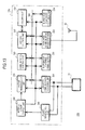
- FIG. 1 shows a configuration of a wireless communication system according to an embodiment of the invention.
- a wireless communication system 10 includes an initiator 20 which starts communication and a target 30 to be a target of the communication.
- the initiator 20 is specifically a reader/writer (R/W) complying with near-field wireless communication operating in a reader/writer mode.
- the reader/writer as the initiator 20 is connected to a host device 40 through a host interface such as a UART (Universal Asynchronous receiver-transmitter).
- the host device 40 corresponds to a personal computer (PC) or an integrated CPU (Central Processing Unit) inside the reader/writer, which performs generation of transmission data, processing of reception data, generation of communication control signals for controlling communication operations and the like.
- PC personal computer
- CPU Central Processing Unit
- the target 30 is a transponder such as the IC card complying with the near-field wireless communication or a reader/writer complying with near-field wireless communication operating in a card mode (hereinafter, these targets are referred to as merely "cards") .
- the card (target) 30 may be a standalone-type or may be connected to a host device 41.
- the reader/writer (initiator 20) is provided with a first antenna unit 21 and a second antenna unit 22.
- the card (target) 30 is provided with a first antenna unit 31 and a second antenna unit 32.
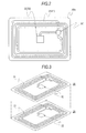
- Fig. 2 shows antenna shapes.
- the card 30 has a shape of, for example, 85.6mm ⁇ 54.0mm which is prescribed by ISO/IEC7816-2, JIS6301-2 standards and the like, the first antenna unit 21 (31) and the second antenna unit 22 (32) are provided within an area ARc of the card size.
- the first antenna unit 21 (31) used for data communication of the related-art near-field wireless communication is formed by a rectangular antenna coil formed along an outer periphery of the card area.
- the second antenna unit 22 (32) used for high-speed communication can perform data communication independently without causing mutual interference with respect to communication using the first antenna unit, which is provided, for example, at the center of the card area ARc so as not to interfere with power supply from the reader/writer 20 to the card 30 by the first antenna unit.
- a control IC chip SC is an integrated circuit of an antenna tuning circuit, a later-described card control unit 33 of the card 30 and the like, to which the first antenna unit and the second antenna unit are connected.
- the first antenna unit 21 is called as a large antenna and a second antenna unit 22 is called as a small antenna.
- the large antenna 21 is connected to a communication processing unit (hereinafter, referred to as a "low-speed communication processing unit) 231 for performing data communication of the related-art near-field wireless communication, for example, the NFCIP-1 type communication.
- the small antenna 22 is connected to a communication processing unit (hereinafter, referred to as a "high-speed communication processing unit) 233 for performing high-speed communication.
- the low-speed communication processing unit 231 of a reader/writer control unit 23 performs coding processing of transmission data read from a buffer for low-speed communication 232, modulation processing of coded data obtained by performing the coding processing and the like so as to perform NFCIP-1 type data communication in the same manner as the related art by using the antenna 21.
- the low-speed communication processing unit 231 generates a transmission signal by performing these processing and supplies the signal to the large antenna 21.
- the low-speed communication processing unit 231 also performs demodulation processing of a reception signal obtained by the large antenna 21, decoding processing of the demodulated signal obtained by performing the demodulation processing and the like.
- the low-speed communication processing unit 231 stores reception data obtained by performing these processing in the buffer for low-speed communication 232.
- Table 1 shows a transfer direction in the NFCIP-1 type, communication speed, a carrier frequency, a modulation scheme, and a coding scheme with respect to respective communication modes.
- the low-speed communication processing unit 231 performs ASK modulation/demodulation processing, Manchester coding/decoding processing and the like.
- the buffer for low-speed communication 232 is a buffer for temporarily storing reception data supplied from the low-speed communication processing unit 231 and transmission data supplied from a communication control unit 243.
- the high-speed communication processing unit 233 performs communication at higher speed than the NFCIP-1 type data communication by using the small antenna 22.
- the high-speed communication processing unit 233 performs coding processing of transmission data read from a buffer for high-speed communication 234, modulation processing of coded data obtained by performing the coding processing and the like.
- the high-speed communication processing unit 233 generates a transmission signal by performing these processing and supplies the signal to the small antenna 22.
- the high-speed communication processing unit 233 also performs demodulation processing of a reception signal obtained by the small antenna 22, decoding processing of the demodulated signal obtained by performing the demodulation processing and the like.
- the high-speed communication processing unit 233 stores reception data obtained by performing these processing in the buffer for high-speed communication 234.
- the high-speed communication processing unit 233 performs a back scatter system, a communication system called as a weak UWB (Ultra Wide Band) using a communication frequency band of 4.48GHz, a baseband broadband communication in the electromagnetic induction system and the like as the communication system which is higher than the NFCIP-1 type data communication.
- a back scatter system a communication system called as a weak UWB (Ultra Wide Band) using a communication frequency band of 4.48GHz, a baseband broadband communication in the electromagnetic induction system and the like as the communication system which is higher than the NFCIP-1 type data communication.
- the high-speed communication processing unit 233 when the back scatter system is used, the high-speed communication processing unit 233 performs ASK modulation/demodulation processing or PSK modulation/demodulation processing, NRZ-L coding/decoding processing and the like.
- the high-speed communication processing unit 233 when transmitting the generated transmission signal, modulates a non-modulated carrier signal supplied from the small antenna 32 of the card 30 in accordance with the transmission signal and reflects the signal.
- the high-speed communication processing unit 233 also generates reception data by receiving the modulated carrier signal supplied from the small antenna 32 of the card 30 and performing demodulation and the like.
- the buffer for high-speed communication 234 is a buffer for temporarily storing reception data supplied from the high-speed communication processing unit 233 and transmission data supplied from the communication control unit 243.
- the communication control unit 243 is connected to the low-speed communication processing unit 231, the buffer for low-speed communication 232, the high-speed communication processing unit 233 and the buffer for high-speed communication 234 through a bus 236.
- the communication control unit 243 is also connected to the host device 40.
- the communication control unit 243 controls operations of respective units based on communication control signals from the host device 40 to perform communication with the card (target) 30 by using the large antenna 21 and the small antenna 22.
- the card 30 is provided with the large antenna 31 and the small antenna 32.
- the large antenna 31 is configured in the same manner as the large antenna 21 of the reader/writer 20, which is connected to a low-speed communication processing unit 331 and a power generation unit 345 in the card control unit 33.
- the small antenna unit 32 is configured in the same manner as the small antenna 22 of the reader/writer 20, which is connected to the high-speed communication processing unit 333 in the card control unit 33.
- the low-speed communication unit 331 performs coding processing of transmission data read from the buffer for the low-speed communication 332, modulation processing of coded data obtained by performing the coding processing and the like.
- the low-speed communication processing unit 331 generates a transmission signal by performing these processing and supplies the signal to the large antenna 31.
- the low-speed communication processing unit 331 performs demodulation processing of a reception signal obtained by the large antenna 31, decoding processing of the demodulated signal obtained by performing the demodulation processing and the like.
- the low-speed communication processing unit 331 stores reception data obtained by performing these processing in the buffer for low-speed communication 332.
- the buffer for low-speed communication 332 is a buffer for temporarily storing reception data supplied from the low-speed communication processing unit 331 and transmission data supplied from a communication control unit 343.
- the high-speed communication processing unit 333 performs coding processing of transmission data read from the buffer for high-speed processing 334, modulation processing of coded data obtained by performing the coding processing and the like.
- the high-speed communication processing unit 333 generates a transmission signal by performing these processing and supplies the signal to the small antenna 32.
- the high-speed communication processing unit 333 also performs demodulation processing of a reception signal obtained by the small antenna 32, decoding processing of the demodulated signal obtained by performing demodulation processing and the like.
- the high-speed communication processing unit 333 stores reception data obtained by performing these processing in the buffer for high-speed processing 334.
- the high-speed communication processing unit 333 when using, for example, the back scatter system, transmits a non-modulated carrier signal from the small antenna 32.
- the high-speed communication processing unit 333 generates reception data by performing demodulation processing and the like of the modulated carrier signal obtained by receiving reflected waves from the reader/writer 20. Further, the high-speed communication processing unit 333, when generating a transmission signal and transmitting the signal, modulates the carrier signal in accordance with the transmission signal and transmits the signal from the small antenna 32.
- the buffer for high-speed communication 334 is a buffer for temporarily storing reception data supplied from the high-speed communication processing unit 333 and transmission data supplied from the communication control unit 343.
- the communication control unit 343 is connected to the low-speed communication processing unit 331, the buffer for low-speed communication 332, the high-speed communication processing unit 333 and the buffer for high-speed communication 334 through a bus 346.
- the communication control unit 343 performs processing in accordance with reception data, performing processing of reading, for example, requested information from a nonvolatile memory (not shown) and generating a transmission signal.
- the communication control unit 343 controls operations of respective units based on communication control signals from the host device 41 to perform communication with the reader/writer (initiator) 20 by using the large antenna 31 and the small antenna 32.
- the power generation unit 345 performs rectification, smoothing, voltage conversion and the like to the carrier signal received by the large antenna 31 to generate power which is a prescribed direct-current voltage.
- the power generation unit 345 further supplies generated power to respective units of the card 30.
- data communication is performed by providing the card 30 with respect to the reader/writer 20 so that the large antenna 21 of the reader/writer 20 faces the large antenna 31 of the card 30 as well as the small antenna 22 of the reader/writer 20 faces the small antenna 32 of the card 30, respectively.
- the reader/writer 20 and the card 30 are in a close contact state, a frequency resonance characteristic in an antenna resonant circuit of the large antenna 21 (or the large antenna 31) is switched so that generated power will be high.
- Fig. 4 shows antenna configurations of the large antenna 21 of the reader/writer 20 and the large antenna 31 of the card 30.
- the large antenna 21 of the reader/writer 20 includes an antenna coil and a resonant circuit, and an equivalent circuit of the large antenna 21 is shown as an antenna resonant circuit ECa.
- the large antenna 31 of the card 30 includes an antenna coil, a resonant circuit and a load switching modulation circuit for performing amplitude modulation, and an equivalent circuit showing the antenna coil and the resonant circuit is shown as an antenna resonant circuit ECb.
- the antenna resonant circuit ECa of the reader/writer 20 includes a resistance R1, a capacitor C1 and a coil L1, which transmits a transmission signal generated by the low-speed communication processing unit 231 to the card 30.
- the antenna resonant circuit ECa receives a signal transmitted from the card 30 and supplies the signal to the low-speed communication processing unit 331.
- a unique resonant frequency of the antenna resonant circuit ECa is previously set to a prescribed value by capacitance of the capacitor C1 and inductance of the coil L1.
- the antenna resonant circuit ECb of the card 30 includes a resistance R2, a capacitor C2 and a coil L2, which transmits a transmission signal generated by the low-speed communication processing unit 331 to the large antenna side of the reader/writer 20, which is modulated by performing ASK modulation according to whether a resistant R3 is inserted in the circuit or not by a switch SW1 of the load switching modulation circuit ECc.
- the antenna resonant circuit ECb receives a signal transmitted from the reader/writer 20 and supplied the signal to the low-speed communication processing unit 331.
- a resonant frequency of the antenna resonant circuit ECb is previously set to a prescribed value by capacitance of the capacitor C2 and inductance of the coil L2.
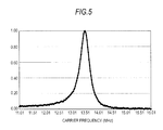
- Fig. 5 shows a frequency resonance characteristic in the antenna resonant circuit as an example.
- the frequency resonance characteristic is switched by changing, for example, the antenna capacity by a switch SW2 of the card 30, thereby increasing the power generated in the power generation unit 345.
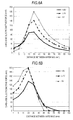
- Fig. 6A shows the relation between the electromotive force generated in the power generation unit 345 and the distance between antennas at respective operation voltages (5V, 3.3V and 1.8V) when the frequency resonance characteristic of the reader/writer 20 and the card 30 are as shown in Fig. 5 .
- Both the reader/writer 20 and the card 30 are designed so that the quality factor is high in the vicinity of the carrier frequency (13.56MHz) as a steep frequency resonance characteristic, the electromotive force becomes maximum when the distance between antennas is approximately 30mm. That is, as shown in Fig. 7A , the electromotive force becomes maximum when a person OM takes the card 30 in his hand and holds up to the reader/writer 20.
- Fig. 6B shows the relation between the electromotive force generated in the power generation unit 345 and distance between antennas at respective operation voltages (5V, 3.3V and 1.8V) when the frequency resonance characteristic is allowed to be approximately flat so as to be in a non-resonant state by making the quality factor of the card 30 to be lower than the characteristic shown in Fig. 5 .
- the electromotive force becomes maximum when an interval between the large antenna 21 of the reader/writer 20 and the large antenna 31 of the card 30 is approximately 20mm.
- the electromotive force is higher than Fig. 6A . That is, as shown in Fig. 7B , when content data is written in the card 30 from the host device 40 or when data written in the card 30 is read by the host device 40 in the state in which the reader/writer 20 is placed on the card 30, high electromotive power can be obtained.
- the antenna resonant circuit when the antenna resonant circuit is made to be the non-resonant state by reducing the quality factor, it is possible to increase power to be generated in the power generation unit 345 when the large antenna 21 of the reader/writer 20 and the large antenna 31 of the card 30 are in the close contact state.
- the switching of the frequency resonance characteristic is not limited to the case performed in the card 30 but it is also preferable that the switching is performed in the reader/writer 20.
- Fig. 8 shows a state in which high-speed communication is performed between the reader/writer 20 and the card 30.
- the card 30 is placed on the reader/writer 20 and negotiation is performed between the reader/writer 20 and the card 30 by using the electromagnetic induction system to thereby performing high-speed communication using the back scatter system.
- data communication is performed by transmitting a non-modulated carrier signal from the card 30, modulating the non-modulated carrier signal in accordance with the transmission signal and reflecting the signal in the reader/writer 20.
- the frequency resonance characteristic is changed from the characteristic (first characteristic) in which the quality factor is high to the characteristic (second characteristic) in which the frequency characteristic is allowed to be approximately flat by reducing the quality factor so that power to be generated in the power generation unit 345 is increased.
- Fig. 9 shows a sequence of communication operations.
- the reader/writer 20 when performing data communication with the card 30 at high speed, requests the card 30 to permit transmission by the electromagnetic induction system (ST1).
- the host device 40 supplies a communication control signal to the communication control unit 243 of the reader/writer 20 when transmitting data to the card 30.
- the communication control unit 243 controls operation of the low-speed communication processing unit 231 based on communication control information to transmit a modulated carrier signal indicating the request for transmission permission as a transmission signal from the large antenna 21.
- the communication control unit 243 supplies a non-modulated carrier signal to the large antenna 21 as the transmission signal until communication completion notification is supplied from the host device 40 so as to perform near-field wireless communication in the electromagnetic induction system.
- the power generation unit 345 When a reception signal, that is, the non-modulated carrier signal or the modulated carrier signal is obtained by the large antenna 31 of the card 30, the power generation unit 345 generates power from the carrier signal, supplying the generated power to respective units to operate the card 30.
- the low-speed communication processing unit 331 performs demodulation of the received modulated carrier signal and decoding of modulated data, supplying obtained reception data to the communication control unit 343. That is, the request transmission permission transmitted from the reader/writer 20 is supplied to the communication control unit 343.
- the card 30 makes a response of transmission permission when permitting communication using the high-speed communication processing unit 333 (ST2).
- the low-speed communication processing unit 331 performs coding and modulation of transmission data indicating the response of transmission permission to generate a transmission signal.
- the low-speed communication processing unit 331 also modulates the non-modulated carrier signal transmitted from the reader/writer 20 in accordance with the transmission signal.
- the low-speed communication processing unit 231 of the reader/writer 20 performs demodulation and decoding the carrier signal modulated in the card 30, supplying obtained reception data to the communication control unit 243. That is, the response of transmission permission transmitted from the card 30 is supplied to the communication control unit 243.
- the communication control unit 243 of the reader/writer 20 performs notification of communication control information based on the supply of the response of transmission permission from the card 30 (ST3).
- the communication control unit 243 of the reader/writer 20 supplies the communication control information supplied from the host device 40 to the low-speed communication processing unit 231.
- the low-speed communication processing unit 231 of the reader/writer 20 performs coding and modulation of the communication control information, generating a modulated carrier signal indicating the communication control information and transmitting the signal from the large antenna 21.
- the low-speed communication processing unit 331 of the card 30 receives the modulated carrier signal transmitted from the large antenna 31, performing demodulation and decoding of the modulated carrier signal, and supplying obtained reception data to the communication control unit 343. That is, the communication control information transmitted from the reader/writer 20 is supplied to the communication control unit 343.
- the communication control unit 343 of the card 30 performs setting of data communication by using the high-speed communication processing unit 333 based on the communication control information, radiating a non-modulated carrier signal as a radio signal from the small antenna 32 connected to the high-speed communication processing unit 333 so as to perform high-speed data communication with the reader/writer 20 (ST4).
- the communication control information includes information indicating data size
- data communication operation using the high-speed data communication unit can be completed when data reception of the size indicated by the communication control information is completed.
- the communication control unit 343 of the card 30 performs operation control of the high-speed communication processing unit 333 so that data communication can be performed with the reader/writer 20 in a transmission speed and a format indicated by the communication control information.
- the communication control unit 343 radiates a non-modulated carrier signal of, for example, 2.45GHz from the small antenna 32 so as to perform high-speed data communication with the reader/writer 20.
- the communication control unit 343 further changes the frequency resonance characteristic to the characteristic which is allowed to be approximately flat (second characteristic) by reducing the quality factor of the antenna resonant circuit of the large antenna 31 so as to obtain high power.
- the high-speed communication processing unit 233 of the reader/writer 20 performs data transmission by using the non-modulated carrier signal radiated from the card 30 (ST5).
- the communication control unit 243 of the reader/writer 20 writes transmission data supplied from the host device 40 in the buffer for high-speed communication 234 sequentially.
- the high-speed communication processing unit 233 reads transmission data written in the buffer for high-speed communication 234 sequentially, modulating the non-modulated carrier signal radiated from the card 30 and reflecting the signal based on the transmission signal generated by performing coding and modulation of the transmission data.
- the high-speed communication processing unit 333 of the card 30 receives a reflected-wave signal from the reader/writer 20, performing demodulation and decoding of the obtained reception signal, generating reception data and supplies the data to the communication control unit 343.
- the card 30 notifies the reader/writer 20 of reception completion when data communication of the size notified in advance is completed (ST6).
- the communication control unit 343 of the card 30 supplies the reception completion notification to the low-speed communication processing unit 331 when data communication of the size notified in advance is completed.
- the communication control unit 343 returns the frequency resonance characteristic of the antenna resonant circuit of the large antenna 31 to the first characteristic which is the previous frequency resonance characteristic in which the quality factor is high.
- the low-speed communication processing unit 331 performs coding and modulation of transmission data indicating the reception completion notification to generate a transmission signal.
- the low-speed communication processing unit 331 modulates the non-modulated carrier signal from the reader/writer 20 in accordance with the transmission signal. Further, the communication control unit 343 completes operation of the high-speed communication processing unit 333 to stop radiation of the non-modulated carrier signal when data communication is completed.
- the low-speed communication processing unit 231 of the reader/writer 20 performs demodulation and decoding of the carrier signal modulated in the card 30, supplying obtained reception data from the communication control unit 243 to the host device 40. That is, the reception completion notification transmitted from the card 30 to the host device 40.
- the host device 40 completes operation of the low-speed communication processing unit 231 of the reader/writer 20 to stop supply of the non-modulated carrier signal to the large antenna 21 when the reception completion notification is supplied.
- the control of processing of stopping the non-modulated carrier signal may be performed by the communication control unit 243.
- the card 30 switches the frequency resonance characteristic when performing the high-speed communication, thereby generating high power in the power generation unit 345 even when the large antenna 21 of the reader/writer 20 and the large antenna 31 of the card 30 are in the close contact state.
- the wireless communication device is applied to a playback device, and a playback device 30a, that is, the target including a content playback unit is placed on the reader/writer 20 and content data is supplied from the reader/writer 20 to the playback device 30a, playback of contents can be performed without providing a battery and the like at the playback device 30a. That is, the playback device of passive operation without the power supply can be realized.
- Fig. 10 shows a configuration of the playback device 30a as a target.
- the playback device 30a is provided with a large antenna 31 and a small antenna 32.
- the large antenna 31 is configured in the same manner as the large antenna 21 of the reader/writer 20, which is connected to the low-speed communication processing unit 331 and the power generation unit 345 in the card control unit 33a.
- the small antenna 32 is configured in the same manner as the small antenna 22 of the reader/writer 20, which is connected to the high-speed communication processing 333 in the card control unit 33a.
- the low-speed communication processing unit 331 performs coding processing of transmission data read from the buffer for low-speed communication 332, modulation processing of coded data obtained by performing the coding processing and the like.
- the low-speed communication processing unit 331 generates a transmission signal by performing these processing and supplies the signal to the large antenna 31.
- the low-speed communication processing unit 331 performs demodulation processing of a reception signal obtained by the large antenna 31, decoding processing of the demodulated signal obtained by performing the demodulation processing and the like.
- the low-speed communication processing unit 331 stores reception data obtained by performing these processing in the buffer for low-speed communication 332.
- the buffer for low-speed communication 332 is a buffer for temporarily storing reception data supplied from the low-speed communication processing unit 331 and transmission data supplied from the communication control unit 343.
- the high-speed communication processing unit 333 performs coding processing of transmission data read from the buffer for high-speed communication 334, modulation processing of coded data obtained by performing the coding processing and the like.
- the high-speed communication processing unit 333 generates a transmission signal by performing these processing and supplies the signal to the small antenna 32.
- the high-speed communication processing unit 333 also performs demodulation processing of a reception signal obtained by the small antenna 32, decoding processing of the demodulated signal obtained by performing the demodulation processing and the like.
- the high-speed communication processing unit 333 stores reception data obtained by performing these processing in the buffer for high-speed communication 334.
- the high-speed communication processing unit 333 transmits a non-modulated carrier signal from the small antenna 32.
- the high-speed communication processing unit 333 generates reception data by performing demodulation processing and the like of the modulated carrier signal obtained by receiving reflected waves from the reader/writer 20 by the small antenna 32.
- the buffer for high-speed communication 334 is a buffer for temporarily storing reception data supplied from the high-speed communication processing unit 333 and transmission data supplied from the communication control unit 343.
- a content data processing unit 335 generates a playback signal by reading content data supplied from the reader/writer 20 through the small antennas 22, 32 from the buffer for high-speed communication 334 and processing the data.
- the content data processing unit 335 performs expansion/decoding processing and the like as the processing, for example, when content data read from the buffer for high-speed communication 334 is compressed/coded.
- a content playback unit 336 performs playback of a content by using the playback signal generated in the content data processing unit 335. For example, when the playback signal is a signal of a video content, a video display is performed based on the playback signal. When the playback signal is a signal of an audio content, audio output is performed based on the playback signal.
- the communication control unit 343 is connected to the low-speed communication processing unit 331, the buffer for low-speed communication 332, the high-speed communication processing unit 333, the buffer for high-speed communication 334, the content data processing unit 335 and the content playback unit 336 through the bus 346.
- the communication control unit 343 performs communication with the reader/writer 20, receiving content data transmitted from, for example, the reader/writer 20, and performing video display and audio output by the content playback unit 336 based on the received content data.
- the power generation unit 345 performs rectification, smoothing, voltage conversion and the like to the carrier signal received by the large antenna 31 to generate power which is a prescribed direct-current voltage.
- the power generation unit 345 further supplies generated power to respective units of the playback unit 30a.
- Fig. 11A shows a case in which content data of a video content is transmitted from the reader/writer 20 to the playback device 30a to perform video display in the content playback unit 336 of the playback device 30a.
- the communication control unit 343 of the playback device 30a when performing playback of content data, switches the frequency resonance characteristic of the large antenna 31 to the characteristic which is approximately flat to be a non-resonant state by reducing the quality factor so as to obtain high power.
- the playback device 30a performs communication of content data with the reader/writer 20 by using the small antenna 32, storing reception data obtained by the high-speed communication processing unit 333 in the buffer for high-speed communication 334.
- the content data processing unit 335 generates a content playback signal by reading reception data stored in the buffer for high-speed communication 334 sequentially and performing expansion processing and the like.
- the content data processing unit 335 supplies the generated content playback signal to the content playback unit 336.
- the content playback unit 336 is configured by using a liquid crystal display device, an organic EL display device and the like.
- the content playback unit 336 performs video display based on the content playback signal.
- Fig. 11B shows a case in which content data of an audio content is transmitted from the reader/writer 20 to the playback device 30a and audio output is performed in the content playback unit 336 of the playback device 30a.
- the communication control unit 343 of the playback device 30a when performing playback of content data, switches the frequency resonance characteristic of the large antenna 31 to the characteristic which is approximately flat to be a non-resonant state by reducing the quality factor so as to obtain high power.
- the playback device 30a stores reception data in the buffer for high-speed communication 334, which is obtained by the high-speed communication processing unit 333 when performing communication with the reader/writer 20 by using the small antenna 32.
- the content data processing unit 335 generates a content playback signal by reading reception data stored in the buffer for high-speed communication 334 sequentially, performing expansion processing and the like.
- the content data processing unit 335 supplies the generated content playback signal to the content playback unit 336.
- the content playback unit 336 is configured by using a speaker and the like.
- the content playback unit 336 performs audio output from the speaker based on the content playback signal.
- the playback device 30a When the playback device 30a is provided with a tuner in addition to the display device, the speaker and the like, it is possible to view television programs and the like.
- the playback device 30a is provided with a memory unit and a memory processing unit which performs writing/reading of data with respect to the memory unit, in which content data transmitted from the reader/writer 20 in the memory unit.
- the playback device 30a can play back contents stored in the memory unit by supplying power from the reader/writer 20 to the playback device 30a even when the playback device 30a does not acquire content data by performing communication with the reader/writer 20.
- the playback device 30a can perform video display and audio output in a state of being placed on the reader/writer 20 without providing a battery in the playback device 30a. Since the playback device 30a can perform data communication and power supply in a non-contact manner, it is not necessary to form an opening and the like for a connection interface. Therefore, it is possible to provide the playback device 30a which is dustproofed and waterproofed simply and easily. It is also not necessary to provide a power supply unit and a communication interface unit in the playback device 30a. Therefore, it is easy to allow the playback device 30a to be light in weight and thin in thickness. The playback device 30a also does not have a mechanical structure or a contact point. Therefore, it is possible to provide the playback device 30a which is trouble free and reliable. Additionally, the playback device 30a can have a user interface function by the device itself by using a touch panel and the like as an internal device.
- the frequency resonance characteristic in the playback device 30a can be switched between the first characteristic in which the quality factor is high as in related arts and the second characteristic in which the frequency characteristic is allowed to be approximately flat by reducing the quality factor so as to generate higher power, thereby having various mode functions.
- the frequency resonance characteristic of the large antenna is the first characteristic when, for example, in an existing close communication compatibility mode.
- the playback device 30a stores identification information or individual information and the like unique to the user in the memory. According to this, it is possible that the playback device 30a can perform communication in the same distance as the IC card and the like having the existing close communication function and can be used as an individual authentication or an electronic payment card compatible with the NFCIP-1.
- the playback device 30a performs negotiation in the NFCIP-1 type communication and performs high-speed communication using the small antenna in a large-capacity high-speed storage mode.
- the playback device 30a switches the frequency resonance characteristic of the large antenna 31 from the previous characteristic to the characteristic in which high power can be generated even in the close contact state. According to this, the playback device 30a can obtain high power even when the device and the reader/writer 20 are in the close contact state, therefore, it is possible to perform high-speed communication, for example, by transmitting a non-modulated carrier signal from the small antenna 32 of the playback device 30a.
- the received data signal is stored in the memory.
- the buffer for the high-speed communication 334 may also be used as the memory. It is also preferable that the playback device 30a maintains the frequency resonance characteristic of the large antenna 31 in the state of the first characteristic of related arts when the power necessary for high-speed communication is low.
- the playback device 30a performs negotiation in the NFCIP-1 type communication and switches the frequency resonance characteristic of the large antenna 31 from the previous first characteristic to the second characteristic in which high power can be generated in the close contact state in an AV device mode. According to this, the playback device 30a can obtain high power, therefore, it is possible to perform video display and audio output by operating the content data processing unit, the content playback unit and the like. It is also preferable that content data stored in the memory is used as content data used for playback, and that content data is acquired from the reader/writer 20 by performing high-speed communication by using the small antenna.
- the frequency resonance characteristic of the antenna unit is changed as described above, thereby increasing power generated in the power generation unit 345 when the large antenna 21 of the reader/writer 20 and the large antenna 31 of the card 30 are in the close contact state. Therefore, for example, when the wireless communication device is provided as a power receiving device with respect to a power supply module configured by using a battery, it is possible to perform charging of a target which is a power supply module 30b by using power generated in the power generation unit 345.
- Fig. 13 shows a configuration of the power supply module 30b as the target.
- the power supply module 30b is provided with the large antenna 31 and the small antenna 32.
- the large antenna 31 is configured in the same manner as the large antenna 21 of the reader/writer 20, which is connected to the low-speed communication processing unit 331 and the power generation unit 345 in the card control unit 33b.
- the small antenna 32 is configured in the same manner as the small antenna 22 of the reader/writer 20, which is connected to the high-speed communication processing 333 in the card control unit 33b.
- the low-speed communication processing unit 331 performs coding processing of transmission data read from the buffer for low-speed communication 332, modulation processing of coded data obtained by performing coding processing and the like.
- the low-speed communication processing unit 331 generates a transmission signal by performing these processing and supplies the signal to the large antenna 31.
- the low-speed communication processing unit 331 also performs demodulation processing of a reception signal obtained by the large antenna 31, decoding processing of the demodulated signal obtained by performing the demodulation processing and the like.
- the low-speed communication processing unit 331 stores reception data obtained by performing these processing in the buffer for low-speed communication 332.
- the buffer for low-speed communication 332 is a buffer for temporarily storing reception data supplied from the low-speed communication processing unit 331 and transmission data supplied from the communication control unit 343.
- the high-speed communication processing unit 333 performs coding processing of transmission data read from the buffer for high-speed communication 334, modulation processing of coded data obtained by performing the coding processing and the like.
- the high-speed communication processing unit 333 generates a transmission signal by performing these processing and supplies the signal to the small antenna 32.
- the high-speed communication processing unit 333 also performs demodulation processing of a reception signal obtained by the small antenna 32, decoding processing of the demodulated signal obtained by performing demodulation processing and the like.
- the high-speed communication processing unit 333 stores reception data obtained by performing these processing in the buffer for high-speed communication 334.
- the high-speed communication processing unit 333 transmits a non-modulated carrier signal from the small antenna 32.
- the high-speed communication processing unit 333 also generates reception data by performing demodulation processing of the modulated carrier signal obtained by receiving reflected waves from the reader/writer 20 by the small antenna 32.
- the buffer for high-speed communication 334 is a buffer for temporarily storing reception data supplied from the high-speed communication processing unit 333 and transmission data supplied from the communication control unit 343.
- a memory control unit 337 performs processing of reading reception data stored in the buffer for high-speed communication 334 and writing the data in a memory unit 338, and processing of reading data stored in the memory unit 338 and temporarily storing the data in the buffer for high-speed communication 334 as transmission data.
- An internal power supply unit 340 using a secondary battery is connected to a power supply management unit 339.
- the power management unit 339 detects the remaining amount of the battery of the internal power supply unit 340, generating power supply information indicating the detection result and supplying the information to the buffer for low-speed communication 332 and the buffer for high-speed communication 334.
- the internal power supply unit 340 supplies power to respective units in the power supply module 30b.
- the internal power supply unit 340 performs charging of a battery by using power generated in the connected power generation unit 345.
- the communication control unit 343 is connected to the low-speed communication processing unit 331, the buffer for low-speed communication 332, the high-speed communication processing unit 333 and the buffer for high-speed communication 334 through the bus 346.
- the communication control unit 343 performs processing in accordance with reception data, for example, performing processing of reading requested information from the memory unit and generating a transmission signal to be transmitted, processing of generating a transmission signal indicating power supply information and transmitting the signal.
- the power generation unit 345 performs rectification, smoothing, voltage conversion and the like to the carrier signal received by the large antenna 31 to generate power which is a prescribed direct-current voltage. Further, the power generation unit 345 supplies the generated power to the internal power supply unit 340.
- the wireless communication device is provided only as the power receiving device, it is not always necessary to have the high-speed communication processing unit 333 and the buffer for high-speed communication 334.
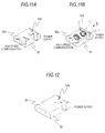
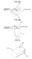
- Fig. 14A is a view for explaining operations when charging the power supply module 30b.
- the power supply module 30b is placed on the reader/writer 20 so that the large antenna 31 faces the large antenna 21 of the reader/writer 20.
- the communication control unit 343 switches the frequency resonance characteristic of the large antenna 31 to the second characteristic which is allowed to be approximately flat by reducing the quality factor so as to increase power generated in the power generation unit 345.
- the power supply module 30b performs communication with the reader/writer 20 by using the small antenna 32, thereby storing reception data stored in the buffer for high-speed communication 334 in the memory unit 338 by the memory control unit 337 when receiving content data and the like.
- the power generation unit 345 performs power generation by using the carrier signal received by the large antenna 31, supplying the generated power to the internal power supply unit 340.
- the internal power supply unit 340 charges the battery by using power supplied from the power generation unit 345.
- Fig. 14B is a view for explaining operations when performing power supply with respect to an external device 45 from the power supply module 30b.
- the antennas and communication processing units performing communication with the power supply module 30b are configured in the same manner as the reader/writer 20.
- the external device 45 is provided with the power generation unit which generates power from the carrier signal received by the large antenna.
- the power supply module 30b When performing power supply with respect to the external device 45 from the power supply module 30b, the power supply module 30b is placed on the external device 45 so that the large antenna 31 faces the large antenna 21 of the external device 45.
- the external device 45 receives the carrier signal transmitted from the large antenna 31 of the power supply module 30b and generates power from the received carrier signal.
- the external device 45 also charges the internal battery by using the generated power. Further, the external device 45 performs various operations by using the generated power when there is not provided a battery, or when the battery has been charged.
- the power supply module 30b performs communication with the external device 45 by using the small antenna 32, transmitting content data and the like stored in the memory unit 338 to the external device 45. It is also preferable that the power supply module 30b transmits information indicating the remaining amount of the battery and authentication information for identifying whether it is a normal power supply module to the external device 45.
- the power supply module 30b can obtain various advantages by performing charging of the internal power supply unit 340 by power generated by communication with the reader/writer 20 through the large antenna. That is, the power supply module has relatively large space inside the module due to the nature thereof (components of a power supply circuit are large, tight integration is difficult because of heat release and so on), therefore, it is possible to save space on the side of the external device by mounting a memory for the external device in vacant space.
- the power supply module 30b itself has communication functions, it is possible to secure power necessary for transmitting the carrier for high-speed communication, therefore, the power supply module 30b can transmit data stored in the mounted memory for the external device to the external device.
- the power supply module 30b can execute all of the near-field wireless communication, power discharge (at the time of driving the external device) and power supply (at the time of charging), therefore, it is not necessary to provide an opening for a connection interface at the module itself. Accordingly, it is possible to provide the power supply module 30b which is dustproofed and waterproofed simply and easily.
- the power supply module 30a also does not have a mechanical structure or a contact point. Therefore, it is possible to provide the reliable power supply module 30b which is corrosion-free, deterioration-free, trouble-free and the like. It is also possible to transmit information of the battery remaining amount, authentication indicating the normal battery by the non-contact communication.
- Fig. 15 shows a case in which the playback device 30a is placed on the power supply module 30b and performs communication with the power supply module 30b.
- the playback device 30a is, for example, a display-type (with a touch panel) playback device with passive operation.
- the playback device 30a performs communication with the power supply module 30b, thereby acquiring information concerning the power supply state (remaining amount) of the power supply included in the power supply module 30b, the contents of the memory and the like, and displaying the information on a display unit with the touch panel 341.
- the playback device 30a When the display unit with the touch panel 341 is operated, the playback device 30a generates a command signal in accordance with the operation and supplies the command to the power supply module 30b to thereby reading data stored in the memory of the power supply module 30b.
- the power supply module 30b not only can supply power and supply content data to the playback device 30a but also can receive power and content data from the reader/writer 20.
- Fig. 16A shows a configuration of the power supply module 30b in a case in which the large antenna 31 and the small antenna 32 are provided at two facing surfaces respectively.
- Fig. 16B shows a configuration when the playback device 30a is placed on the power supply module 30b having the antennas at both surfaces.
- the power supply module 30b performs high-speed communication with the playback device 30a.
- the power supply module 30b transmits a carrier signal from the large antenna by using power supplied from the internal battery to thereby operate the playback device 30a.
- the power supply module 30b performs high-speed communication of content data stored in the internal memory, playing back the transmitted content data in the playback device 30a. Accordingly, the power supply module 30b functions as an external power supply as well as a high-speed storage device of the playback device 30a.
- a holding mechanism which holds the playback device 30a and the power supply module 30b in a combined state is provided to allow the large antennas of the playback device 30a and the power supply module 30b to be in the closed contact state. It is possible to carry the playback device 30a and the power supply module 30b in the combined state easily by providing such mechanism.
- Fig. 16C shows a case in which the power supply module 30b is placed on the reader/writer 20 in a state in which the playback device 30a is placed on the power supply module 30b having the antennas at both surfaces.
- the power supply module 30b charges the internal battery by using power supplied from the reader/writer 20.
- the power supply module 30b transmits a carrier signal from the large antenna by using power supplied from the internal battery, thereby operation the playback device 30a. It is also preferable that the power supply module 30b transmits a carrier signal from the large antenna by using power supplied from the reader/writer 20.
- the power supply module 30b store content data supplied from the reader/writer 20 in the internal memory.
- the power supply module 30b performs high-speed communication of content data stored in the internal memory to play back transmitted content data in the playback device 30a. It is also possible that the power supply module 30b transmits content data supplied from the reader/writer 20 to the playback device 30a.
- Fig. 16D shows a configuration of a case in which the power supply module 30b is removed. In this case, operation will be the one of the above-described second embodiment. Also in the cases shown in Fig. 16C and Fig. 16D , when there is provided the holding mechanism which holds the reader/writer 20, the playback device 30a and the power supply module 30b in the combined state, it is possible to carry them in the combined state easily.
- the wireless communication device and the power receiving device of the embodiments of the invention it is possible to perform communication and the like by receiving sufficient power even when the near-field wireless communication is performed in a state in which antennas of the transmission-side and the receiving-side wireless communication devices are in the close contact state. Accordingly, the invention can be applied to not only the IC card used as individual authentication, electronic money payment and the like but also the playback device which plays back video and audio contents, the power supply module and the like.
Landscapes
- Engineering & Computer Science (AREA)
- Computer Networks & Wireless Communication (AREA)
- Power Engineering (AREA)
- Artificial Intelligence (AREA)
- Computer Vision & Pattern Recognition (AREA)
- Physics & Mathematics (AREA)
- General Physics & Mathematics (AREA)
- Theoretical Computer Science (AREA)
- Signal Processing (AREA)
- Near-Field Transmission Systems (AREA)
Abstract
Description
- The invention relates to a wireless communication device and a power receiving device. Particularly, the invention relates to the wireless communication device and the power receiving device capable of performing communication and the like while obtaining sufficient power even when communication is performed in a state in which antennas of transmission-side and receiving-side wireless communication devices make contact with each other closely.
- In related arts, an NFCIP-1 (Near Field Communication Interface and Protocol-1) standard is provided as an international standard of near-field wireless communication. A reader/writer and an IC card complying with the NFCIP-1 standard are broadly used for individual authentication, electronic money payment and the like.
- In data communication using a type complying with the NFCIP-1 standard (hereinafter, referred to as an "NFCIP-1 type"), a passive communication mode and an active communication mode by 13.56MHz electromagnetic induction coupling are prescribed. In the passive communication mode, a non-modulated carrier signal is transmitted from the reader/writer to the IC card. The IC card modulates the transmitted non-modulated carrier signal in accordance with data to be transmitted. The reader/writer obtains data transmitted from the IC card by performing demodulation and the like of the modulated carrier signal. Accordingly, in the passive communication mode, communication is performed without generation of the carrier signal by the IC card itself. Also in the passive communication mode, power generation is performed by using the carrier signal transmitted from the reader/writer and operations of the IC card are performed by using the generated power.
- On the other hand, in the active communication mode, the IC card itself generates the carrier signal, modulates the generated carrier signal in accordance with data to be transmitted, then, transmits the signal. The reader/writer performs demodulation and the like of the modulated carrier signal, thereby obtaining data transmitted from the IC card. Accordingly, in the active communication mode, for example, as in
JP-A-2005-323264 - In the case of the passive communication mode, it is assumed that main applications of the IC card used for the near-field wireless communication are individual authentication (for example, at an entrance gate), electronic money payment (for example, at a vending machine" and the like, therefore, the IC card is designed so that communication stability can be obtained maximally when the IC card is carried by a human hand, for example, when the reader/writer and the IC card is several centimeters apart from each other. Accordingly, it is difficult to obtain stable power in conditions different from the case in which the card is operated by a human hand. For example, when communication of video contents or audio contents is performed by using the reader/writer and the IC card, the IC card is placed on the reader/writer in a state of touching the reader/writer, therefore, it is difficult to obtain stable power.
- Additionally, it is necessary to provide the power supply unit using the primary battery or the secondary battery in the active communication mode, therefore, when the remaining amount of the battery is reduced, battery change or charging by connecting the IC card to a charger is necessary.
- Thus, it is desirable to provide a wireless communication device and a power receiving device capable of performing communication and the like while obtaining sufficient power even when antennas of transmission-side and receiving-side wireless communication devices are in a close contact state.
- According to an embodiment of the invention, there is provided a wireless communication device including a first communication processing unit performing communication in an electromagnetic induction system by using a first antenna unit, a second communication processing unit performing communication at higher speed than the first communication processing unit by a system or a communication frequency different from the electromagnetic induction system by using a second antenna unit, and a power generation unit generating power at least for performing communication operations from a carrier signal received by the first antenna unit, in which the power is generated in the power generation unit by switching a frequency resonance characteristic of the first antenna unit.
- In the embodiment of the invention, communication in the electromagnetic induction system, for example, an NFCIP-1 type communication is performed in the first communication processing unit by using the first antenna unit. Also, communication higher than the first communication processing unit is performed in the second communication processing unit in a system different from the electromagnetic induction system, for example, a back scatter system by using the second antenna unit. Furthermore, power at least for performing communication operations is generated in the power generation unit from the carrier signal received in the first antenna unit. The first antenna unit is used in close contact state with the transmission-source antenna unit which transmits the carrier signal. The first communication processing unit allows the frequency resonance characteristic of the first antenna unit, for example, a quality factor in an antenna resonant circuit to be high when data communication is performed as well as allows the quality factor to be lower than the time of performing data communication when data communication is not performed, accordingly, power is generated in the power generation unit. Additionally, a content playback unit performing playback of contents is provided, in which the power generation unit supplies generated power to the content playback unit. Furthermore, a power supply unit which can be charged is provided, in which the power generation unit charges the power supply unit by using generated power to supply power at least for performing communication operations from the power supply unit.
- According to another embodiment of the invention, there is provided a power receiving device including a power generation unit generating power from a carrier signal received by an antenna unit for performing data communication in an electromagnetic induction system, in which power is generated in the power generation unit by switching a frequency resonance characteristic of the antenna unit in accordance with data communication operation in the electromagnetic induction system.
- According to the embodiment of the invention, power is generated in the power generation unit from the carrier signal received by the antenna unit for performing communication in the electromagnetic induction system, for example, the NFCIP-1 type communication. When data communication is performed in the electromagnetic induction system, the frequency resonance characteristic in the antenna portion, for example, the quality factor in the antenna resonant circuit is allowed to be high. When data communication is not performed, the quality factor is allowed to be lower than the time of performing data communication. The antenna unit is used in a close contact with the transmission-source antenna unit which transmits the carrier signal.
- According to the embodiments of the invention, power is generated in the power generation unit which generates power from the carrier signal received by the antenna unit for performing data communication in the electromagnetic induction system by switching the frequency resonance characteristic of the antenna unit . Accordingly, it is possible to perform near-field wireless communication and the like while obtaining sufficient power even when antennas of transmission-side and receiving-side wireless communication devices are in the close contact state.
-
-
Fig. 1 is a diagram showing a configuration of a wireless communication system; -
Fig. 2 is a view showing antenna shapes; -
Fig. 3 is a view showing arrangement of a reader/writer and a card; -
Fig. 4 is a view showing antenna configurations of the reader/writer and the card; -
Fig. 5 is a graph showing a frequency resonance characteristic of an antenna unit as an example; -
Fig. 6A and Fig. 6B are graphs showing the relation between the electromotive force and the distance between antennas; -
Fig. 7A and Fig. 7B are views showing the positional relation between the reader/writer and the card; -
Fig. 8 is a view showing a state in which high-speed communication is performed between the reader/writer and the card; -
Fig. 9 is a diagram showing a sequence of communication operations; -
Fig. 10 is a diagram showing a configuration of a playback device; -
Fig. 11A and Fig. 11B are views for explaining operations of the playback device; -
Fig. 12 is a view for explaining another operation of the playback device; -
Fig. 13 is a diagram showing a configuration of a power supply module, -
Fig. 14A and Fig. 14B are views for explaining operations when using the power supply module; -
Fig. 15 is a view showing a usage pattern of the power supply module as an example; and -
Fig. 16A to Fig. 16D are views showing other usage patterns of the power supply module as examples. - A wireless communication system using a wireless communication device according to an embodiment includes, for example, an initiator and a target complying with near-field wireless communication, in which a first antenna unit used for data communication of related art near-field wireless communication, for example, an NFCIP-1 type and a second antenna unit for performing communication at higher speed than near-field wireless communication using the first antenna unit are provided to thereby improving communication speed in the whole system. Further, power is generated from a carrier signal received by the first antenna unit, thereby performing high-speed communication and processing of communication data, charging of a battery and the like by the generated power. Hereinafter, the best mode for carrying out the invention (hereinafter, embodiments) will be explained. The explanation will be made in the following order.
- 1. First Embodiment
- 2. Second Embodiment (a case of performing playback of contents by using generated power)
- 3. Third Embodiment (a case of performing charging by using generated power)
-
Fig. 1 shows a configuration of a wireless communication system according to an embodiment of the invention. Awireless communication system 10 includes aninitiator 20 which starts communication and atarget 30 to be a target of the communication. - The
initiator 20 is specifically a reader/writer (R/W) complying with near-field wireless communication operating in a reader/writer mode. The reader/writer as theinitiator 20 is connected to ahost device 40 through a host interface such as a UART (Universal Asynchronous receiver-transmitter). Thehost device 40 corresponds to a personal computer (PC) or an integrated CPU (Central Processing Unit) inside the reader/writer, which performs generation of transmission data, processing of reception data, generation of communication control signals for controlling communication operations and the like. - The
target 30 is a transponder such as the IC card complying with the near-field wireless communication or a reader/writer complying with near-field wireless communication operating in a card mode (hereinafter, these targets are referred to as merely "cards") . The card (target) 30 may be a standalone-type or may be connected to ahost device 41. - The reader/writer (initiator 20) is provided with a
first antenna unit 21 and asecond antenna unit 22. The card (target) 30 is provided with afirst antenna unit 31 and asecond antenna unit 32.Fig. 2 shows antenna shapes. When thecard 30 has a shape of, for example, 85.6mm×54.0mm which is prescribed by ISO/IEC7816-2, JIS6301-2 standards and the like, the first antenna unit 21 (31) and the second antenna unit 22 (32) are provided within an area ARc of the card size. - The first antenna unit 21 (31) used for data communication of the related-art near-field wireless communication, for example, the NFCIP-1 type communication is formed by a rectangular antenna coil formed along an outer periphery of the card area. The second antenna unit 22 (32) used for high-speed communication can perform data communication independently without causing mutual interference with respect to communication using the first antenna unit, which is provided, for example, at the center of the card area ARc so as not to interfere with power supply from the reader/
writer 20 to thecard 30 by the first antenna unit. A control IC chip SC is an integrated circuit of an antenna tuning circuit, a later-describedcard control unit 33 of thecard 30 and the like, to which the first antenna unit and the second antenna unit are connected. In the following description, thefirst antenna unit 21 is called as a large antenna and asecond antenna unit 22 is called as a small antenna. - The
large antenna 21 is connected to a communication processing unit (hereinafter, referred to as a "low-speed communication processing unit) 231 for performing data communication of the related-art near-field wireless communication, for example, the NFCIP-1 type communication. Thesmall antenna 22 is connected to a communication processing unit (hereinafter, referred to as a "high-speed communication processing unit) 233 for performing high-speed communication. - The low-speed
communication processing unit 231 of a reader/writer control unit 23 performs coding processing of transmission data read from a buffer for low-speed communication 232, modulation processing of coded data obtained by performing the coding processing and the like so as to perform NFCIP-1 type data communication in the same manner as the related art by using theantenna 21. The low-speedcommunication processing unit 231 generates a transmission signal by performing these processing and supplies the signal to thelarge antenna 21. The low-speedcommunication processing unit 231 also performs demodulation processing of a reception signal obtained by thelarge antenna 21, decoding processing of the demodulated signal obtained by performing the demodulation processing and the like. The low-speedcommunication processing unit 231 stores reception data obtained by performing these processing in the buffer for low-speed communication 232. - Table 1 shows a transfer direction in the NFCIP-1 type, communication speed, a carrier frequency, a modulation scheme, and a coding scheme with respect to respective communication modes. For example, when a communication system of Felica (trademark) as the NFCIP-1 type data communication is used, the low-speed
communication processing unit 231 performs ASK modulation/demodulation processing, Manchester coding/decoding processing and the like.Table 1 Transfer direction A type B type Felica Communication speed 106kb/s 106kb/s 212kb/s 424kb/s R/W→Card Carrier frequency 13.56MHz 13.56MHz 13.56 MHz Modulation scheme 100 %ASK 10%ASK 8-30%ASK Coding scheme Deformed mirror NRZ Manchester Card→R/W Subcarrier frequency 13.56MHz/16 13.56MHz/16 - Modulation scheme Load modulation Load modulation >12%ASK load modulation Coding scheme Manchester BPSK-NRZ-L Manchester - The buffer for low-
speed communication 232 is a buffer for temporarily storing reception data supplied from the low-speedcommunication processing unit 231 and transmission data supplied from acommunication control unit 243. - The high-speed
communication processing unit 233 performs communication at higher speed than the NFCIP-1 type data communication by using thesmall antenna 22. The high-speedcommunication processing unit 233 performs coding processing of transmission data read from a buffer for high-speed communication 234, modulation processing of coded data obtained by performing the coding processing and the like. The high-speedcommunication processing unit 233 generates a transmission signal by performing these processing and supplies the signal to thesmall antenna 22. The high-speedcommunication processing unit 233 also performs demodulation processing of a reception signal obtained by thesmall antenna 22, decoding processing of the demodulated signal obtained by performing the demodulation processing and the like. The high-speedcommunication processing unit 233 stores reception data obtained by performing these processing in the buffer for high-speed communication 234. - The high-speed
communication processing unit 233 performs a back scatter system, a communication system called as a weak UWB (Ultra Wide Band) using a communication frequency band of 4.48GHz, a baseband broadband communication in the electromagnetic induction system and the like as the communication system which is higher than the NFCIP-1 type data communication. When using the above systems, data communication at higher speed than the NFCIP-1 type can be performed as shown in Table 2.Table 2 NFCIP-1 system (Felica) Back scatter system Weak UWB system Carrier center frequency 13.56MHz 2.4GHz 4.48GHz Power-consumption Transmission 100mW to 199mW 600mW approx.100mW Reception Several mW 30mW approx.160mW Transfer rate up to 424kb/s Several Mb/s (Active)
Several dozen Mb/s
(Reflective)375Mb/s (Effective) Communication range up to 10cm Several cm assumed to be within 3cm - For example, when the back scatter system is used, the high-speed
communication processing unit 233 performs ASK modulation/demodulation processing or PSK modulation/demodulation processing, NRZ-L coding/decoding processing and the like. The high-speedcommunication processing unit 233, when transmitting the generated transmission signal, modulates a non-modulated carrier signal supplied from thesmall antenna 32 of thecard 30 in accordance with the transmission signal and reflects the signal. The high-speedcommunication processing unit 233 also generates reception data by receiving the modulated carrier signal supplied from thesmall antenna 32 of thecard 30 and performing demodulation and the like. - The buffer for high-
speed communication 234 is a buffer for temporarily storing reception data supplied from the high-speedcommunication processing unit 233 and transmission data supplied from thecommunication control unit 243. - The
communication control unit 243 is connected to the low-speedcommunication processing unit 231, the buffer for low-speed communication 232, the high-speedcommunication processing unit 233 and the buffer for high-speed communication 234 through abus 236. Thecommunication control unit 243 is also connected to thehost device 40. Thecommunication control unit 243 controls operations of respective units based on communication control signals from thehost device 40 to perform communication with the card (target) 30 by using thelarge antenna 21 and thesmall antenna 22. - The
card 30 is provided with thelarge antenna 31 and thesmall antenna 32. Thelarge antenna 31 is configured in the same manner as thelarge antenna 21 of the reader/writer 20, which is connected to a low-speedcommunication processing unit 331 and apower generation unit 345 in thecard control unit 33. Thesmall antenna unit 32 is configured in the same manner as thesmall antenna 22 of the reader/writer 20, which is connected to the high-speedcommunication processing unit 333 in thecard control unit 33. - The low-
speed communication unit 331 performs coding processing of transmission data read from the buffer for the low-speed communication 332, modulation processing of coded data obtained by performing the coding processing and the like. The low-speedcommunication processing unit 331 generates a transmission signal by performing these processing and supplies the signal to thelarge antenna 31. The low-speedcommunication processing unit 331 performs demodulation processing of a reception signal obtained by thelarge antenna 31, decoding processing of the demodulated signal obtained by performing the demodulation processing and the like. The low-speedcommunication processing unit 331 stores reception data obtained by performing these processing in the buffer for low-speed communication 332. - The buffer for low-
speed communication 332 is a buffer for temporarily storing reception data supplied from the low-speedcommunication processing unit 331 and transmission data supplied from acommunication control unit 343. - The high-speed
communication processing unit 333 performs coding processing of transmission data read from the buffer for high-speed processing 334, modulation processing of coded data obtained by performing the coding processing and the like. The high-speedcommunication processing unit 333 generates a transmission signal by performing these processing and supplies the signal to thesmall antenna 32. The high-speedcommunication processing unit 333 also performs demodulation processing of a reception signal obtained by thesmall antenna 32, decoding processing of the demodulated signal obtained by performing demodulation processing and the like. The high-speedcommunication processing unit 333 stores reception data obtained by performing these processing in the buffer for high-speed processing 334. - The high-speed
communication processing unit 333, when using, for example, the back scatter system, transmits a non-modulated carrier signal from thesmall antenna 32. The high-speedcommunication processing unit 333 generates reception data by performing demodulation processing and the like of the modulated carrier signal obtained by receiving reflected waves from the reader/writer 20. Further, the high-speedcommunication processing unit 333, when generating a transmission signal and transmitting the signal, modulates the carrier signal in accordance with the transmission signal and transmits the signal from thesmall antenna 32. - The buffer for high-
speed communication 334 is a buffer for temporarily storing reception data supplied from the high-speedcommunication processing unit 333 and transmission data supplied from thecommunication control unit 343. - The
communication control unit 343 is connected to the low-speedcommunication processing unit 331, the buffer for low-speed communication 332, the high-speedcommunication processing unit 333 and the buffer for high-speed communication 334 through abus 346. Thecommunication control unit 343 performs processing in accordance with reception data, performing processing of reading, for example, requested information from a nonvolatile memory (not shown) and generating a transmission signal. When thecommunication control unit 343 is connected to thehost device 41, thecommunication control unit 343 controls operations of respective units based on communication control signals from thehost device 41 to perform communication with the reader/writer (initiator) 20 by using thelarge antenna 31 and thesmall antenna 32. - The
power generation unit 345 performs rectification, smoothing, voltage conversion and the like to the carrier signal received by thelarge antenna 31 to generate power which is a prescribed direct-current voltage. Thepower generation unit 345 further supplies generated power to respective units of thecard 30. - In the
wireless communication system 10 configured as the above, as shown inFig. 3 , data communication is performed by providing thecard 30 with respect to the reader/writer 20 so that thelarge antenna 21 of the reader/writer 20 faces thelarge antenna 31 of thecard 30 as well as thesmall antenna 22 of the reader/writer 20 faces thesmall antenna 32 of thecard 30, respectively. When the reader/writer 20 and thecard 30 are in a close contact state, a frequency resonance characteristic in an antenna resonant circuit of the large antenna 21 (or the large antenna 31) is switched so that generated power will be high. -
Fig. 4 shows antenna configurations of thelarge antenna 21 of the reader/writer 20 and thelarge antenna 31 of thecard 30. Thelarge antenna 21 of the reader/writer 20 includes an antenna coil and a resonant circuit, and an equivalent circuit of thelarge antenna 21 is shown as an antenna resonant circuit ECa. Thelarge antenna 31 of thecard 30 includes an antenna coil, a resonant circuit and a load switching modulation circuit for performing amplitude modulation, and an equivalent circuit showing the antenna coil and the resonant circuit is shown as an antenna resonant circuit ECb. - The antenna resonant circuit ECa of the reader/
writer 20 includes a resistance R1, a capacitor C1 and a coil L1, which transmits a transmission signal generated by the low-speedcommunication processing unit 231 to thecard 30. The antenna resonant circuit ECa receives a signal transmitted from thecard 30 and supplies the signal to the low-speedcommunication processing unit 331. A unique resonant frequency of the antenna resonant circuit ECa is previously set to a prescribed value by capacitance of the capacitor C1 and inductance of the coil L1. - The antenna resonant circuit ECb of the
card 30 includes a resistance R2, a capacitor C2 and a coil L2, which transmits a transmission signal generated by the low-speedcommunication processing unit 331 to the large antenna side of the reader/writer 20, which is modulated by performing ASK modulation according to whether a resistant R3 is inserted in the circuit or not by a switch SW1 of the load switching modulation circuit ECc. The antenna resonant circuit ECb receives a signal transmitted from the reader/writer 20 and supplied the signal to the low-speedcommunication processing unit 331. A resonant frequency of the antenna resonant circuit ECb is previously set to a prescribed value by capacitance of the capacitor C2 and inductance of the coil L2.Fig. 5 shows a frequency resonance characteristic in the antenna resonant circuit as an example. - When the power necessary in the
card 30 is high, the frequency resonance characteristic is switched by changing, for example, the antenna capacity by a switch SW2 of thecard 30, thereby increasing the power generated in thepower generation unit 345. -
Fig. 6A shows the relation between the electromotive force generated in thepower generation unit 345 and the distance between antennas at respective operation voltages (5V, 3.3V and 1.8V) when the frequency resonance characteristic of the reader/writer 20 and thecard 30 are as shown inFig. 5 . Both the reader/writer 20 and thecard 30 are designed so that the quality factor is high in the vicinity of the carrier frequency (13.56MHz) as a steep frequency resonance characteristic, the electromotive force becomes maximum when the distance between antennas is approximately 30mm. That is, as shown inFig. 7A , the electromotive force becomes maximum when a person OM takes thecard 30 in his hand and holds up to the reader/writer 20. - However, there is a physical characteristic that, when the distance between antennas is short and the reader/
writer 20 comes close to thecard 30, trans coupling factor becomes dominant, therefore, the resonant frequency as a system deviates from the carrier frequency. Therefore, it is difficult to obtain power in the close contact state because the electromotive force becomes small. -
Fig. 6B shows the relation between the electromotive force generated in thepower generation unit 345 and distance between antennas at respective operation voltages (5V, 3.3V and 1.8V) when the frequency resonance characteristic is allowed to be approximately flat so as to be in a non-resonant state by making the quality factor of thecard 30 to be lower than the characteristic shown inFig. 5 . In this case, the electromotive force becomes maximum when an interval between thelarge antenna 21 of the reader/writer 20 and thelarge antenna 31 of thecard 30 is approximately 20mm. When thelarge antenna 21 of the reader/writer 20 and thelarge antenna 31 of thecard 30 are in the close contact state, the electromotive force is higher thanFig. 6A . That is, as shown inFig. 7B , when content data is written in thecard 30 from thehost device 40 or when data written in thecard 30 is read by thehost device 40 in the state in which the reader/writer 20 is placed on thecard 30, high electromotive power can be obtained. - As described above, when the antenna resonant circuit is made to be the non-resonant state by reducing the quality factor, it is possible to increase power to be generated in the
power generation unit 345 when thelarge antenna 21 of the reader/writer 20 and thelarge antenna 31 of thecard 30 are in the close contact state. The switching of the frequency resonance characteristic is not limited to the case performed in thecard 30 but it is also preferable that the switching is performed in the reader/writer 20. - Next, operations of the
wireless communication system 10 will be explained.Fig. 8 shows a state in which high-speed communication is performed between the reader/writer 20 and thecard 30. When high-speed communication is performed between the reader/writer 20 and thecard 30, thecard 30 is placed on the reader/writer 20 and negotiation is performed between the reader/writer 20 and thecard 30 by using the electromagnetic induction system to thereby performing high-speed communication using the back scatter system. In the high-speed communication in the back scatter system, data communication is performed by transmitting a non-modulated carrier signal from thecard 30, modulating the non-modulated carrier signal in accordance with the transmission signal and reflecting the signal in the reader/writer 20. According to the negotiation, for example, in thecard 30, the frequency resonance characteristic is changed from the characteristic (first characteristic) in which the quality factor is high to the characteristic (second characteristic) in which the frequency characteristic is allowed to be approximately flat by reducing the quality factor so that power to be generated in thepower generation unit 345 is increased. -
Fig. 9 shows a sequence of communication operations. The reader/writer 20, when performing data communication with thecard 30 at high speed, requests thecard 30 to permit transmission by the electromagnetic induction system (ST1). - The
host device 40 supplies a communication control signal to thecommunication control unit 243 of the reader/writer 20 when transmitting data to thecard 30. - The
communication control unit 243 controls operation of the low-speedcommunication processing unit 231 based on communication control information to transmit a modulated carrier signal indicating the request for transmission permission as a transmission signal from thelarge antenna 21. Thecommunication control unit 243 supplies a non-modulated carrier signal to thelarge antenna 21 as the transmission signal until communication completion notification is supplied from thehost device 40 so as to perform near-field wireless communication in the electromagnetic induction system. - When a reception signal, that is, the non-modulated carrier signal or the modulated carrier signal is obtained by the
large antenna 31 of thecard 30, thepower generation unit 345 generates power from the carrier signal, supplying the generated power to respective units to operate thecard 30. The low-speedcommunication processing unit 331 performs demodulation of the received modulated carrier signal and decoding of modulated data, supplying obtained reception data to thecommunication control unit 343. That is, the request transmission permission transmitted from the reader/writer 20 is supplied to thecommunication control unit 343. - The
card 30 makes a response of transmission permission when permitting communication using the high-speed communication processing unit 333 (ST2). - The
communication control unit 343 of thecard 30, when permitting communication using the high-speedcommunication processing unit 333, generates the response of transmission permission and supplies the response to the low-speedcommunication processing unit 331. The low-speedcommunication processing unit 331 performs coding and modulation of transmission data indicating the response of transmission permission to generate a transmission signal. The low-speedcommunication processing unit 331 also modulates the non-modulated carrier signal transmitted from the reader/writer 20 in accordance with the transmission signal. - The low-speed
communication processing unit 231 of the reader/writer 20 performs demodulation and decoding the carrier signal modulated in thecard 30, supplying obtained reception data to thecommunication control unit 243. That is, the response of transmission permission transmitted from thecard 30 is supplied to thecommunication control unit 243. - The
communication control unit 243 of the reader/writer 20 performs notification of communication control information based on the supply of the response of transmission permission from the card 30 (ST3). - The
communication control unit 243 of the reader/writer 20 supplies the communication control information supplied from thehost device 40 to the low-speedcommunication processing unit 231. - The low-speed
communication processing unit 231 of the reader/writer 20 performs coding and modulation of the communication control information, generating a modulated carrier signal indicating the communication control information and transmitting the signal from thelarge antenna 21. The low-speedcommunication processing unit 331 of thecard 30 receives the modulated carrier signal transmitted from thelarge antenna 31, performing demodulation and decoding of the modulated carrier signal, and supplying obtained reception data to thecommunication control unit 343. That is, the communication control information transmitted from the reader/writer 20 is supplied to thecommunication control unit 343. - The
communication control unit 343 of thecard 30 performs setting of data communication by using the high-speedcommunication processing unit 333 based on the communication control information, radiating a non-modulated carrier signal as a radio signal from thesmall antenna 32 connected to the high-speedcommunication processing unit 333 so as to perform high-speed data communication with the reader/writer 20 (ST4). In the case that the communication control information includes information indicating data size, data communication operation using the high-speed data communication unit can be completed when data reception of the size indicated by the communication control information is completed. - The
communication control unit 343 of thecard 30 performs operation control of the high-speedcommunication processing unit 333 so that data communication can be performed with the reader/writer 20 in a transmission speed and a format indicated by the communication control information. Thecommunication control unit 343 radiates a non-modulated carrier signal of, for example, 2.45GHz from thesmall antenna 32 so as to perform high-speed data communication with the reader/writer 20. Thecommunication control unit 343 further changes the frequency resonance characteristic to the characteristic which is allowed to be approximately flat (second characteristic) by reducing the quality factor of the antenna resonant circuit of thelarge antenna 31 so as to obtain high power. - The high-speed
communication processing unit 233 of the reader/writer 20 performs data transmission by using the non-modulated carrier signal radiated from the card 30 (ST5). - The
communication control unit 243 of the reader/writer 20 writes transmission data supplied from thehost device 40 in the buffer for high-speed communication 234 sequentially. The high-speedcommunication processing unit 233 reads transmission data written in the buffer for high-speed communication 234 sequentially, modulating the non-modulated carrier signal radiated from thecard 30 and reflecting the signal based on the transmission signal generated by performing coding and modulation of the transmission data. - The high-speed
communication processing unit 333 of thecard 30 receives a reflected-wave signal from the reader/writer 20, performing demodulation and decoding of the obtained reception signal, generating reception data and supplies the data to thecommunication control unit 343. - The
card 30 notifies the reader/writer 20 of reception completion when data communication of the size notified in advance is completed (ST6). - The
communication control unit 343 of thecard 30 supplies the reception completion notification to the low-speedcommunication processing unit 331 when data communication of the size notified in advance is completed. Thecommunication control unit 343 returns the frequency resonance characteristic of the antenna resonant circuit of thelarge antenna 31 to the first characteristic which is the previous frequency resonance characteristic in which the quality factor is high. The low-speedcommunication processing unit 331 performs coding and modulation of transmission data indicating the reception completion notification to generate a transmission signal. The low-speedcommunication processing unit 331 modulates the non-modulated carrier signal from the reader/writer 20 in accordance with the transmission signal. Further, thecommunication control unit 343 completes operation of the high-speedcommunication processing unit 333 to stop radiation of the non-modulated carrier signal when data communication is completed. - The low-speed
communication processing unit 231 of the reader/writer 20 performs demodulation and decoding of the carrier signal modulated in thecard 30, supplying obtained reception data from thecommunication control unit 243 to thehost device 40. That is, the reception completion notification transmitted from thecard 30 to thehost device 40. - The
host device 40 completes operation of the low-speedcommunication processing unit 231 of the reader/writer 20 to stop supply of the non-modulated carrier signal to thelarge antenna 21 when the reception completion notification is supplied. The control of processing of stopping the non-modulated carrier signal may be performed by thecommunication control unit 243. - As described above, the
card 30 switches the frequency resonance characteristic when performing the high-speed communication, thereby generating high power in thepower generation unit 345 even when thelarge antenna 21 of the reader/writer 20 and thelarge antenna 31 of thecard 30 are in the close contact state. - In the near-field wireless communication system using the electromagnetic induction system, it is possible to increase power to be generated in the
power generation unit 345 by changing the frequency resonance characteristic in the antenna unit even when thelarge antenna 21 of the reader/writer 20 and thelarge antenna 31 of thecard 30 are in the close contact state. Accordingly, the wireless communication device is applied to a playback device, and aplayback device 30a, that is, the target including a content playback unit is placed on the reader/writer 20 and content data is supplied from the reader/writer 20 to theplayback device 30a, playback of contents can be performed without providing a battery and the like at theplayback device 30a. That is, the playback device of passive operation without the power supply can be realized. -
Fig. 10 shows a configuration of theplayback device 30a as a target. Theplayback device 30a is provided with alarge antenna 31 and asmall antenna 32. Thelarge antenna 31 is configured in the same manner as thelarge antenna 21 of the reader/writer 20, which is connected to the low-speedcommunication processing unit 331 and thepower generation unit 345 in thecard control unit 33a. Thesmall antenna 32 is configured in the same manner as thesmall antenna 22 of the reader/writer 20, which is connected to the high-speed communication processing 333 in thecard control unit 33a. - The low-speed
communication processing unit 331 performs coding processing of transmission data read from the buffer for low-speed communication 332, modulation processing of coded data obtained by performing the coding processing and the like. The low-speedcommunication processing unit 331 generates a transmission signal by performing these processing and supplies the signal to thelarge antenna 31. The low-speedcommunication processing unit 331 performs demodulation processing of a reception signal obtained by thelarge antenna 31, decoding processing of the demodulated signal obtained by performing the demodulation processing and the like. The low-speedcommunication processing unit 331 stores reception data obtained by performing these processing in the buffer for low-speed communication 332. - The buffer for low-
speed communication 332 is a buffer for temporarily storing reception data supplied from the low-speedcommunication processing unit 331 and transmission data supplied from thecommunication control unit 343. - The high-speed
communication processing unit 333 performs coding processing of transmission data read from the buffer for high-speed communication 334, modulation processing of coded data obtained by performing the coding processing and the like. The high-speedcommunication processing unit 333 generates a transmission signal by performing these processing and supplies the signal to thesmall antenna 32. The high-speedcommunication processing unit 333 also performs demodulation processing of a reception signal obtained by thesmall antenna 32, decoding processing of the demodulated signal obtained by performing the demodulation processing and the like. The high-speedcommunication processing unit 333 stores reception data obtained by performing these processing in the buffer for high-speed communication 334. When using the back scatter system, the high-speedcommunication processing unit 333 transmits a non-modulated carrier signal from thesmall antenna 32. The high-speedcommunication processing unit 333 generates reception data by performing demodulation processing and the like of the modulated carrier signal obtained by receiving reflected waves from the reader/writer 20 by thesmall antenna 32. - The buffer for high-
speed communication 334 is a buffer for temporarily storing reception data supplied from the high-speedcommunication processing unit 333 and transmission data supplied from thecommunication control unit 343. - A content
data processing unit 335 generates a playback signal by reading content data supplied from the reader/writer 20 through thesmall antennas speed communication 334 and processing the data. The contentdata processing unit 335 performs expansion/decoding processing and the like as the processing, for example, when content data read from the buffer for high-speed communication 334 is compressed/coded. - A
content playback unit 336 performs playback of a content by using the playback signal generated in the contentdata processing unit 335. For example, when the playback signal is a signal of a video content, a video display is performed based on the playback signal. When the playback signal is a signal of an audio content, audio output is performed based on the playback signal. - The
communication control unit 343 is connected to the low-speedcommunication processing unit 331, the buffer for low-speed communication 332, the high-speedcommunication processing unit 333, the buffer for high-speed communication 334, the contentdata processing unit 335 and thecontent playback unit 336 through thebus 346. Thecommunication control unit 343 performs communication with the reader/writer 20, receiving content data transmitted from, for example, the reader/writer 20, and performing video display and audio output by thecontent playback unit 336 based on the received content data. - The
power generation unit 345 performs rectification, smoothing, voltage conversion and the like to the carrier signal received by thelarge antenna 31 to generate power which is a prescribed direct-current voltage. Thepower generation unit 345 further supplies generated power to respective units of theplayback unit 30a. -
Fig. 11A shows a case in which content data of a video content is transmitted from the reader/writer 20 to theplayback device 30a to perform video display in thecontent playback unit 336 of theplayback device 30a. - The
communication control unit 343 of theplayback device 30a, when performing playback of content data, switches the frequency resonance characteristic of thelarge antenna 31 to the characteristic which is approximately flat to be a non-resonant state by reducing the quality factor so as to obtain high power. - The
playback device 30a performs communication of content data with the reader/writer 20 by using thesmall antenna 32, storing reception data obtained by the high-speedcommunication processing unit 333 in the buffer for high-speed communication 334. The contentdata processing unit 335 generates a content playback signal by reading reception data stored in the buffer for high-speed communication 334 sequentially and performing expansion processing and the like. The contentdata processing unit 335 supplies the generated content playback signal to thecontent playback unit 336. - The
content playback unit 336 is configured by using a liquid crystal display device, an organic EL display device and the like. Thecontent playback unit 336 performs video display based on the content playback signal. -
Fig. 11B shows a case in which content data of an audio content is transmitted from the reader/writer 20 to theplayback device 30a and audio output is performed in thecontent playback unit 336 of theplayback device 30a. - The
communication control unit 343 of theplayback device 30a, when performing playback of content data, switches the frequency resonance characteristic of thelarge antenna 31 to the characteristic which is approximately flat to be a non-resonant state by reducing the quality factor so as to obtain high power. - The
playback device 30a stores reception data in the buffer for high-speed communication 334, which is obtained by the high-speedcommunication processing unit 333 when performing communication with the reader/writer 20 by using thesmall antenna 32. The contentdata processing unit 335 generates a content playback signal by reading reception data stored in the buffer for high-speed communication 334 sequentially, performing expansion processing and the like. The contentdata processing unit 335 supplies the generated content playback signal to thecontent playback unit 336. - The
content playback unit 336 is configured by using a speaker and the like. Thecontent playback unit 336 performs audio output from the speaker based on the content playback signal. - When the
playback device 30a is provided with a tuner in addition to the display device, the speaker and the like, it is possible to view television programs and the like. - It is also preferable that the
playback device 30a is provided with a memory unit and a memory processing unit which performs writing/reading of data with respect to the memory unit, in which content data transmitted from the reader/writer 20 in the memory unit. - In this case, as shown in
Fig. 12 , theplayback device 30a can play back contents stored in the memory unit by supplying power from the reader/writer 20 to theplayback device 30a even when theplayback device 30a does not acquire content data by performing communication with the reader/writer 20. - When the
playback device 30a is configured as described above, theplayback device 30a can perform video display and audio output in a state of being placed on the reader/writer 20 without providing a battery in theplayback device 30a. Since theplayback device 30a can perform data communication and power supply in a non-contact manner, it is not necessary to form an opening and the like for a connection interface. Therefore, it is possible to provide theplayback device 30a which is dustproofed and waterproofed simply and easily. It is also not necessary to provide a power supply unit and a communication interface unit in theplayback device 30a. Therefore, it is easy to allow theplayback device 30a to be light in weight and thin in thickness. Theplayback device 30a also does not have a mechanical structure or a contact point. Therefore, it is possible to provide theplayback device 30a which is trouble free and reliable. Additionally, theplayback device 30a can have a user interface function by the device itself by using a touch panel and the like as an internal device. - Furthermore, the frequency resonance characteristic in the
playback device 30a can be switched between the first characteristic in which the quality factor is high as in related arts and the second characteristic in which the frequency characteristic is allowed to be approximately flat by reducing the quality factor so as to generate higher power, thereby having various mode functions. - In the
playback device 30a, the frequency resonance characteristic of the large antenna is the first characteristic when, for example, in an existing close communication compatibility mode. Theplayback device 30a stores identification information or individual information and the like unique to the user in the memory. According to this, it is possible that theplayback device 30a can perform communication in the same distance as the IC card and the like having the existing close communication function and can be used as an individual authentication or an electronic payment card compatible with the NFCIP-1. - The
playback device 30a performs negotiation in the NFCIP-1 type communication and performs high-speed communication using the small antenna in a large-capacity high-speed storage mode. Theplayback device 30a switches the frequency resonance characteristic of thelarge antenna 31 from the previous characteristic to the characteristic in which high power can be generated even in the close contact state. According to this, theplayback device 30a can obtain high power even when the device and the reader/writer 20 are in the close contact state, therefore, it is possible to perform high-speed communication, for example, by transmitting a non-modulated carrier signal from thesmall antenna 32 of theplayback device 30a. The received data signal is stored in the memory. The buffer for the high-speed communication 334 may also be used as the memory. It is also preferable that theplayback device 30a maintains the frequency resonance characteristic of thelarge antenna 31 in the state of the first characteristic of related arts when the power necessary for high-speed communication is low. - The
playback device 30a performs negotiation in the NFCIP-1 type communication and switches the frequency resonance characteristic of thelarge antenna 31 from the previous first characteristic to the second characteristic in which high power can be generated in the close contact state in an AV device mode. According to this, theplayback device 30a can obtain high power, therefore, it is possible to perform video display and audio output by operating the content data processing unit, the content playback unit and the like. It is also preferable that content data stored in the memory is used as content data used for playback, and that content data is acquired from the reader/writer 20 by performing high-speed communication by using the small antenna. - The frequency resonance characteristic of the antenna unit is changed as described above, thereby increasing power generated in the
power generation unit 345 when thelarge antenna 21 of the reader/writer 20 and thelarge antenna 31 of thecard 30 are in the close contact state. Therefore, for example, when the wireless communication device is provided as a power receiving device with respect to a power supply module configured by using a battery, it is possible to perform charging of a target which is apower supply module 30b by using power generated in thepower generation unit 345. -
Fig. 13 shows a configuration of thepower supply module 30b as the target. Thepower supply module 30b is provided with thelarge antenna 31 and thesmall antenna 32. Thelarge antenna 31 is configured in the same manner as thelarge antenna 21 of the reader/writer 20, which is connected to the low-speedcommunication processing unit 331 and thepower generation unit 345 in thecard control unit 33b. Thesmall antenna 32 is configured in the same manner as thesmall antenna 22 of the reader/writer 20, which is connected to the high-speed communication processing 333 in thecard control unit 33b. - The low-speed
communication processing unit 331 performs coding processing of transmission data read from the buffer for low-speed communication 332, modulation processing of coded data obtained by performing coding processing and the like. The low-speedcommunication processing unit 331 generates a transmission signal by performing these processing and supplies the signal to thelarge antenna 31. The low-speedcommunication processing unit 331 also performs demodulation processing of a reception signal obtained by thelarge antenna 31, decoding processing of the demodulated signal obtained by performing the demodulation processing and the like. The low-speedcommunication processing unit 331 stores reception data obtained by performing these processing in the buffer for low-speed communication 332. - The buffer for low-
speed communication 332 is a buffer for temporarily storing reception data supplied from the low-speedcommunication processing unit 331 and transmission data supplied from thecommunication control unit 343. - The high-speed
communication processing unit 333 performs coding processing of transmission data read from the buffer for high-speed communication 334, modulation processing of coded data obtained by performing the coding processing and the like. The high-speedcommunication processing unit 333 generates a transmission signal by performing these processing and supplies the signal to thesmall antenna 32. The high-speedcommunication processing unit 333 also performs demodulation processing of a reception signal obtained by thesmall antenna 32, decoding processing of the demodulated signal obtained by performing demodulation processing and the like. The high-speedcommunication processing unit 333 stores reception data obtained by performing these processing in the buffer for high-speed communication 334. When the back-scatter system is used, the high-speedcommunication processing unit 333 transmits a non-modulated carrier signal from thesmall antenna 32. The high-speedcommunication processing unit 333 also generates reception data by performing demodulation processing of the modulated carrier signal obtained by receiving reflected waves from the reader/writer 20 by thesmall antenna 32. - The buffer for high-
speed communication 334 is a buffer for temporarily storing reception data supplied from the high-speedcommunication processing unit 333 and transmission data supplied from thecommunication control unit 343. - A
memory control unit 337 performs processing of reading reception data stored in the buffer for high-speed communication 334 and writing the data in amemory unit 338, and processing of reading data stored in thememory unit 338 and temporarily storing the data in the buffer for high-speed communication 334 as transmission data. - An internal
power supply unit 340 using a secondary battery is connected to a powersupply management unit 339. Thepower management unit 339 detects the remaining amount of the battery of the internalpower supply unit 340, generating power supply information indicating the detection result and supplying the information to the buffer for low-speed communication 332 and the buffer for high-speed communication 334. - The internal
power supply unit 340 supplies power to respective units in thepower supply module 30b. The internalpower supply unit 340 performs charging of a battery by using power generated in the connectedpower generation unit 345. - The
communication control unit 343 is connected to the low-speedcommunication processing unit 331, the buffer for low-speed communication 332, the high-speedcommunication processing unit 333 and the buffer for high-speed communication 334 through thebus 346. Thecommunication control unit 343 performs processing in accordance with reception data, for example, performing processing of reading requested information from the memory unit and generating a transmission signal to be transmitted, processing of generating a transmission signal indicating power supply information and transmitting the signal. - The
power generation unit 345 performs rectification, smoothing, voltage conversion and the like to the carrier signal received by thelarge antenna 31 to generate power which is a prescribed direct-current voltage. Further, thepower generation unit 345 supplies the generated power to the internalpower supply unit 340. When the wireless communication device is provided only as the power receiving device, it is not always necessary to have the high-speedcommunication processing unit 333 and the buffer for high-speed communication 334. -
Fig. 14A is a view for explaining operations when charging thepower supply module 30b. When charging thepower supply module 30b, thepower supply module 30b is placed on the reader/writer 20 so that thelarge antenna 31 faces thelarge antenna 21 of the reader/writer 20. - When performing the charging operation, the
communication control unit 343 switches the frequency resonance characteristic of thelarge antenna 31 to the second characteristic which is allowed to be approximately flat by reducing the quality factor so as to increase power generated in thepower generation unit 345. - The
power supply module 30b performs communication with the reader/writer 20 by using thesmall antenna 32, thereby storing reception data stored in the buffer for high-speed communication 334 in thememory unit 338 by thememory control unit 337 when receiving content data and the like. - The
power generation unit 345 performs power generation by using the carrier signal received by thelarge antenna 31, supplying the generated power to the internalpower supply unit 340. The internalpower supply unit 340 charges the battery by using power supplied from thepower generation unit 345. -
Fig. 14B is a view for explaining operations when performing power supply with respect to an external device 45 from thepower supply module 30b. In the external device 45, the antennas and communication processing units performing communication with thepower supply module 30b are configured in the same manner as the reader/writer 20. The external device 45 is provided with the power generation unit which generates power from the carrier signal received by the large antenna. - When performing power supply with respect to the external device 45 from the
power supply module 30b, thepower supply module 30b is placed on the external device 45 so that thelarge antenna 31 faces thelarge antenna 21 of the external device 45. - The
communication control unit 343, when supplying power to the external device 45, transmits the carrier signal by switching the frequency resonance characteristic of thelarge antenna 31 to the second characteristic allowed to be approximately flat so that power to be generated in thepower generation unit 345 is increased. - The external device 45 receives the carrier signal transmitted from the
large antenna 31 of thepower supply module 30b and generates power from the received carrier signal. The external device 45 also charges the internal battery by using the generated power. Further, the external device 45 performs various operations by using the generated power when there is not provided a battery, or when the battery has been charged. - The
power supply module 30b performs communication with the external device 45 by using thesmall antenna 32, transmitting content data and the like stored in thememory unit 338 to the external device 45. It is also preferable that thepower supply module 30b transmits information indicating the remaining amount of the battery and authentication information for identifying whether it is a normal power supply module to the external device 45. - Accordingly, the
power supply module 30b can obtain various advantages by performing charging of the internalpower supply unit 340 by power generated by communication with the reader/writer 20 through the large antenna. That is, the power supply module has relatively large space inside the module due to the nature thereof (components of a power supply circuit are large, tight integration is difficult because of heat release and so on), therefore, it is possible to save space on the side of the external device by mounting a memory for the external device in vacant space. When thepower supply module 30b itself has communication functions, it is possible to secure power necessary for transmitting the carrier for high-speed communication, therefore, thepower supply module 30b can transmit data stored in the mounted memory for the external device to the external device. Thepower supply module 30b can execute all of the near-field wireless communication, power discharge (at the time of driving the external device) and power supply (at the time of charging), therefore, it is not necessary to provide an opening for a connection interface at the module itself. Accordingly, it is possible to provide thepower supply module 30b which is dustproofed and waterproofed simply and easily. Thepower supply module 30a also does not have a mechanical structure or a contact point. Therefore, it is possible to provide the reliablepower supply module 30b which is corrosion-free, deterioration-free, trouble-free and the like. It is also possible to transmit information of the battery remaining amount, authentication indicating the normal battery by the non-contact communication. - Furthermore, various usage patterns can be realized by combining the
above playback device 30a and thepower supply module 30b. -
Fig. 15 shows a case in which theplayback device 30a is placed on thepower supply module 30b and performs communication with thepower supply module 30b. Theplayback device 30a is, for example, a display-type (with a touch panel) playback device with passive operation. Theplayback device 30a performs communication with thepower supply module 30b, thereby acquiring information concerning the power supply state (remaining amount) of the power supply included in thepower supply module 30b, the contents of the memory and the like, and displaying the information on a display unit with thetouch panel 341. When the display unit with thetouch panel 341 is operated, theplayback device 30a generates a command signal in accordance with the operation and supplies the command to thepower supply module 30b to thereby reading data stored in the memory of thepower supply module 30b. - When the
large antenna 31 and thesmall antenna 32 are respectively provided at plural surfaces, for example, facing two surfaces of thepower supply module 30b, thepower supply module 30b not only can supply power and supply content data to theplayback device 30a but also can receive power and content data from the reader/writer 20. -
Fig. 16A shows a configuration of thepower supply module 30b in a case in which thelarge antenna 31 and thesmall antenna 32 are provided at two facing surfaces respectively. -
Fig. 16B shows a configuration when theplayback device 30a is placed on thepower supply module 30b having the antennas at both surfaces. Thepower supply module 30b performs high-speed communication with theplayback device 30a. In this case, thepower supply module 30b transmits a carrier signal from the large antenna by using power supplied from the internal battery to thereby operate theplayback device 30a. Thepower supply module 30b performs high-speed communication of content data stored in the internal memory, playing back the transmitted content data in theplayback device 30a. Accordingly, thepower supply module 30b functions as an external power supply as well as a high-speed storage device of theplayback device 30a. - A holding mechanism which holds the
playback device 30a and thepower supply module 30b in a combined state is provided to allow the large antennas of theplayback device 30a and thepower supply module 30b to be in the closed contact state. It is possible to carry theplayback device 30a and thepower supply module 30b in the combined state easily by providing such mechanism. -
Fig. 16C shows a case in which thepower supply module 30b is placed on the reader/writer 20 in a state in which theplayback device 30a is placed on thepower supply module 30b having the antennas at both surfaces. - In this case, the
power supply module 30b charges the internal battery by using power supplied from the reader/writer 20. Thepower supply module 30b transmits a carrier signal from the large antenna by using power supplied from the internal battery, thereby operation theplayback device 30a. It is also preferable that thepower supply module 30b transmits a carrier signal from the large antenna by using power supplied from the reader/writer 20. - The
power supply module 30b store content data supplied from the reader/writer 20 in the internal memory. Thepower supply module 30b performs high-speed communication of content data stored in the internal memory to play back transmitted content data in theplayback device 30a. It is also possible that thepower supply module 30b transmits content data supplied from the reader/writer 20 to theplayback device 30a. - According to the above, charging of the
power supply module 30b, update of accumulated content data can be performed. -
Fig. 16D shows a configuration of a case in which thepower supply module 30b is removed. In this case, operation will be the one of the above-described second embodiment. Also in the cases shown inFig. 16C and Fig. 16D , when there is provided the holding mechanism which holds the reader/writer 20, theplayback device 30a and thepower supply module 30b in the combined state, it is possible to carry them in the combined state easily. - The invention should not be construed as limited to the above embodiments. The embodiments of the invention are disclosed in a form of exemplification, and it should be understood by those skilled in the art that various modifications and alterations may occur within the scope not departing from the gist of the invention. That is, in order to determine the gist of the invention, the appended claims should be taken into consideration.
- In the wireless communication device and the power receiving device of the embodiments of the invention, it is possible to perform communication and the like by receiving sufficient power even when the near-field wireless communication is performed in a state in which antennas of the transmission-side and the receiving-side wireless communication devices are in the close contact state. Accordingly, the invention can be applied to not only the IC card used as individual authentication, electronic money payment and the like but also the playback device which plays back video and audio contents, the power supply module and the like.
- The present application contains subject matter related to that disclosed in Japanese Priority Patent Application
JP 2008-210514 - It should be understood by those skilled in the art that various modifications, combinations, sub-combinations and alterations may occur depending on design requirements and other factors insofar as they are within the scope of the appended claims or the equivalents thereof.
Claims (8)
- A wireless communication device comprising:a first communication processing unit performing communication in an electromagnetic induction system by using a first antenna unit;a second communication processing unit performing communication at higher speed than the first communication processing unit by a system or a communication frequency different from the electromagnetic induction system by using a second antenna unit; anda power generation unit generating power at least for performing communication operations from a carrier signal received by the first antenna unit, andwherein the power is generated in the power generation unit by switching a frequency resonance characteristic of the first antenna unit.
- The wireless communication device according to claim 1,
wherein the first communication processing unit allows a quality factor in an antenna resonant circuit of the first antenna unit to be high when data communication is performed as well as allows the quality factor to be lower than the time of performing data communication when data communication is not performed. - The wireless communication device according to claim 1 or 2,
wherein the first antenna unit is used in close contact with a transmission-source antenna unit which transmits the carrier signal. - The wireless communication device according to one of claims 1 to 3, further comprising
a content playback unit performing playback of contents, and
wherein the power generation unit supplies generated power to the content playback unit. - The wireless communication device according to claim 4,
wherein the content playback unit performs playback by using content data received in the second communication processing unit. - The wireless communication device according to one of claims 1 to 5, further comprising:a power supply unit which can be charged, andwherein the power generation unit charges the power supply unit by using generated power to supply power at least for performing communication operations from the power supply unit.
- The wireless communication device according to one of claims 1 to 6,
wherein the plural first and second communication processing units are provided, and the first and second antenna units used in the plural communication processing units are respectively provided on different surfaces. - A power receiving device comprising:a power generation unit generating power from a carrier signal received by an antenna unit for performing data communication in an electromagnetic induction system, andwherein power is generated in the power generation unit by switching a frequency resonance characteristic of the antenna unit in accordance with data communication operation in the electromagnetic induction system.
Applications Claiming Priority (1)
| Application Number | Priority Date | Filing Date | Title |
|---|---|---|---|
| JP2008210514A JP4645698B2 (en) | 2008-08-19 | 2008-08-19 | Wireless communication device and power receiving device |
Publications (3)
| Publication Number | Publication Date |
|---|---|
| EP2157705A2 true EP2157705A2 (en) | 2010-02-24 |
| EP2157705A3 EP2157705A3 (en) | 2011-06-22 |
| EP2157705B1 EP2157705B1 (en) | 2016-07-20 |
Family
ID=41429458
Family Applications (1)
| Application Number | Title | Priority Date | Filing Date |
|---|---|---|---|
| EP09167699.9A Active EP2157705B1 (en) | 2008-08-19 | 2009-08-12 | Wireless communication device and power receiving device |
Country Status (4)
| Country | Link |
|---|---|
| US (1) | US8457550B2 (en) |
| EP (1) | EP2157705B1 (en) |
| JP (1) | JP4645698B2 (en) |
| CN (1) | CN101656436B (en) |
Cited By (4)
| Publication number | Priority date | Publication date | Assignee | Title |
|---|---|---|---|---|
| WO2012082570A1 (en) * | 2010-12-13 | 2012-06-21 | Qualcomm Incorporated | Receiver for near field communication and wireless power functionalities |
| EP2706773A1 (en) * | 2012-09-07 | 2014-03-12 | Kabushiki Kaisha Toshiba | Mobile wireless device and wireless communication method |
| US9240824B2 (en) | 2009-02-13 | 2016-01-19 | Qualcomm Incorporated | Wireless power and wireless communication for electronic devices |
| EP2893612A4 (en) * | 2012-09-03 | 2016-11-23 | Toshiba Inc Kk | Power transmitting apparatus, power receiving apparatus, and wireless power transmission system |
Families Citing this family (49)
| Publication number | Priority date | Publication date | Assignee | Title |
|---|---|---|---|---|
| EP2266179A1 (en) * | 2008-03-13 | 2010-12-29 | Access Business Group International LLC | Inductive power supply system with multiple coil primary |
| JP5247215B2 (en) * | 2008-04-04 | 2013-07-24 | キヤノン株式会社 | COMMUNICATION DEVICE AND ITS CONTROL METHOD |
| US9004360B2 (en) * | 2009-06-10 | 2015-04-14 | Infineon Technologies Ag | Contactless communication via a plurality of interfaces |
| US8862054B2 (en) | 2009-09-08 | 2014-10-14 | Nec Corporation | Radio power converter and radio communication apparatus |
| WO2011036702A1 (en) * | 2009-09-24 | 2011-03-31 | 株式会社 東芝 | Wireless power transmission system |
| US8466660B2 (en) * | 2009-11-06 | 2013-06-18 | Toyota Motor Engg. & Mfg. North America, Inc. | Wireless energy transfer antennas and energy charging systems |
| JP5471700B2 (en) * | 2010-03-26 | 2014-04-16 | ソニー株式会社 | COMMUNICATION DEVICE, COMMUNICATION METHOD, AND COMMUNICATION SYSTEM |
| JP5527022B2 (en) * | 2010-06-01 | 2014-06-18 | ソニー株式会社 | COMMUNICATION DEVICE, READER DEVICE, COMMUNICATION SYSTEM, COMMUNICATION METHOD, AND COMMUNICATION DEVICE |
| JP5499913B2 (en) * | 2010-06-02 | 2014-05-21 | ソニー株式会社 | COMMUNICATION DEVICE, COMMUNICATION METHOD, AND COMMUNICATION SYSTEM |
| GB201013590D0 (en) * | 2010-08-13 | 2010-09-29 | Chintala Sandeep K | Wireless power |
| US20120203620A1 (en) | 2010-11-08 | 2012-08-09 | Douglas Howard Dobyns | Techniques For Wireless Communication Of Proximity Based Marketing |
| WO2012101729A1 (en) | 2011-01-26 | 2012-08-02 | パナソニック株式会社 | Non-contact charging module and non-contact charging instrument |
| JP5647031B2 (en) * | 2011-02-28 | 2014-12-24 | 矢崎総業株式会社 | High frequency coupler |
| US8929809B2 (en) | 2011-03-22 | 2015-01-06 | Radeum, Inc. | Techniques for wireless communication of proximity based content |
| US8880100B2 (en) | 2011-03-23 | 2014-11-04 | Radium, Inc. | Proximity based social networking |
| JP5796987B2 (en) * | 2011-04-07 | 2015-10-21 | キヤノン株式会社 | Power supply apparatus, power supply method, and program |
| WO2012172812A1 (en) | 2011-06-14 | 2012-12-20 | パナソニック株式会社 | Communication apparatus |
| JP5071574B1 (en) * | 2011-07-05 | 2012-11-14 | ソニー株式会社 | Sensing device, power receiving device, non-contact power transmission system, and sensing method |
| TW201316642A (en) * | 2011-10-12 | 2013-04-16 | Tdk Taiwan Corp | Selection method for sharing induction module of near field communication and cordless charging , and selection circuit thereof |
| US8836171B2 (en) * | 2011-10-18 | 2014-09-16 | ConvenientPower HK Ltd. | Modulation circuit and method |
| US10204734B2 (en) | 2011-11-02 | 2019-02-12 | Panasonic Corporation | Electronic device including non-contact charging module and near field communication antenna |
| WO2013065245A1 (en) | 2011-11-02 | 2013-05-10 | パナソニック株式会社 | Non-contact wireless communication coil, transmission coil, and portable wireless terminal |
| DE102011086849A1 (en) * | 2011-11-22 | 2013-05-23 | Funkwerk Dabendorf-Gmbh | Charging circuit for an energy store of a portable electrical device |
| JP5843583B2 (en) * | 2011-11-28 | 2016-01-13 | 株式会社東芝 | Wireless communication device, power transmission device, and IC card device |
| WO2013084480A1 (en) * | 2011-12-07 | 2013-06-13 | パナソニック株式会社 | Non-contact charging module and portable terminal provided with same |
| JP2013169122A (en) | 2012-02-17 | 2013-08-29 | Panasonic Corp | Non-contact charge module and portable terminal having the same |
| FR2987475B1 (en) * | 2012-02-24 | 2016-07-08 | Stmicroelectronics Rousset | RECHARGING AN NFC DEVICE |
| ITTO20120477A1 (en) * | 2012-05-31 | 2013-12-01 | St Microelectronics Srl | NETWORK OF ELECTRONIC DEVICES FIXED TO A FLEXIBLE SUPPORT AND RELATIVE COMMUNICATION METHOD |
| JP6112383B2 (en) | 2012-06-28 | 2017-04-12 | パナソニックIpマネジメント株式会社 | Mobile device |
| JP6008237B2 (en) | 2012-06-28 | 2016-10-19 | パナソニックIpマネジメント株式会社 | Mobile device |
| CN102983605A (en) * | 2012-11-26 | 2013-03-20 | 李程前 | Device for wirelessly charging and radiating notebook computer |
| JP6249238B2 (en) * | 2012-12-12 | 2017-12-20 | ソニー株式会社 | COMMUNICATION DEVICE, COMMUNICATION METHOD, AND ELECTRONIC DEVICE |
| JP2015215841A (en) * | 2014-05-13 | 2015-12-03 | 株式会社東芝 | Memory system |
| US10566843B2 (en) * | 2014-07-15 | 2020-02-18 | Qorvo Us, Inc. | Wireless charging circuit |
| US9621227B2 (en) | 2014-08-29 | 2017-04-11 | Freelinc Technologies | Proximity boundary based communication using radio frequency (RF) communication standards |
| US10559970B2 (en) * | 2014-09-16 | 2020-02-11 | Qorvo Us, Inc. | Method for wireless charging power control |
| CN104539028B (en) * | 2014-11-12 | 2018-03-27 | 江苏省东方世纪网络信息有限公司 | Energy of electromagnetic field harvester and communicator |
| US10164685B2 (en) | 2014-12-31 | 2018-12-25 | Freelinc Technologies Inc. | Spatially aware wireless network |
| JP6474098B2 (en) * | 2015-04-27 | 2019-02-27 | 日本電信電話株式会社 | Common antenna for electric field communication and magnetic field communication, communication system, and communication method |
| WO2016210125A1 (en) | 2015-06-23 | 2016-12-29 | The Trustees Of Dartmouth College | Apparatus for securely configuring a target device and associated methods |
| JP6702688B2 (en) * | 2015-10-22 | 2020-06-03 | キヤノン株式会社 | Wireless power transmission system and power receiving device |
| CN107294148A (en) * | 2016-04-01 | 2017-10-24 | 深圳市大疆创新科技有限公司 | Charge-discharge controller, method and battery component |
| CN106379608B (en) * | 2016-08-31 | 2018-12-14 | 北京京航计算通讯研究所 | A kind of production line application method of dairy produce quality tracing system |
| US11011929B2 (en) * | 2017-12-04 | 2021-05-18 | Aenrgy, Inc. | Wireless power transmission using transmitters operating at different frequencies |
| WO2020049744A1 (en) * | 2018-09-07 | 2020-03-12 | Smc株式会社 | Wireless antenna module and wireless system |
| KR102629410B1 (en) * | 2018-10-26 | 2024-01-26 | 삼성전자주식회사 | Electronic device and method for transmitting or receiving power by wireless |
| US10997483B2 (en) | 2019-06-12 | 2021-05-04 | Stmicroelectronics, Inc | NFC antenna switch |
| EP3790201A1 (en) * | 2019-09-09 | 2021-03-10 | Nxp B.V. | Nfc device and method of operating the same |
| US10812149B1 (en) * | 2020-01-16 | 2020-10-20 | Nxp B.V. | Multi-mode near-field device |
Citations (2)
| Publication number | Priority date | Publication date | Assignee | Title |
|---|---|---|---|---|
| JP2005323264A (en) | 2004-05-11 | 2005-11-17 | Sony Corp | System, device, and method for radio communication, and computer program |
| JP2008210514A (en) | 2000-05-17 | 2008-09-11 | Victor Co Of Japan Ltd | Recording device and method of information recording medium, and reproducing device and method of information recording medium, |
Family Cites Families (17)
| Publication number | Priority date | Publication date | Assignee | Title |
|---|---|---|---|---|
| US5287112A (en) * | 1993-04-14 | 1994-02-15 | Texas Instruments Incorporated | High speed read/write AVI system |
| JPH08316889A (en) * | 1995-05-22 | 1996-11-29 | Omron Corp | Contactless communication equipment and data carrier used for it |
| SG54559A1 (en) * | 1996-09-13 | 1998-11-16 | Hitachi Ltd | Power transmission system ic card and information communication system using ic card |
| JP3758961B2 (en) * | 2000-10-04 | 2006-03-22 | 松下電器産業株式会社 | Non-contact IC card and reader / writer |
| US7212789B2 (en) * | 2002-12-30 | 2007-05-01 | Motorola, Inc. | Tunable duplexer |
| JP2005173862A (en) * | 2003-12-10 | 2005-06-30 | Toshiba Corp | Contactless ic card |
| JP2005333169A (en) * | 2004-05-18 | 2005-12-02 | Sony Corp | Wireless communication system and wireless communication device |
| CA2524751C (en) * | 2004-10-27 | 2009-12-29 | Synergy Microwave Corporation | Passive reflection mixer |
| US20060103533A1 (en) * | 2004-11-15 | 2006-05-18 | Kourosh Pahlavan | Radio frequency tag and reader with asymmetric communication bandwidth |
| WO2006055431A2 (en) * | 2004-11-15 | 2006-05-26 | Kourosh Pahlavan | Radio frequency tag and reader with asymmetric communication bandwidth |
| US20060145660A1 (en) * | 2004-12-30 | 2006-07-06 | Black Greg R | Method and apparatus for near field communications |
| JP4555104B2 (en) * | 2005-01-31 | 2010-09-29 | ソニー・エリクソン・モバイルコミュニケーションズ株式会社 | Mobile terminal device |
| GB0507285D0 (en) * | 2005-04-11 | 2005-05-18 | Innovision Res & Tech Plc | Nfc enabled high-speed data |
| JP2007213117A (en) * | 2006-02-07 | 2007-08-23 | Ntt Data Corp | Article management system and method |
| US20080084271A1 (en) * | 2006-10-06 | 2008-04-10 | Denny Jaeger | Continuous variable wireless data input to RFID reader |
| GB2446622A (en) * | 2007-02-14 | 2008-08-20 | Sharp Kk | Wireless interface |
| US7962186B2 (en) * | 2007-10-24 | 2011-06-14 | Nokia Corporation | Method and apparatus for transferring electrical power in an electronic device |
-
2008
- 2008-08-19 JP JP2008210514A patent/JP4645698B2/en active Active
-
2009
- 2009-08-12 EP EP09167699.9A patent/EP2157705B1/en active Active
- 2009-08-18 CN CN200910166166XA patent/CN101656436B/en active Active
- 2009-08-19 US US12/543,930 patent/US8457550B2/en active Active
Patent Citations (2)
| Publication number | Priority date | Publication date | Assignee | Title |
|---|---|---|---|---|
| JP2008210514A (en) | 2000-05-17 | 2008-09-11 | Victor Co Of Japan Ltd | Recording device and method of information recording medium, and reproducing device and method of information recording medium, |
| JP2005323264A (en) | 2004-05-11 | 2005-11-17 | Sony Corp | System, device, and method for radio communication, and computer program |
Cited By (5)
| Publication number | Priority date | Publication date | Assignee | Title |
|---|---|---|---|---|
| US9240824B2 (en) | 2009-02-13 | 2016-01-19 | Qualcomm Incorporated | Wireless power and wireless communication for electronic devices |
| WO2012082570A1 (en) * | 2010-12-13 | 2012-06-21 | Qualcomm Incorporated | Receiver for near field communication and wireless power functionalities |
| US8983374B2 (en) | 2010-12-13 | 2015-03-17 | Qualcomm Incorporated | Receiver for near field communication and wireless power functionalities |
| EP2893612A4 (en) * | 2012-09-03 | 2016-11-23 | Toshiba Inc Kk | Power transmitting apparatus, power receiving apparatus, and wireless power transmission system |
| EP2706773A1 (en) * | 2012-09-07 | 2014-03-12 | Kabushiki Kaisha Toshiba | Mobile wireless device and wireless communication method |
Also Published As
| Publication number | Publication date |
|---|---|
| US20100210207A1 (en) | 2010-08-19 |
| CN101656436A (en) | 2010-02-24 |
| EP2157705B1 (en) | 2016-07-20 |
| CN101656436B (en) | 2012-09-05 |
| US8457550B2 (en) | 2013-06-04 |
| JP4645698B2 (en) | 2011-03-09 |
| JP2010050515A (en) | 2010-03-04 |
| EP2157705A3 (en) | 2011-06-22 |
Similar Documents
| Publication | Publication Date | Title |
|---|---|---|
| EP2157705B1 (en) | Wireless communication device and power receiving device | |
| US20090146796A1 (en) | Communication apparatus | |
| US9166276B2 (en) | Multifunction single antenna for contactless systems | |
| US8099045B2 (en) | Near field communication system and associated apparatus | |
| CN100524336C (en) | Portable information processing apparatus | |
| US9671835B2 (en) | Personal cloud case cover with a plurality of modular capabilities | |
| US8023890B2 (en) | Communication system, communication apparatus, and electric-field-coupling antenna | |
| US20100045446A1 (en) | Rfid system using human body communication | |
| EP2388930B1 (en) | Overvoltage protection in a near field communications (NFC) capable device | |
| US8120487B2 (en) | Power-saving wireless input device and system | |
| KR100900476B1 (en) | Mobile communication device and battery recharge method thereof | |
| US20070273486A1 (en) | Information access system for accessing information in contactless information storage device, and method therefor | |
| WO2013086997A1 (en) | Receiver-side component for use in near field communication and receiver device comprising the component | |
| JP7435627B2 (en) | short-range wireless communication device | |
| JP2007041817A (en) | Rfid tag and rfid tag system | |
| KR101583093B1 (en) | Method for supporting different types of UICC cards and Terminal therefor | |
| US11012119B2 (en) | NFC arrangement | |
| US8833666B2 (en) | Smart card device | |
| CN108470202A (en) | A kind of double interface non-contact card systems of NFC- bluetooths | |
| CN111641437B (en) | Near field communication and wireless charging antenna module and electronic device | |
| JP2003271914A (en) | Ic module, and non-contact information medium with ic module built therein | |
| KR100316539B1 (en) | Portable telephone with noncontact type rf ic chip | |
| CN220829721U (en) | Active RFID card and system | |
| CN207337440U (en) | A kind of RFID reader based on arrowband Internet of Things | |
| JP5191719B2 (en) | Wireless IC tag system and wireless IC tag operating method |
Legal Events
| Date | Code | Title | Description |
|---|---|---|---|
| PUAI | Public reference made under article 153(3) epc to a published international application that has entered the european phase |
Free format text: ORIGINAL CODE: 0009012 |
|
| 17P | Request for examination filed |
Effective date: 20090812 |
|
| AK | Designated contracting states |
Kind code of ref document: A2 Designated state(s): AT BE BG CH CY CZ DE DK EE ES FI FR GB GR HR HU IE IS IT LI LT LU LV MC MK MT NL NO PL PT RO SE SI SK SM TR |
|
| AX | Request for extension of the european patent |
Extension state: AL BA RS |
|
| RIC1 | Information provided on ipc code assigned before grant |
Ipc: G06K 17/00 20060101ALI20100917BHEP Ipc: H04B 5/02 20060101AFI20100917BHEP |
|
| PUAL | Search report despatched |
Free format text: ORIGINAL CODE: 0009013 |
|
| AK | Designated contracting states |
Kind code of ref document: A3 Designated state(s): AT BE BG CH CY CZ DE DK EE ES FI FR GB GR HR HU IE IS IT LI LT LU LV MC MK MT NL NO PL PT RO SE SI SK SM TR |
|
| AX | Request for extension of the european patent |
Extension state: AL BA RS |
|
| RIC1 | Information provided on ipc code assigned before grant |
Ipc: H02J 7/02 20060101ALI20110519BHEP Ipc: H01Q 1/24 20060101ALI20110519BHEP Ipc: G06K 17/00 20060101ALI20110519BHEP Ipc: H04B 5/02 20060101AFI20100917BHEP |
|
| 17Q | First examination report despatched |
Effective date: 20110601 |
|
| GRAP | Despatch of communication of intention to grant a patent |
Free format text: ORIGINAL CODE: EPIDOSNIGR1 |
|
| INTG | Intention to grant announced |
Effective date: 20160211 |
|
| GRAS | Grant fee paid |
Free format text: ORIGINAL CODE: EPIDOSNIGR3 |
|
| GRAA | (expected) grant |
Free format text: ORIGINAL CODE: 0009210 |
|
| AK | Designated contracting states |
Kind code of ref document: B1 Designated state(s): AT BE BG CH CY CZ DE DK EE ES FI FR GB GR HR HU IE IS IT LI LT LU LV MC MK MT NL NO PL PT RO SE SI SK SM TR |
|
| REG | Reference to a national code |
Ref country code: GB Ref legal event code: FG4D |
|
| REG | Reference to a national code |
Ref country code: CH Ref legal event code: EP |
|
| REG | Reference to a national code |
Ref country code: IE Ref legal event code: FG4D |
|
| REG | Reference to a national code |
Ref country code: AT Ref legal event code: REF Ref document number: 814813 Country of ref document: AT Kind code of ref document: T Effective date: 20160815 |
|
| REG | Reference to a national code |
Ref country code: FR Ref legal event code: PLFP Year of fee payment: 8 |
|
| REG | Reference to a national code |
Ref country code: DE Ref legal event code: R096 Ref document number: 602009039792 Country of ref document: DE |
|
| REG | Reference to a national code |
Ref country code: LT Ref legal event code: MG4D |
|
| REG | Reference to a national code |
Ref country code: NL Ref legal event code: MP Effective date: 20160720 |
|
| REG | Reference to a national code |
Ref country code: AT Ref legal event code: MK05 Ref document number: 814813 Country of ref document: AT Kind code of ref document: T Effective date: 20160720 |
|
| PG25 | Lapsed in a contracting state [announced via postgrant information from national office to epo] |
Ref country code: BE Free format text: LAPSE BECAUSE OF NON-PAYMENT OF DUE FEES Effective date: 20160831 |
|
| PG25 | Lapsed in a contracting state [announced via postgrant information from national office to epo] |
Ref country code: IT Free format text: LAPSE BECAUSE OF FAILURE TO SUBMIT A TRANSLATION OF THE DESCRIPTION OR TO PAY THE FEE WITHIN THE PRESCRIBED TIME-LIMIT Effective date: 20160720 Ref country code: LT Free format text: LAPSE BECAUSE OF FAILURE TO SUBMIT A TRANSLATION OF THE DESCRIPTION OR TO PAY THE FEE WITHIN THE PRESCRIBED TIME-LIMIT Effective date: 20160720 Ref country code: IS Free format text: LAPSE BECAUSE OF FAILURE TO SUBMIT A TRANSLATION OF THE DESCRIPTION OR TO PAY THE FEE WITHIN THE PRESCRIBED TIME-LIMIT Effective date: 20161120 Ref country code: HR Free format text: LAPSE BECAUSE OF FAILURE TO SUBMIT A TRANSLATION OF THE DESCRIPTION OR TO PAY THE FEE WITHIN THE PRESCRIBED TIME-LIMIT Effective date: 20160720 Ref country code: NL Free format text: LAPSE BECAUSE OF FAILURE TO SUBMIT A TRANSLATION OF THE DESCRIPTION OR TO PAY THE FEE WITHIN THE PRESCRIBED TIME-LIMIT Effective date: 20160720 Ref country code: FI Free format text: LAPSE BECAUSE OF FAILURE TO SUBMIT A TRANSLATION OF THE DESCRIPTION OR TO PAY THE FEE WITHIN THE PRESCRIBED TIME-LIMIT Effective date: 20160720 Ref country code: NO Free format text: LAPSE BECAUSE OF FAILURE TO SUBMIT A TRANSLATION OF THE DESCRIPTION OR TO PAY THE FEE WITHIN THE PRESCRIBED TIME-LIMIT Effective date: 20161020 |
|
| PG25 | Lapsed in a contracting state [announced via postgrant information from national office to epo] |
Ref country code: BE Free format text: LAPSE BECAUSE OF FAILURE TO SUBMIT A TRANSLATION OF THE DESCRIPTION OR TO PAY THE FEE WITHIN THE PRESCRIBED TIME-LIMIT Effective date: 20160720 Ref country code: GR Free format text: LAPSE BECAUSE OF FAILURE TO SUBMIT A TRANSLATION OF THE DESCRIPTION OR TO PAY THE FEE WITHIN THE PRESCRIBED TIME-LIMIT Effective date: 20161021 Ref country code: AT Free format text: LAPSE BECAUSE OF FAILURE TO SUBMIT A TRANSLATION OF THE DESCRIPTION OR TO PAY THE FEE WITHIN THE PRESCRIBED TIME-LIMIT Effective date: 20160720 Ref country code: ES Free format text: LAPSE BECAUSE OF FAILURE TO SUBMIT A TRANSLATION OF THE DESCRIPTION OR TO PAY THE FEE WITHIN THE PRESCRIBED TIME-LIMIT Effective date: 20160720 Ref country code: PL Free format text: LAPSE BECAUSE OF FAILURE TO SUBMIT A TRANSLATION OF THE DESCRIPTION OR TO PAY THE FEE WITHIN THE PRESCRIBED TIME-LIMIT Effective date: 20160720 Ref country code: LV Free format text: LAPSE BECAUSE OF FAILURE TO SUBMIT A TRANSLATION OF THE DESCRIPTION OR TO PAY THE FEE WITHIN THE PRESCRIBED TIME-LIMIT Effective date: 20160720 Ref country code: PT Free format text: LAPSE BECAUSE OF FAILURE TO SUBMIT A TRANSLATION OF THE DESCRIPTION OR TO PAY THE FEE WITHIN THE PRESCRIBED TIME-LIMIT Effective date: 20161121 Ref country code: SE Free format text: LAPSE BECAUSE OF FAILURE TO SUBMIT A TRANSLATION OF THE DESCRIPTION OR TO PAY THE FEE WITHIN THE PRESCRIBED TIME-LIMIT Effective date: 20160720 |
|
| REG | Reference to a national code |
Ref country code: CH Ref legal event code: PL |
|
| REG | Reference to a national code |
Ref country code: DE Ref legal event code: R097 Ref document number: 602009039792 Country of ref document: DE |
|
| PG25 | Lapsed in a contracting state [announced via postgrant information from national office to epo] |
Ref country code: RO Free format text: LAPSE BECAUSE OF FAILURE TO SUBMIT A TRANSLATION OF THE DESCRIPTION OR TO PAY THE FEE WITHIN THE PRESCRIBED TIME-LIMIT Effective date: 20160720 Ref country code: EE Free format text: LAPSE BECAUSE OF FAILURE TO SUBMIT A TRANSLATION OF THE DESCRIPTION OR TO PAY THE FEE WITHIN THE PRESCRIBED TIME-LIMIT Effective date: 20160720 Ref country code: CH Free format text: LAPSE BECAUSE OF NON-PAYMENT OF DUE FEES Effective date: 20160831 Ref country code: LI Free format text: LAPSE BECAUSE OF NON-PAYMENT OF DUE FEES Effective date: 20160831 Ref country code: MC Free format text: LAPSE BECAUSE OF FAILURE TO SUBMIT A TRANSLATION OF THE DESCRIPTION OR TO PAY THE FEE WITHIN THE PRESCRIBED TIME-LIMIT Effective date: 20160720 |
|
| PLBE | No opposition filed within time limit |
Free format text: ORIGINAL CODE: 0009261 |
|
| STAA | Information on the status of an ep patent application or granted ep patent |
Free format text: STATUS: NO OPPOSITION FILED WITHIN TIME LIMIT |
|
| PG25 | Lapsed in a contracting state [announced via postgrant information from national office to epo] |
Ref country code: BG Free format text: LAPSE BECAUSE OF FAILURE TO SUBMIT A TRANSLATION OF THE DESCRIPTION OR TO PAY THE FEE WITHIN THE PRESCRIBED TIME-LIMIT Effective date: 20161020 Ref country code: SK Free format text: LAPSE BECAUSE OF FAILURE TO SUBMIT A TRANSLATION OF THE DESCRIPTION OR TO PAY THE FEE WITHIN THE PRESCRIBED TIME-LIMIT Effective date: 20160720 Ref country code: SM Free format text: LAPSE BECAUSE OF FAILURE TO SUBMIT A TRANSLATION OF THE DESCRIPTION OR TO PAY THE FEE WITHIN THE PRESCRIBED TIME-LIMIT Effective date: 20160720 Ref country code: CZ Free format text: LAPSE BECAUSE OF FAILURE TO SUBMIT A TRANSLATION OF THE DESCRIPTION OR TO PAY THE FEE WITHIN THE PRESCRIBED TIME-LIMIT Effective date: 20160720 Ref country code: DK Free format text: LAPSE BECAUSE OF FAILURE TO SUBMIT A TRANSLATION OF THE DESCRIPTION OR TO PAY THE FEE WITHIN THE PRESCRIBED TIME-LIMIT Effective date: 20160720 |
|
| REG | Reference to a national code |
Ref country code: IE Ref legal event code: MM4A |
|
| 26N | No opposition filed |
Effective date: 20170421 |
|
| PG25 | Lapsed in a contracting state [announced via postgrant information from national office to epo] |
Ref country code: IE Free format text: LAPSE BECAUSE OF NON-PAYMENT OF DUE FEES Effective date: 20160812 |
|
| REG | Reference to a national code |
Ref country code: FR Ref legal event code: PLFP Year of fee payment: 9 |
|
| PG25 | Lapsed in a contracting state [announced via postgrant information from national office to epo] |
Ref country code: LU Free format text: LAPSE BECAUSE OF NON-PAYMENT OF DUE FEES Effective date: 20160812 Ref country code: SI Free format text: LAPSE BECAUSE OF FAILURE TO SUBMIT A TRANSLATION OF THE DESCRIPTION OR TO PAY THE FEE WITHIN THE PRESCRIBED TIME-LIMIT Effective date: 20160720 |
|
| PG25 | Lapsed in a contracting state [announced via postgrant information from national office to epo] |
Ref country code: CY Free format text: LAPSE BECAUSE OF FAILURE TO SUBMIT A TRANSLATION OF THE DESCRIPTION OR TO PAY THE FEE WITHIN THE PRESCRIBED TIME-LIMIT Effective date: 20160720 Ref country code: HU Free format text: LAPSE BECAUSE OF FAILURE TO SUBMIT A TRANSLATION OF THE DESCRIPTION OR TO PAY THE FEE WITHIN THE PRESCRIBED TIME-LIMIT; INVALID AB INITIO Effective date: 20090812 |
|
| PG25 | Lapsed in a contracting state [announced via postgrant information from national office to epo] |
Ref country code: MK Free format text: LAPSE BECAUSE OF FAILURE TO SUBMIT A TRANSLATION OF THE DESCRIPTION OR TO PAY THE FEE WITHIN THE PRESCRIBED TIME-LIMIT Effective date: 20160720 Ref country code: MT Free format text: LAPSE BECAUSE OF NON-PAYMENT OF DUE FEES Effective date: 20160831 Ref country code: TR Free format text: LAPSE BECAUSE OF FAILURE TO SUBMIT A TRANSLATION OF THE DESCRIPTION OR TO PAY THE FEE WITHIN THE PRESCRIBED TIME-LIMIT Effective date: 20160720 |
|
| REG | Reference to a national code |
Ref country code: FR Ref legal event code: PLFP Year of fee payment: 10 |
|
| PGFP | Annual fee paid to national office [announced via postgrant information from national office to epo] |
Ref country code: FR Payment date: 20190822 Year of fee payment: 11 |
|
| PGFP | Annual fee paid to national office [announced via postgrant information from national office to epo] |
Ref country code: GB Payment date: 20190821 Year of fee payment: 11 |
|
| GBPC | Gb: european patent ceased through non-payment of renewal fee |
Effective date: 20200812 |
|
| PG25 | Lapsed in a contracting state [announced via postgrant information from national office to epo] |
Ref country code: FR Free format text: LAPSE BECAUSE OF NON-PAYMENT OF DUE FEES Effective date: 20200831 |
|
| PG25 | Lapsed in a contracting state [announced via postgrant information from national office to epo] |
Ref country code: GB Free format text: LAPSE BECAUSE OF NON-PAYMENT OF DUE FEES Effective date: 20200812 |
|
| P01 | Opt-out of the competence of the unified patent court (upc) registered |
Effective date: 20230527 |
|
| REG | Reference to a national code |
Ref country code: DE Ref legal event code: R079 Ref document number: 602009039792 Country of ref document: DE Free format text: PREVIOUS MAIN CLASS: H04B0005020000 Ipc: H04B0005480000 |
|
| PGFP | Annual fee paid to national office [announced via postgrant information from national office to epo] |
Ref country code: DE Payment date: 20230720 Year of fee payment: 15 |