EP2151834A2 - Inductor assembly - Google Patents
Inductor assembly Download PDFInfo
- Publication number
- EP2151834A2 EP2151834A2 EP09305711A EP09305711A EP2151834A2 EP 2151834 A2 EP2151834 A2 EP 2151834A2 EP 09305711 A EP09305711 A EP 09305711A EP 09305711 A EP09305711 A EP 09305711A EP 2151834 A2 EP2151834 A2 EP 2151834A2
- Authority
- EP
- European Patent Office
- Prior art keywords
- inductor
- inductors
- assembly according
- variable resistor
- resistor
- Prior art date
- Legal status (The legal status is an assumption and is not a legal conclusion. Google has not performed a legal analysis and makes no representation as to the accuracy of the status listed.)
- Withdrawn
Links
- 230000008878 coupling Effects 0.000 claims abstract description 26
- 238000010168 coupling process Methods 0.000 claims abstract description 26
- 238000005859 coupling reaction Methods 0.000 claims abstract description 26
- 238000004804 winding Methods 0.000 claims description 46
- 238000005516 engineering process Methods 0.000 claims description 8
- 239000004065 semiconductor Substances 0.000 claims description 8
- 230000000694 effects Effects 0.000 description 5
- 230000006698 induction Effects 0.000 description 5
- 230000004907 flux Effects 0.000 description 4
- 230000001939 inductive effect Effects 0.000 description 4
- 230000000149 penetrating effect Effects 0.000 description 4
- 230000001419 dependent effect Effects 0.000 description 3
- 230000005540 biological transmission Effects 0.000 description 1
- 230000005672 electromagnetic field Effects 0.000 description 1
- 230000003313 weakening effect Effects 0.000 description 1
Images

Classifications
-
- H—ELECTRICITY
- H01—ELECTRIC ELEMENTS
- H01F—MAGNETS; INDUCTANCES; TRANSFORMERS; SELECTION OF MATERIALS FOR THEIR MAGNETIC PROPERTIES
- H01F27/00—Details of transformers or inductances, in general
- H01F27/34—Special means for preventing or reducing unwanted electric or magnetic effects, e.g. no-load losses, reactive currents, harmonics, oscillations, leakage fields
- H01F27/38—Auxiliary core members; Auxiliary coils or windings
-
- H—ELECTRICITY
- H01—ELECTRIC ELEMENTS
- H01F—MAGNETS; INDUCTANCES; TRANSFORMERS; SELECTION OF MATERIALS FOR THEIR MAGNETIC PROPERTIES
- H01F29/00—Variable transformers or inductances not covered by group H01F21/00
- H01F29/14—Variable transformers or inductances not covered by group H01F21/00 with variable magnetic bias
Definitions
- the present invention refers to an inductor assembly, and more specifically to an inductor winding assembly of a transformer having a plurality of inductors.
- Reference JP 06-290968 discloses a winding or inductor assembly of a printed coil type transformer including a plurality of windings.
- the printed coil type transformer specifically includes a primary winding and a secondary winding being magnetically coupled to each other and forming a voltage transformer.
- Each coil is provided as a printed inductor pattern, and one terminal of each inductor pattern is grounded.
- a third winding is provided in which the transformer polarity coincides with that of the secondary winding.
- the third winding also has one terminal grounded.
- a corresponding inductor pattern layer of the third winding is arranged oppositely to an inductor pattern layer nearest to the primary winding and the secondary winding.
- the voltage of the third winding generated by an AC voltage applied to the primary winding and the voltage of the secondary winding generated by an AC voltage induced in the secondary winding approximately agree.
- the third winding arranged between the primary and secondary winding provides a shielding effect of the primary and secondary windings.
- this object is accomplished by a winding assembly as put forward in the appended claims.
- the inductor assembly of a transformer comprises a first inductor, a second inductor being magnetically coupled to the first inductor, and a third inductor being magnetically coupled to the first and second inductors, wherein the third inductor being connected to a variable resistor adapted for adjusting the magnetic coupling between the first and the second inductors by varying a resistance value of the variable resistor.
- the inductor assembly of the transformer including the first (primary) inductor and the second (secondary) inductor includes the third (tertiary) inductor which allows a specific operation thereof in that the magnetic coupling between the primary inductor and the secondary inductor can be influenced by means of the third inductor.
- This is specifically performed by modifying the resistance value of a variable resistor which is connected to the third inductor.
- the third inductor in conjunction with the variable resistor constitutes a variable attenuator inside the transformer (voltage transformer) having the inductor assembly.
- the attenuation function is obtained by dissipating some power of the inductor assembly in the third inductor, thereby introducing losses inside the voltage transformer.
- the attenuation function can be obtained and can be set in a precise manner by directly varying the resistance value of the variable resistor.
- the at least the first, second or third inductor may be formed as spiral windings.
- the first inductor and the second inductor form a transformer.
- the third inductor may be arranged adj acent to at least one of the first and second inductors, and at least one of the first to third inductors may be formed by using semiconductor and/or printed board technologies.
- variable resistor may be adapted for adjusting the magnetic coupling by adjusting a current induced in the third inductor.
- the induced current may cause a power dissipation in the variable resistor, the variable resistor and the third inductor constituting an attenuator of the magnetic coupling between the first and second inductors.
- the inductor assembly may further include a fourth inductor being magnetically coupled to the at least first and second inductors, and the fourth inductor being connected to a further variable resistor adapted for adjusting the magnetic coupling between at least the first and the second inductors by varying a resistance value of the further variable resistor.
- the first to fourth inductors may be flat disc-shaped windings.
- the fourth inductor may be arranged adjacent to at least one of the first and second inductors, the third inductor and the fourth inductor being arranged on different sides of the at least one of the first and second inductors.
- the third inductor being magnetically coupled to the first and second inductors by at least a part of the magnetic field generated by the first inductor.
- the fourth inductor may be magnetically coupled to the first and second inductors by at least a part of the magnetic field generated by the first inductor.
- the fourth inductor may be provided in the form of spiral windings.
- the first to fourth inductors may be formed based on semiconductor and/or printed board technologies, and may be arranged in different layers stacked according to a predetermined sequence.
- an inductor assembly 10 of a transformer includes a first inductor 1 which constitutes the primary winding or primary coil.
- a second inductor 2 is provided in close spatial relationship to the first inductor 1 and constitutes the secondary winding or secondary coil of the transformer.
- a third inductor 3 is arranged also in close spatial relationship to the first and second inductors 1 and 2.
- the arrangement of the first to third inductors constitutes the inductor assembly 10 wherein each of the first to third inductors 1 to 3 is coupled basically to a common magnetic field 4.
- a voltage applied to the first inductor 1 will cause a corresponding current and will further cause, via the magnetic field (magnetic flux ⁇ ) an induction voltage in the second inductor 2 (secondary winding).
- the second inductor 2 is connected to any circuitry at its terminals (forming a load to the second inductor 2), a corresponding current will flow to the circuitry connected thereto.
- the first and second inductors (primary and secondary windings) 1 and 2 have an inductive link, i.e. are linked by the magnetic field 4 represented in Fig. 1 by the magnetic flux ⁇ .
- This allows in a corresponding manner the transmission of power from the first inductor 1 to the second inductor 2, and in a corresponding manner from the primary winding to the secondary winding of the transformer.
- the third inductor 3 (tertiary winding or coil) is arranged in such a manner relative to the first and second inductors 1 and 2, that the magnetic field basically driven by the first inductor 1 (primary winding) also penetrates the third inductor 3.
- the third inductor 3 is magnetically coupled to the first and second inductors 1 and 2 so that the same magnetic field (basically derived from the first inductor 1) provides a magnetic coupling of all of the plurality of inductors 1 to 3. That is, all three inductors 1 to 3 are magnetically coupled by the same magnetic field 4 ( ⁇ ) according to the principles of magnetic induction, and specifically the third inductor 3 may be arranged adjacent to at least one of the first and second inductors 1 and 2.
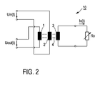
- Fig. 2 shows from another point of view the arrangement of the plural inductors 1 to 3 and possible connections of these inductors.
- the first inductor 1 forming the primary winding is supplied with an input voltage Uin(t) which will then cause a current flowing through the first inductor 1 and will further establish the magnetic field 4.
- the second inductor 2 with its inductive link to the first inductor 1 generates due to the induction principles an output voltage Uout(t) which will cause an output current if a corresponding circuitry is connected to the second inductor 2.
- an output voltage Uout(t) which will cause an output current if a corresponding circuitry is connected to the second inductor 2.
- the input voltage Uin(t) and the output voltage Uout(t) are time-variable physical parameters.
- the third inductor 3 (tertiary winding) is connected to a resistor Rv.
- This resistor Rv is provided in the form of a variable resistor the resistance value thereof can be varied within a predetermined range.
- a current Iv(t) is induced in the circuit composed of the third inductor 3 and the resistor Rv.
- the current Iv(t) (which is a time-variable physical parameter) flowing in this circuit is dependent upon the resistance value of the resistor Rv. That is, the value of the current Iv(t) through the third inductor 3 and the resistor Rv can be modified and, thus, adjusted by adjusting the resistance value of the resistor Rv.
- the circuit including the third inductor 3 and the (variable) resistor Rv constitutes an attenuator the function of which will be described in the following.
- the current Iv(t) is induced in the third inductor 3 due to the magnetic coupling to the first and second inductors 1 and 2. That is, the third inductor 3 collects at least a part of the electromagnetic field penetrating the first and second inductors 1 and 2. The at least part of the magnetic field 4 is transformed by the third inductor 3 into the current Iv(t) which is further dependent upon the resistance value of the resistance Rv.
- the current Iv(t) flowing through the resistor Rv generates heat in the resistor Rv so that the placement of the resistor in the current path of this circuit makes it possible to dissipate some power which is received by the magnetic coupling from the magnetic field 4 of the first and second inductors 1 and 2.
- the power dissipated in the resistor Rv due to the induced current Iv(t) in the circuit is equivalent to introduce losses inside the voltage transformer. That is, the dissipated power in the resistor Rv corresponds to voltage transformer losses.
- a predetermined power can be dissipated by the resistor Rv depending upon the magnetic field of the first and second inductors 1 and 2 and penetrating the third inductor 3.
- the resistor Rv is provided in the form of the variable resistor with an adjustable resistance value, this allows further influence on and control of the current Iv (t) flowing in the circuit of the third inductor 3 and the resistor Rv.
- the operation of the third inductor 3 corresponds to the attenuator of the voltage transformer. That is, when the (variable) resistor Rv is set to different resistance values within a predetermined range then different levels of power can be picked-up from the magnetic field 4 (magnetic flux ⁇ ) penetrating the third inductor 3 for dissipation by the resistor Rv, thereby attenuating the magnetic field 4 coupling all three inductors 1 to 3 to obtain the desired attenuation effect. Accordingly, the inductive link between the first and second inductors 1 and 2 (between the primary and secondary windings) can be adjusted by adjusting the resistance value of the (variable) resistor Rv connected across the terminals of the third inductor 3.
- the voltage transformer which is basically constituted by the first and second inductors 1 and 2 (primary and secondary windings) and at least one of the first and second inductors 1 and 2 is preferably made of spiral inductors placed close to each other, so that these two inductors 1 and 2 are substantially placed face to face.
- the first and second inductors 1 and 2 are arranged in a flat manner and may basically be disc-shaped.
- the third inductor 3 so that the first to third inductors 1 to 3 can be placed in close connection to each other to have a good magnetic coupling between these inductors.
- at least the first, second or third inductor 1 to 3 may be formed as spiral windings.
- the third inductor 3 being located closely related and preferably adjacent to the voltage transformer comprising the first and second inductors 1 and 2, an optimized influence on the magnetic field 4 penetrating the plurality of inductors 1 to 3 can be obtained, resulting in a variable attenuation of the magnetic field 4 depending upon the set resistance value of the (variable) resistor Rv connected to the third inductor 3.
- the third inductor 3 is arranged adjacent or proximate the voltage transformer, and specifically approximate to the second inductor 2 (secondary winding).
- the third inductor 3 can also be arranged between the first and second inductors 1 and 2 or can be arranged proximate to the first inductor (primary winding) 1 while ensuring the same attenuation effect as described above.
- an electromagnetic coupling is ensured and the variable attenuation of the magnetic coupling between the first and second inductors 1 and 2 is in a similar manner obtained by changing the resistance value of the resistor Rv.
- the first to third inductors 1 to 3 are made of spiral windings or inductors.
- the present invention is, however, not limited to such an arrangement, and the plurality of inductors 1 to 3 may also be provided in the form of inductors having a square shape or any other suitable flat shape which allows an arrangement of the plurality of inductors 1 to 3 close to each other for ensuring a suitable magnetic coupling.
- the windings of the first to third inductors may be provided in the form of discrete wires or may be arranged on the basis of technologies of semiconductors and printed boards (irrespective of whether the inductor assembly being arranged in a package or not).
- the windings of the inductors 1 to 3 are formed using semiconductor and/or printed board technologies.
- the inductor assembly 10 can be provided in a compact manner.
- a fourth inductor may be provided, located adjacent to one of the inductors 1 and 2 of the voltage transformer, the additional inductor (not shown in the Figures) also being connected to a resistor having a fixed resistance value or to a variable resistor the resistance value of which can be set depending upon predetermined conditions.
- the third inductor 3 has to be placed for optimize magnetic coupling close (close, adjacent) to the other inductors 1 to 3 so that the control concept according to the present invention can be obtained and the attenuation effect on the magnetic coupling as described above can be established preferably in conjunction with the variable resistor. Similar to the third inductor 3, the whole magnetic field 4 or at least a part thereof penetrates the fourth inductor.
- first to fourth inductors which may be formed based on semiconductor and/or printed board technologies, may further be arranged in different layers stacked according to a predetermined sequence. Furthermore, the third inductor 3 and said fourth inductor 4 may be arranged on different sides of the at least one of the first and second inductors 1 or 2.
- the solution according to the present invention for introducing a variable attenuator inside the above-described voltage transformer provides an efficient measure to obtain a specific influence on the magnetic field 4 of the voltage transformer and, thus, on the magnetic coupling between the first and second inductors 1 and 2 (primary and secondary windings of the voltage transformer) by means of the variable resistor Rv.
- This solution is highly effective in terms of noise and linearity in comparison to any arrangements using active components.
- the inductor assembly 10 and specifically the voltage transformer according to the present invention having introduced the variable attenuator inside the voltage transformer is applicable for frequencies allowing the use of preferably spiral inductors with reasonable sizes which can be made based on the semiconductor and/or printed board technologies.
- the attenuation function of the magnetic field 4 is obtained by dissipating some power of the inductor assembly in the third inductor, thereby introducing losses inside the voltage transformer in a controlled or controllable manner and weakening the magnetic field 4.
- the attenuation function can be set in a precise manner by directly varying the resistance value of the variable resistor Rv. Hence, the cooperation (functional connection by the magnetic field 4) of the primary and secondary inductors and specifically the magnetic coupling thereof can easily and precisely be adapted.
Landscapes
- Engineering & Computer Science (AREA)
- Power Engineering (AREA)
- Coils Or Transformers For Communication (AREA)
Abstract
Description
- The present invention refers to an inductor assembly, and more specifically to an inductor winding assembly of a transformer having a plurality of inductors.
- Reference
JP 06-290968 - According to the arrangement as disclosed in the above reference, besides the shielding effect between the primary and secondary coils it is difficult to obtain a controlled influence on the induction in the respective coils.
- It is therefore an object of the present invention to provide an inductor assembly which allows adjustment of an inductive link between predetermined inductors.
- According to the present invention, this object is accomplished by a winding assembly as put forward in the appended claims.
- The inductor assembly of a transformer according to the present invention comprises a first inductor, a second inductor being magnetically coupled to the first inductor, and a third inductor being magnetically coupled to the first and second inductors, wherein the third inductor being connected to a variable resistor adapted for adjusting the magnetic coupling between the first and the second inductors by varying a resistance value of the variable resistor.
- Hence, according to the present invention, the inductor assembly of the transformer including the first (primary) inductor and the second (secondary) inductor includes the third (tertiary) inductor which allows a specific operation thereof in that the magnetic coupling between the primary inductor and the secondary inductor can be influenced by means of the third inductor. This is specifically performed by modifying the resistance value of a variable resistor which is connected to the third inductor. The third inductor in conjunction with the variable resistor constitutes a variable attenuator inside the transformer (voltage transformer) having the inductor assembly. The attenuation function is obtained by dissipating some power of the inductor assembly in the third inductor, thereby introducing losses inside the voltage transformer. The attenuation function can be obtained and can be set in a precise manner by directly varying the resistance value of the variable resistor. Hence, the cooperation of the primary and secondary inductors and specifically the magnetic coupling thereof can easily be adapted.
- Preferred embodiments of the present invention are defined in the dependent claims.
- The at least the first, second or third inductor may be formed as spiral windings. The first inductor and the second inductor form a transformer.
- The third inductor may be arranged adj acent to at least one of the first and second inductors, and at least one of the first to third inductors may be formed by using semiconductor and/or printed board technologies.
- The variable resistor may be adapted for adjusting the magnetic coupling by adjusting a current induced in the third inductor.
- The induced current may cause a power dissipation in the variable resistor, the variable resistor and the third inductor constituting an attenuator of the magnetic coupling between the first and second inductors.
- The inductor assembly may further include a fourth inductor being magnetically coupled to the at least first and second inductors, and the fourth inductor being connected to a further variable resistor adapted for adjusting the magnetic coupling between at least the first and the second inductors by varying a resistance value of the further variable resistor.
- The first to fourth inductors may be flat disc-shaped windings.
- The fourth inductor may be arranged adjacent to at least one of the first and second inductors, the third inductor and the fourth inductor being arranged on different sides of the at least one of the first and second inductors.
- The third inductor being magnetically coupled to the first and second inductors by at least a part of the magnetic field generated by the first inductor.
- The fourth inductor may be magnetically coupled to the first and second inductors by at least a part of the magnetic field generated by the first inductor.
- The fourth inductor may be provided in the form of spiral windings.
- The first to fourth inductors may be formed based on semiconductor and/or printed board technologies, and may be arranged in different layers stacked according to a predetermined sequence.
- The present invention is further elucidated by the following Figures and examples, which are not intended to limit the scope of the invention. The person skilled in the art will understand that various embodiments may be combined.
- These and other aspects of the invention will be apparent from and elucidated with reference to the embodiments described hereinafter. In the following drawings,
-
Fig. 1 shows a schematic overview of the inductor assembly according to the present invention, and -
Fig. 2 shows the basic circuitry in conjunction with the inductor assembly according to the present invention. - According to the basic arrangement shown in
Fig. 1 , aninductor assembly 10 of a transformer (voltage transformer) includes a first inductor 1 which constitutes the primary winding or primary coil. Asecond inductor 2 is provided in close spatial relationship to the first inductor 1 and constitutes the secondary winding or secondary coil of the transformer. In addition to the first andsecond inductors 1 and 2, a third inductor 3 is arranged also in close spatial relationship to the first andsecond inductors 1 and 2. - The arrangement of the first to third inductors (primary to tertiary windings or coils) constitutes the
inductor assembly 10 wherein each of the first to third inductors 1 to 3 is coupled basically to a common magnetic field 4. The common magnetic field 4 as shown inFig. 1 and further indicated by Φ representing magnetic flux, penetrates each of the first to third inductors 1 to 3 and therefore provides a magnetic coupling of each of the plurality of inductors 1 to 3 with the respective other inductors. - Accordingly, due to the magnetic coupling of the first inductor 1 to the
second inductor 2, a voltage applied to the first inductor 1 will cause a corresponding current and will further cause, via the magnetic field (magnetic flux Φ ) an induction voltage in the second inductor 2 (secondary winding). In case thesecond inductor 2 is connected to any circuitry at its terminals (forming a load to the second inductor 2), a corresponding current will flow to the circuitry connected thereto. - As mentioned above and as depicted in
Fig. 1 the first and second inductors (primary and secondary windings) 1 and 2 have an inductive link, i.e. are linked by the magnetic field 4 represented inFig. 1 by the magnetic flux Φ. This allows in a corresponding manner the transmission of power from the first inductor 1 to thesecond inductor 2, and in a corresponding manner from the primary winding to the secondary winding of the transformer. - As is further depicted in
Fig. 1 , also the third inductor 3 (tertiary winding or coil) is arranged in such a manner relative to the first andsecond inductors 1 and 2, that the magnetic field basically driven by the first inductor 1 (primary winding) also penetrates the third inductor 3. Hence, also the third inductor 3 is magnetically coupled to the first andsecond inductors 1 and 2 so that the same magnetic field (basically derived from the first inductor 1) provides a magnetic coupling of all of the plurality of inductors 1 to 3. That is, all three inductors 1 to 3 are magnetically coupled by the same magnetic field 4 ( Φ ) according to the principles of magnetic induction, and specifically the third inductor 3 may be arranged adjacent to at least one of the first andsecond inductors 1 and 2. -
Fig. 2 shows from another point of view the arrangement of the plural inductors 1 to 3 and possible connections of these inductors. The first inductor 1 forming the primary winding is supplied with an input voltage Uin(t) which will then cause a current flowing through the first inductor 1 and will further establish the magnetic field 4. - The
second inductor 2 with its inductive link to the first inductor 1 generates due to the induction principles an output voltage Uout(t) which will cause an output current if a corresponding circuitry is connected to thesecond inductor 2. According to the regular principles of a transformer power can be transmitted from the primary side (inductor 1) to the secondary side (inductor 2). The input voltage Uin(t) and the output voltage Uout(t) are time-variable physical parameters. - As is also depicted in
Fig. 1 , the third inductor 3 (tertiary winding) is connected to a resistor Rv. This resistor Rv is provided in the form of a variable resistor the resistance value thereof can be varied within a predetermined range. - Based on the induction principles a current Iv(t) is induced in the circuit composed of the third inductor 3 and the resistor Rv. The current Iv(t) (which is a time-variable physical parameter) flowing in this circuit is dependent upon the resistance value of the resistor Rv. That is, the value of the current Iv(t) through the third inductor 3 and the resistor Rv can be modified and, thus, adjusted by adjusting the resistance value of the resistor Rv. The circuit including the third inductor 3 and the (variable) resistor Rv constitutes an attenuator the function of which will be described in the following.
- The current Iv(t) is induced in the third inductor 3 due to the magnetic coupling to the first and
second inductors 1 and 2. That is, the third inductor 3 collects at least a part of the electromagnetic field penetrating the first andsecond inductors 1 and 2. The at least part of the magnetic field 4 is transformed by the third inductor 3 into the current Iv(t) which is further dependent upon the resistance value of the resistance Rv. The current Iv(t) flowing through the resistor Rv generates heat in the resistor Rv so that the placement of the resistor in the current path of this circuit makes it possible to dissipate some power which is received by the magnetic coupling from the magnetic field 4 of the first andsecond inductors 1 and 2. The power dissipated in the resistor Rv due to the induced current Iv(t) in the circuit is equivalent to introduce losses inside the voltage transformer. That is, the dissipated power in the resistor Rv corresponds to voltage transformer losses. - In case a fixed resistance value of the resistor Rv is established, a predetermined power can be dissipated by the resistor Rv depending upon the magnetic field of the first and
second inductors 1 and 2 and penetrating the third inductor 3. In case the resistor Rv is provided in the form of the variable resistor with an adjustable resistance value, this allows further influence on and control of the current Iv (t) flowing in the circuit of the third inductor 3 and the resistor Rv. - When picking up power supplied to the third inductor 3 by means of the magnetic coupling (magnetic field 4) the operation of the third inductor 3 corresponds to the attenuator of the voltage transformer. That is, when the (variable) resistor Rv is set to different resistance values within a predetermined range then different levels of power can be picked-up from the magnetic field 4 (magnetic flux Φ) penetrating the third inductor 3 for dissipation by the resistor Rv, thereby attenuating the magnetic field 4 coupling all three inductors 1 to 3 to obtain the desired attenuation effect. Accordingly, the inductive link between the first and second inductors 1 and 2 (between the primary and secondary windings) can be adjusted by adjusting the resistance value of the (variable) resistor Rv connected across the terminals of the third inductor 3.
- Regarding the arrangement of the plurality of inductors 1 to 3, the voltage transformer which is basically constituted by the first and second inductors 1 and 2 (primary and secondary windings) and at least one of the first and
second inductors 1 and 2 is preferably made of spiral inductors placed close to each other, so that these twoinductors 1 and 2 are substantially placed face to face. Preferably, at least the first andsecond inductors 1 and 2 are arranged in a flat manner and may basically be disc-shaped. This also holds for the third inductor 3, so that the first to third inductors 1 to 3 can be placed in close connection to each other to have a good magnetic coupling between these inductors. Basically, at least the first, second or third inductor 1 to 3 may be formed as spiral windings. - With the third inductor 3 being located closely related and preferably adjacent to the voltage transformer comprising the first and
second inductors 1 and 2, an optimized influence on the magnetic field 4 penetrating the plurality of inductors 1 to 3 can be obtained, resulting in a variable attenuation of the magnetic field 4 depending upon the set resistance value of the (variable) resistor Rv connected to the third inductor 3. - It is mentioned above that the third inductor 3 is arranged adjacent or proximate the voltage transformer, and specifically approximate to the second inductor 2 (secondary winding).
- According to a further embodiment of the present invention, the third inductor 3 can also be arranged between the first and
second inductors 1 and 2 or can be arranged proximate to the first inductor (primary winding) 1 while ensuring the same attenuation effect as described above. In both further cases and alternatively to the specific arrangement shown inFig. 1 , an electromagnetic coupling is ensured and the variable attenuation of the magnetic coupling between the first andsecond inductors 1 and 2 is in a similar manner obtained by changing the resistance value of the resistor Rv. - According to the embodiment the first to third inductors 1 to 3 are made of spiral windings or inductors. The present invention is, however, not limited to such an arrangement, and the plurality of inductors 1 to 3 may also be provided in the form of inductors having a square shape or any other suitable flat shape which allows an arrangement of the plurality of inductors 1 to 3 close to each other for ensuring a suitable magnetic coupling.
- The windings of the first to third inductors may be provided in the form of discrete wires or may be arranged on the basis of technologies of semiconductors and printed boards (irrespective of whether the inductor assembly being arranged in a package or not). Preferably, the windings of the inductors 1 to 3 are formed using semiconductor and/or printed board technologies. The
inductor assembly 10 can be provided in a compact manner. - According to a further alternative embodiment, in addition to the inductor arrangement (inductor assembly) shown in
Fig. 1 , a fourth inductor may be provided, located adjacent to one of theinductors 1 and 2 of the voltage transformer, the additional inductor (not shown in the Figures) also being connected to a resistor having a fixed resistance value or to a variable resistor the resistance value of which can be set depending upon predetermined conditions. - In the arrangement of plural inductors including the fourth inductor in a corresponding manner as a third inductor 3, the third inductor 3 has to be placed for optimize magnetic coupling close (close, adjacent) to the other inductors 1 to 3 so that the control concept according to the present invention can be obtained and the attenuation effect on the magnetic coupling as described above can be established preferably in conjunction with the variable resistor. Similar to the third inductor 3, the whole magnetic field 4 or at least a part thereof penetrates the fourth inductor.
- Moreover, the first to fourth inductors which may be formed based on semiconductor and/or printed board technologies, may further be arranged in different layers stacked according to a predetermined sequence. Furthermore, the third inductor 3 and said fourth inductor 4 may be arranged on different sides of the at least one of the first and
second inductors 1 or 2. - The solution according to the present invention for introducing a variable attenuator inside the above-described voltage transformer (first and second inductors 1 and 2) provides an efficient measure to obtain a specific influence on the magnetic field 4 of the voltage transformer and, thus, on the magnetic coupling between the first and second inductors 1 and 2 (primary and secondary windings of the voltage transformer) by means of the variable resistor Rv. This solution is highly effective in terms of noise and linearity in comparison to any arrangements using active components. The
inductor assembly 10 and specifically the voltage transformer according to the present invention having introduced the variable attenuator inside the voltage transformer is applicable for frequencies allowing the use of preferably spiral inductors with reasonable sizes which can be made based on the semiconductor and/or printed board technologies. - The attenuation function of the magnetic field 4 is obtained by dissipating some power of the inductor assembly in the third inductor, thereby introducing losses inside the voltage transformer in a controlled or controllable manner and weakening the magnetic field 4. The attenuation function can be set in a precise manner by directly varying the resistance value of the variable resistor Rv. Hence, the cooperation (functional connection by the magnetic field 4) of the primary and secondary inductors and specifically the magnetic coupling thereof can easily and precisely be adapted.
- While the invention has been illustrated and described in detail in the drawings and foregoing description, such illustration and description are to be considered illustrative or exemplary and not restrictive; the invention is not limited to the disclosed embodiments.
- Other variations to the disclosed embodiments can be understood and effected by those skilled in the art in practicing the claimed invention, from a study of the drawings, the disclosure, and the appended claims.
- In the claims, the word "comprising" does not exclude other elements or steps, and the indefinite article "a" or "an" does not exclude a plurality. Any reference signs in the claims should not be construed as limiting the scope.
Claims (14)
- Inductor assembly (10) of a transformer, comprising:- a first inductor (1),- a second inductor (2) being magnetically coupled to the first inductor, and- a third inductor (3) being magnetically coupled to said first and second inductors,wherein- said third inductor being connected to a variable resistor (Rv) adapted for adjusting the magnetic coupling between the first and the second inductors by varying a resistance value of said variable resistor.
- Inductor assembly according to claim 1, wherein at least the first, second or third inductors (1, 2, 3) being formed as spiral windings.
- Inductor assembly according to claim 1, wherein said first inductor (1) and said second inductor (2) constitute a transformer.
- Inductor assembly according to claim 1, wherein said third inductor (3) being arranged adjacent to at least one of the first and second inductors (1, 2).
- Inductor assembly according to claim 1, wherein at least one of said first to third inductors (1, 2, 3) being formed by using semiconductor and/or printed board technologies.
- Inductor assembly according to claim 1, wherein said variable resistor (Rv) being adapted for adjusting the magnetic coupling by adjusting a current (Iv(t)) induced in said third inductor (3).
- Inductor assembly according to claim 6, wherein said induced current (Iv(t)) causes a power dissipation in said variable resistor (Rv), said variable resistor and said third inductor (3) constituting an attenuator of the magnetic coupling between said first and second inductors (1, 2).
- Inductor assembly according to claim 1, further including a fourth inductor being magnetically coupled to said at least first and second inductors (1, 2), and said fourth inductor being connected to a further variable resistor adapted for adjusting the magnetic coupling between the first and said second inductors by varying a resistance value of said further variable resistor.
- Inductor assembly according to claim 8, wherein said first to fourth inductors are flat disc-shaped windings.
- Inductor assembly according to claim 8, wherein said fourth inductor being arranged adjacent to at least one of the first and second inductors (1, 2), said third inductor (3) and said fourth inductor (4) being arranged on different sides of the at least one of the first and second inductors.
- Inductor assembly according to one of claims 1 to 7, wherein said third inductor (3) being magnetically coupled to said first and second inductors (1, 2) by at least a part of said magnetic field (4) generated by said first inductor.
- Inductor assembly according to one of claims 8 to 10, wherein said fourth inductor being magnetically coupled to said first and second inductors (1, 2) by at least a part of said magnetic field (4) generated by said first inductor.
- Inductor assembly according to claim 8, wherein said fourth inductor is provided in the form of spiral windings.
- Inductor assembly according to claim 8, wherein said first to fourth inductors (1, 2, 3, 4) are formed based on semiconductor and/or printed board technologies, and being arranged in different layers stacked according to a predetermined sequence.
Priority Applications (1)
| Application Number | Priority Date | Filing Date | Title |
|---|---|---|---|
| EP09305711A EP2151834A3 (en) | 2008-08-05 | 2009-07-29 | Inductor assembly |
Applications Claiming Priority (2)
| Application Number | Priority Date | Filing Date | Title |
|---|---|---|---|
| EP08290751 | 2008-08-05 | ||
| EP09305711A EP2151834A3 (en) | 2008-08-05 | 2009-07-29 | Inductor assembly |
Publications (2)
| Publication Number | Publication Date |
|---|---|
| EP2151834A2 true EP2151834A2 (en) | 2010-02-10 |
| EP2151834A3 EP2151834A3 (en) | 2012-09-19 |
Family
ID=41308409
Family Applications (1)
| Application Number | Title | Priority Date | Filing Date |
|---|---|---|---|
| EP09305711A Withdrawn EP2151834A3 (en) | 2008-08-05 | 2009-07-29 | Inductor assembly |
Country Status (2)
| Country | Link |
|---|---|
| US (1) | US8203417B2 (en) |
| EP (1) | EP2151834A3 (en) |
Families Citing this family (9)
| Publication number | Priority date | Publication date | Assignee | Title |
|---|---|---|---|---|
| DE112012003966B4 (en) * | 2011-09-23 | 2024-01-11 | Tensorcom, Inc. | High performance divider with pilot control, clock amplification and series equalizer coils |
| US8487695B2 (en) | 2011-09-23 | 2013-07-16 | Tensorcom, Inc. | Differential source follower having 6dB gain with applications to WiGig baseband filters |
| US8406710B1 (en) | 2011-09-23 | 2013-03-26 | Tensorcom, Inc. | Method and apparatus of minimizing extrinsic parasitic resistance in 60 GHz power amplifier circuits |
| US8680899B2 (en) | 2011-09-23 | 2014-03-25 | Tensorcom, Inc. | High performance divider using feed forward, clock amplification and series peaking inductors |
| US10115661B2 (en) | 2013-02-08 | 2018-10-30 | Qualcomm Incorporated | Substrate-less discrete coupled inductor structure |
| KR102642071B1 (en) | 2015-11-17 | 2024-02-28 | 텐서컴, 인코퍼레이티드 | Highly linear WiGig baseband amplifier with channel selection filter |
| WO2018208990A1 (en) * | 2017-05-09 | 2018-11-15 | The Regents Of The University Of California | Systems and methods for low-power near-field-communication |
| WO2019036519A1 (en) | 2017-08-14 | 2019-02-21 | The Regents Of The University Of California | Load-induced resonance-shift-keying modulation scheme for simultaneous near-field wireless power and data transmission through a pair of inductive coils |
| US10976381B2 (en) * | 2019-05-10 | 2021-04-13 | Mis Security, Llc | Magnetic field monitor having automated quantitative calibration of magnetic field sensor |
Citations (1)
| Publication number | Priority date | Publication date | Assignee | Title |
|---|---|---|---|---|
| JPH06290968A (en) | 1993-03-31 | 1994-10-18 | Yokogawa Electric Corp | Printed coil transformer |
Family Cites Families (10)
| Publication number | Priority date | Publication date | Assignee | Title |
|---|---|---|---|---|
| FR833105A (en) * | 1937-02-05 | 1938-10-12 | Loewe Opta Gmbh | Transformer coupling system for use in devices sensitive to magnetic stray fields |
| US4873757A (en) * | 1987-07-08 | 1989-10-17 | The Foxboro Company | Method of making a multilayer electrical coil |
| DE69306754T2 (en) * | 1993-04-21 | 1997-07-10 | Thomson Tubes & Displays S.A., Paris | Flexible additional deflection coil |
| US5610433A (en) * | 1995-03-13 | 1997-03-11 | National Semiconductor Corporation | Multi-turn, multi-level IC inductor with crossovers |
| US5600293A (en) * | 1994-06-14 | 1997-02-04 | The United States Of America As Represented By The Secretary Of The Army | Integrated magnetic exploding foil initiator fire set |
| US6885275B1 (en) * | 1998-11-12 | 2005-04-26 | Broadcom Corporation | Multi-track integrated spiral inductor |
| US6479976B1 (en) * | 2001-06-28 | 2002-11-12 | Thomas G. Edel | Method and apparatus for accurate measurement of pulsed electric currents utilizing ordinary current transformers |
| KR100420948B1 (en) * | 2001-08-22 | 2004-03-02 | 한국전자통신연구원 | Spiral inductor having parallel-branch structure |
| US7486167B2 (en) * | 2005-08-24 | 2009-02-03 | Avago Technologies General Ip (Singapore) Pte. Ltd. | Cross-coupled inductor pair formed in an integrated circuit |
| US7667440B2 (en) * | 2007-01-05 | 2010-02-23 | Intersil Americas Inc. | Power-supply control |
-
2009
- 2009-07-29 EP EP09305711A patent/EP2151834A3/en not_active Withdrawn
- 2009-08-05 US US12/536,037 patent/US8203417B2/en not_active Expired - Fee Related
Patent Citations (1)
| Publication number | Priority date | Publication date | Assignee | Title |
|---|---|---|---|---|
| JPH06290968A (en) | 1993-03-31 | 1994-10-18 | Yokogawa Electric Corp | Printed coil transformer |
Also Published As
| Publication number | Publication date |
|---|---|
| EP2151834A3 (en) | 2012-09-19 |
| US8203417B2 (en) | 2012-06-19 |
| US20100039092A1 (en) | 2010-02-18 |
Similar Documents
| Publication | Publication Date | Title |
|---|---|---|
| EP2151834A2 (en) | Inductor assembly | |
| US6222437B1 (en) | Surface mounted magnetic components having sheet material windings and a power supply including such components | |
| KR100625785B1 (en) | Step up transformer for driving magnetron and transformer for power supply for magnetron driving | |
| CN105518810B (en) | Integrated magnet assembly and its assemble method | |
| CN101661825B (en) | Magnetics for Power Converters | |
| RU2662798C2 (en) | Linear electromagnetic device | |
| CN111587466B (en) | power converter | |
| US10930422B2 (en) | Power electronics device with improved isolation performance | |
| JP5939274B2 (en) | Power supply | |
| EP2933803A1 (en) | Magnetic element with multiple air gaps | |
| CN113950727A (en) | Stacked matrix transformer | |
| WO2018126155A1 (en) | Leadframe inductor | |
| US9837923B2 (en) | Integrated power converter and transformer | |
| US12159744B2 (en) | Inductor with variable permeability core | |
| TW201011790A (en) | Transformer for reducing EMI and power conversion circuit using the same | |
| US20180218820A1 (en) | Magnetic core signal modulation | |
| KR101131586B1 (en) | Resonator for magnetic resonance power transmission device using current source input | |
| US12347789B2 (en) | Air-core transformer package with ferrite electro-magnetic interference (EMI) shielding of integrated-circuit (IC) chip | |
| Zhang et al. | In-board magnetics processes | |
| EP0896419A2 (en) | Power converter incorporated in a magnetic circuit | |
| US12131864B2 (en) | Transformer with integral inductor | |
| JP2019030124A (en) | Circulating current reduction circuit, transformer unit | |
| JP6823130B2 (en) | Filter device | |
| KR102075955B1 (en) | Two-in-one planer inductor | |
| CN118197756A (en) | Damping inductor, filter device and compressor device |
Legal Events
| Date | Code | Title | Description |
|---|---|---|---|
| PUAI | Public reference made under article 153(3) epc to a published international application that has entered the european phase |
Free format text: ORIGINAL CODE: 0009012 |
|
| AK | Designated contracting states |
Kind code of ref document: A2 Designated state(s): AT BE BG CH CY CZ DE DK EE ES FI FR GB GR HR HU IE IS IT LI LT LU LV MC MK MT NL NO PL PT RO SE SI SK SM TR |
|
| AX | Request for extension of the european patent |
Extension state: AL BA RS |
|
| PUAL | Search report despatched |
Free format text: ORIGINAL CODE: 0009013 |
|
| AK | Designated contracting states |
Kind code of ref document: A3 Designated state(s): AT BE BG CH CY CZ DE DK EE ES FI FR GB GR HR HU IE IS IT LI LT LU LV MC MK MT NL NO PL PT RO SE SI SK SM TR |
|
| AX | Request for extension of the european patent |
Extension state: AL BA RS |
|
| RIC1 | Information provided on ipc code assigned before grant |
Ipc: H01F 27/38 20060101AFI20120814BHEP |
|
| STAA | Information on the status of an ep patent application or granted ep patent |
Free format text: STATUS: THE APPLICATION IS DEEMED TO BE WITHDRAWN |
|
| 18D | Application deemed to be withdrawn |
Effective date: 20130320 |