EP2151047B1 - Linear rf amplifier with polar feedback - Google Patents
Linear rf amplifier with polar feedback Download PDFInfo
- Publication number
- EP2151047B1 EP2151047B1 EP08754245.2A EP08754245A EP2151047B1 EP 2151047 B1 EP2151047 B1 EP 2151047B1 EP 08754245 A EP08754245 A EP 08754245A EP 2151047 B1 EP2151047 B1 EP 2151047B1
- Authority
- EP
- European Patent Office
- Prior art keywords
- signal
- amplitude
- feedback
- phase
- modulator
- Prior art date
- Legal status (The legal status is an assumption and is not a legal conclusion. Google has not performed a legal analysis and makes no representation as to the accuracy of the status listed.)
- Active
Links
Images







Classifications
-
- H—ELECTRICITY
- H03—ELECTRONIC CIRCUITRY
- H03F—AMPLIFIERS
- H03F1/00—Details of amplifiers with only discharge tubes, only semiconductor devices or only unspecified devices as amplifying elements
- H03F1/32—Modifications of amplifiers to reduce non-linear distortion
- H03F1/3241—Modifications of amplifiers to reduce non-linear distortion using predistortion circuits
- H03F1/3282—Acting on the phase and the amplitude of the input signal
-
- H—ELECTRICITY
- H03—ELECTRONIC CIRCUITRY
- H03F—AMPLIFIERS
- H03F1/00—Details of amplifiers with only discharge tubes, only semiconductor devices or only unspecified devices as amplifying elements
- H03F1/02—Modifications of amplifiers to raise the efficiency, e.g. gliding Class A stages, use of an auxiliary oscillation
- H03F1/04—Modifications of amplifiers to raise the efficiency, e.g. gliding Class A stages, use of an auxiliary oscillation in discharge-tube amplifiers
- H03F1/06—Modifications of amplifiers to raise the efficiency, e.g. gliding Class A stages, use of an auxiliary oscillation in discharge-tube amplifiers to raise the efficiency of amplifying modulated radio frequency waves; to raise the efficiency of amplifiers acting also as modulators
-
- H—ELECTRICITY
- H03—ELECTRONIC CIRCUITRY
- H03C—MODULATION
- H03C5/00—Amplitude modulation and angle modulation produced simultaneously or at will by the same modulating signal
-
- H—ELECTRICITY
- H03—ELECTRONIC CIRCUITRY
- H03F—AMPLIFIERS
- H03F1/00—Details of amplifiers with only discharge tubes, only semiconductor devices or only unspecified devices as amplifying elements
- H03F1/02—Modifications of amplifiers to raise the efficiency, e.g. gliding Class A stages, use of an auxiliary oscillation
- H03F1/0205—Modifications of amplifiers to raise the efficiency, e.g. gliding Class A stages, use of an auxiliary oscillation in transistor amplifiers
-
- H—ELECTRICITY
- H03—ELECTRONIC CIRCUITRY
- H03F—AMPLIFIERS
- H03F1/00—Details of amplifiers with only discharge tubes, only semiconductor devices or only unspecified devices as amplifying elements
- H03F1/32—Modifications of amplifiers to reduce non-linear distortion
-
- H—ELECTRICITY
- H03—ELECTRONIC CIRCUITRY
- H03F—AMPLIFIERS
- H03F1/00—Details of amplifiers with only discharge tubes, only semiconductor devices or only unspecified devices as amplifying elements
- H03F1/32—Modifications of amplifiers to reduce non-linear distortion
- H03F1/3241—Modifications of amplifiers to reduce non-linear distortion using predistortion circuits
- H03F1/3247—Modifications of amplifiers to reduce non-linear distortion using predistortion circuits using feedback acting on predistortion circuits
-
- H—ELECTRICITY
- H03—ELECTRONIC CIRCUITRY
- H03F—AMPLIFIERS
- H03F1/00—Details of amplifiers with only discharge tubes, only semiconductor devices or only unspecified devices as amplifying elements
- H03F1/32—Modifications of amplifiers to reduce non-linear distortion
- H03F1/3241—Modifications of amplifiers to reduce non-linear distortion using predistortion circuits
- H03F1/3294—Acting on the real and imaginary components of the input signal
-
- H—ELECTRICITY
- H03—ELECTRONIC CIRCUITRY
- H03F—AMPLIFIERS
- H03F3/00—Amplifiers with only discharge tubes or only semiconductor devices as amplifying elements
- H03F3/189—High-frequency amplifiers, e.g. radio frequency amplifiers
-
- H—ELECTRICITY
- H03—ELECTRONIC CIRCUITRY
- H03F—AMPLIFIERS
- H03F3/00—Amplifiers with only discharge tubes or only semiconductor devices as amplifying elements
- H03F3/20—Power amplifiers, e.g. Class B amplifiers, Class C amplifiers
- H03F3/24—Power amplifiers, e.g. Class B amplifiers, Class C amplifiers of transmitter output stages
-
- H—ELECTRICITY
- H04—ELECTRIC COMMUNICATION TECHNIQUE
- H04B—TRANSMISSION
- H04B1/00—Details of transmission systems, not covered by a single one of groups H04B3/00 - H04B13/00; Details of transmission systems not characterised by the medium used for transmission
- H04B1/02—Transmitters
- H04B1/04—Circuits
- H04B1/0475—Circuits with means for limiting noise, interference or distortion
-
- H—ELECTRICITY
- H04—ELECTRIC COMMUNICATION TECHNIQUE
- H04L—TRANSMISSION OF DIGITAL INFORMATION, e.g. TELEGRAPHIC COMMUNICATION
- H04L27/00—Modulated-carrier systems
- H04L27/32—Carrier systems characterised by combinations of two or more of the types covered by groups H04L27/02, H04L27/10, H04L27/18 or H04L27/26
- H04L27/34—Amplitude- and phase-modulated carrier systems, e.g. quadrature-amplitude modulated carrier systems
- H04L27/36—Modulator circuits; Transmitter circuits
- H04L27/362—Modulation using more than one carrier, e.g. with quadrature carriers, separately amplitude modulated
- H04L27/364—Arrangements for overcoming imperfections in the modulator, e.g. quadrature error or unbalanced I and Q levels
-
- H—ELECTRICITY
- H04—ELECTRIC COMMUNICATION TECHNIQUE
- H04L—TRANSMISSION OF DIGITAL INFORMATION, e.g. TELEGRAPHIC COMMUNICATION
- H04L27/00—Modulated-carrier systems
- H04L27/32—Carrier systems characterised by combinations of two or more of the types covered by groups H04L27/02, H04L27/10, H04L27/18 or H04L27/26
- H04L27/34—Amplitude- and phase-modulated carrier systems, e.g. quadrature-amplitude modulated carrier systems
- H04L27/36—Modulator circuits; Transmitter circuits
- H04L27/366—Arrangements for compensating undesirable properties of the transmission path between the modulator and the demodulator
- H04L27/367—Arrangements for compensating undesirable properties of the transmission path between the modulator and the demodulator using predistortion
- H04L27/368—Arrangements for compensating undesirable properties of the transmission path between the modulator and the demodulator using predistortion adaptive predistortion
-
- H—ELECTRICITY
- H03—ELECTRONIC CIRCUITRY
- H03F—AMPLIFIERS
- H03F2200/00—Indexing scheme relating to amplifiers
- H03F2200/321—Use of a microprocessor in an amplifier circuit or its control circuit
-
- H—ELECTRICITY
- H03—ELECTRONIC CIRCUITRY
- H03F—AMPLIFIERS
- H03F2200/00—Indexing scheme relating to amplifiers
- H03F2200/324—An amplitude modulator or demodulator being used in the amplifier circuit
-
- H—ELECTRICITY
- H03—ELECTRONIC CIRCUITRY
- H03F—AMPLIFIERS
- H03F2200/00—Indexing scheme relating to amplifiers
- H03F2200/333—A frequency modulator or demodulator being used in the amplifier circuit
-
- H—ELECTRICITY
- H03—ELECTRONIC CIRCUITRY
- H03F—AMPLIFIERS
- H03F2200/00—Indexing scheme relating to amplifiers
- H03F2200/336—A I/Q, i.e. phase quadrature, modulator or demodulator being used in an amplifying circuit
-
- H—ELECTRICITY
- H03—ELECTRONIC CIRCUITRY
- H03F—AMPLIFIERS
- H03F2200/00—Indexing scheme relating to amplifiers
- H03F2200/393—A measuring circuit being coupled to the output of an amplifier
-
- H—ELECTRICITY
- H03—ELECTRONIC CIRCUITRY
- H03F—AMPLIFIERS
- H03F2200/00—Indexing scheme relating to amplifiers
- H03F2200/451—Indexing scheme relating to amplifiers the amplifier being a radio frequency amplifier
-
- H—ELECTRICITY
- H03—ELECTRONIC CIRCUITRY
- H03F—AMPLIFIERS
- H03F2200/00—Indexing scheme relating to amplifiers
- H03F2200/78—A comparator being used in a controlling circuit of an amplifier
Definitions
- the invention relates generally to systems for linear amplification of radio-frequency (RF) signals and, more particularly, to systems for linear amplification of RF signals using polar feedback.
- RF radio-frequency
- RF radio-frequency
- an RF carrier wave may be modulated with a baseband signal containing information to be communicated.
- the modulated RF signal may then be amplified and transmitted.
- a certain degree of care must be taken in the amplification of the RF signal to ensure that it is not distorted. If the RF transmission is distorted, a receiver may not be able to properly demodulate the RF signal and recover the original baseband signal.
- the amplification process must remain relatively linear.
- One way of accomplishing this is to use a highly backed-off amplifier (i.e., an amplifier operated well below its maximum power capacity). By backing off the amplifier, it may be operated in a relatively linear fashion. However, amplifiers typically operate very inefficiently when backed off far from their maximum capacity.
- the RF signal may be converted to baseband (i.e., a low-frequency signal, similar to audio frequencies) at which high gain may be obtained.
- the highly amplified baseband signal may then be converted back to RF and applied to the input of an RF amplifier. This process requires demodulating the signal from RF to baseband and then modulating the amplified baseband signal back to RF.
- Cartesian feedback system In a Cartesian feedback system, the demodulation process produces "in-phase” and “quadrature,” or “IQ” signals. Cartesian feedback system are sensitive to operating conditions such as temperature and require IQ demodulators and modulators with very tightly controlled phase characteristics. To control the phase characteristics properly, Cartesian feedback requires a complex auxiliary control system that is difficult to implement and adjust. In addition, systems employing Cartesian feedback typically are expensive and complex. As a result, Cartesian feedback is not desirable for certain types of RF applications, such as two-way radio communication.
- United States Patent Application 2007/0037530 discloses a system in which power amplifier feedback is routed to the power control port of the power amplifier to complete a feedback mechanism.
- European Patent Application Publication EP 1 011 192 A2 teaches where feedback from a power amplifier is routed to gain and phase error detectors and the detected gain and phase errors are routed to an adaptive predistorter which provides correction signals to amplitude and phase modulators, thus providing a closed-loop feedback system.
- United States Patent 6,043,707 teaches a system with feedback from a power amplifier comprising an IQ modulator configured to modulate an RF carrier signal based on a pair of IQ signals representative of at least the phase component of an original waveform, a fixed phase shifter in communication with the IQ modulator; a feedback-controlled amplitude modulator in communication with the power amplifier, an amplitude detector comprising an IQ demodulator in communication with the power amplifier and the fixed phase shifter, wherein a feedback network is configured to generate a feedback control signal.
- International Patent Application Publication WO 00/72438 discloses IQ modulation in the forward path in the context of a system with a feedback path from a power amplifier.
- the solution is provided by a system for power amplification of an RF signal as defined in claim 1.
- the system includes a feedback-controlled modulator configured to modulate an RF signal based on a feedback-corrected control signal.
- the modulator is further configured to generate a modulated RF signal.
- the system further includes a power amplifier in communication with the modulator.
- the amplifier is configured to amplify the modulated RF signal and to generate an amplified RF output signal.
- the system also includes an amplitude detector in communication with the power amplifier.
- the amplitude detector is configured to detect an amplitude characteristic of the amplified RF output signal and to generate an amplitude feedback signal.
- the system includes a feedback network in communication with the amplitude detector and the modulator.
- the feedback network is configured to generate a feedback-corrected control signal based on the difference between the amplitude feedback signal and an amplitude component of the original waveform.
- Embodiments of the invention include systems for power amplification of an RF signal, including amplifiers, transmitters, etc.
- the embodiments described in this application may be implemented in a wide range of applications, such as, for example, two-way radios, simulcast communication systems, and mobile telephones.
- FIG. 1 is a block diagram illustrating a system 100 for linear amplification using polar amplitude feedback.
- Polar amplitude feedback is provided based on the magnitude channel of a polar feedback network.
- the system 100 modulates and amplifies an RF signal 102 to generate an output signal 104.
- the modulation is provided by an amplitude modulator 110, and the amplification is provided by a power amplifier 112.
- the amplitude modulator 110 and the power amplifier 112 may take any suitable form, depending on the particular application. For example, the modulation and amplification functions may be combined into a single device or distributed among many devices.
- the power amplifier 112 (or power amplifiers) need not be linear in operation.
- the system 100 includes a polar amplitude feedback network 116 to correct for any distortion or nonlinearities introduced by the power amplifier 112.
- An amplitude detector 114 senses the amplitude component of the output signal 104 independent of any phase component.
- the amplitude detector 114 may be a signal envelope detector.
- the amplitude detector 114 provides a signal indicative of the amplitude component to the polar amplitude feedback network 116.
- the polar amplitude feedback network 116 includes a feedback control 116A.
- the feedback control 116A also receives a signal 106 representing the amplitude component of the original input waveform. Based on these two signals, the feedback control 116A generates a polar amplitude feedback control signal and provides this signal to the amplitude modulator 110.
- the amplitude modulator 110 uses the polar amplitude feedback control signal to adjust for any nonlinearities in the amplified output signal 104.
- the incoming RF signal 102 may already be partially modulated before reaching the amplitude modulator 110.
- the incoming RF signal 102 may have been modulated previously using phase information from the original waveform.
- the incoming RF signal 102 may have been modulated previously using both phase and amplitude information from the original waveform. Examples of these alternatives are described in more detail below.
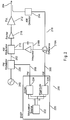
- FIG. 2 is a block diagram illustrating a system 200 for power amplification of an RF signal using polar amplitude feedback.
- the amplification system 200 of Figure 2 includes an amplitude modulator 210, a power amplifier 212, an amplitude detector 214, and a polar amplitude feedback network 216.
- the system 200 also includes a digital signal processor (DSP) 220 and a phase modulator 230.
- DSP 220 provides the original waveform in IQ format via a modulation source 222.
- the DSP also includes arctangent and magnitude functions 224, 226 that isolate the polar phase and magnitude components, respectively, of the original IQ waveform. Based on the output from these functions, the DSP 220 generates a phase component signal 208 and an amplitude component signal 206.
- the phase modulator 230 receives the phase component signal 208 and modulates an RF carrier signal based on the phase component signal 208 to generate a partially-modulated RF signal 202.
- An RF carrier source 240 generates the underlying RF carrier signal.
- the partially-modulated RF signal is phase modulated, but not yet amplitude modulated.
- the amplitude modulator 210 amplitude-modulates the partially-modulated RF signal based on a feedback control signal received from the polar amplitude feedback network 216.
- the resulting completely-modulated RF signal is sent through the exciter 218 to the power amplifier 212 for amplification as an output signal.
- the system 200 includes an amplitude detector 214, which senses the amplitude component of the output signal 104 independent of any phase component.
- the amplitude detector 214 provides a signal indicative of the amplitude component to the polar amplitude feedback network 216.
- the polar amplitude feedback network 216 includes a difference component that generates a polar amplitude feedback control signal based on the difference between the sensed amplitude component of the output signal and the amplitude component 206 of the original waveform.
- the polar amplitude feedback control signal is amplified by a high-gain integrating amplifier 216B and provided to the amplitude modulator 210.
- the amplitude modulator 210 uses the polar amplitude feedback control signal to adjust for any nonlinearities in the amplified output signal 204.
- the amplification system 200 of Figure 2 provides for simple, efficient linear amplification of an RF signal. Because of the high-gain negative feedback present in this configuration, the system will force the detector output to be virtually identical to the desired amplitude modulated waveform. This use of polar amplitude feedback corrects for any distortion introduced by the amplitude modulator 210, the exciter 218, or the power amplifier 212. This enables efficient operation of the power amplifier 212 closer to saturation without the risk of distortion that normally results from operating an amplifier near saturation in an open-loop system. In addition, the components required for the polar amplitude feedback network 216 are relatively simple and inexpensive. However, the phase modulation of the system 200 requires a trade-off for certain applications. Analog phase modulators typically are restricted to +/- 180 degrees of phase shift. Many applications require phase shifts larger than +/- 180 degrees. An alternative configuration is to use a frequency modulator, as shown in Figure 3 .
- FIG 3 is a block diagram illustrating a system 300 for power amplification of an RF signal using polar amplitude feedback.
- the system 300 is similar to the system 200 illustrated in Figure 2 , except that the system 300 includes a frequency modulator 330.
- the DSP 320 of the system 300 includes a differentiator function 328 that isolates the frequency modulated component of the original waveform. Based on the output of this function, the DSP 320 generates a frequency component signal 308, which is passed to the frequency modulator 330.
- the frequency modulator 330 modulates the RF carrier signal based on the frequency component signal 308 to generate a partially-modulated RF signal 302.
- the partially-modulated RF signal 302 is passed to the amplitude modulator 310 for polar feedback-controlled amplitude modulation and amplification, as discussed above with respect to Figure 2 .
- the system 300 shown in Figure 3 includes all of the advantages of the system 200 of Figure 2 , and it is not restricted to phase shifts of less than +/- 180 degrees.
- the frequency processing and modulation required by the system 300 may present challenges for certain applications.
- the differentiation function 328 required to generate the frequency component signal generally uses a finite differential to perform an approximation of the differentiation. This results in a time delay between the amplitude signal component 306 and the frequency component signal 308. This time delay can cause distortion in the output signal 304. Degradations in the signal can be alleviated by performing the differentiation at a very high sample rate to minimize the time delay. However, this process may require excessive processor power and/or speed.
- FIG. 4 is a block diagram illustrating a system 400 for power amplification of an RF signal using polar amplitude feedback.
- the system 400 shown in Figure 4 is similar to the systems 200, 300 of Figures 2 and 3 , except the system 400 includes an IQ modulator 430 in place of a phase/frequency modulator.
- the DSP 420 of the system 400 includes cosine 428A and sine 428B functions, which receive a phase component signal from the arctangent function 424.
- the cosine 428A and sine 428B functions decompose the phase component signal into constant-amplitude in-phase 408A and quadrature 408B component signals.
- These constant-amplitude IQ signals 408A, 408B are passed to the IQ modulator 430, which used them to modulate the RF carrier signal.
- the IQ modulator 430 produces a partially-modulated RF signal 402, which is passed to the amplitude modulator 410.
- the partially-modulated RF signal 402 is phase-modulated because it does not include any of the amplitude information from the original waveform.
- the amplitude information is added via the amplitude modulator 410 and the polar amplitude feedback control network 416.
- the polar amplitude feedback network 416 provides the same advantages of simple, efficient linear amplification described above.
- the system 400 shown in Figure 4 uses three-channel signaling to avoid the limitations of the phase and frequency modulation schemes described above.
- the first of the three channels is polar amplitude.
- the other two channels are the in-phase and quadrature components of the polar phase.
- This three-channel approach permits unlimited phase shifts and avoids the delays caused by the differentiation function required for frequency modulation.
- Figures 5 and 6 illustrate variations on the system 400 shown in Figure 4 .
- the DSP 520 of the system 500 shown in Figure 5 includes a normalization function 528.
- the normalization function 528 divides the IQ signals of the original waveform by the polar amplitude to isolate the in-phase 508A and quadrature 508B components of the polar phase. These signals 508A, 508B are provided to the IQ modulator 530, and the remainder of the system 500 operates just like the system 400 shown in Figure 4 .
- the system 600 of Figure 6 is similar, but lacks the normalization function 528.
- the IQ signals of the original waveform are provided directly to the IQ modulator 630.
- the IQ modulator 630 modulates the RF carrier signal based on both the amplitude and phase of the original waveform and passes the resulting modulated RF signal 602 to the amplitude modulator 610.
- One advantage of this system 600 is that the DSP 620 is simplified compared to the DSPs 420, 520 shown in Figures 4 and 5 . Regardless of the presence or absence of the amplitude component at the input of the amplitude modulator 610, the polar amplitude feedback network 616 still forces the system output to be virtually identical to the desired polar amplitude.
- the remainder of the system 600 operates just like the systems 400, 500 shown in Figures 4 and 5 .
- FIG. 7 is a block diagram illustrating a system 700 for power amplification of an RF signal using polar amplitude feedback and including a single modulator 710.
- the system 700 includes a pair of analog multipliers 750A, 750B that are configured to combine the constant-amplitude IQ phase component signals 708A, 708B with the amplitude feedback control signal from the polar amplitude feedback network 716.
- the combined signals are passed to the single IQ modulator 710 for modulation of the RF carrier signal.
- the remainder of the system 700 including the power amplifier 712, amplitude detector 714, and DSP 720, operate in a manner similar to the systems described above.
- the DSP 828 includes a direct digital synthesis function 828 configured to synthesize the modulated RF signal 802 directly based on the IQ signals of the original waveform.
- the remainder of the system including the amplitude modulator 810, exciter 818, power amplifier 812, amplitude detector 814, and polar amplitude feedback network 816, operate in a manner similar to that described above with respect to Figures 2-6 .
- the polar amplitude feedback forces the output of the amplitude detector to be virtually identical to the desired amplitude output. If the amplitude detector itself is linear, then the detector input and output will be proportional to each other, which means that the system output is virtually identical to the desired amplitude output. However, any nonlinearity introduced by the amplitude detector will cause the system output to be distorted by an equal and opposite amount. As a result, it generally is desirable to use a linear detector.
- IQ demodulators also known as quadrature demodulators
- I-channel of such a demodulator will provide amplitude detection as shown in Figure 9 .
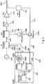
- FIG. 9 is a block diagram illustrating a system 900 for power amplification of an RF signal using polar amplitude feedback and including amplitude detection using an IQ demodulator 914 according to one aspect of the invention.
- the system 900 also includes a fixed phase shifter 960.
- the fixed phase shifter 960 is configured to receive the phase-modulated RF signal 902 from the IQ modulator 930 and to synchronize the phase of the IQ modulator 930 and the local oscillator of the IQ demodulator 914. Because the local oscillator of the IQ demodulator 914 is derived after phase modulation by the IQ modulator 930, the local oscillator will track the phase of the amplified RF output signal 904.
- the remainder of the system 900 of Figure 9 including the DSP 920, IQ modulator 930, amplitude modulator 910, exciter 918, and power amplifier 912, operates in a manner similar to that described above with reference to Figure 4 .
- the I-channel of the IQ demodulator 914 provides pure amplitude detection only if there is no phase distortion introduced by the exciter 918 and the power amplifier 912. If either of these components introduce phase distortion, then ⁇ # 0, and the I-channel of the IQ demodulator 914 will not reflect purely the amplitude component of the amplified RF output signal 904. On the other hand, if the total phase distortion is small, then ⁇ will remain small and cos( ⁇ ) ⁇ 1.
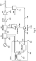
- Figure 10 is a block diagram illustrating a system 1000 for power amplification of an RF signal using full polar feedback and including amplitude and phase detection using an IQ demodulator 1014 according to another aspect of the invention.
- sin( ⁇ ) ⁇ ⁇ so the Q-channel output is proportional to ⁇ for small angles.
- the Q-channel output effectively serves as a phase detector, representing the phase of the amplified RF output signal 1004 relative to the phase of the local oscillator signal. This enables the Q-channel output to serve as a polar phase feedback signal.
- the polar phase feedback signal provided by the Q-channel output is used to control a voltage-controlled phase shifter 1016D. Because of the negative feedback, the phase portion of the full polar feedback network 1016 will force the Q-channel output of the IQ demodulator to be zero.
- the integrating amplifier 1016C causes the voltage-controlled phase shifter 1016D to counter any excess phase introduced by the exciter 1018 or the power amplifier 1012. This provides the added advantage of eliminating any phase distortion that may result from the exciter 1018 and/or the power amplifier 1012.
- ⁇ also is forced to zero, which ensures that the I-channel output of the IQ demodulator accurately tracks the amplitude of the amplified RF output signal 1004.
- the remaining components of the system 1000 operate in a manner similar to that described above with respect to Figures 4 and 9 .
- Variations on the IQ demodulators 914, 1014 and polar feedback networks 916, 1016 shown in Figures 9 and 10 provide various possibilities for polar phase and/or amplitude feedback.
- the phase components 1016C, 1016D of the full polar feedback network 1016 may be used independent of the amplitude components 1016A, 1016B.
- the amplitude components 1016A, 1016B of the full polar feedback network 1016 may be used independent of the phase components 1016C, 1016D (as illustrated in Figure 9 ).
- the amplitude-only feedback network is particularly effective when the exciter 1018 and the power amplifier 1012 introduce little or no phase distortion (i.e., ⁇ is small and cos( ⁇ ) ⁇ 1).
- the complete polar amplitude and phase feedback network 1016 may be employed.
- a linear diode-based amplitude detector may be used in place of the IQ demodulator 1014 and without the phase components 1016C, 1016D of the full polar feedback network 1016.
- a full polar feedback network 1016 provides various advantages compared to traditional Cartesian feedback networks.
- the polar phase and amplitude feedback loops are independent and may be operated together or separately.
- the I and Q feedback loops are interdependent and cannot be independently omitted or disabled.
- the phase ⁇ of the IQ demodulator 1014 shown in Figure 10 is set automatically. Cartesian feedback schemes require an additional control system to set this phase.
- FIG. 11 is a block diagram illustrating a system for power amplification of an RF signal using full polar feedback and including amplitude and phase detection using an IQ modulator according to another aspect of the invention.
- the DSP 1120 shown in Figure 11 provides the IQ signals 1108A, 1108B of the original waveform directly to the IQ modulator 1130.
- the system 1100 may be configured to include two additional components.
- the DSP may be configured to include a 1/A function 1126B, which will be used to isolate the phase component by multiplying the signal by the inverse of its amplitude.
- the output of this function 1126B may then be used to control the second additional component, the amplitude modulator 1162.
- these two components 1126A, 1162 eliminate the amplitude modulation component from the input to the fixed phase shifter 1160.
- the input to the local oscillator of the IQ demodulator 1114 is free of amplitude modulation.
- the remaining components shown in Figure 11 operate in a manner similar to that described above with reference to Figures 9 and 10 .
- Figure 12 is a block diagram illustrating a circuit 1200 for nulling an offset adjustment of a demodulator output buffer.
- the circuit 1200 includes a buffer 1270 for the I-channel output of an IQ demodulator 1214.
- the circuit 1200 may be duplicated for the Q-channel output of the IQ demodulator 1214.
- the buffer 1270 includes an offset-adjust input port that is connected to a two-way switch 1278.
- the switch 1278 selectably connects the offset-adjust input port of the buffer 1270 to either the output of a digital-to-analog converter (DAC) 1276 or to the return end of a feedback loop, including an integrating amplifier 1272 connected to an analog-to-digital converter (ADC) 1274.
- the switch 1278 connects the DAC 1276 output to the offset-adjust input port of the buffer 1270.
- DAC digital-to-analog converter
- ADC analog-to-digital converter
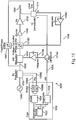
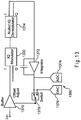
- FIG. 13 is a block diagram illustrating a circuit 1300 for nulling an offset adjustment of a modulator input buffer.
- the circuit 1300 includes a buffer 1370 for the I-channel input of an IQ modulator 1330 paired with a nulled IQ demodulator 1314.
- the circuit 1300 may be duplicated for the Q-channel input of the IQ modulator 1330.
- the buffer 1370 includes an offset-adjust input port that is connected to a two-way switch 1378.
- the switch 1378 selectably connects the offset-adjust input port of the buffer 1370 to either the output of a digital-to-analog converter (DAC) 1376 or to the return end of a feedback loop from the I-channel output of the nulled IQ demodulator, including an integrating amplifier 1372 connected to an analog-to-digital converter (ADC) 1374.
- DAC digital-to-analog converter
- ADC analog-to-digital converter
- the switch connects the DAC output to the offset-adjust input port of the buffer 1370.
- a brief calibration period e.g., ⁇ 1 millisecond
- the switch is set to close the feedback loop, causing feedback to eliminate any leakage in the system.
- the ADC 1374 reads the nulling voltage and sends the value to a controller.
- the controller stores the value and sends it back to the DAC 1376.
- the switch 1378 reverts to its normal position, the desired nulling voltage is applied to the buffer via the DAC 1376.
- the nulling circuits 1200, 1300 shown in Figures 12 and 13 can utilize periodic calibration, depending on how long the modulator/demodulator remains nulled in the normal (i.e., open-loop) mode. For example, if temperature and operation are always consistent, then calibration theoretically may be required only once. Realistically, it usually will be necessary to calibrate the nulling circuits more frequently (e.g., once per hour, once per day, or each time the amplifier/transmitter is turned on).
- the methods and systems of the present invention may be realized in software, hardware, or a combination of software and hardware.
- a typical combination of software and hardware may be a DSP with a program that controls the DSP to perform the functions described herein.
- Any type of computing system or other apparatus adapted for realizing the functions described herein is suitable.
- a program may include any expression, in any language, code or notation, of a set of instructions intended to cause a system having an information processing capability to perform a particular function.
Landscapes
- Engineering & Computer Science (AREA)
- Power Engineering (AREA)
- Physics & Mathematics (AREA)
- Nonlinear Science (AREA)
- Computer Networks & Wireless Communication (AREA)
- Signal Processing (AREA)
- Amplifiers (AREA)
Description
- The invention relates generally to systems for linear amplification of radio-frequency (RF) signals and, more particularly, to systems for linear amplification of RF signals using polar feedback.
- A variety of applications, including many forms of wireless communications, employ radio-frequency (RF) transmissions. For example, an RF carrier wave may be modulated with a baseband signal containing information to be communicated. The modulated RF signal may then be amplified and transmitted. A certain degree of care must be taken in the amplification of the RF signal to ensure that it is not distorted. If the RF transmission is distorted, a receiver may not be able to properly demodulate the RF signal and recover the original baseband signal.
- To avoid distortion, the amplification process must remain relatively linear. One way of accomplishing this is to use a highly backed-off amplifier (i.e., an amplifier operated well below its maximum power capacity). By backing off the amplifier, it may be operated in a relatively linear fashion. However, amplifiers typically operate very inefficiently when backed off far from their maximum capacity.
- Another way to avoid distortion is to use feedback to correct for nonlinearities in the amplified RF signal. The principal of feedback, specifically negative feedback, has been known for decades. High-fidelity audio amplifiers typically use large amounts of negative feedback to reduce audible distortion to very low levels. In principal, direct negative feedback (in which the output is connected back to the input via a passive feedback network) can also be applied to RF amplifiers. However, very high system gain is required to obtain significant linearization. It is relatively easy to obtain high system gain at audio frequencies, but it is not so easy at radio frequencies. As a result, the use of direct negative feedback has been limited in RF power amplifiers, and has provided only marginal results.
- As an alternative to direct negative feedback of an RF signal, the RF signal may be converted to baseband (i.e., a low-frequency signal, similar to audio frequencies) at which high gain may be obtained. The highly amplified baseband signal may then be converted back to RF and applied to the input of an RF amplifier. This process requires demodulating the signal from RF to baseband and then modulating the amplified baseband signal back to RF.
- In a Cartesian feedback system, the demodulation process produces "in-phase" and "quadrature," or "IQ" signals. Cartesian feedback system are sensitive to operating conditions such as temperature and require IQ demodulators and modulators with very tightly controlled phase characteristics. To control the phase characteristics properly, Cartesian feedback requires a complex auxiliary control system that is difficult to implement and adjust. In addition, systems employing Cartesian feedback typically are expensive and complex. As a result, Cartesian feedback is not desirable for certain types of RF applications, such as two-way radio communication.
-
United States Patent Application 2007/0037530 discloses a system in which power amplifier feedback is routed to the power control port of the power amplifier to complete a feedback mechanism. European PatentApplication Publication EP 1 011 192 A2 teaches where feedback from a power amplifier is routed to gain and phase error detectors and the detected gain and phase errors are routed to an adaptive predistorter which provides correction signals to amplitude and phase modulators, thus providing a closed-loop feedback system.United States Patent 6,043,707 teaches a system with feedback from a power amplifier comprising an IQ modulator configured to modulate an RF carrier signal based on a pair of IQ signals representative of at least the phase component of an original waveform, a fixed phase shifter in communication with the IQ modulator; a feedback-controlled amplitude modulator in communication with the power amplifier, an amplitude detector comprising an IQ demodulator in communication with the power amplifier and the fixed phase shifter, wherein a feedback network is configured to generate a feedback control signal. International Patent Application PublicationWO 00/72438 - Accordingly, there is a need for efficient systems for linear amplification of RF signals. In addition, there is a need for relatively simple, inexpensive linear RF amplification systems.
- The solution is provided by a system for power amplification of an RF signal as defined in
claim 1. The system includes a feedback-controlled modulator configured to modulate an RF signal based on a feedback-corrected control signal. The modulator is further configured to generate a modulated RF signal. The system further includes a power amplifier in communication with the modulator. The amplifier is configured to amplify the modulated RF signal and to generate an amplified RF output signal. The system also includes an amplitude detector in communication with the power amplifier. The amplitude detector is configured to detect an amplitude characteristic of the amplified RF output signal and to generate an amplitude feedback signal. The system includes a feedback network in communication with the amplitude detector and the modulator. The feedback network is configured to generate a feedback-corrected control signal based on the difference between the amplitude feedback signal and an amplitude component of the original waveform. - The invention will now be described by way of example with reference to the accompanying drawings. Moreover, in the figures, like referenced numerals designate corresponding parts throughout the different views.
-
Figure 1 is a block diagram illustrating a system for power amplification of an RF signal using polar feedback. -
Figure 2 is a block diagram illustrating a system for power amplification of an RF signal using polar feedback and including a phase modulator. -
Figure 3 is a block diagram illustrating a system for power amplification of an RF signal using polar feedback and including a frequency modulator. -
Figure 4 is a block diagram illustrating a system for power amplification of an RF signal using polar feedback and including an IQ modulator for three-channel signaling. -
Figure 5 is a block diagram illustrating a variation of the system illustrated inFigure 4 . -
Figure 6 is a block diagram illustrating another variation of the system illustrated inFigure 4 . -
Figure 7 is a block diagram illustrating a system for power amplification of an RF signal using polar feedback and including a single modulator. -
Figure 8 is a block diagram illustrating a system for power amplification of an RF signal using polar feedback and including direct digital synthesis. -
Figure 9 is a block diagram illustrating a system for power amplification of an RF signal using polar feedback and including amplitude detection using an IQ demodulator according to one aspect of the invention. -
Figure 10 is a block diagram illustrating a system for power amplification of an RF signal using polar feedback and including amplitude and phase detection using an IQ demodulator according to another aspect of the invention. -
Figure 11 is a block diagram illustrating a system for power amplification of an RF signal using polar feedback and including amplitude and phase detection using an IQ modulator according to another aspect of the invention. -
Figure 12 is a block diagram illustrating a circuit for nulling an offset adjustment of a demodulator output buffer. -
Figure 13 is a block diagram illustrating a circuit for nulling an offset adjustment of a modulator input buffer. - Embodiments of the invention include systems for power amplification of an RF signal, including amplifiers, transmitters, etc. The embodiments described in this application may be implemented in a wide range of applications, such as, for example, two-way radios, simulcast communication systems, and mobile telephones.
-
Figure 1 is a block diagram illustrating asystem 100 for linear amplification using polar amplitude feedback. Polar amplitude feedback is provided based on the magnitude channel of a polar feedback network. Thesystem 100 modulates and amplifies anRF signal 102 to generate anoutput signal 104. The modulation is provided by anamplitude modulator 110, and the amplification is provided by apower amplifier 112. Theamplitude modulator 110 and thepower amplifier 112 may take any suitable form, depending on the particular application. For example, the modulation and amplification functions may be combined into a single device or distributed among many devices. In addition, the power amplifier 112 (or power amplifiers) need not be linear in operation. Thesystem 100 includes a polaramplitude feedback network 116 to correct for any distortion or nonlinearities introduced by thepower amplifier 112. - An
amplitude detector 114 senses the amplitude component of theoutput signal 104 independent of any phase component. For example, theamplitude detector 114 may be a signal envelope detector. Theamplitude detector 114 provides a signal indicative of the amplitude component to the polaramplitude feedback network 116. The polaramplitude feedback network 116 includes afeedback control 116A. In addition to the amplitude component of theoutput signal 104, thefeedback control 116A also receives asignal 106 representing the amplitude component of the original input waveform. Based on these two signals, thefeedback control 116A generates a polar amplitude feedback control signal and provides this signal to theamplitude modulator 110. Theamplitude modulator 110 uses the polar amplitude feedback control signal to adjust for any nonlinearities in the amplifiedoutput signal 104. - The
incoming RF signal 102 may already be partially modulated before reaching theamplitude modulator 110. For example, theincoming RF signal 102 may have been modulated previously using phase information from the original waveform. Alternatively, theincoming RF signal 102 may have been modulated previously using both phase and amplitude information from the original waveform. Examples of these alternatives are described in more detail below. -
Figure 2 is a block diagram illustrating asystem 200 for power amplification of an RF signal using polar amplitude feedback. Like thesystem 100 illustrated inFigure 1 , theamplification system 200 ofFigure 2 includes anamplitude modulator 210, apower amplifier 212, anamplitude detector 214, and a polaramplitude feedback network 216. Thesystem 200 also includes a digital signal processor (DSP) 220 and aphase modulator 230. TheDSP 220 provides the original waveform in IQ format via amodulation source 222. The DSP also includes arctangent and magnitude functions 224, 226 that isolate the polar phase and magnitude components, respectively, of the original IQ waveform. Based on the output from these functions, theDSP 220 generates aphase component signal 208 and anamplitude component signal 206. - The
phase modulator 230 receives thephase component signal 208 and modulates an RF carrier signal based on thephase component signal 208 to generate a partially-modulatedRF signal 202. AnRF carrier source 240 generates the underlying RF carrier signal. In the system illustrated inFigure 2 , the partially-modulated RF signal is phase modulated, but not yet amplitude modulated. Theamplitude modulator 210 amplitude-modulates the partially-modulated RF signal based on a feedback control signal received from the polaramplitude feedback network 216. The resulting completely-modulated RF signal is sent through theexciter 218 to thepower amplifier 212 for amplification as an output signal. - As in the
system 100 shown inFigure 1 , thesystem 200 includes anamplitude detector 214, which senses the amplitude component of theoutput signal 104 independent of any phase component. Theamplitude detector 214 provides a signal indicative of the amplitude component to the polaramplitude feedback network 216. The polaramplitude feedback network 216 includes a difference component that generates a polar amplitude feedback control signal based on the difference between the sensed amplitude component of the output signal and theamplitude component 206 of the original waveform. The polar amplitude feedback control signal is amplified by a high-gain integrating amplifier 216B and provided to theamplitude modulator 210. Theamplitude modulator 210 uses the polar amplitude feedback control signal to adjust for any nonlinearities in the amplifiedoutput signal 204. - The
amplification system 200 ofFigure 2 provides for simple, efficient linear amplification of an RF signal. Because of the high-gain negative feedback present in this configuration, the system will force the detector output to be virtually identical to the desired amplitude modulated waveform. This use of polar amplitude feedback corrects for any distortion introduced by theamplitude modulator 210, theexciter 218, or thepower amplifier 212. This enables efficient operation of thepower amplifier 212 closer to saturation without the risk of distortion that normally results from operating an amplifier near saturation in an open-loop system. In addition, the components required for the polaramplitude feedback network 216 are relatively simple and inexpensive. However, the phase modulation of thesystem 200 requires a trade-off for certain applications. Analog phase modulators typically are restricted to +/- 180 degrees of phase shift. Many applications require phase shifts larger than +/- 180 degrees. An alternative configuration is to use a frequency modulator, as shown inFigure 3 . -
Figure 3 is a block diagram illustrating asystem 300 for power amplification of an RF signal using polar amplitude feedback. Thesystem 300 is similar to thesystem 200 illustrated inFigure 2 , except that thesystem 300 includes afrequency modulator 330. In addition, theDSP 320 of thesystem 300 includes adifferentiator function 328 that isolates the frequency modulated component of the original waveform. Based on the output of this function, theDSP 320 generates afrequency component signal 308, which is passed to thefrequency modulator 330. Thefrequency modulator 330 modulates the RF carrier signal based on thefrequency component signal 308 to generate a partially-modulatedRF signal 302. The partially-modulatedRF signal 302 is passed to theamplitude modulator 310 for polar feedback-controlled amplitude modulation and amplification, as discussed above with respect toFigure 2 . - The
system 300 shown inFigure 3 includes all of the advantages of thesystem 200 ofFigure 2 , and it is not restricted to phase shifts of less than +/- 180 degrees. However, the frequency processing and modulation required by thesystem 300 may present challenges for certain applications. Thedifferentiation function 328 required to generate the frequency component signal generally uses a finite differential to perform an approximation of the differentiation. This results in a time delay between theamplitude signal component 306 and thefrequency component signal 308. This time delay can cause distortion in theoutput signal 304. Degradations in the signal can be alleviated by performing the differentiation at a very high sample rate to minimize the time delay. However, this process may require excessive processor power and/or speed. - As an alternative to the phase and frequency modulators discussed above, an IQ modulator may be used to perform the initial RF modulation. For example,
Figure 4 is a block diagram illustrating asystem 400 for power amplification of an RF signal using polar amplitude feedback. Thesystem 400 shown inFigure 4 is similar to thesystems Figures 2 and3 , except thesystem 400 includes anIQ modulator 430 in place of a phase/frequency modulator. In addition, theDSP 420 of thesystem 400 includescosine 428A andsine 428B functions, which receive a phase component signal from thearctangent function 424. Thecosine 428A andsine 428B functions decompose the phase component signal into constant-amplitude in-phase 408A andquadrature 408B component signals. These constant-amplitude IQ signals 408A, 408B are passed to theIQ modulator 430, which used them to modulate the RF carrier signal. TheIQ modulator 430 produces a partially-modulatedRF signal 402, which is passed to theamplitude modulator 410. In effect, the partially-modulatedRF signal 402 is phase-modulated because it does not include any of the amplitude information from the original waveform. As with the system described above, the amplitude information is added via theamplitude modulator 410 and the polar amplitudefeedback control network 416. The polaramplitude feedback network 416 provides the same advantages of simple, efficient linear amplification described above. - The
system 400 shown inFigure 4 uses three-channel signaling to avoid the limitations of the phase and frequency modulation schemes described above. The first of the three channels is polar amplitude. The other two channels are the in-phase and quadrature components of the polar phase. This three-channel approach permits unlimited phase shifts and avoids the delays caused by the differentiation function required for frequency modulation. -
Figures 5 and6 illustrate variations on thesystem 400 shown inFigure 4 . In place of arctangent, cosine, and sine functions, theDSP 520 of thesystem 500 shown inFigure 5 includes anormalization function 528. Thenormalization function 528 divides the IQ signals of the original waveform by the polar amplitude to isolate the in-phase 508A andquadrature 508B components of the polar phase. Thesesignals 508A, 508B are provided to theIQ modulator 530, and the remainder of thesystem 500 operates just like thesystem 400 shown inFigure 4 . - The
system 600 ofFigure 6 is similar, but lacks thenormalization function 528. In thissystem 600, the IQ signals of the original waveform are provided directly to theIQ modulator 630. As a result, theIQ modulator 630 modulates the RF carrier signal based on both the amplitude and phase of the original waveform and passes the resulting modulatedRF signal 602 to theamplitude modulator 610. One advantage of thissystem 600 is that theDSP 620 is simplified compared to theDSPs Figures 4 and5 . Regardless of the presence or absence of the amplitude component at the input of theamplitude modulator 610, the polaramplitude feedback network 616 still forces the system output to be virtually identical to the desired polar amplitude. The remainder of thesystem 600 operates just like thesystems Figures 4 and5 . - Another alternative to the systems described above is to combine the functions of the IQ and amplitude modulators. For example,
Figure 7 is a block diagram illustrating asystem 700 for power amplification of an RF signal using polar amplitude feedback and including asingle modulator 710. Thesystem 700 includes a pair ofanalog multipliers amplitude feedback network 716. The combined signals are passed to thesingle IQ modulator 710 for modulation of the RF carrier signal. The remainder of thesystem 700, including thepower amplifier 712,amplitude detector 714, andDSP 720, operate in a manner similar to the systems described above. - Yet another alternative amplification system, shown in
Figure 8 , employs direct digital synthesis in place of the initial phase modulation. TheDSP 828 includes a directdigital synthesis function 828 configured to synthesize the modulated RF signal 802 directly based on the IQ signals of the original waveform. The remainder of the system, including theamplitude modulator 810,exciter 818,power amplifier 812,amplitude detector 814, and polaramplitude feedback network 816, operate in a manner similar to that described above with respect toFigures 2-6 . - In all of the systems described above, the polar amplitude feedback forces the output of the amplitude detector to be virtually identical to the desired amplitude output. If the amplitude detector itself is linear, then the detector input and output will be proportional to each other, which means that the system output is virtually identical to the desired amplitude output. However, any nonlinearity introduced by the amplitude detector will cause the system output to be distorted by an equal and opposite amount. As a result, it generally is desirable to use a linear detector.
- Very linear diode-based amplitude detectors are available and are suitable for use with the systems described here. In general, however, synchronous amplitude detectors are more linear than typical diode detectors. IQ demodulators (also known as quadrature demodulators) typically are composed of two synchronous detectors, one with in-phase oscillator injection, and the other with quadrature oscillator injection. The I-channel of such a demodulator will provide amplitude detection as shown in
Figure 9 . -
Figure 9 is a block diagram illustrating asystem 900 for power amplification of an RF signal using polar amplitude feedback and including amplitude detection using anIQ demodulator 914 according to one aspect of the invention. In addition to theIQ demodulator 914, thesystem 900 also includes afixed phase shifter 960. Thefixed phase shifter 960 is configured to receive the phase-modulated RF signal 902 from theIQ modulator 930 and to synchronize the phase of theIQ modulator 930 and the local oscillator of theIQ demodulator 914. Because the local oscillator of theIQ demodulator 914 is derived after phase modulation by theIQ modulator 930, the local oscillator will track the phase of the amplifiedRF output signal 904. - The I-channel output of the
IQ demodulator 914 is proportional to A*cos(θ), where A is the amplitude of the demodulator's input, and θ is the phase of the demodulator's input referenced to the phase of its local oscillator. Because of the phase tracking described above, θ = 0, so cos(θ) = 1. As a result, the I-channel output is proportional to A, the amplitude of the input. In this way, the I-channel of thedemodulator 914 provides an effective amplitude feedback signal for the polaramplitude feedback network 916. The remainder of thesystem 900 ofFigure 9 , including theDSP 920,IQ modulator 930,amplitude modulator 910,exciter 918, andpower amplifier 912, operates in a manner similar to that described above with reference toFigure 4 . - The I-channel of the
IQ demodulator 914 provides pure amplitude detection only if there is no phase distortion introduced by theexciter 918 and thepower amplifier 912. If either of these components introduce phase distortion, then θ # 0, and the I-channel of theIQ demodulator 914 will not reflect purely the amplitude component of the amplifiedRF output signal 904. On the other hand, if the total phase distortion is small, then θ will remain small and cos(θ) ≈ 1. - To ensure that θ = 0, the
system 900 ofFigure 9 may be modified to include full polar feedback, including polar phase feedback. For example,Figure 10 is a block diagram illustrating asystem 1000 for power amplification of an RF signal using full polar feedback and including amplitude and phase detection using anIQ demodulator 1014 according to another aspect of the invention. The Q-channel output of theIQ demodulator 1014 is proportional to A*sin(θ). This output equals zero as long as θ = 0. For small angles, however, sin(θ) ≈ θ, so the Q-channel output is proportional to θ for small angles. As a result, the Q-channel output effectively serves as a phase detector, representing the phase of the amplifiedRF output signal 1004 relative to the phase of the local oscillator signal. This enables the Q-channel output to serve as a polar phase feedback signal. - After amplification by an integrating
amplifier 1016C, the polar phase feedback signal provided by the Q-channel output is used to control a voltage-controlledphase shifter 1016D. Because of the negative feedback, the phase portion of the fullpolar feedback network 1016 will force the Q-channel output of the IQ demodulator to be zero. In this scheme, the integratingamplifier 1016C causes the voltage-controlledphase shifter 1016D to counter any excess phase introduced by theexciter 1018 or thepower amplifier 1012. This provides the added advantage of eliminating any phase distortion that may result from theexciter 1018 and/or thepower amplifier 1012. In the process, θ also is forced to zero, which ensures that the I-channel output of the IQ demodulator accurately tracks the amplitude of the amplifiedRF output signal 1004. The remaining components of thesystem 1000 operate in a manner similar to that described above with respect toFigures 4 and9 . - Variations on the
IQ demodulators polar feedback networks Figures 9 and10 provide various possibilities for polar phase and/or amplitude feedback. For example, thephase components polar feedback network 1016 may be used independent of theamplitude components amplitude components polar feedback network 1016 may be used independent of thephase components Figure 9 ). The amplitude-only feedback network is particularly effective when theexciter 1018 and thepower amplifier 1012 introduce little or no phase distortion (i.e., θ is small and cos(θ) ≈ 1). If phase distortion from either or both of these components is significant, the complete polar amplitude andphase feedback network 1016 may be employed. Alternatively, a linear diode-based amplitude detector may be used in place of theIQ demodulator 1014 and without thephase components polar feedback network 1016. - The use of a full
polar feedback network 1016 provides various advantages compared to traditional Cartesian feedback networks. For example, the polar phase and amplitude feedback loops are independent and may be operated together or separately. In a traditional Cartesian feedback network, the I and Q feedback loops are interdependent and cannot be independently omitted or disabled. In addition, the phase θ of theIQ demodulator 1014 shown inFigure 10 is set automatically. Cartesian feedback schemes require an additional control system to set this phase. - A full polar feedback network also may be applied to the
amplification system 600 shown inFigure 6 . For example,Figure 11 is a block diagram illustrating a system for power amplification of an RF signal using full polar feedback and including amplitude and phase detection using an IQ modulator according to another aspect of the invention. As with thesystem 600 ofFigure 6 , theDSP 1120 shown inFigure 11 provides the IQ signals 1108A, 1108B of the original waveform directly to theIQ modulator 1130. In some applications, it may be undesirable for the local oscillator of theIQ demodulator 1114 to receive an input that includes an amplitude modulation component. To avoid this, thesystem 1100 may be configured to include two additional components. First, the DSP may be configured to include a 1/Afunction 1126B, which will be used to isolate the phase component by multiplying the signal by the inverse of its amplitude. The output of thisfunction 1126B may then be used to control the second additional component, theamplitude modulator 1162. Together, these twocomponents fixed phase shifter 1160. As a result, the input to the local oscillator of theIQ demodulator 1114 is free of amplitude modulation. The remaining components shown inFigure 11 operate in a manner similar to that described above with reference toFigures 9 and10 . - Some types of amplitude modulators experience excessive levels of carrier leakage. In addition, certain IQ demodulators experience excessive DC offset levels. To address these issues, a nulling circuit may be used in applications and situations in which leakage and/or offset presents a problem. For example,
Figure 12 is a block diagram illustrating acircuit 1200 for nulling an offset adjustment of a demodulator output buffer. Thecircuit 1200 includes abuffer 1270 for the I-channel output of anIQ demodulator 1214. Thecircuit 1200 may be duplicated for the Q-channel output of theIQ demodulator 1214. Thebuffer 1270 includes an offset-adjust input port that is connected to a two-way switch 1278. Theswitch 1278 selectably connects the offset-adjust input port of thebuffer 1270 to either the output of a digital-to-analog converter (DAC) 1276 or to the return end of a feedback loop, including an integratingamplifier 1272 connected to an analog-to-digital converter (ADC) 1274. During normal operation, theswitch 1278 connects theDAC 1276 output to the offset-adjust input port of thebuffer 1270. During a brief calibration period (e.g., << 1 millisecond), the switch is set to close the feedback loop, causing feedback to cancel any offset in the system. During calibration, theADC 1274 reads the nulling voltage and sends the value to a controller. The controller stores the value and sends it back to theDAC 1276. When the calibration period is over, and the switch reverts to its normal position, the desired nulling voltage is applied to the buffer via theDAC 1276. - Once the IQ demodulator is nulled, a similar scheme can be applied around the modulator-demodulator combination to null any leakage of the modulator. In this case, feedback may be applied to an input buffer that precedes the modulator. For example,
Figure 13 is a block diagram illustrating acircuit 1300 for nulling an offset adjustment of a modulator input buffer. Thecircuit 1300 includes abuffer 1370 for the I-channel input of anIQ modulator 1330 paired with a nulledIQ demodulator 1314. Thecircuit 1300 may be duplicated for the Q-channel input of theIQ modulator 1330. Thebuffer 1370 includes an offset-adjust input port that is connected to a two-way switch 1378. Operation of theswitch 1378 is similar to that of theswitch 1278 described above with reference toFigure 12 . Theswitch 1378 selectably connects the offset-adjust input port of thebuffer 1370 to either the output of a digital-to-analog converter (DAC) 1376 or to the return end of a feedback loop from the I-channel output of the nulled IQ demodulator, including an integratingamplifier 1372 connected to an analog-to-digital converter (ADC) 1374. During normal operation, the switch connects the DAC output to the offset-adjust input port of thebuffer 1370. During a brief calibration period (e.g., << 1 millisecond), the switch is set to close the feedback loop, causing feedback to eliminate any leakage in the system. During calibration, theADC 1374 reads the nulling voltage and sends the value to a controller. The controller stores the value and sends it back to theDAC 1376. When the calibration period is over, and theswitch 1378 reverts to its normal position, the desired nulling voltage is applied to the buffer via theDAC 1376. - The
nulling circuits Figures 12 and13 can utilize periodic calibration, depending on how long the modulator/demodulator remains nulled in the normal (i.e., open-loop) mode. For example, if temperature and operation are always consistent, then calibration theoretically may be required only once. Realistically, it usually will be necessary to calibrate the nulling circuits more frequently (e.g., once per hour, once per day, or each time the amplifier/transmitter is turned on). - The methods and systems of the present invention may be realized in software, hardware, or a combination of software and hardware. For example, a typical combination of software and hardware may be a DSP with a program that controls the DSP to perform the functions described herein. Any type of computing system or other apparatus adapted for realizing the functions described herein is suitable. In the present context, a program may include any expression, in any language, code or notation, of a set of instructions intended to cause a system having an information processing capability to perform a particular function.
- It is intended that the foregoing detailed description be regarded as illustrative rather than limiting, and that it be understood that the following claims, including all equivalents, are intended to define the scope of this invention. One of ordinary skill in the art will recognize that variations on the systems and methods described herein may be made within the scope of the, as will be apparent to those reasonably skilled in the art.
Claims (7)
- A system (900, 1000, 1100) for power amplification of a radio-frequency (RF) signal, comprising:an IQ modulator (930) configured to modulate an RF carrier signal based on a pair of IQ signals (908A,B) representative of at least the phase component of an original waveform to generate a phase-modulated RF signal (902, 1002, 1102);a fixed phase shifter (960, 1060) in communication with the IQ modulator and configured to generate a phase shift signal based on a phase characteristic of the phase-modulated RF signal (902, 1002, 1102);a feedback-controlled amplitude modulator (910, 1010, 1110) in communication with the IQ modulator and configured to modulate the phase-modulated RF signal (902, 1002, 1102) based on a feedback-corrected control signal to generate a modulated RF signal;a power amplifier (912, 1012, 1112) in communication with the amplitude modulator, wherein the power amplifier is configured to amplify the modulated RF signal and to generate an amplified RF output signal (904, 1004, 1104);an amplitude detector comprising an IQ demodulator (914, 1014) in communication with the power amplifier and the fixed phase shifter, wherein the fixed phase shifter is configured to receive the phase-modulated RF signal (902, 1002, 1102) from the IQ modulator (930) and to synchronise a phase of the IQ modulator (930) and a local oscillator of the IQ demodulator (914, 1014), and wherein the amplitude detector is configured to receive the phase shift signal, to detect an amplitude characteristic of the amplified RF output signal and to generate an amplitude feedback signal; anda feedback network (916, 1016, 1116) in communication with the amplitude detector and the amplitude modulator, wherein the feedback network is configured to generate the feedback-corrected control signal based on a difference between the amplitude feedback signal and an amplitude component (1006, 1106) of the original waveform.
- A system as in claim 1, wherein
the feedback-corrected control signal is a feedback-corrected amplitude control signal. - The system of claim 1, further comprising a digital signal processor (420) in communication with the IQ modulator, wherein the digital signal processor is configured to normalize the pair of IQ signals to represent only the phase component of the original waveform.
- The system of claim 1, further comprising:a polar signal converter (424, 426) configured to receive the original waveform in a rectangular format, to convert the original waveform into the phase component and the amplitude component, and to provide the amplitude component to the feedback network; anda rectangular signal converter (428A,B) in communication with the polar signal converter and the first modulator, wherein the rectangular signal converter is configured to convert the phase component into the pair of IQ signals.
- The system of claim 4, wherein the polar signal converter and the rectangular signal converter are implemented in a digital signal processor (420).
- A system as in claim 1, wherein:the feedback-corrected control signal comprises a pair of feedback-corrected IQ signals;the feedback network includes a pair of analog multipliers (1016B, 1016C) configured to generate the feedback-corrected IQ signals based on(i) a pair of IQ signals representative of at least the phase component of the original waveform; and(ii) the difference between the amplitude feedback signal and the amplitude component of the original waveform.
- The system of claim 1,
wherein the IQ demodulator includes a local oscillator configured to receive the phase shift signal and to oscillate in phase with the phase-modulated RF signal (902, 1002, 1102); and
wherein the amplitude feedback signal further comprises an in-phase component signal generated by the IQ demodulator based on the amplified RF output signal.
Applications Claiming Priority (2)
| Application Number | Priority Date | Filing Date | Title |
|---|---|---|---|
| US11/801,444 US7890067B2 (en) | 2007-05-10 | 2007-05-10 | Linear RF amplifier with polar feedback |
| PCT/US2008/005886 WO2008140730A1 (en) | 2007-05-10 | 2008-05-08 | Linear rf amplifier with polar feedback |
Publications (3)
| Publication Number | Publication Date |
|---|---|
| EP2151047A1 EP2151047A1 (en) | 2010-02-10 |
| EP2151047B1 true EP2151047B1 (en) | 2017-09-06 |
| EP2151047B8 EP2151047B8 (en) | 2017-10-11 |
Family
ID=39681031
Family Applications (1)
| Application Number | Title | Priority Date | Filing Date |
|---|---|---|---|
| EP08754245.2A Active EP2151047B8 (en) | 2007-05-10 | 2008-05-08 | Linear rf amplifier with polar feedback |
Country Status (6)
| Country | Link |
|---|---|
| US (1) | US7890067B2 (en) |
| EP (1) | EP2151047B8 (en) |
| JP (2) | JP2010527202A (en) |
| KR (1) | KR101089028B1 (en) |
| CN (1) | CN101803182B (en) |
| WO (1) | WO2008140730A1 (en) |
Families Citing this family (7)
| Publication number | Priority date | Publication date | Assignee | Title |
|---|---|---|---|---|
| GB2412512B (en) * | 2002-05-31 | 2005-11-16 | Renesas Tech Corp | A communication semiconductor integrated circuit, a wireless communication apparatus, and a loop gain calibration method |
| KR101481507B1 (en) * | 2007-03-12 | 2015-01-13 | 엘지전자 주식회사 | Method For Transmitting and Receiving Additional Control Signals |
| JP2009232425A (en) * | 2008-03-25 | 2009-10-08 | Toshiba Corp | Transmitter |
| US9264005B1 (en) * | 2012-07-06 | 2016-02-16 | Marvell International Ltd. | Techniques for efficient radio frequency power amplifier |
| CN103036578B (en) * | 2012-12-25 | 2014-11-12 | 上海贝岭股份有限公司 | Transmitting terminal circuit for high speed digital communication |
| CN105445682B (en) * | 2014-07-25 | 2018-08-21 | 通用电气公司 | MR imaging apparatus, radio frequency amplification system and method |
| CN105187346B (en) * | 2015-09-25 | 2019-03-05 | 海能达通信股份有限公司 | The method and transmitter that transmitter phase adaptively adjusts |
Family Cites Families (13)
| Publication number | Priority date | Publication date | Assignee | Title |
|---|---|---|---|---|
| GB2135546B (en) * | 1983-02-23 | 1986-03-19 | Philips Electronic Associated | Polar loop transmitter |
| GB2150378B (en) * | 1983-11-21 | 1987-06-03 | Philips Electronic Associated | Polar loop transmitter |
| US6295442B1 (en) * | 1998-12-07 | 2001-09-25 | Ericsson Inc. | Amplitude modulation to phase modulation cancellation method in an RF amplifier |
| US6275685B1 (en) * | 1998-12-10 | 2001-08-14 | Nortel Networks Limited | Linear amplifier arrangement |
| US6043707A (en) * | 1999-01-07 | 2000-03-28 | Motorola, Inc. | Method and apparatus for operating a radio-frequency power amplifier as a variable-class linear amplifier |
| EP1181768B1 (en) | 1999-05-25 | 2004-11-24 | Nokia Corporation | Linearisation and modulation device |
| GB2370169A (en) * | 2000-12-15 | 2002-06-19 | Nokia Mobile Phones Ltd | Radio transmitter circuits |
| GB2412513B (en) * | 2002-05-31 | 2006-03-08 | Renesas Tech Corp | Apparatus for radio telecommunication system and method of building up output power |
| US7072626B2 (en) * | 2003-04-30 | 2006-07-04 | Telefonaktiebolaget Lm Ericsson (Publ) | Polar modulation transmitter |
| US7539462B2 (en) * | 2005-08-09 | 2009-05-26 | Freescale Semiconductor, Inc. | Configurable multi-mode modulation system and transmitter |
| US7860466B2 (en) * | 2006-06-04 | 2010-12-28 | Samsung Electro-Mechanics Company, Ltd. | Systems, methods, and apparatuses for linear polar transmitters |
| US7558542B2 (en) * | 2006-06-09 | 2009-07-07 | Mediatek Inc. | System and method for providing a transmitter for polar modulation and power amplifier linearization |
| US7570928B2 (en) * | 2006-08-04 | 2009-08-04 | Axiom Microdevices, Inc. | System and method for low delay corrective feedback power amplifier control |
-
2007
- 2007-05-10 US US11/801,444 patent/US7890067B2/en active Active
-
2008
- 2008-05-08 EP EP08754245.2A patent/EP2151047B8/en active Active
- 2008-05-08 WO PCT/US2008/005886 patent/WO2008140730A1/en not_active Ceased
- 2008-05-08 KR KR1020097025299A patent/KR101089028B1/en active Active
- 2008-05-08 JP JP2010507455A patent/JP2010527202A/en active Pending
- 2008-05-08 CN CN2008800215928A patent/CN101803182B/en not_active Expired - Fee Related
-
2011
- 2011-04-25 JP JP2011096736A patent/JP5248651B2/en active Active
Non-Patent Citations (1)
| Title |
|---|
| None * |
Also Published As
| Publication number | Publication date |
|---|---|
| US20080280573A1 (en) | 2008-11-13 |
| US7890067B2 (en) | 2011-02-15 |
| KR101089028B1 (en) | 2011-12-01 |
| EP2151047A1 (en) | 2010-02-10 |
| CN101803182A (en) | 2010-08-11 |
| WO2008140730A1 (en) | 2008-11-20 |
| JP2010527202A (en) | 2010-08-05 |
| CN101803182B (en) | 2013-05-22 |
| EP2151047B8 (en) | 2017-10-11 |
| KR20100002302A (en) | 2010-01-06 |
| JP5248651B2 (en) | 2013-07-31 |
| JP2011142696A (en) | 2011-07-21 |
Similar Documents
| Publication | Publication Date | Title |
|---|---|---|
| JP2967699B2 (en) | Transmission device | |
| FI105506B (en) | Linearization procedure for amplifiers and amplifier arrangements | |
| JP4327848B2 (en) | Adjustment of amplitude and phase characteristics of wireless communication signals generated by transmitters | |
| US7915954B2 (en) | Amplifier predistortion and autocalibration method and apparatus | |
| US5894496A (en) | Method and apparatus for detecting and compensating for undesired phase shift in a radio transceiver | |
| US7346122B1 (en) | Direct modulation of a power amplifier with adaptive digital predistortion | |
| US6647073B2 (en) | Linearisation and modulation device | |
| US7890067B2 (en) | Linear RF amplifier with polar feedback | |
| JP3910167B2 (en) | Amplifier circuit | |
| US20090096521A1 (en) | Power amplifier predistortion methods and apparatus using envelope and phase detector | |
| WO2007089994A2 (en) | Supply voltage control for a power amplifier | |
| US20040132470A1 (en) | Amplitude- and frequency- or phase-modulated radio frequency signal generator and the transmitter incorporating same | |
| JPWO2006051776A1 (en) | Amplifier circuit, wireless communication circuit, wireless base station device, and wireless terminal device | |
| US20150061762A1 (en) | Dual power amplifier linearizer | |
| JP3710253B2 (en) | Distortion compensation system | |
| CN101442511A (en) | Method and apparatus for improving radio frequency index of zero intermediate frequency transmitter | |
| CA2088750C (en) | Linearized output control of a nonlinear amplifier | |
| US4870374A (en) | Modulator producing phase modulation by combining amplitude modulated signals | |
| JP2003524339A (en) | Communication system with predistortion processing | |
| US6680648B2 (en) | High power amplifier predistorter system | |
| JPH08251246A (en) | Transmitter | |
| JP4686412B2 (en) | Wireless communication device | |
| KR20110068701A (en) | Method and apparatus for linearizing power amplifier in polar transmitter | |
| JP3407243B2 (en) | Wireless device and distortion compensation method | |
| JPH04291829A (en) | Distortion compensation circuit |
Legal Events
| Date | Code | Title | Description |
|---|---|---|---|
| PUAI | Public reference made under article 153(3) epc to a published international application that has entered the european phase |
Free format text: ORIGINAL CODE: 0009012 |
|
| 17P | Request for examination filed |
Effective date: 20091210 |
|
| AK | Designated contracting states |
Kind code of ref document: A1 Designated state(s): AT BE BG CH CY CZ DE DK EE ES FI FR GB GR HR HU IE IS IT LI LT LU LV MC MT NL NO PL PT RO SE SI SK TR |
|
| AX | Request for extension of the european patent |
Extension state: AL BA MK RS |
|
| 17Q | First examination report despatched |
Effective date: 20100222 |
|
| DAX | Request for extension of the european patent (deleted) | ||
| GRAP | Despatch of communication of intention to grant a patent |
Free format text: ORIGINAL CODE: EPIDOSNIGR1 |
|
| RIC1 | Information provided on ipc code assigned before grant |
Ipc: H04L 27/36 20060101ALI20170321BHEP Ipc: H04B 1/04 20060101ALI20170321BHEP Ipc: H03F 1/02 20060101ALI20170321BHEP Ipc: H03F 3/189 20060101AFI20170321BHEP Ipc: H03C 5/00 20060101ALI20170321BHEP Ipc: H03C 3/40 20060101ALI20170321BHEP Ipc: H03F 3/24 20060101ALI20170321BHEP Ipc: H03F 1/32 20060101ALI20170321BHEP |
|
| INTG | Intention to grant announced |
Effective date: 20170404 |
|
| GRAS | Grant fee paid |
Free format text: ORIGINAL CODE: EPIDOSNIGR3 |
|
| GRAA | (expected) grant |
Free format text: ORIGINAL CODE: 0009210 |
|
| AK | Designated contracting states |
Kind code of ref document: B1 Designated state(s): AT BE BG CH CY CZ DE DK EE ES FI FR GB GR HR HU IE IS IT LI LT LU LV MC MT NL NO PL PT RO SE SI SK TR |
|
| REG | Reference to a national code |
Ref country code: GB Ref legal event code: FG4D |
|
| REG | Reference to a national code |
Ref country code: CH Ref legal event code: EP Ref country code: AT Ref legal event code: REF Ref document number: 926912 Country of ref document: AT Kind code of ref document: T Effective date: 20170915 |
|
| RAP2 | Party data changed (patent owner data changed or rights of a patent transferred) |
Owner name: EAGLE TECHNOLOGY, LLC |
|
| REG | Reference to a national code |
Ref country code: DE Ref legal event code: R082 Ref document number: 602008052015 Country of ref document: DE Representative=s name: WUESTHOFF & WUESTHOFF, PATENTANWAELTE PARTG MB, DE Ref country code: DE Ref legal event code: R081 Ref document number: 602008052015 Country of ref document: DE Owner name: EAGLE TECHNOLOGY, LLC (N.D.GES. DES STAATES DE, US Free format text: FORMER OWNER: PINE VALLEY INVESTMENTS, INC., LAS VEGAS, NEV., US Ref country code: IE Ref legal event code: FG4D |
|
| REG | Reference to a national code |
Ref country code: DE Ref legal event code: R096 Ref document number: 602008052015 Country of ref document: DE |
|
| REG | Reference to a national code |
Ref country code: GB Ref legal event code: 732E Free format text: REGISTERED BETWEEN 20171109 AND 20171115 |
|
| REG | Reference to a national code |
Ref country code: NL Ref legal event code: MP Effective date: 20170906 |
|
| REG | Reference to a national code |
Ref country code: LT Ref legal event code: MG4D |
|
| PG25 | Lapsed in a contracting state [announced via postgrant information from national office to epo] |
Ref country code: LT Free format text: LAPSE BECAUSE OF FAILURE TO SUBMIT A TRANSLATION OF THE DESCRIPTION OR TO PAY THE FEE WITHIN THE PRESCRIBED TIME-LIMIT Effective date: 20170906 Ref country code: HR Free format text: LAPSE BECAUSE OF FAILURE TO SUBMIT A TRANSLATION OF THE DESCRIPTION OR TO PAY THE FEE WITHIN THE PRESCRIBED TIME-LIMIT Effective date: 20170906 Ref country code: SE Free format text: LAPSE BECAUSE OF FAILURE TO SUBMIT A TRANSLATION OF THE DESCRIPTION OR TO PAY THE FEE WITHIN THE PRESCRIBED TIME-LIMIT Effective date: 20170906 Ref country code: NO Free format text: LAPSE BECAUSE OF FAILURE TO SUBMIT A TRANSLATION OF THE DESCRIPTION OR TO PAY THE FEE WITHIN THE PRESCRIBED TIME-LIMIT Effective date: 20171206 Ref country code: FI Free format text: LAPSE BECAUSE OF FAILURE TO SUBMIT A TRANSLATION OF THE DESCRIPTION OR TO PAY THE FEE WITHIN THE PRESCRIBED TIME-LIMIT Effective date: 20170906 |
|
| REG | Reference to a national code |
Ref country code: AT Ref legal event code: MK05 Ref document number: 926912 Country of ref document: AT Kind code of ref document: T Effective date: 20170906 |
|
| PG25 | Lapsed in a contracting state [announced via postgrant information from national office to epo] |
Ref country code: ES Free format text: LAPSE BECAUSE OF FAILURE TO SUBMIT A TRANSLATION OF THE DESCRIPTION OR TO PAY THE FEE WITHIN THE PRESCRIBED TIME-LIMIT Effective date: 20170906 Ref country code: GR Free format text: LAPSE BECAUSE OF FAILURE TO SUBMIT A TRANSLATION OF THE DESCRIPTION OR TO PAY THE FEE WITHIN THE PRESCRIBED TIME-LIMIT Effective date: 20171207 Ref country code: BG Free format text: LAPSE BECAUSE OF FAILURE TO SUBMIT A TRANSLATION OF THE DESCRIPTION OR TO PAY THE FEE WITHIN THE PRESCRIBED TIME-LIMIT Effective date: 20171206 Ref country code: LV Free format text: LAPSE BECAUSE OF FAILURE TO SUBMIT A TRANSLATION OF THE DESCRIPTION OR TO PAY THE FEE WITHIN THE PRESCRIBED TIME-LIMIT Effective date: 20170906 |
|
| PG25 | Lapsed in a contracting state [announced via postgrant information from national office to epo] |
Ref country code: NL Free format text: LAPSE BECAUSE OF FAILURE TO SUBMIT A TRANSLATION OF THE DESCRIPTION OR TO PAY THE FEE WITHIN THE PRESCRIBED TIME-LIMIT Effective date: 20170906 |
|
| PG25 | Lapsed in a contracting state [announced via postgrant information from national office to epo] |
Ref country code: PL Free format text: LAPSE BECAUSE OF FAILURE TO SUBMIT A TRANSLATION OF THE DESCRIPTION OR TO PAY THE FEE WITHIN THE PRESCRIBED TIME-LIMIT Effective date: 20170906 Ref country code: RO Free format text: LAPSE BECAUSE OF FAILURE TO SUBMIT A TRANSLATION OF THE DESCRIPTION OR TO PAY THE FEE WITHIN THE PRESCRIBED TIME-LIMIT Effective date: 20170906 Ref country code: CZ Free format text: LAPSE BECAUSE OF FAILURE TO SUBMIT A TRANSLATION OF THE DESCRIPTION OR TO PAY THE FEE WITHIN THE PRESCRIBED TIME-LIMIT Effective date: 20170906 |
|
| REG | Reference to a national code |
Ref country code: FR Ref legal event code: PLFP Year of fee payment: 11 |
|
| PG25 | Lapsed in a contracting state [announced via postgrant information from national office to epo] |
Ref country code: IS Free format text: LAPSE BECAUSE OF FAILURE TO SUBMIT A TRANSLATION OF THE DESCRIPTION OR TO PAY THE FEE WITHIN THE PRESCRIBED TIME-LIMIT Effective date: 20180106 Ref country code: AT Free format text: LAPSE BECAUSE OF FAILURE TO SUBMIT A TRANSLATION OF THE DESCRIPTION OR TO PAY THE FEE WITHIN THE PRESCRIBED TIME-LIMIT Effective date: 20170906 Ref country code: SK Free format text: LAPSE BECAUSE OF FAILURE TO SUBMIT A TRANSLATION OF THE DESCRIPTION OR TO PAY THE FEE WITHIN THE PRESCRIBED TIME-LIMIT Effective date: 20170906 Ref country code: EE Free format text: LAPSE BECAUSE OF FAILURE TO SUBMIT A TRANSLATION OF THE DESCRIPTION OR TO PAY THE FEE WITHIN THE PRESCRIBED TIME-LIMIT Effective date: 20170906 |
|
| REG | Reference to a national code |
Ref country code: DE Ref legal event code: R097 Ref document number: 602008052015 Country of ref document: DE |
|
| PLBE | No opposition filed within time limit |
Free format text: ORIGINAL CODE: 0009261 |
|
| STAA | Information on the status of an ep patent application or granted ep patent |
Free format text: STATUS: NO OPPOSITION FILED WITHIN TIME LIMIT |
|
| PG25 | Lapsed in a contracting state [announced via postgrant information from national office to epo] |
Ref country code: DK Free format text: LAPSE BECAUSE OF FAILURE TO SUBMIT A TRANSLATION OF THE DESCRIPTION OR TO PAY THE FEE WITHIN THE PRESCRIBED TIME-LIMIT Effective date: 20170906 |
|
| 26N | No opposition filed |
Effective date: 20180607 |
|
| PG25 | Lapsed in a contracting state [announced via postgrant information from national office to epo] |
Ref country code: SI Free format text: LAPSE BECAUSE OF FAILURE TO SUBMIT A TRANSLATION OF THE DESCRIPTION OR TO PAY THE FEE WITHIN THE PRESCRIBED TIME-LIMIT Effective date: 20170906 |
|
| REG | Reference to a national code |
Ref country code: CH Ref legal event code: PL |
|
| REG | Reference to a national code |
Ref country code: BE Ref legal event code: MM Effective date: 20180531 |
|
| PG25 | Lapsed in a contracting state [announced via postgrant information from national office to epo] |
Ref country code: MC Free format text: LAPSE BECAUSE OF FAILURE TO SUBMIT A TRANSLATION OF THE DESCRIPTION OR TO PAY THE FEE WITHIN THE PRESCRIBED TIME-LIMIT Effective date: 20170906 |
|
| REG | Reference to a national code |
Ref country code: IE Ref legal event code: MM4A |
|
| PG25 | Lapsed in a contracting state [announced via postgrant information from national office to epo] |
Ref country code: LI Free format text: LAPSE BECAUSE OF NON-PAYMENT OF DUE FEES Effective date: 20180531 Ref country code: CH Free format text: LAPSE BECAUSE OF NON-PAYMENT OF DUE FEES Effective date: 20180531 |
|
| PG25 | Lapsed in a contracting state [announced via postgrant information from national office to epo] |
Ref country code: LU Free format text: LAPSE BECAUSE OF NON-PAYMENT OF DUE FEES Effective date: 20180508 |
|
| PG25 | Lapsed in a contracting state [announced via postgrant information from national office to epo] |
Ref country code: IE Free format text: LAPSE BECAUSE OF NON-PAYMENT OF DUE FEES Effective date: 20180508 |
|
| PG25 | Lapsed in a contracting state [announced via postgrant information from national office to epo] |
Ref country code: BE Free format text: LAPSE BECAUSE OF NON-PAYMENT OF DUE FEES Effective date: 20180531 |
|
| PG25 | Lapsed in a contracting state [announced via postgrant information from national office to epo] |
Ref country code: MT Free format text: LAPSE BECAUSE OF NON-PAYMENT OF DUE FEES Effective date: 20180508 |
|
| PG25 | Lapsed in a contracting state [announced via postgrant information from national office to epo] |
Ref country code: TR Free format text: LAPSE BECAUSE OF FAILURE TO SUBMIT A TRANSLATION OF THE DESCRIPTION OR TO PAY THE FEE WITHIN THE PRESCRIBED TIME-LIMIT Effective date: 20170906 |
|
| PG25 | Lapsed in a contracting state [announced via postgrant information from national office to epo] |
Ref country code: PT Free format text: LAPSE BECAUSE OF FAILURE TO SUBMIT A TRANSLATION OF THE DESCRIPTION OR TO PAY THE FEE WITHIN THE PRESCRIBED TIME-LIMIT Effective date: 20170906 Ref country code: HU Free format text: LAPSE BECAUSE OF FAILURE TO SUBMIT A TRANSLATION OF THE DESCRIPTION OR TO PAY THE FEE WITHIN THE PRESCRIBED TIME-LIMIT; INVALID AB INITIO Effective date: 20080508 |
|
| PG25 | Lapsed in a contracting state [announced via postgrant information from national office to epo] |
Ref country code: CY Free format text: LAPSE BECAUSE OF FAILURE TO SUBMIT A TRANSLATION OF THE DESCRIPTION OR TO PAY THE FEE WITHIN THE PRESCRIBED TIME-LIMIT Effective date: 20170906 |
|
| P01 | Opt-out of the competence of the unified patent court (upc) registered |
Effective date: 20230525 |
|
| PGFP | Annual fee paid to national office [announced via postgrant information from national office to epo] |
Ref country code: DE Payment date: 20250529 Year of fee payment: 18 |
|
| PGFP | Annual fee paid to national office [announced via postgrant information from national office to epo] |
Ref country code: GB Payment date: 20250527 Year of fee payment: 18 |
|
| PGFP | Annual fee paid to national office [announced via postgrant information from national office to epo] |
Ref country code: IT Payment date: 20250521 Year of fee payment: 18 |
|
| PGFP | Annual fee paid to national office [announced via postgrant information from national office to epo] |
Ref country code: FR Payment date: 20250526 Year of fee payment: 18 |