EP2150012A2 - Method and system for RS timing loop for OFDM symbol synchronization and tracking - Google Patents
Method and system for RS timing loop for OFDM symbol synchronization and tracking Download PDFInfo
- Publication number
- EP2150012A2 EP2150012A2 EP09009389A EP09009389A EP2150012A2 EP 2150012 A2 EP2150012 A2 EP 2150012A2 EP 09009389 A EP09009389 A EP 09009389A EP 09009389 A EP09009389 A EP 09009389A EP 2150012 A2 EP2150012 A2 EP 2150012A2
- Authority
- EP
- European Patent Office
- Prior art keywords
- timing
- signal
- symbol
- receiver
- ofdm
- Prior art date
- Legal status (The legal status is an assumption and is not a legal conclusion. Google has not performed a legal analysis and makes no representation as to the accuracy of the status listed.)
- Granted
Links
Images




Classifications
-
- H—ELECTRICITY
- H04—ELECTRIC COMMUNICATION TECHNIQUE
- H04W—WIRELESS COMMUNICATION NETWORKS
- H04W56/00—Synchronisation arrangements
-
- H—ELECTRICITY
- H04—ELECTRIC COMMUNICATION TECHNIQUE
- H04L—TRANSMISSION OF DIGITAL INFORMATION, e.g. TELEGRAPHIC COMMUNICATION
- H04L27/00—Modulated-carrier systems
- H04L27/26—Systems using multi-frequency codes
- H04L27/2601—Multicarrier modulation systems
- H04L27/2647—Arrangements specific to the receiver only
- H04L27/2655—Synchronisation arrangements
- H04L27/2662—Symbol synchronisation
-
- H—ELECTRICITY
- H04—ELECTRIC COMMUNICATION TECHNIQUE
- H04L—TRANSMISSION OF DIGITAL INFORMATION, e.g. TELEGRAPHIC COMMUNICATION
- H04L27/00—Modulated-carrier systems
- H04L27/26—Systems using multi-frequency codes
-
- H—ELECTRICITY
- H04—ELECTRIC COMMUNICATION TECHNIQUE
- H04L—TRANSMISSION OF DIGITAL INFORMATION, e.g. TELEGRAPHIC COMMUNICATION
- H04L27/00—Modulated-carrier systems
- H04L27/26—Systems using multi-frequency codes
- H04L27/2601—Multicarrier modulation systems
- H04L27/2647—Arrangements specific to the receiver only
- H04L27/2655—Synchronisation arrangements
- H04L27/2662—Symbol synchronisation
- H04L27/2663—Coarse synchronisation, e.g. by correlation
-
- H—ELECTRICITY
- H04—ELECTRIC COMMUNICATION TECHNIQUE
- H04L—TRANSMISSION OF DIGITAL INFORMATION, e.g. TELEGRAPHIC COMMUNICATION
- H04L27/00—Modulated-carrier systems
- H04L27/26—Systems using multi-frequency codes
- H04L27/2601—Multicarrier modulation systems
- H04L27/2647—Arrangements specific to the receiver only
- H04L27/2655—Synchronisation arrangements
- H04L27/2662—Symbol synchronisation
- H04L27/2665—Fine synchronisation, e.g. by positioning the FFT window
-
- H—ELECTRICITY
- H04—ELECTRIC COMMUNICATION TECHNIQUE
- H04L—TRANSMISSION OF DIGITAL INFORMATION, e.g. TELEGRAPHIC COMMUNICATION
- H04L27/00—Modulated-carrier systems
- H04L27/26—Systems using multi-frequency codes
- H04L27/2601—Multicarrier modulation systems
- H04L27/2647—Arrangements specific to the receiver only
- H04L27/2655—Synchronisation arrangements
- H04L27/2666—Acquisition of further OFDM parameters, e.g. bandwidth, subcarrier spacing, or guard interval length
-
- H—ELECTRICITY
- H04—ELECTRIC COMMUNICATION TECHNIQUE
- H04L—TRANSMISSION OF DIGITAL INFORMATION, e.g. TELEGRAPHIC COMMUNICATION
- H04L27/00—Modulated-carrier systems
- H04L27/26—Systems using multi-frequency codes
- H04L27/2601—Multicarrier modulation systems
- H04L27/2647—Arrangements specific to the receiver only
- H04L27/2655—Synchronisation arrangements
- H04L27/2668—Details of algorithms
- H04L27/2673—Details of algorithms characterised by synchronisation parameters
- H04L27/2675—Pilot or known symbols
-
- H—ELECTRICITY
- H04—ELECTRIC COMMUNICATION TECHNIQUE
- H04L—TRANSMISSION OF DIGITAL INFORMATION, e.g. TELEGRAPHIC COMMUNICATION
- H04L7/00—Arrangements for synchronising receiver with transmitter
- H04L7/0054—Detection of the synchronisation error by features other than the received signal transition
Definitions
- Certain embodiments of the invention relate to signal processing for communication systems. More specifically, certain embodiments of the invention relate to a method and system for a reference signal (RS) timing loop for OFDM symbol synchronization and tracking.
- RS reference signal
- Mobile communications have changed the way people communicate and mobile phones have been transformed from a luxury item to an essential part of every day life.
- the use of mobile phones is today dictated by social situations, rather than hampered by location or technology.
- voice connections fulfill the basic need to communicate, and mobile voice connections continue to filter even further into the fabric of every day life, the mobile Internet is the next step in the mobile communication revolution.
- the mobile Internet is poised to become a common source of everyday information, and easy, versatile mobile access to this data will be taken for granted.
- Third generation (3G) cellular networks have been specifically designed to fulfill these future demands of the mobile Internet.
- QoS quality of service
- carriers need technologies that will allow them to increase throughput and, in turn, offer advanced QoS capabilities and speeds that rival those delivered by cable modem and/or DSL service providers.
- advances in multiple antenna technology and other physical layer technologies have started to significantly increase available communications data rates.
- a method for processing communication signals comprises:
- FIG. 1A is a diagram illustrating exemplary cellular multipath communication between a base station and a mobile computing terminal, in connection with an embodiment of the invention.
- FIG. 1B is a diagram illustrating an exemplary MIMO communication system, in accordance with an embodiment of the invention.
- FIG. 2 is a diagram illustrating an exemplary OFDM symbol stream, in accordance with an embodiment of the invention.
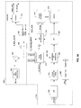
- FIG. 3A is a diagram of an exemplary OFDM timing acquisition and tracking system, in accordance with an embodiment of the invention.
- FIG. 3B is a diagram illustrating phase offsets for exemplary timing offsets, in accordance with various embodiments of the invention.
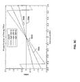
- FIG. 3C is a diagram illustrating phase offsets for exemplary timing offsets by subcarrier, in accordance with various embodiments of the invention.
- FIG. 4 is a flow chart illustrating an exemplary timing acquisition and tracking process, in accordance with an embodiment of the invention.
- Certain embodiments of the invention may be found in a method and system for RS timing loop for OFDM symbol synchronization and tracking.
- Aspects of the method and system for a reference signal (RS) timing loop for OFDM symbol synchronization and tracking may comprise tracking symbol timing in an Orthogonal Frequency Division Multiplexing (OFDM) signal based on at least a reference symbol set.
- a receiver timing may be adjusted based on at least the symbol timing.
- OFDM Orthogonal Frequency Division Multiplexing
- the symbol timing may be tracked by generating an output signal as a function of a guard time ⁇ t g in a phase discrimination feedback loop.
- the reference symbol (RS) set may be generated in an RS extraction module or circuit, from at least a fast Fourier transform of the received OFDM signal.
- the receiver timing may be coarsely adjusted and then finely adjusted.
- the coarse receiver timing adjustment may be achieved based on processing at least a primary synchronization signal and a secondary synchronization signal.
- the reference symbol set may comprise a plurality of time-frequency slots.
- the plurality of time-frequency slots may change according to a frequency shift and PN sequence that may modulate the reference symbols.
- the PN generated sequences may be determined by base station identifier.
- This base station identifier may be determined by the primary synchronization signal (PSS) and secondary synchronization signal (SSS).
- the OFDM signal may conform to a Universal Mobile Telecommunications Standards (UMTS) long-term evolution (LTE) signal.
- UMTS Universal Mobile Telecommunications Standards
- LTE long-term evolution
- the adjustment of the receiver timing may be controlled via a receiver timing generator.
- FIG. 1A is a diagram illustrating exemplary cellular multipath communication between a base station and a mobile computing terminal, in connection with an embodiment of the invention.
- a building 140 such as a house or office
- a mobile terminal 142 a factory 124
- a base station 126 a base station 126
- the base station 126 and the mobile terminal 142 may comprise suitable logic, circuitry and/or code that may be enabled to generate and process MIMO communication signals.
- Wireless communications between the base station 126 and the mobile terminal 142 may take place over a wireless channel.
- the wireless channel may comprise a plurality of communication paths, for example, the communication paths 130, 132 and 134.
- the wireless channel may change dynamically as the mobile terminal 142 and/or the car 128 moves.
- the mobile terminal 142 may be in line-of-sight (LOS) of the base station 126.
- LOS line-of-sight
- the radio signals may travel as reflected communication paths between the communicating entities, as illustrated by the exemplary communication paths 130, 132 and 134.
- the radio signals may be reflected by man-made structures like the building 140, the factory 124 or the car 128, or by natural obstacles like hills. Such a system may be referred to as a non-line-of-sight (NLOS) communications system.
- NLOS non-line-of-sight
- Signals communication by the communication system may comprise both LOS and NLOS signal components. If a LOS signal component is present, it may be much stronger than NLOS signal components. In some communication systems, the NLOS signal components may create interference and reduce the receiver performance. This may be referred to as multipath interference.
- the communication paths 130, 132 and 134 may arrive with different delays at the mobile terminal 142.
- the communication paths 130, 132 and 134 may also be differently attenuated.
- the received signal at the mobile terminal 142 may be the sum of differently attenuated communication paths 130, 132 and/or 134 that may not be synchronized and that may dynamically change. Such a channel may be referred to as a fading multipath channel.
- a fading multipath channel may introduce interference but it may also introduce diversity and degrees of freedom into the wireless channel.
- Communication systems with multiple antennas at the base station and/or at the mobile terminal for example MIMO systems, may be particularly suited to exploit the characteristics of wireless channels and may extract large performance gains from a fading multipath channel that may result in significantly increased performance with respect to a communication system with a single antenna at the base station 126 and at the mobile terminal 142, in particular for NLOS signals.
- OFDM Orthogonal Frequency Division Multiplexing
- FIG. 1B is a diagram illustrating an exemplary MIMO communication system, in accordance with an embodiment of the invention.
- a MIMO transmitter 102 and a MIMO receiver 104, and antennas 106, 108, 110, 112, 114 and 116.
- the MIMO transmitter 102 may comprise a processor block 118, a memory block 120, and a signal processing block 122.
- the MIMO receiver 104 may comprise a processor block 124, a memory block 126, and a signal processing block 128.
- a wireless channel comprising communication paths h11, h 12 , h 22 , h 21 , h 2 NTX , h 1 NTX , h NRX 1 , h NRX 2 , h NRX NTX , where h mn may represent a channel coefficient from transmit antenna n to receiver antenna m.
- transmit symbols x 1 , x 2 and x NTX receive symbols y 1 , y 2 and Y NRX .
- the MIMO transmitter 102 may comprise suitable logic, circuitry and/or code that may be enabled to generate transmit symbols x i i ⁇ ⁇ 1,2,... N TX ⁇ that may be transmitted by the transmit antennas, of which the antennas 106, 108 and 110 may be depicted in FIG. 1B .
- the processor block 118 may comprise suitable logic, circuitry, and/or code that may be enabled to process signals.
- the memory block 120 may comprise suitable logic, circuitry, and/or code that may be enabled to store and/or retrieve information for processing in the MIMO transmitter 102.
- the signal processing block 122 may comprise suitable logic, circuitry and/or code that may be enabled to process signals, for example in accordance with one or more MIMO transmission protocols.
- the MIMO receiver 104 may comprise suitable logic, circuitry and/or code that may be enabled to process the receive symbols y i i ⁇ ⁇ 1,2,... N RX ⁇ that may be received by the receive antennas, of which the antennas 112, 114 and 116 may be shown in FIG. 1B .
- the processor block 124 may comprise suitable logic, circuitry, and/or code that may be enabled to process signals.
- the memory block 126 may comprise suitable logic, circuitry, and/or code that may be enabled to store and/or retrieve information for processing in the MIMO receiver 104.
- the signal processing block 128 may comprise suitable logic, circuitry and/or code that may be enabled to process signals, for example in accordance with one or more MIMO protocols.
- y Hx + n
- y [ y 1 , y 2 ,... y NRX ]
- T may be a column vector with N RX elements, .
- T may denote a vector transpose
- x [ x 1 , x 2 ,... x NTX ]
- T is a column vector with N TX elements and
- n is a column vector of noise samples with N RX elements.
- the system diagram in FIG. 1B may illustrate an exemplary multi-antenna system as it may be utilized in a Universal Mobile Telecommunication System (UMTS) Long-Term Evolution (LTE) system.
- UMTS Universal Mobile Telecommunication System
- LTE Long-Term Evolution
- a symbol stream, for example x 1 ( t ) over antenna 106 may be transmitted.
- a symbol stream, for example x 1 ( t ) may comprise one or more symbols, wherein each symbol may be modulated onto a different sub-carrier.
- OFDM systems may generally use a relatively large number of subcarriers in parallel, for each symbol stream.
- a symbol stream x 1 ( t ) may comprise symbols on carriers f m : m ⁇ ⁇ 1, 2,...
- M ⁇ , and M may be a subset of the FFT size that may be utilized at the receiver. For instance, with FFT sizes of N , M ⁇ N and may create guard-tones that may allow utilization of variable bandwidth when deployed.
- the M sub-carriers may comprise a symbol stream x 1 ( t ), for example, that may occupy a bandwidth of a few kilohertz to a few megahertz. Common bandwidth may be between 1 MHz and up to 100 MHz, for example.
- each symbol stream may comprise one or more sub-carriers, and for each sub-carrier a wireless channel may comprise multiple transmission paths.
- a wireless channel h 12 from transmit antenna 108 to receive antenna 112, as illustrated in the figure, may be multi-dimensional.
- the wireless channel h 12 may comprise a temporal impulse response, comprising one or more multipath components.
- the wireless channel h 12 may also comprise a different temporal impulse response for each sub-carrier f m of the symbol stream, for example x 2 ( t ).
- the wireless channels as illustrated in FIG. 1B depict a spatial dimension of the wireless channel because the transmitted signal from each transmit antenna may be received differently at each receiver antenna.
- a channel impulse response may be measured and/or estimated for each sub-carrier.
- FIG. 2 is an illustration of an exemplary OFDM symbol stream, in accordance with an embodiment of the invention.
- a time axis 210 a time domain symbol 0 comprising a cyclic prefix CP(0) 202a, an Inverse Fast Fourier Transform (IFFT) symbol less CP(0) (IFFT(0)) 202b, and a cyclic prefix CP(0) 202c;
- a time domain symbol 1 comprising a cyclic prefix CP(1) 204a, an IFFT symbol less CP(1) (IFFT(0)) 204b, and a cyclic prefix CP(1) 204c.
- the IFFT(0) 202b and the CP(0) 202c may together form a complete IFFT symbol for time domain symbol 0.
- the CP(0) 202a may be substantially similar to CP(0) 202c.
- the IFFT(1) 204b and the CP(1) 204c may together form a complete IFFT symbol for time domain symbol 1, and CP(1) 202a may be substantially similar to CP(1) 202c.
- An LTE slot structure for example, may comprise 3, 6, or 7 OFDM symbols per slot (two of which may be illustrated in FIG. 2 ).
- an output of an IFFT comprising of IFFT(0) 202b and CP(0) 202c may be used to generate CP(0) 202a from CP(0) 202c, and append it to IFFT(0) 202b.
- the cyclic prefix CP(0) 202 may be utilized to avoid inter-symbol interference at an OFDM receiver, in the presence of multi-path propagation in the wireless channel.
- a sampled input signal may be processed for each received symbol, for example over an FFT input window 206.
- the FFT input window 206 may be located in a time domain symbol time slot, for example in time domain symbol 0.
- the FFT input window 206 may not extend into a neighboring symbol, to avoid inter-symbol interference.
- the slot marker may indicate the beginning of a slot, for example time domain symbol slot 0, as illustrated in FIG. 2 .
- the slot marker 208 together with ⁇ t g may define the position of the FFT input window 206 within a symbol slot. In most instances, to keep interference due to the multipath channel as low as possible at the receiver, it may be desirable to keep ⁇ t g small.
- Symbol timing may be acquired by a timing acquisition and tracking system, which may exploit reference signals (RS) embedded in an OFDM signal.
- Reference symbols may be known symbols that may be transmitted according to a known pattern over the time, frequency and spatial resources in an OFDM system. In other words, reference symbols may be transmitted at known timing instances, on known OFDM carriers over certain antennas.
- the receiver may determine correct timing information, for example, through coherent demodulation.
- RS symbols may be transmitted from each antenna in a multiple antenna OFDM system.
- RS symbols may be generated based on cell-specific hopping pattern, and may comprise pseudo-noise (PN) covered sequences of Reference symbols.
- PN pseudo-noise
- the RS tone spacing may be 6 carriers, per transmit antenna, for example.
- the RS tone spacing may be 2, or 4 carriers, for example.
- the RS sequence may not be known to the mobile terminal (user equipment, UE) during initial acquisition, for example through the synchronization signals.
- the UE may have obtained the cell-specific hopping pattern for the RS symbols, and the PN covering sequence.
- the RS symbols may then be decoded in a timing acquisition and tracking block to provide fine timing and tracking.
- UMTS Universal Mobile Telecommunication System
- LTE Long-term evolution
- the three step process may comprise: a) recovering slot timing from the PSS; b) recovering frame timing from the SSS; and c) obtaining an estimation of estimation of timing offset and tracking from the RS symbols.
- FIG. 3A is a diagram of an exemplary OFDM timing acquisition and tracking system, in accordance with an embodiment of the invention.
- the timing part 340 may comprise an RS phase discriminator 302, an adder 304, a delay block 306, an integrator 308, and a threshold block 310.
- the common receiver part 342 may comprise a timing generator 312, an RS extraction module or circuit 314, a channel estimation block 316, a receiver operations block (RXCVR) 318, a fast Fourier transform (FFT) block 320, a buffering block 330, a sampling bandwidth (BW) filter 332, and an analog-to-digital block 334.
- a timing generator 312 an RS extraction module or circuit 314, a channel estimation block 316, a receiver operations block (RXCVR) 318, a fast Fourier transform (FFT) block 320, a buffering block 330, a sampling bandwidth (BW) filter 332, and an analog-to-digital block 334.
- RXCVR receiver operations block
- FFT fast Fourier transform
- BW sampling bandwidth
- the timing part 340 may comprise suitable logic, circuitry and/or code that may be enabled to extract timing information by processing an RS set of signals, which may generate an output to_accum that may control the timing generator 312, for example.
- the RS phase discriminator 302 may comprise suitable logic, circuitry and/or code that may be enabled to compare the timing of the RS set input signal with, for example, an input clock signal and may generate an error signal e k .
- the adder 304 may comprise suitable logic, circuitry and/or code that may be enabled to generate a weighted sum signal at its output, from a plurality of inputs.
- the delay block 306 may comprise suitable logic, circuitry and/or code that may be enabled to delay an input signal by a certain time interval, for example one or more sample periods.
- the delay block 306 may comprise suitable logic, circuitry and/or code that may be enabled to delay an input signal by a certain time interval, for example one or more sample periods.
- the integrator 308 may comprise suitable logic, circuitry and/or code that may be enabled to generate an output that may be the integration of one or more input signals, and the integrator 308 may be reset by the reset_cntrl signal.
- the threshold block 310 may comprise suitable logic, circuitry and/or code that may be enabled to compare a threshold input signal with the tt_loop_accum input signal, and generate output signals reset_cntrl and to_accum. For example, when the tt_loop_accum signal may exceed the threshold level, the reset_cntrl signal may activate and reset, for example, the integrator 308.
- the common receiver part 342 may comprise suitable logic, circuitry and/or code that may be enabled to receive radio frequency signals, and process these signals.
- the processing may comprise FFT computation, RS symbol extraction, channel estimation and other receiver signal processing.
- the timing generator 312 may comprise suitable logic, circuitry and/or code that may be enabled to generate timing signals for RS extraction, rs_strb, and slot timing, slot_strb.
- the signal slot_strb may be used to control FFT timing in the buffering block 330, for example.
- the module or circuit 314 may comprise suitable logic, circuitry and/or code that may be enabled to extract the RS symbols from the FFT module or circuit 320 output.
- the channel estimation module or circuit 316 may comprise suitable logic, circuitry and/or code that may be enabled to estimate the wireless channel response for RS symbols, which may be desirable for receiver operations.
- the receiver operations module or circuit (RXCVR) 318 may comprise suitable logic, circuitry and/or code that may be enabled to measure and/or verify performance during receiver operations.
- the fast Fourier-transform (FFT) module or circuit 320 may comprise suitable logic, circuitry and/or code that may be enabled to generate a Fast Fourier Transform for an input signal.
- the buffering module or circuit 330 may comprise suitable logic, circuitry and/or code that may be enabled to interface with, for example, the FFT engine.
- the buffering module or circuit 330 may assist in, for example, dedicated processes, measurement processes, multimedia broadcast multicast services (MBMS), and/or SSS processing for hopping pattern determination. In some instances, each of the processes may be performed in parallel.
- the sample BW filter 332 may comprise suitable logic, circuitry and/or code that may be enabled to filter the signal at its input, and generate an output signal with limited bandwidth.
- the analog-to-digital (A2D) module or circuit 334 may comprise suitable logic, circuitry and/or code that may be enabled to receive an analog RF-filtered signal and convert it to a digital signal representation at the output, with an arbitrary number of bits.
- the master timer 336 may comprise suitable logic, circuitry and/or code that may be enabled to provide basic timing functionality in the receiver. In some instances, the master timer 336 may count over 10 ms periods, and may be clocked at 30.72 MHz, for example.
- the master timer 336 may comprise a slot counter, and a sample counter.
- the input to the master timer 336 may be provided by an operating RF crystal, referred to as a TXCO, for example.
- the common receiver part 342 may receive radio frequency signals, and process these signals. Processing may comprise FFT computation, RS symbol extraction, channel estimation and other receiver signal processing. Some timing aspects of the common receiver part 342 may be controlled by the timing part 340. For example, the symbol timing on one or more receiver subcarrier/carrier frequency, for example f1 and/or f2 as illustrated in FIG. 2 , may be determined.
- the RS phase discriminator 302 may receive at its input, a set of RS symbols, which may be extracted in the RS extraction module or circuit 314 to determine timing information about the RS carrying-carrier.
- the output of the RS phase discriminator 302 may be communicatively coupled to a first input of the adder 304.
- a second input of the adder 304 may be coupled to the output of the delay module or circuit 306, and the output of the adder 304 may be a weighted sum of its inputs.
- the delay module or circuit 306 may delay an input signal by a certain time interval, for example one or more sample periods.
- the delay module or circuit 306 may provide appropriate delay for the feedback signal provided to the adder 304 from the integrator 308.
- An output of the adder 304, tt_loop_accum may be communicatively coupled to a first input of the threshold module or circuit 310, and a first input of the integrator 308.
- a second input of the threshold module or circuit 310 may be coupled to a threshold-level defining signal.
- the threshold module or circuit 310 may compare a threshold signal with the tt_loop_accum signal, and generate output signals reset_cntrl and to_accum. For example, when the tt_loop_accum signal may exceed the threshold level, the reset_cntrl signal may activate and reset, for example, the integrator 308.
- the to_accum signal may increase at a rate that is a function of ⁇ t , and may thus allow information about ⁇ t to be communicated to, for example, the timing generator 312, which in turn may control the FFT input window's position in the time domain.
- a second input to the integrator 308 may be set to a known, constant level, for example zero.
- the integrator 308 may integrate one or more input signals, and the integrator 308 may be reset by the reset_cntrl signal.
- the analog-to-digital (A2D) module or circuit 334 may receive an analog RF-filtered signal and convert it to a digital signal representation at the output, with an arbitrary number of bits.
- the A2D 334 output may be communicatively coupled to an input of the sample BW filter 332.
- the sample BW filter 332 may filter the signal at its input, and generate an output signal with limited bandwidth and/or attenuate certain frequency bands.
- the output of the sample BW filter 332 may be communicatively coupled to a first input of the buffering module or circuit 330.
- a second input to the buffering module or circuit 330 may be communicatively coupled to the output signal slot_strb from the timing generator 312.
- the buffering module or circuit 330 may interface with, for example, the FFT engine.
- the buffering module or circuit 330 may assist in dedicated processes, measurement processes, multimedia broadcast multicast services (MBMS), and/or SSS processing for RS PN sequence determination. In some instances, each of the processes may be performed in parallel.
- the output of the buffering module or circuit 330 may be communicatively coupled to the FFT module or circuit 320.
- the FFT module or circuit 320 may generate a Fast Fourier Transform for an input signal communicatively coupled from the buffering module or circuit 330. Similar to the buffering module or circuit 330, the FFT module or circuit 320 may assist in signal processing for dedicated processes, measurement processes, multimedia broadcast multicast services (MBMS), and/or SSS processing for radio time framing and RS PN sequence determination.
- a first output of the FFT module or circuit 320 may be communicatively coupled to a first input of the RS extraction module or circuit 314.
- the RS extraction module or circuit 314 may extract the RS symbols from the FFT module or circuit 320 output.
- a generated hopping sequence from the demodulated base station signal and/or pseudo-noise (PN) covering for RS decoding.
- the RS symbols extracted and output at the RS extraction module or circuit 314 may be communicatively coupled to the input of the timing part 340, and a channel estimation module or circuit 316.
- the hopping pattern may be fed to the RS extraction module or circuit 314 via the rs_hopping_pattern signal on a second input, as illustrated in FIG. 3A .
- the RS extraction module or circuit 314 timing may be controlled via a third input signal rs_strb, communicatively coupled to an output of the timing generator 312.
- the timing generator 312 may generate timing signal for RS extraction, rs_strb, and slot timing, slot_strb.
- the signal slot_strb may be used to control FFT timing in the buffering module or circuit 330.
- the timing generator 312 may generate the output timing signals for timing corrections and tracking.
- the master timer input signal may be communicatively coupled to the master timer 336 output.
- the master timer 336 may provide basic timing functionality in the receiver. In some instances, the master timer 336 may count over 10 ms periods, and may be clocked at 30.72 MHz, for example.
- the master timer 336 may comprise a slot counter, and a sample counter.
- the input to the master timer 336 may be provided by an operating RF crystal, a temperature-controlled crystal oscillator (TXCO), for example.
- TXCO temperature-controlled crystal oscillator
- the channel estimation module or circuit 316 may estimate the wireless channel response for RS symbols, which may be desirable for receiver operations.
- the channel estimation output may be communicatively coupled to the RXCVR 318.
- the RXCVR 318 may measure and/or verify receiver performance functionality.
- FIG. 3B is a diagram illustrating phase offsets for exemplary timing offsets, in accordance with various embodiments of the invention.
- From PSS and SSS slot markers may be obtained for the received signal to within the bandwidth of the PSS processing, for example.
- the Cyclic Prefix CP
- CP Cyclic Prefix
- ⁇ t g the value of ⁇ t g to avoid that the sampled input to FFT processing may comprise adjacent symbols (intersymbol interference - ISI) as this may degrade performance.
- ⁇ t g may be tracked, and may provide guard against timing shifts due to mobility, for example.
- a timing offset may be manifested by a growing phase offset when indexed by tone frequency.
- hrx k z k ⁇ h k + n k
- timing offset may introduce linearly decreasing phase as a function of frequency.
- FIG. 3C is a diagram illustrating phase offsets for exemplary timing offsets by subcarrier, in accordance with various embodiments of the invention.
- timing offset may manifest phase offset across the bandwidth of the channel, as illustrated for a plurality of subcarriers by the plots 352a - 352d.
- the slope of the phase offset in function of the frequency may be linear with a positive slope for early sampled FFT, and a negative slope for late sampled FFTs, for example.
- FIG. 4 is a flow chart illustrating an exemplary timing acquisition and tracking process, in accordance with an embodiment of the invention.
- the primary and secondary synchronization signals, (PSS) and (SSS) may be decoded in step 404.
- the decoding of the PSS and SSS may provide coarse timing information for frame and slot synchronization, for example.
- the FFT block 320 for example, may generate an FFT of a received signal.
- the RS extraction block 314 for example, may extract an RS set in the RS extraction block 314. This RS set may be fed to the timing part 340.
- the timing part 340 may track ⁇ t g using the feedback loop depicted in FIG. 3A .
- the to_accum output signal from the threshold block 310 may carry information about ⁇ t g to the timing generator 312.
- the output signal to_accum may enable tracking of the symbol timing, and adjust the timing of the receiver, for example in the timing generator 312.
- the timing generator 312 may adjust the timing based on the input signal to_accum.
- the adjusted and tracked timing may be communicatively coupled from the timing generator 312 to the buffering block 330, where the timing of the FFT input window may be adjusted correspondingly.
- a method and system for a RS timing loop for OFDM symbol synchronization and tracking may comprise tracking symbol timing in an Orthogonal Frequency Division Multiplexing (OFDM) signal based on at least a reference symbol set, as described for FIG. 2 and FIG. 3A .
- a receiver timing, as described for FIG. 2 and FIG. 3A may be adjusted based on at least the symbol timing.
- the symbol timing may be tracked by generating an output signal as a function of a guard time ⁇ t g in a phase discrimination feedback loop, for example timing part 340.
- the reference symbol (RS) set may be generated in an RS extraction module or circuit 314, from at least a fast Fourier transform of the received OFDM signal.
- the receiver timing may be coarsely adjusted and then finely adjusted, for example.
- the coarse receiver timing adjustment may be based on processing at least a primary synchronization signal and a secondary synchronization signal, as described for FIG. 3A .
- the reference symbol set may comprise a plurality of time-frequency slots.
- the plurality of time-frequency slots may change according to a frequency shift and pseudo-noise sequence that modulates the reference symbols.
- the OFDM signal may conform to a Universal Mobile Telecommunications Standards (UMTS) long-term evolution (LTE) signal.
- UMTS Universal Mobile Telecommunications Standards
- LTE long-term evolution
- the adjustment of the receiver timing may be controlled via a
- Another embodiment of the invention may provide a machine-readable and/or computer-readable storage and/or medium, having stored thereon, a machine code and/or a computer program having at least one code section executable by a machine and/or a computer, thereby causing the machine and/or computer to perform the steps as described herein for a method and system for a reference signal (RS) timing loop for OFDM symbol synchronization and tracking.
- RS reference signal
- the present invention may be realized in hardware, software, or a combination of hardware and software.
- the present invention may be realized in a centralized fashion in at least one computer system, or in a distributed fashion where different elements are spread across several interconnected computer systems. Any kind of computer system or other apparatus adapted for carrying out the methods described herein is suited.
- a typical combination of hardware and software may be a general-purpose computer system with a computer program that, when being loaded and executed, controls the computer system such that it carries out the methods described herein.
- the present invention may also be embedded in a computer program product, which comprises all the features enabling the implementation of the methods described herein, and which when loaded in a computer system is able to carry out these methods.
- Computer program in the present context means any expression, in any language, code or notation, of a set of instructions intended to cause a system having an information processing capability to perform a particular function either directly or after either or both of the following: a) conversion to another language, code or notation; b) reproduction in a different material form.
Landscapes
- Engineering & Computer Science (AREA)
- Computer Networks & Wireless Communication (AREA)
- Signal Processing (AREA)
- Mobile Radio Communication Systems (AREA)
- Synchronisation In Digital Transmission Systems (AREA)
Abstract
Description
- This application makes reference to:
- United States Application Serial No. _(Attorney Docket No. 18899US01), filed on even date herewith; and
- United States Application Serial No. _(Attorney Docket No. 18901US01), filed on even date herewith.
- Each of the above referenced applications is hereby incorporated herein by reference in its entirety.
- Certain embodiments of the invention relate to signal processing for communication systems. More specifically, certain embodiments of the invention relate to a method and system for a reference signal (RS) timing loop for OFDM symbol synchronization and tracking.
- Mobile communications have changed the way people communicate and mobile phones have been transformed from a luxury item to an essential part of every day life. The use of mobile phones is today dictated by social situations, rather than hampered by location or technology. While voice connections fulfill the basic need to communicate, and mobile voice connections continue to filter even further into the fabric of every day life, the mobile Internet is the next step in the mobile communication revolution. The mobile Internet is poised to become a common source of everyday information, and easy, versatile mobile access to this data will be taken for granted.
- Third generation (3G) cellular networks have been specifically designed to fulfill these future demands of the mobile Internet. As these services grow in popularity and usage, factors such as cost efficient optimization of network capacity and quality of service (QoS) will become even more essential to cellular operators than it is today. These factors may be achieved with careful network planning and operation, improvements in transmission methods, and advances in receiver techniques. To this end, carriers need technologies that will allow them to increase throughput and, in turn, offer advanced QoS capabilities and speeds that rival those delivered by cable modem and/or DSL service providers. Recently, advances in multiple antenna technology and other physical layer technologies have started to significantly increase available communications data rates.
- Further limitations and disadvantages of conventional and traditional approaches will become apparent to one of skill in the art, through comparison of such systems with some aspects of the present invention as set forth in the remainder of the present application with reference to the drawings.
- A method and/or system for reference signal (RS) timing loop for OFDM symbol synchronization and tracking, substantially as shown in and/or described in connection with at least one of the figures, as set forth more completely in the claims.
According to an aspect, a method for processing communication signals comprises: - tracking symbol timing in an Orthogonal Frequency Division Multiplexing (OFDM) signal based on at least a reference symbol set; and
- adjusting receiver timing based on at least said symbol timing.
- one or more circuits in a receiver operable to, at least:
- track symbol timing in an Orthogonal Frequency Division Multiplexing (OFDM) signal, wherein said tracking is based on at least a reference symbol set; and
- adjust receiver timing based on at least said symbol timing.
- These and other advantages, aspects and novel features of the present invention, as well as details of an illustrated embodiment thereof, will be more fully understood from the following description and drawings.
-
FIG. 1A is a diagram illustrating exemplary cellular multipath communication between a base station and a mobile computing terminal, in connection with an embodiment of the invention. -
FIG. 1B is a diagram illustrating an exemplary MIMO communication system, in accordance with an embodiment of the invention. -
FIG. 2 is a diagram illustrating an exemplary OFDM symbol stream, in accordance with an embodiment of the invention. -
FIG. 3A is a diagram of an exemplary OFDM timing acquisition and tracking system, in accordance with an embodiment of the invention. -
FIG. 3B is a diagram illustrating phase offsets for exemplary timing offsets, in accordance with various embodiments of the invention. -
FIG. 3C is a diagram illustrating phase offsets for exemplary timing offsets by subcarrier, in accordance with various embodiments of the invention. -
FIG. 4 is a flow chart illustrating an exemplary timing acquisition and tracking process, in accordance with an embodiment of the invention. - Certain embodiments of the invention may be found in a method and system for RS timing loop for OFDM symbol synchronization and tracking. Aspects of the method and system for a reference signal (RS) timing loop for OFDM symbol synchronization and tracking may comprise tracking symbol timing in an Orthogonal Frequency Division Multiplexing (OFDM) signal based on at least a reference symbol set. A receiver timing may be adjusted based on at least the symbol timing.
- The symbol timing may be tracked by generating an output signal as a function of a guard time Δtg in a phase discrimination feedback loop. The reference symbol (RS) set may be generated in an RS extraction module or circuit, from at least a fast Fourier transform of the received OFDM signal. The receiver timing may be coarsely adjusted and then finely adjusted. The coarse receiver timing adjustment may be achieved based on processing at least a primary synchronization signal and a secondary synchronization signal. The reference symbol set may comprise a plurality of time-frequency slots. The plurality of time-frequency slots may change according to a frequency shift and PN sequence that may modulate the reference symbols. The PN generated sequences may be determined by base station identifier. This base station identifier may be determined by the primary synchronization signal (PSS) and secondary synchronization signal (SSS). The OFDM signal may conform to a Universal Mobile Telecommunications Standards (UMTS) long-term evolution (LTE) signal. The adjustment of the receiver timing may be controlled via a receiver timing generator.
-
FIG. 1A is a diagram illustrating exemplary cellular multipath communication between a base station and a mobile computing terminal, in connection with an embodiment of the invention. Referring toFIG. 1A , there is shown abuilding 140 such as a house or office, amobile terminal 142, afactory 124, abase station 126, acar 128, andcommunication paths - The
base station 126 and themobile terminal 142 may comprise suitable logic, circuitry and/or code that may be enabled to generate and process MIMO communication signals. - Wireless communications between the
base station 126 and themobile terminal 142 may take place over a wireless channel. The wireless channel may comprise a plurality of communication paths, for example, thecommunication paths mobile terminal 142 and/or thecar 128 moves. In some cases, themobile terminal 142 may be in line-of-sight (LOS) of thebase station 126. In other instances, there may not be a direct line-of-sight between themobile terminal 142 and thebase station 126 and the radio signals may travel as reflected communication paths between the communicating entities, as illustrated by theexemplary communication paths building 140, thefactory 124 or thecar 128, or by natural obstacles like hills. Such a system may be referred to as a non-line-of-sight (NLOS) communications system. - Signals communication by the communication system may comprise both LOS and NLOS signal components. If a LOS signal component is present, it may be much stronger than NLOS signal components. In some communication systems, the NLOS signal components may create interference and reduce the receiver performance. This may be referred to as multipath interference. The
communication paths mobile terminal 142. Thecommunication paths mobile terminal 142 may be the sum of differently attenuatedcommunication paths - A fading multipath channel may introduce interference but it may also introduce diversity and degrees of freedom into the wireless channel. Communication systems with multiple antennas at the base station and/or at the mobile terminal, for example MIMO systems, may be particularly suited to exploit the characteristics of wireless channels and may extract large performance gains from a fading multipath channel that may result in significantly increased performance with respect to a communication system with a single antenna at the
base station 126 and at themobile terminal 142, in particular for NLOS signals. Furthermore, Orthogonal Frequency Division Multiplexing (OFDM) systems may be suitable for wireless systems with multipath. -
FIG. 1B is a diagram illustrating an exemplary MIMO communication system, in accordance with an embodiment of the invention. Referring toFIG. 1B , there is shown aMIMO transmitter 102 and aMIMO receiver 104, andantennas MIMO transmitter 102 may comprise aprocessor block 118, amemory block 120, and asignal processing block 122. TheMIMO receiver 104 may comprise aprocessor block 124, amemory block 126, and asignal processing block 128. There is also shown a wireless channel comprising communication paths h11, h12, h22, h21, h2 NTX, h1 NTX, hNRX 1, hNRX 2, hNRX NTX, where hmn may represent a channel coefficient from transmit antenna n to receiver antenna m. There may be NTX transmitter antennas and NRX receiver antennas. There is also shown transmit symbols x1, x2 and xNTX, and receive symbols y1, y2 and YNRX. - The
MIMO transmitter 102 may comprise suitable logic, circuitry and/or code that may be enabled to generate transmit symbols xi i ∈ {1,2,...NTX } that may be transmitted by the transmit antennas, of which theantennas FIG. 1B . Theprocessor block 118 may comprise suitable logic, circuitry, and/or code that may be enabled to process signals. Thememory block 120 may comprise suitable logic, circuitry, and/or code that may be enabled to store and/or retrieve information for processing in theMIMO transmitter 102. Thesignal processing block 122 may comprise suitable logic, circuitry and/or code that may be enabled to process signals, for example in accordance with one or more MIMO transmission protocols. TheMIMO receiver 104 may comprise suitable logic, circuitry and/or code that may be enabled to process the receive symbols yi i ∈ {1,2,...NRX } that may be received by the receive antennas, of which theantennas FIG. 1B . Theprocessor block 124 may comprise suitable logic, circuitry, and/or code that may be enabled to process signals. Thememory block 126 may comprise suitable logic, circuitry, and/or code that may be enabled to store and/or retrieve information for processing in theMIMO receiver 104. Thesignal processing block 128 may comprise suitable logic, circuitry and/or code that may be enabled to process signals, for example in accordance with one or more MIMO protocols. An input-output relationship between the transmitted and the received signal in a MIMO system may be written as:
where y = [y 1,y 2,...yNRX ] T may be a column vector with NRX elements, .T may denote a vector transpose, H = [hij ] : i ∈ {1,2,...NRX }; j ∈ {1,2,...NTX } may be a channel matrix of dimensions NRX by NTX, x = [x 1,x 2,...xNTX ] T is a column vector with NTX elements and n is a column vector of noise samples with NRX elements. - The system diagram in
FIG. 1B may illustrate an exemplary multi-antenna system as it may be utilized in a Universal Mobile Telecommunication System (UMTS) Long-Term Evolution (LTE) system. Over each of the NTX transmit antennas, a symbol stream, for example x 1(t) overantenna 106, may be transmitted. A symbol stream, for example x 1(t), may comprise one or more symbols, wherein each symbol may be modulated onto a different sub-carrier. OFDM systems may generally use a relatively large number of subcarriers in parallel, for each symbol stream. For example, a symbol stream x 1(t) may comprise symbols on carriers fm : m ∈ {1, 2,...M}, and M may be a subset of the FFT size that may be utilized at the receiver. For instance, with FFT sizes of N, M < N and may create guard-tones that may allow utilization of variable bandwidth when deployed. The M sub-carriers may comprise a symbol stream x 1(t), for example, that may occupy a bandwidth of a few kilohertz to a few megahertz. Common bandwidth may be between 1 MHz and up to 100 MHz, for example. Thus, each symbol stream may comprise one or more sub-carriers, and for each sub-carrier a wireless channel may comprise multiple transmission paths. For example, a wireless channel h 12 from transmitantenna 108 to receiveantenna 112, as illustrated in the figure, may be multi-dimensional. In particular, the wireless channel h 12 may comprise a temporal impulse response, comprising one or more multipath components. The wireless channel h 12 may also comprise a different temporal impulse response for each sub-carrier fm of the symbol stream, for example x 2(t). Finally, the wireless channels as illustrated inFIG. 1B depict a spatial dimension of the wireless channel because the transmitted signal from each transmit antenna may be received differently at each receiver antenna. Thus, a channel impulse response may be measured and/or estimated for each sub-carrier. -
FIG. 2 is an illustration of an exemplary OFDM symbol stream, in accordance with an embodiment of the invention. Referring toFIG. 2 , there is shown atime axis 210; atime domain symbol 0 comprising a cyclic prefix CP(0) 202a, an Inverse Fast Fourier Transform (IFFT) symbol less CP(0) (IFFT(0)) 202b, and a cyclic prefix CP(0) 202c; atime domain symbol 1 comprising a cyclic prefix CP(1) 204a, an IFFT symbol less CP(1) (IFFT(0)) 204b, and a cyclic prefix CP(1) 204c. The IFFT(0) 202b and the CP(0) 202c may together form a complete IFFT symbol fortime domain symbol 0. The CP(0) 202a may be substantially similar to CP(0) 202c. Similarly, the IFFT(1) 204b and the CP(1) 204c may together form a complete IFFT symbol fortime domain symbol 1, and CP(1) 202a may be substantially similar to CP(1) 202c. There is also shown anFFT input window 206, a guard time Δtg , and aslot marker 208. An LTE slot structure, for example, may comprise 3, 6, or 7 OFDM symbols per slot (two of which may be illustrated inFIG. 2 ). - To generate an Orthogonal Frequency Division Multiplexing (OFDM) symbol, an output of an IFFT comprising of IFFT(0) 202b and CP(0) 202c may be used to generate CP(0) 202a from CP(0) 202c, and append it to IFFT(0) 202b. The cyclic prefix CP(0) 202 may be utilized to avoid inter-symbol interference at an OFDM receiver, in the presence of multi-path propagation in the wireless channel.
- At an OFDM receiver, for
example MIMO receiver 104, a sampled input signal may be processed for each received symbol, for example over anFFT input window 206. In order to decode the received symbols, it may be desirable that theFFT input window 206 may be located in a time domain symbol time slot, for example intime domain symbol 0. In particular, it may be desirable that theFFT input window 206 may not extend into a neighboring symbol, to avoid inter-symbol interference. Thus, the slot marker may indicate the beginning of a slot, for example timedomain symbol slot 0, as illustrated inFIG. 2 . Theslot marker 208 together with Δtg may define the position of theFFT input window 206 within a symbol slot. In most instances, to keep interference due to the multipath channel as low as possible at the receiver, it may be desirable to keep Δtg small. - Thus, it may be desirable to acquire symbol level timing, and maintain it as it may drift, for example, because of changes in propagation due to mobility. In some instances, this may be combined with other timing level acquisition and tracking, for example frame synchronization. In many instances, synchronization via the Primary Synchronization Signal (PSS) and the Secondary Synchronization Signal (SSS) may be obtained by other means. Symbol timing may be acquired by a timing acquisition and tracking system, which may exploit reference signals (RS) embedded in an OFDM signal. Reference symbols may be known symbols that may be transmitted according to a known pattern over the time, frequency and spatial resources in an OFDM system. In other words, reference symbols may be transmitted at known timing instances, on known OFDM carriers over certain antennas. By decoding and processing RS symbols, the receiver may determine correct timing information, for example, through coherent demodulation. RS symbols may be transmitted from each antenna in a multiple antenna OFDM system.
- In the Enhanced Universal Terrestrial Radio Access (EUTRA) interface, RS symbols may be generated based on cell-specific hopping pattern, and may comprise pseudo-noise (PN) covered sequences of Reference symbols. In accordance with an embodiment of the invention, the RS tone spacing may be 6 carriers, per transmit antenna, for example. In accordance with various embodiments of the invention, the RS tone spacing may be 2, or 4 carriers, for example. The RS sequence may not be known to the mobile terminal (user equipment, UE) during initial acquisition, for example through the synchronization signals. In some instances, after acquiring the primary synchronization signal (PSS) and the secondary synchronization signal (SSS), the UE may have obtained the cell-specific hopping pattern for the RS symbols, and the PN covering sequence. This information may be used to obtain a coarse frame timing. In accordance with various embodiments of the invention, the RS symbols may then be decoded in a timing acquisition and tracking block to provide fine timing and tracking. Thus, for example Universal Mobile Telecommunication System (UMTS) Long-term evolution (LTE) may employ a three step process for timing recovery. The three step process may comprise: a) recovering slot timing from the PSS; b) recovering frame timing from the SSS; and c) obtaining an estimation of estimation of timing offset and tracking from the RS symbols.
-
FIG. 3A is a diagram of an exemplary OFDM timing acquisition and tracking system, in accordance with an embodiment of the invention. Referring toFIG. 3A , there is shown acommon receiver part 342, and atiming part 340. Thetiming part 340 may comprise anRS phase discriminator 302, anadder 304, adelay block 306, anintegrator 308, and athreshold block 310. There is also shown an RS set input, an error signal ek , an accumulator signal tt_loop_accum, a threshold input signal, a reset control signal reset_cntrl, and an output signal to_accum. Thecommon receiver part 342 may comprise atiming generator 312, an RS extraction module orcircuit 314, achannel estimation block 316, a receiver operations block (RXCVR) 318, a fast Fourier transform (FFT) block 320, abuffering block 330, a sampling bandwidth (BW)filter 332, and an analog-to-digital block 334. There is also shown an RF filter input, a slot timing input from PSS, an RS set output, a to_accum signal, an rs_strb signal, and a slot_strb signal. - The
timing part 340 may comprise suitable logic, circuitry and/or code that may be enabled to extract timing information by processing an RS set of signals, which may generate an output to_accum that may control thetiming generator 312, for example. TheRS phase discriminator 302 may comprise suitable logic, circuitry and/or code that may be enabled to compare the timing of the RS set input signal with, for example, an input clock signal and may generate an error signal ek . - The
adder 304 may comprise suitable logic, circuitry and/or code that may be enabled to generate a weighted sum signal at its output, from a plurality of inputs. Thedelay block 306 may comprise suitable logic, circuitry and/or code that may be enabled to delay an input signal by a certain time interval, for example one or more sample periods. Thedelay block 306 may comprise suitable logic, circuitry and/or code that may be enabled to delay an input signal by a certain time interval, for example one or more sample periods. - The
integrator 308 may comprise suitable logic, circuitry and/or code that may be enabled to generate an output that may be the integration of one or more input signals, and theintegrator 308 may be reset by the reset_cntrl signal. Thethreshold block 310 may comprise suitable logic, circuitry and/or code that may be enabled to compare a threshold input signal with the tt_loop_accum input signal, and generate output signals reset_cntrl and to_accum. For example, when the tt_loop_accum signal may exceed the threshold level, the reset_cntrl signal may activate and reset, for example, theintegrator 308. - The
common receiver part 342 may comprise suitable logic, circuitry and/or code that may be enabled to receive radio frequency signals, and process these signals. The processing may comprise FFT computation, RS symbol extraction, channel estimation and other receiver signal processing. Thetiming generator 312 may comprise suitable logic, circuitry and/or code that may be enabled to generate timing signals for RS extraction, rs_strb, and slot timing, slot_strb. The signal slot_strb may be used to control FFT timing in thebuffering block 330, for example. The module orcircuit 314 may comprise suitable logic, circuitry and/or code that may be enabled to extract the RS symbols from the FFT module orcircuit 320 output. - The channel estimation module or
circuit 316 may comprise suitable logic, circuitry and/or code that may be enabled to estimate the wireless channel response for RS symbols, which may be desirable for receiver operations. The receiver operations module or circuit (RXCVR) 318 may comprise suitable logic, circuitry and/or code that may be enabled to measure and/or verify performance during receiver operations. The fast Fourier-transform (FFT) module orcircuit 320 may comprise suitable logic, circuitry and/or code that may be enabled to generate a Fast Fourier Transform for an input signal. The buffering module orcircuit 330 may comprise suitable logic, circuitry and/or code that may be enabled to interface with, for example, the FFT engine. The buffering module orcircuit 330 may assist in, for example, dedicated processes, measurement processes, multimedia broadcast multicast services (MBMS), and/or SSS processing for hopping pattern determination. In some instances, each of the processes may be performed in parallel. Thesample BW filter 332 may comprise suitable logic, circuitry and/or code that may be enabled to filter the signal at its input, and generate an output signal with limited bandwidth. - The analog-to-digital (A2D) module or
circuit 334 may comprise suitable logic, circuitry and/or code that may be enabled to receive an analog RF-filtered signal and convert it to a digital signal representation at the output, with an arbitrary number of bits. Themaster timer 336 may comprise suitable logic, circuitry and/or code that may be enabled to provide basic timing functionality in the receiver. In some instances, themaster timer 336 may count over 10 ms periods, and may be clocked at 30.72 MHz, for example. Themaster timer 336 may comprise a slot counter, and a sample counter. The input to themaster timer 336 may be provided by an operating RF crystal, referred to as a TXCO, for example. - The
common receiver part 342 may receive radio frequency signals, and process these signals. Processing may comprise FFT computation, RS symbol extraction, channel estimation and other receiver signal processing. Some timing aspects of thecommon receiver part 342 may be controlled by thetiming part 340. For example, the symbol timing on one or more receiver subcarrier/carrier frequency, for example f1 and/or f2 as illustrated inFIG. 2 , may be determined. - The
RS phase discriminator 302 may receive at its input, a set of RS symbols, which may be extracted in the RS extraction module orcircuit 314 to determine timing information about the RS carrying-carrier. The output of theRS phase discriminator 302 may be communicatively coupled to a first input of theadder 304. A second input of theadder 304 may be coupled to the output of the delay module orcircuit 306, and the output of theadder 304 may be a weighted sum of its inputs. The delay module orcircuit 306 may delay an input signal by a certain time interval, for example one or more sample periods. The delay module orcircuit 306 may provide appropriate delay for the feedback signal provided to theadder 304 from theintegrator 308. - An output of the
adder 304, tt_loop_accum, may be communicatively coupled to a first input of the threshold module orcircuit 310, and a first input of theintegrator 308. A second input of the threshold module orcircuit 310 may be coupled to a threshold-level defining signal. The threshold module orcircuit 310 may compare a threshold signal with the tt_loop_accum signal, and generate output signals reset_cntrl and to_accum. For example, when the tt_loop_accum signal may exceed the threshold level, the reset_cntrl signal may activate and reset, for example, theintegrator 308. In accordance with an embodiment of the invention, the to_accum signal, may increase at a rate that is a function of Δt, and may thus allow information about Δt to be communicated to, for example, thetiming generator 312, which in turn may control the FFT input window's position in the time domain. A second input to theintegrator 308 may be set to a known, constant level, for example zero. Theintegrator 308 may integrate one or more input signals, and theintegrator 308 may be reset by the reset_cntrl signal. - The analog-to-digital (A2D) module or
circuit 334 may receive an analog RF-filtered signal and convert it to a digital signal representation at the output, with an arbitrary number of bits. TheA2D 334 output may be communicatively coupled to an input of thesample BW filter 332. Thesample BW filter 332 may filter the signal at its input, and generate an output signal with limited bandwidth and/or attenuate certain frequency bands. The output of thesample BW filter 332 may be communicatively coupled to a first input of the buffering module orcircuit 330. A second input to the buffering module orcircuit 330 may be communicatively coupled to the output signal slot_strb from thetiming generator 312. The buffering module orcircuit 330 may interface with, for example, the FFT engine. The buffering module orcircuit 330 may assist in dedicated processes, measurement processes, multimedia broadcast multicast services (MBMS), and/or SSS processing for RS PN sequence determination. In some instances, each of the processes may be performed in parallel. The output of the buffering module orcircuit 330 may be communicatively coupled to the FFT module orcircuit 320. - The FFT module or
circuit 320 may generate a Fast Fourier Transform for an input signal communicatively coupled from the buffering module orcircuit 330. Similar to the buffering module orcircuit 330, the FFT module orcircuit 320 may assist in signal processing for dedicated processes, measurement processes, multimedia broadcast multicast services (MBMS), and/or SSS processing for radio time framing and RS PN sequence determination. A first output of the FFT module orcircuit 320 may be communicatively coupled to a first input of the RS extraction module orcircuit 314. The RS extraction module orcircuit 314 may extract the RS symbols from the FFT module orcircuit 320 output. In some instances, it may be desirable to use a generated hopping sequence from the demodulated base station signal and/or pseudo-noise (PN) covering for RS decoding. The RS symbols extracted and output at the RS extraction module orcircuit 314 may be communicatively coupled to the input of thetiming part 340, and a channel estimation module orcircuit 316. The hopping pattern may be fed to the RS extraction module orcircuit 314 via the rs_hopping_pattern signal on a second input, as illustrated inFIG. 3A . The RS extraction module orcircuit 314 timing may be controlled via a third input signal rs_strb, communicatively coupled to an output of thetiming generator 312. - The
timing generator 312 may generate timing signal for RS extraction, rs_strb, and slot timing, slot_strb. The signal slot_strb may be used to control FFT timing in the buffering module orcircuit 330. Thetiming generator 312 may generate the output timing signals for timing corrections and tracking. The master timer input signal may be communicatively coupled to themaster timer 336 output. Themaster timer 336 may provide basic timing functionality in the receiver. In some instances, themaster timer 336 may count over 10 ms periods, and may be clocked at 30.72 MHz, for example. Themaster timer 336 may comprise a slot counter, and a sample counter. The input to themaster timer 336 may be provided by an operating RF crystal, a temperature-controlled crystal oscillator (TXCO), for example. - The channel estimation module or
circuit 316 may estimate the wireless channel response for RS symbols, which may be desirable for receiver operations. The channel estimation output may be communicatively coupled to theRXCVR 318. TheRXCVR 318 may measure and/or verify receiver performance functionality. -
FIG. 3B is a diagram illustrating phase offsets for exemplary timing offsets, in accordance with various embodiments of the invention. Referring toFIG. 3B , there is shown a timing offsetplot 350a, which may correspond to Δtg = 1; a timing offsetplot 350b, which may correspond to Δtg = 2; a timing offsetplot 350c, which may correspond to Δtg = 3; and a timing offsetplot 350d, which may correspond to Δtg = 4. - From PSS and SSS slot markers may be obtained for the received signal to within the bandwidth of the PSS processing, for example. For the FFT to equalize channel selectivity, it may be desirable that the Cyclic Prefix (CP) may cover the delay spread of the channel. It may also be desirable to minimize the value of Δtg to avoid that the sampled input to FFT processing may comprise adjacent symbols (intersymbol interference - ISI) as this may degrade performance. However, Δtg may be tracked, and may provide guard against timing shifts due to mobility, for example.
- It may be shown that for Δtg unequal to 1, a phase offset may be introduced into the FFT output, Δtg =1 may correspond to no phase offset. This phase offset may be manifested by a complex multiplicative factor, z(k), applied to a subcarrier, and may be given by the following relationship, for a subcarrier k :
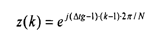
where N may be the FFT size. When sampling the cyclic prefix, a timing offset may be manifested by a growing phase offset when indexed by tone frequency. For a RS tone, a received channel coefficient may be given by the following relationship:
where hrxk may be a received channel coefficient affected by a phase offset z(k), hk may be a channel coefficient without phase offset, and nk may be a noise term. InFIG. 3B , various plots may illustrate a plurality of z(k), for different values of Δtg , where timing offsetplot 350a may correspond to Δtg = 1, timing offsetplot 350b may correspond to Δtg = 2 , timing offsetplot 350c may correspond to Δtg = 3, and timing offsetplot 350d may correspond to Δtg = 4. As illustrated inFIG. 3B , timing offset may introduce linearly decreasing phase as a function of frequency. -
FIG. 3C is a diagram illustrating phase offsets for exemplary timing offsets by subcarrier, in accordance with various embodiments of the invention. Referring toFIG. 3C , there is shown a timing offset plot 352a, which may correspond to Δtg = 0; a timing offset plot 352b, which may correspond to Δtg = 1 forsubcarrier 512; a timing offset plot 352c, which may correspond to Δtg = 2 forsubcarrier 511; and a timing offsetplot 350d, which may correspond to Δtg = 3 for subcarrier 510. - For Δtg > 0, the FFT may be sampled late, and a sampling timing adjustment may be desirable. As illustrated in
FIG. 3C , for late sampling, timing offset may manifest phase offset across the bandwidth of the channel, as illustrated for a plurality of subcarriers by the plots 352a - 352d. In some instances, the slope of the phase offset in function of the frequency may be linear with a positive slope for early sampled FFT, and a negative slope for late sampled FFTs, for example. An exemplary phase detector that may use adjacent RS tones per OFDM symbol may be given by the following relationship:
where a phase change between hrxl and hrx l+6 (another RS tone, spaced 6 subcarriers apart, for example), may be averaged over all desirable tones, and all desirable antennas, which may be Nt terms. -
FIG. 4 is a flow chart illustrating an exemplary timing acquisition and tracking process, in accordance with an embodiment of the invention. After initialization instep 402, the primary and secondary synchronization signals, (PSS) and (SSS), may be decoded instep 404. The decoding of the PSS and SSS may provide coarse timing information for frame and slot synchronization, for example. Using the timing information, theFFT block 320, for example, may generate an FFT of a received signal. From this FFT, theRS extraction block 314, for example, may extract an RS set in theRS extraction block 314. This RS set may be fed to thetiming part 340. Instep 340, thetiming part 340 may track Δtg using the feedback loop depicted inFIG. 3A . Since the output signal to_accum may be generated as a function of Δtg , the to_accum output signal from thethreshold block 310 may carry information about Δtg to thetiming generator 312. Thus, the output signal to_accum may enable tracking of the symbol timing, and adjust the timing of the receiver, for example in thetiming generator 312. Instep 410, thetiming generator 312 may adjust the timing based on the input signal to_accum. The adjusted and tracked timing may be communicatively coupled from thetiming generator 312 to thebuffering block 330, where the timing of the FFT input window may be adjusted correspondingly. - In accordance with an embodiment of the invention, a method and system for a RS timing loop for OFDM symbol synchronization and tracking may comprise tracking symbol timing in an Orthogonal Frequency Division Multiplexing (OFDM) signal based on at least a reference symbol set, as described for
FIG. 2 andFIG. 3A . A receiver timing, as described forFIG. 2 andFIG. 3A , may be adjusted based on at least the symbol timing. - The symbol timing may be tracked by generating an output signal as a function of a guard time Δtg in a phase discrimination feedback loop, for
example timing part 340. The reference symbol (RS) set may be generated in an RS extraction module orcircuit 314, from at least a fast Fourier transform of the received OFDM signal. The receiver timing may be coarsely adjusted and then finely adjusted, for example. The coarse receiver timing adjustment may be based on processing at least a primary synchronization signal and a secondary synchronization signal, as described forFIG. 3A . The reference symbol set may comprise a plurality of time-frequency slots. The plurality of time-frequency slots may change according to a frequency shift and pseudo-noise sequence that modulates the reference symbols. The OFDM signal may conform to a Universal Mobile Telecommunications Standards (UMTS) long-term evolution (LTE) signal. The adjustment of the receiver timing may be controlled via areceiver timing generator 312, for example. - Another embodiment of the invention may provide a machine-readable and/or computer-readable storage and/or medium, having stored thereon, a machine code and/or a computer program having at least one code section executable by a machine and/or a computer, thereby causing the machine and/or computer to perform the steps as described herein for a method and system for a reference signal (RS) timing loop for OFDM symbol synchronization and tracking.
- Accordingly, the present invention may be realized in hardware, software, or a combination of hardware and software. The present invention may be realized in a centralized fashion in at least one computer system, or in a distributed fashion where different elements are spread across several interconnected computer systems. Any kind of computer system or other apparatus adapted for carrying out the methods described herein is suited. A typical combination of hardware and software may be a general-purpose computer system with a computer program that, when being loaded and executed, controls the computer system such that it carries out the methods described herein.
- The present invention may also be embedded in a computer program product, which comprises all the features enabling the implementation of the methods described herein, and which when loaded in a computer system is able to carry out these methods. Computer program in the present context means any expression, in any language, code or notation, of a set of instructions intended to cause a system having an information processing capability to perform a particular function either directly or after either or both of the following: a) conversion to another language, code or notation; b) reproduction in a different material form.
- While the present invention has been described with reference to certain embodiments, it will be understood by those skilled in the art that various changes may be made and equivalents may be substituted without departing from the scope of the present invention. In addition, many modifications may be made to adapt a particular situation or material to the teachings of the present invention without departing from its scope. Therefore, it is intended that the present invention not be limited to the particular embodiment disclosed, but that the present invention will include all embodiments falling within the scope of the appended claims.
Advantageously, the method further comprises generating said output signal in a phase discrimination feedback loop.
Advantageously, the method further comprises generating said reference symbol (RS) set in an RS extraction block, from at least a fast Fourier transform of said received OFDM signal.
Advantageously, the method further comprises finely adjusting said symbol timing.
Advantageously, the method further comprises coarsely adjusting said symbol timing prior to said fine adjustment.
Advantageously, the method further comprises generating said coarse symbol timing adjustment based on processing at least a primary synchronization signal and a secondary synchronization signal.
Advantageously, said reference symbol set comprises a plurality of time-frequency slots.
Advantageously, said plurality of time-frequency slots changes according to a frequency shift and pseudo-noise sequence that modulates said reference symbol set.
Advantageously, said OFDM signal conforms with a Universal Mobile Telecommunications Standards (UMTS) long-term evolution (LTE) signal.
Advantageously, the method further comprises controlling adjustment of said receiver timing via a receiver timing generator.
According to an aspect, a system for processing communication signals comprises:
Advantageously, said one or more circuits generate said output signal in a phase discrimination feedback loop.
Advantageously, said one or more circuits generate said reference symbol (RS) set in an RS extraction block, from at least a fast Fourier transform of said received OFDM signal.
Advantageously, said one or more circuits finely adjust said symbol timing.
Advantageously, said one or more circuits coarsely adjust said symbol timing prior to said fine adjustment.
Advantageously, said one or more circuits generate said coarse symbol timing adjustment based on processing at least a primary synchronization signal and a secondary synchronization signal.
Advantageously, said reference symbol set comprises a plurality of time-frequency slots.
Advantageously, said plurality of time-frequency slots changes according to a time-frequency shift and pseudo-noise sequence that modulates said reference symbol set.
Advantageously, said OFDM signal conforms with a Universal Mobile Telecommunications Standards (UMTS) long-term evolution (LTE) signal.
Advantageously, said one or more circuits control adjustment of said receiver timing via a receiver timing generator.
Claims (10)
- A method for processing communication signals, the method comprising:tracking symbol timing in an Orthogonal Frequency Division Multiplexing (OFDM) signal based on at least a reference symbol set; andadjusting receiver timing based on at least said symbol timing.
- The method according to claim 1, comprising tracking said symbol timing by generating an output signal as a function of a guard time Δtg .
- The method according to claim 2, comprising generating said output signal in a phase discrimination feedback loop.
- The method according to claim 1, comprising generating said reference symbol (RS) set in an RS extraction block, from at least a fast Fourier transform of said received OFDM signal.
- The method according to claim 1, comprising finely adjusting said symbol timing.
- The method according to claim 5, comprising coarsely adjusting said symbol timing prior to said fine adjustment.
- A system for processing communication signals, the system comprising:one or more circuits in a receiver operable to, at least:track symbol timing in an Orthogonal Frequency Division Multiplexing (OFDM) signal, wherein said tracking is based on at least a reference symbol set; andadjust receiver timing based on at least said symbol timing.
- The system according to claim 7, wherein said one or more circuits track said symbol timing by generating an output signal as a function of a guard time Δtg .
- The system according to claim 8, wherein said one or more circuits generate said output signal in a phase discrimination feedback loop.
- The system according to claim 7, wherein said one or more circuits generate said reference symbol (RS) set in an RS extraction block, from at least a fast Fourier transform of said received OFDM signal.
Applications Claiming Priority (1)
| Application Number | Priority Date | Filing Date | Title |
|---|---|---|---|
| US12/184,383 US8174958B2 (en) | 2008-08-01 | 2008-08-01 | Method and system for a reference signal (RS) timing loop for OFDM symbol synchronization and tracking |
Publications (3)
| Publication Number | Publication Date |
|---|---|
| EP2150012A2 true EP2150012A2 (en) | 2010-02-03 |
| EP2150012A3 EP2150012A3 (en) | 2012-05-23 |
| EP2150012B1 EP2150012B1 (en) | 2015-11-04 |
Family
ID=41263700
Family Applications (1)
| Application Number | Title | Priority Date | Filing Date |
|---|---|---|---|
| EP09009389.9A Active EP2150012B1 (en) | 2008-08-01 | 2009-07-20 | Method and system for rs timing loop for ofdm symbol synchronization and tracking |
Country Status (5)
| Country | Link |
|---|---|
| US (3) | US8174958B2 (en) |
| EP (1) | EP2150012B1 (en) |
| KR (1) | KR101165266B1 (en) |
| CN (1) | CN101640659B (en) |
| TW (1) | TWI416915B (en) |
Families Citing this family (10)
| Publication number | Priority date | Publication date | Assignee | Title |
|---|---|---|---|---|
| US8174958B2 (en) | 2008-08-01 | 2012-05-08 | Broadcom Corporation | Method and system for a reference signal (RS) timing loop for OFDM symbol synchronization and tracking |
| US9094906B2 (en) * | 2011-11-11 | 2015-07-28 | Telefonaktiebolaget Lm Ericsson (Publ) | Multi-stage timing and frequency synchronization |
| KR101903375B1 (en) | 2012-12-13 | 2018-11-07 | 삼성전자주식회사 | Communicatin system including multiple receiving antennas and time tracking method thereof |
| US20150318982A1 (en) | 2014-05-05 | 2015-11-05 | Andrew M. Kowalevicz | Method and system for non-persistent communication |
| KR102332471B1 (en) | 2015-05-08 | 2021-11-30 | 삼성전자주식회사 | Apparatus and method for synchronization signal detecting |
| WO2018061599A1 (en) * | 2016-09-29 | 2018-04-05 | シャープ株式会社 | Terminal device, base station device, communication method, and integrated circuit |
| KR102420816B1 (en) | 2018-04-05 | 2022-07-14 | 삼성전자 주식회사 | Method and apparatus for decoding data in a wireless communication system |
| EP3748512B1 (en) * | 2019-06-06 | 2023-08-02 | Infineon Technologies AG | Method for a slave device for calibrating its output timing, method for a master device for enabling a slave device to calibrate its output timing, master device and slave device |
| WO2022238540A1 (en) | 2021-05-12 | 2022-11-17 | Telefonaktiebolaget Lm Ericsson (Publ) | Methods and devices for network link measurement |
| EP4364477A4 (en) * | 2021-06-30 | 2024-07-31 | Telefonaktiebolaget LM Ericsson (publ) | PURPOSE-DEPENDENT DETERMINATION OF A RECEIVER SYMBOL PROCESSING WINDOW |
Family Cites Families (38)
| Publication number | Priority date | Publication date | Assignee | Title |
|---|---|---|---|---|
| US20010055320A1 (en) * | 1994-12-15 | 2001-12-27 | Pierzga Wayne Francis | Multiplex communication |
| AU740804B2 (en) * | 1999-07-19 | 2001-11-15 | Nippon Telegraph & Telephone Corporation | OFDM packet communication receiver system |
| KR100793217B1 (en) * | 1999-10-22 | 2008-01-10 | 넥스트넷 와이어리스 인크. | System and method for delivering data packets as framed downlink and unframed uplink |
| AU2001271322A1 (en) * | 2000-06-16 | 2002-01-02 | Inari, Inc. | Sliding-window processing for the reception of multicarrier signals |
| KR100666691B1 (en) * | 2000-12-06 | 2007-01-11 | 삼성전자주식회사 | Receiving device of OFM signal and signal restoration method through channel estimation |
| US7012881B2 (en) * | 2000-12-29 | 2006-03-14 | Samsung Electronic Co., Ltd. | Timing and frequency offset estimation scheme for OFDM systems by using an analytic tone |
| US7158474B1 (en) * | 2001-02-21 | 2007-01-02 | At&T Corp. | Interference suppressing OFDM system for wireless communications |
| US7248652B2 (en) * | 2001-02-28 | 2007-07-24 | Agere Systems Inc. | Method and apparatus for recovering timing information in orthogonal frequency division multiplexing (OFDM) systems |
| US7218691B1 (en) * | 2001-03-05 | 2007-05-15 | Marvell International Ltd. | Method and apparatus for estimation of orthogonal frequency division multiplexing symbol timing and carrier frequency offset |
| US7020218B2 (en) * | 2001-06-18 | 2006-03-28 | Arnesen David M | Sliding-window transform with integrated windowing |
| GB2376855A (en) * | 2001-06-20 | 2002-12-24 | Sony Uk Ltd | Determining symbol synchronisation in an OFDM receiver in response to one of two impulse response estimates |
| US7103116B2 (en) * | 2001-09-24 | 2006-09-05 | Atheros Communications, Inc. | Detection of a false detection of a communication packet |
| GB2395094A (en) * | 2002-10-28 | 2004-05-12 | Sony Uk Ltd | Determining a symbol synch time in an OFDM receiver |
| JP2004214962A (en) * | 2002-12-27 | 2004-07-29 | Sony Corp | Ofdm demodulator |
| JP2004214963A (en) * | 2002-12-27 | 2004-07-29 | Sony Corp | OFDM demodulator |
| CN1297089C (en) * | 2003-03-14 | 2007-01-24 | 北京泰美世纪科技有限公司 | Continuous pilot frequency data transmission method based on OFDM frequency hop in broadcasting system |
| CN100576834C (en) * | 2003-03-28 | 2009-12-30 | 英特尔公司 | Method and apparatus for OFDM symbol timing synchronization |
| CN1306745C (en) * | 2003-05-30 | 2007-03-21 | 电子科技大学 | Guiding plan based on time frequency synchronous training sequence |
| US7251283B2 (en) * | 2003-10-20 | 2007-07-31 | Mediatek, Inc. | Timing offset compensation in orthogonal frequency division multiplexing systems |
| GB2412551A (en) * | 2004-03-26 | 2005-09-28 | Sony Uk Ltd | Receiver |
| KR100688118B1 (en) * | 2004-04-23 | 2007-02-28 | 삼성전자주식회사 | Apparatus and Method for Reducing Peak to Average Power Ratio in Orthogonal Frequency Division Multiple Communication Systems |
| US7457231B2 (en) * | 2004-05-04 | 2008-11-25 | Qualcomm Incorporated | Staggered pilot transmission for channel estimation and time tracking |
| WO2005125136A1 (en) * | 2004-06-08 | 2005-12-29 | Sandbridge Technologies, Inc. | Orthogonal frequency division multiplexing receiver |
| US20050286485A1 (en) * | 2004-06-23 | 2005-12-29 | Golden Stuart A | Fast and robust timing acquisition algorithm |
| US8144824B2 (en) * | 2005-03-10 | 2012-03-27 | Qualcomm Incorporated | Trend influenced time tracking |
| US20060221810A1 (en) * | 2005-03-10 | 2006-10-05 | Bojan Vrcelj | Fine timing acquisition |
| US7539125B2 (en) * | 2005-10-14 | 2009-05-26 | Via Technologies, Inc. | Method and circuit for frequency offset estimation in frequency domain in the orthogonal frequency division multiplexing baseband receiver for IEEE 802.11A/G wireless LAN standard |
| US7532676B2 (en) * | 2005-10-20 | 2009-05-12 | Trellis Phase Communications, Lp | Single sideband and quadrature multiplexed continuous phase modulation |
| JP2009519664A (en) * | 2005-12-16 | 2009-05-14 | エヌエックスピー ビー ヴィ | Method and system for estimating symbol time error in a broadband transmission system |
| JP2007258819A (en) * | 2006-03-20 | 2007-10-04 | Casio Comput Co Ltd | OFDM receiving apparatus, OFDM receiving method, and terrestrial digital receiving apparatus |
| EP2055062A1 (en) * | 2006-08-18 | 2009-05-06 | Nxp B.V. | Time error estimation for data symbols |
| JP4769162B2 (en) * | 2006-10-13 | 2011-09-07 | ニスカ株式会社 | Sheet stacking apparatus and image forming apparatus provided with the same |
| US8942150B2 (en) * | 2007-03-19 | 2015-01-27 | Qualcomm Incorporated | Uplink timing control |
| US8169992B2 (en) * | 2007-08-08 | 2012-05-01 | Telefonaktiebolaget Lm Ericsson (Publ) | Uplink scrambling during random access |
| US20090059782A1 (en) * | 2007-08-29 | 2009-03-05 | Rgb Systems, Inc. | Method and apparatus for extending the transmission capability of twisted pair communication systems |
| US8774103B2 (en) * | 2008-03-26 | 2014-07-08 | Broadcom Corporation | Selecting uplink sounding sub-carriers |
| US8174958B2 (en) * | 2008-08-01 | 2012-05-08 | Broadcom Corporation | Method and system for a reference signal (RS) timing loop for OFDM symbol synchronization and tracking |
| US8559296B2 (en) * | 2008-08-01 | 2013-10-15 | Broadcom Corporation | Method and system for an OFDM joint timing and frequency tracking system |
-
2008
- 2008-08-01 US US12/184,383 patent/US8174958B2/en active Active
-
2009
- 2009-07-20 EP EP09009389.9A patent/EP2150012B1/en active Active
- 2009-07-31 KR KR1020090070882A patent/KR101165266B1/en not_active Expired - Fee Related
- 2009-07-31 TW TW098125935A patent/TWI416915B/en active
- 2009-08-03 CN CN2009101641721A patent/CN101640659B/en active Active
-
2012
- 2012-05-07 US US13/465,451 patent/US8498197B2/en not_active Expired - Fee Related
-
2013
- 2013-06-18 US US13/920,947 patent/US8824269B2/en not_active Expired - Fee Related
Non-Patent Citations (1)
| Title |
|---|
| None |
Also Published As
| Publication number | Publication date |
|---|---|
| US8174958B2 (en) | 2012-05-08 |
| US20120275552A1 (en) | 2012-11-01 |
| TW201021483A (en) | 2010-06-01 |
| EP2150012A3 (en) | 2012-05-23 |
| HK1138691A1 (en) | 2010-08-27 |
| US8498197B2 (en) | 2013-07-30 |
| CN101640659A (en) | 2010-02-03 |
| EP2150012B1 (en) | 2015-11-04 |
| TWI416915B (en) | 2013-11-21 |
| US20100027499A1 (en) | 2010-02-04 |
| KR101165266B1 (en) | 2012-07-19 |
| US20130279637A1 (en) | 2013-10-24 |
| CN101640659B (en) | 2012-12-12 |
| KR20100014196A (en) | 2010-02-10 |
| US8824269B2 (en) | 2014-09-02 |
Similar Documents
| Publication | Publication Date | Title |
|---|---|---|
| US8929197B2 (en) | Method and system for an OFDM joint training and frequency tracking system | |
| US8824269B2 (en) | Method and system for a reference signal (RS) timing loop for OFDM symbol synchronization and tracking | |
| US8170592B2 (en) | Method and system for frame timing acquisition in evolved universal terrestrial radio access (EUTRA) | |
| US6993084B1 (en) | Coarse frequency synchronisation in multicarrier systems | |
| US7254196B2 (en) | Symbol timing for MIMO OFDM and other wireless communication systems | |
| US6850481B2 (en) | Channels estimation for multiple input—multiple output, orthogonal frequency division multiplexing (OFDM) system | |
| US8380151B2 (en) | Method and system for reducing the complexity of multi-frequency hypothesis testing using an iterative approach | |
| MR et al. | A complete cell search and synchronization in LTE | |
| US8223891B2 (en) | Method and system for a reference symbol (RS) frequency control loop for TCXO synchronization and tracking | |
| CN114786240B (en) | 5G downlink signal intermittent tracking method | |
| US20100046359A1 (en) | Wireless Terminal, Base Station and Channel Characteristic Estimating Method | |
| Yoon et al. | Recovery of carrier frequency offset and set information for LTE device-to-device communications | |
| Wang et al. | A low-complexity joint time synchronization and channel estimation scheme for orthogonal frequency division multiplexing systems | |
| Magani et al. | Cell-search and tracking of residual time and frequency offsets in low power NB-IoT devices | |
| HK1138691B (en) | Method and system for processing communication signals | |
| Roman et al. | Carrier frequency synchronization for mobile television receivers | |
| KR20190066992A (en) | Terminal and operating method therefof in internet of things | |
| Langowski | Carrier and sampling frequency offset estimation and tracking in OFDM systems | |
| HK1138693B (en) | Method and system for an ofdm joint timing and frequency tracking system | |
| Fedra et al. | Low computing complexity frame synchronization for OFDM communication |
Legal Events
| Date | Code | Title | Description |
|---|---|---|---|
| PUAI | Public reference made under article 153(3) epc to a published international application that has entered the european phase |
Free format text: ORIGINAL CODE: 0009012 |
|
| AK | Designated contracting states |
Kind code of ref document: A2 Designated state(s): AT BE BG CH CY CZ DE DK EE ES FI FR GB GR HR HU IE IS IT LI LT LU LV MC MK MT NL NO PL PT RO SE SI SK SM TR |
|
| AX | Request for extension of the european patent |
Extension state: AL BA RS |
|
| PUAL | Search report despatched |
Free format text: ORIGINAL CODE: 0009013 |
|
| AK | Designated contracting states |
Kind code of ref document: A3 Designated state(s): AT BE BG CH CY CZ DE DK EE ES FI FR GB GR HR HU IE IS IT LI LT LU LV MC MK MT NL NO PL PT RO SE SI SK SM TR |
|
| AX | Request for extension of the european patent |
Extension state: AL BA RS |
|
| RIC1 | Information provided on ipc code assigned before grant |
Ipc: H04L 27/26 20060101AFI20120418BHEP |
|
| 17P | Request for examination filed |
Effective date: 20121123 |
|
| 17Q | First examination report despatched |
Effective date: 20130211 |
|
| GRAP | Despatch of communication of intention to grant a patent |
Free format text: ORIGINAL CODE: EPIDOSNIGR1 |
|
| INTG | Intention to grant announced |
Effective date: 20150603 |
|
| RIC1 | Information provided on ipc code assigned before grant |
Ipc: H04L 27/26 20060101AFI20150526BHEP Ipc: H04L 7/00 20060101ALI20150526BHEP |
|
| GRAS | Grant fee paid |
Free format text: ORIGINAL CODE: EPIDOSNIGR3 |
|
| GRAA | (expected) grant |
Free format text: ORIGINAL CODE: 0009210 |
|
| AK | Designated contracting states |
Kind code of ref document: B1 Designated state(s): AT BE BG CH CY CZ DE DK EE ES FI FR GB GR HR HU IE IS IT LI LT LU LV MC MK MT NL NO PL PT RO SE SI SK SM TR |
|
| REG | Reference to a national code |
Ref country code: GB Ref legal event code: FG4D |
|
| REG | Reference to a national code |
Ref country code: CH Ref legal event code: EP |
|
| REG | Reference to a national code |
Ref country code: AT Ref legal event code: REF Ref document number: 759849 Country of ref document: AT Kind code of ref document: T Effective date: 20151115 |
|
| REG | Reference to a national code |
Ref country code: IE Ref legal event code: FG4D |
|
| REG | Reference to a national code |
Ref country code: DE Ref legal event code: R096 Ref document number: 602009034572 Country of ref document: DE |
|
| REG | Reference to a national code |
Ref country code: NL Ref legal event code: MP Effective date: 20151104 |
|
| REG | Reference to a national code |
Ref country code: LT Ref legal event code: MG4D |
|
| REG | Reference to a national code |
Ref country code: AT Ref legal event code: MK05 Ref document number: 759849 Country of ref document: AT Kind code of ref document: T Effective date: 20151104 |
|
| PG25 | Lapsed in a contracting state [announced via postgrant information from national office to epo] |
Ref country code: ES Free format text: LAPSE BECAUSE OF FAILURE TO SUBMIT A TRANSLATION OF THE DESCRIPTION OR TO PAY THE FEE WITHIN THE PRESCRIBED TIME-LIMIT Effective date: 20151104 Ref country code: IS Free format text: LAPSE BECAUSE OF FAILURE TO SUBMIT A TRANSLATION OF THE DESCRIPTION OR TO PAY THE FEE WITHIN THE PRESCRIBED TIME-LIMIT Effective date: 20160304 Ref country code: IT Free format text: LAPSE BECAUSE OF FAILURE TO SUBMIT A TRANSLATION OF THE DESCRIPTION OR TO PAY THE FEE WITHIN THE PRESCRIBED TIME-LIMIT Effective date: 20151104 Ref country code: NL Free format text: LAPSE BECAUSE OF FAILURE TO SUBMIT A TRANSLATION OF THE DESCRIPTION OR TO PAY THE FEE WITHIN THE PRESCRIBED TIME-LIMIT Effective date: 20151104 Ref country code: LT Free format text: LAPSE BECAUSE OF FAILURE TO SUBMIT A TRANSLATION OF THE DESCRIPTION OR TO PAY THE FEE WITHIN THE PRESCRIBED TIME-LIMIT Effective date: 20151104 Ref country code: NO Free format text: LAPSE BECAUSE OF FAILURE TO SUBMIT A TRANSLATION OF THE DESCRIPTION OR TO PAY THE FEE WITHIN THE PRESCRIBED TIME-LIMIT Effective date: 20160204 Ref country code: HR Free format text: LAPSE BECAUSE OF FAILURE TO SUBMIT A TRANSLATION OF THE DESCRIPTION OR TO PAY THE FEE WITHIN THE PRESCRIBED TIME-LIMIT Effective date: 20151104 |
|
| PG25 | Lapsed in a contracting state [announced via postgrant information from national office to epo] |
Ref country code: FI Free format text: LAPSE BECAUSE OF FAILURE TO SUBMIT A TRANSLATION OF THE DESCRIPTION OR TO PAY THE FEE WITHIN THE PRESCRIBED TIME-LIMIT Effective date: 20151104 Ref country code: PL Free format text: LAPSE BECAUSE OF FAILURE TO SUBMIT A TRANSLATION OF THE DESCRIPTION OR TO PAY THE FEE WITHIN THE PRESCRIBED TIME-LIMIT Effective date: 20151104 Ref country code: PT Free format text: LAPSE BECAUSE OF FAILURE TO SUBMIT A TRANSLATION OF THE DESCRIPTION OR TO PAY THE FEE WITHIN THE PRESCRIBED TIME-LIMIT Effective date: 20160304 Ref country code: GR Free format text: LAPSE BECAUSE OF FAILURE TO SUBMIT A TRANSLATION OF THE DESCRIPTION OR TO PAY THE FEE WITHIN THE PRESCRIBED TIME-LIMIT Effective date: 20160205 Ref country code: SE Free format text: LAPSE BECAUSE OF FAILURE TO SUBMIT A TRANSLATION OF THE DESCRIPTION OR TO PAY THE FEE WITHIN THE PRESCRIBED TIME-LIMIT Effective date: 20151104 Ref country code: LV Free format text: LAPSE BECAUSE OF FAILURE TO SUBMIT A TRANSLATION OF THE DESCRIPTION OR TO PAY THE FEE WITHIN THE PRESCRIBED TIME-LIMIT Effective date: 20151104 Ref country code: AT Free format text: LAPSE BECAUSE OF FAILURE TO SUBMIT A TRANSLATION OF THE DESCRIPTION OR TO PAY THE FEE WITHIN THE PRESCRIBED TIME-LIMIT Effective date: 20151104 |
|
| PG25 | Lapsed in a contracting state [announced via postgrant information from national office to epo] |
Ref country code: CZ Free format text: LAPSE BECAUSE OF FAILURE TO SUBMIT A TRANSLATION OF THE DESCRIPTION OR TO PAY THE FEE WITHIN THE PRESCRIBED TIME-LIMIT Effective date: 20151104 |
|
| REG | Reference to a national code |
Ref country code: DE Ref legal event code: R097 Ref document number: 602009034572 Country of ref document: DE |
|
| PG25 | Lapsed in a contracting state [announced via postgrant information from national office to epo] |
Ref country code: EE Free format text: LAPSE BECAUSE OF FAILURE TO SUBMIT A TRANSLATION OF THE DESCRIPTION OR TO PAY THE FEE WITHIN THE PRESCRIBED TIME-LIMIT Effective date: 20151104 Ref country code: DK Free format text: LAPSE BECAUSE OF FAILURE TO SUBMIT A TRANSLATION OF THE DESCRIPTION OR TO PAY THE FEE WITHIN THE PRESCRIBED TIME-LIMIT Effective date: 20151104 Ref country code: SM Free format text: LAPSE BECAUSE OF FAILURE TO SUBMIT A TRANSLATION OF THE DESCRIPTION OR TO PAY THE FEE WITHIN THE PRESCRIBED TIME-LIMIT Effective date: 20151104 Ref country code: RO Free format text: LAPSE BECAUSE OF FAILURE TO SUBMIT A TRANSLATION OF THE DESCRIPTION OR TO PAY THE FEE WITHIN THE PRESCRIBED TIME-LIMIT Effective date: 20151104 Ref country code: SK Free format text: LAPSE BECAUSE OF FAILURE TO SUBMIT A TRANSLATION OF THE DESCRIPTION OR TO PAY THE FEE WITHIN THE PRESCRIBED TIME-LIMIT Effective date: 20151104 |
|
| PLBE | No opposition filed within time limit |
Free format text: ORIGINAL CODE: 0009261 |
|
| STAA | Information on the status of an ep patent application or granted ep patent |
Free format text: STATUS: NO OPPOSITION FILED WITHIN TIME LIMIT |
|
| 26N | No opposition filed |
Effective date: 20160805 |
|
| PG25 | Lapsed in a contracting state [announced via postgrant information from national office to epo] |
Ref country code: SI Free format text: LAPSE BECAUSE OF FAILURE TO SUBMIT A TRANSLATION OF THE DESCRIPTION OR TO PAY THE FEE WITHIN THE PRESCRIBED TIME-LIMIT Effective date: 20151104 |
|
| PG25 | Lapsed in a contracting state [announced via postgrant information from national office to epo] |
Ref country code: BE Free format text: LAPSE BECAUSE OF FAILURE TO SUBMIT A TRANSLATION OF THE DESCRIPTION OR TO PAY THE FEE WITHIN THE PRESCRIBED TIME-LIMIT Effective date: 20151104 |
|
| REG | Reference to a national code |
Ref country code: FR Ref legal event code: PLFP Year of fee payment: 8 |
|
| REG | Reference to a national code |
Ref country code: CH Ref legal event code: PL |
|
| REG | Reference to a national code |
Ref country code: DE Ref legal event code: R082 Ref document number: 602009034572 Country of ref document: DE Representative=s name: BOSCH JEHLE PATENTANWALTSGESELLSCHAFT MBH, DE Ref country code: DE Ref legal event code: R081 Ref document number: 602009034572 Country of ref document: DE Owner name: AVAGO TECHNOLOGIES INTERNATIONAL SALES PTE. LT, SG Free format text: FORMER OWNER: BROADCOM CORP., IRVINE, CALIF., US Ref country code: DE Ref legal event code: R081 Ref document number: 602009034572 Country of ref document: DE Owner name: AVAGO TECHNOLOGIES GENERAL IP (SINGAPORE) PTE., SG Free format text: FORMER OWNER: BROADCOM CORP., IRVINE, CALIF., US |
|
| GBPC | Gb: european patent ceased through non-payment of renewal fee |
Effective date: 20160720 |
|
| PG25 | Lapsed in a contracting state [announced via postgrant information from national office to epo] |
Ref country code: MC Free format text: LAPSE BECAUSE OF FAILURE TO SUBMIT A TRANSLATION OF THE DESCRIPTION OR TO PAY THE FEE WITHIN THE PRESCRIBED TIME-LIMIT Effective date: 20151104 |
|
| PG25 | Lapsed in a contracting state [announced via postgrant information from national office to epo] |
Ref country code: CH Free format text: LAPSE BECAUSE OF NON-PAYMENT OF DUE FEES Effective date: 20160731 Ref country code: LI Free format text: LAPSE BECAUSE OF NON-PAYMENT OF DUE FEES Effective date: 20160731 |
|
| REG | Reference to a national code |
Ref country code: IE Ref legal event code: MM4A |
|
| PG25 | Lapsed in a contracting state [announced via postgrant information from national office to epo] |
Ref country code: GB Free format text: LAPSE BECAUSE OF NON-PAYMENT OF DUE FEES Effective date: 20160720 |
|
| REG | Reference to a national code |
Ref country code: FR Ref legal event code: PLFP Year of fee payment: 9 |
|
| PG25 | Lapsed in a contracting state [announced via postgrant information from national office to epo] |
Ref country code: IE Free format text: LAPSE BECAUSE OF NON-PAYMENT OF DUE FEES Effective date: 20160720 |
|
| PG25 | Lapsed in a contracting state [announced via postgrant information from national office to epo] |
Ref country code: LU Free format text: LAPSE BECAUSE OF NON-PAYMENT OF DUE FEES Effective date: 20160720 |
|
| PGFP | Annual fee paid to national office [announced via postgrant information from national office to epo] |
Ref country code: NO Payment date: 20170725 Year of fee payment: 9 |
|
| REG | Reference to a national code |
Ref country code: GB Ref legal event code: 732E Free format text: REGISTERED BETWEEN 20171005 AND 20171011 |
|
| REG | Reference to a national code |
Ref country code: FR Ref legal event code: TP Owner name: AVAGO TECHNOLOGIES GENERAL IP PTE. LTD., SG Effective date: 20180228 |
|
| PG25 | Lapsed in a contracting state [announced via postgrant information from national office to epo] |
Ref country code: CY Free format text: LAPSE BECAUSE OF FAILURE TO SUBMIT A TRANSLATION OF THE DESCRIPTION OR TO PAY THE FEE WITHIN THE PRESCRIBED TIME-LIMIT Effective date: 20151104 Ref country code: HU Free format text: LAPSE BECAUSE OF FAILURE TO SUBMIT A TRANSLATION OF THE DESCRIPTION OR TO PAY THE FEE WITHIN THE PRESCRIBED TIME-LIMIT; INVALID AB INITIO Effective date: 20090720 |
|
| PG25 | Lapsed in a contracting state [announced via postgrant information from national office to epo] |
Ref country code: MK Free format text: LAPSE BECAUSE OF FAILURE TO SUBMIT A TRANSLATION OF THE DESCRIPTION OR TO PAY THE FEE WITHIN THE PRESCRIBED TIME-LIMIT Effective date: 20151104 Ref country code: TR Free format text: LAPSE BECAUSE OF FAILURE TO SUBMIT A TRANSLATION OF THE DESCRIPTION OR TO PAY THE FEE WITHIN THE PRESCRIBED TIME-LIMIT Effective date: 20151104 Ref country code: MT Free format text: LAPSE BECAUSE OF NON-PAYMENT OF DUE FEES Effective date: 20160731 |
|
| PG25 | Lapsed in a contracting state [announced via postgrant information from national office to epo] |
Ref country code: BG Free format text: LAPSE BECAUSE OF FAILURE TO SUBMIT A TRANSLATION OF THE DESCRIPTION OR TO PAY THE FEE WITHIN THE PRESCRIBED TIME-LIMIT Effective date: 20151104 |
|
| REG | Reference to a national code |
Ref country code: DE Ref legal event code: R082 Ref document number: 602009034572 Country of ref document: DE Representative=s name: BOSCH JEHLE PATENTANWALTSGESELLSCHAFT MBH, DE Ref country code: DE Ref legal event code: R081 Ref document number: 602009034572 Country of ref document: DE Owner name: AVAGO TECHNOLOGIES INTERNATIONAL SALES PTE. LT, SG Free format text: FORMER OWNER: AVAGO TECHNOLOGIES GENERAL IP (SINGAPORE) PTE. LTD., SINGAPORE, SG |
|
| REG | Reference to a national code |
Ref country code: GB Ref legal event code: 732E Free format text: REGISTERED BETWEEN 20190222 AND 20190227 |
|
| PG25 | Lapsed in a contracting state [announced via postgrant information from national office to epo] |
Ref country code: FR Free format text: LAPSE BECAUSE OF NON-PAYMENT OF DUE FEES Effective date: 20180731 |
|
| PGFP | Annual fee paid to national office [announced via postgrant information from national office to epo] |
Ref country code: DE Payment date: 20250710 Year of fee payment: 17 |