EP2148378B1 - Couches barrière dans des cellules solaires métamorphiques multijonctions inversées - Google Patents
Couches barrière dans des cellules solaires métamorphiques multijonctions inversées Download PDFInfo
- Publication number
- EP2148378B1 EP2148378B1 EP08013467A EP08013467A EP2148378B1 EP 2148378 B1 EP2148378 B1 EP 2148378B1 EP 08013467 A EP08013467 A EP 08013467A EP 08013467 A EP08013467 A EP 08013467A EP 2148378 B1 EP2148378 B1 EP 2148378B1
- Authority
- EP
- European Patent Office
- Prior art keywords
- subcell
- solar cell
- band gap
- solar
- barrier layer
- Prior art date
- Legal status (The legal status is an assumption and is not a legal conclusion. Google has not performed a legal analysis and makes no representation as to the accuracy of the status listed.)
- Revoked
Links
- 230000004888 barrier function Effects 0.000 title claims abstract description 40
- 239000010410 layer Substances 0.000 claims abstract description 119
- 238000000034 method Methods 0.000 claims abstract description 42
- 239000000758 substrate Substances 0.000 claims abstract description 28
- 239000011229 interlayer Substances 0.000 claims abstract description 18
- 239000004065 semiconductor Substances 0.000 claims abstract description 17
- 239000000463 material Substances 0.000 claims abstract description 13
- 239000000203 mixture Substances 0.000 claims description 7
- 229910052785 arsenic Inorganic materials 0.000 claims description 6
- 150000001875 compounds Chemical class 0.000 claims description 6
- 229910052757 nitrogen Inorganic materials 0.000 claims description 6
- 229910000530 Gallium indium arsenide Inorganic materials 0.000 claims description 5
- 240000002329 Inga feuillei Species 0.000 claims description 5
- 229910052698 phosphorus Inorganic materials 0.000 claims description 5
- 229910052787 antimony Inorganic materials 0.000 claims description 4
- 229910052732 germanium Inorganic materials 0.000 claims description 4
- GNPVGFCGXDBREM-UHFFFAOYSA-N germanium atom Chemical compound [Ge] GNPVGFCGXDBREM-UHFFFAOYSA-N 0.000 claims description 4
- 230000001902 propagating effect Effects 0.000 claims description 4
- 238000005530 etching Methods 0.000 claims description 3
- 229910001218 Gallium arsenide Inorganic materials 0.000 claims 3
- 238000000151 deposition Methods 0.000 claims 1
- 238000000059 patterning Methods 0.000 claims 1
- 210000004027 cell Anatomy 0.000 description 78
- 229910052751 metal Inorganic materials 0.000 description 6
- 239000002184 metal Substances 0.000 description 6
- 230000006798 recombination Effects 0.000 description 6
- 238000005215 recombination Methods 0.000 description 6
- 238000005259 measurement Methods 0.000 description 5
- CIWBSHSKHKDKBQ-JLAZNSOCSA-N Ascorbic acid Chemical compound OC[C@H](O)[C@H]1OC(=O)C(O)=C1O CIWBSHSKHKDKBQ-JLAZNSOCSA-N 0.000 description 4
- 239000000853 adhesive Substances 0.000 description 4
- 230000001070 adhesive effect Effects 0.000 description 4
- 230000003667 anti-reflective effect Effects 0.000 description 3
- 238000006243 chemical reaction Methods 0.000 description 3
- KRKNYBCHXYNGOX-UHFFFAOYSA-N citric acid Chemical compound OC(=O)CC(O)(C(O)=O)CC(O)=O KRKNYBCHXYNGOX-UHFFFAOYSA-N 0.000 description 3
- 239000000126 substance Substances 0.000 description 3
- IJGRMHOSHXDMSA-UHFFFAOYSA-N Atomic nitrogen Chemical compound N#N IJGRMHOSHXDMSA-UHFFFAOYSA-N 0.000 description 2
- 238000010276 construction Methods 0.000 description 2
- 230000001419 dependent effect Effects 0.000 description 2
- 239000002019 doping agent Substances 0.000 description 2
- 238000004519 manufacturing process Methods 0.000 description 2
- 230000006911 nucleation Effects 0.000 description 2
- 238000010899 nucleation Methods 0.000 description 2
- 241000894007 species Species 0.000 description 2
- RDEIXVOBVLKYNT-VQBXQJRRSA-N (2r,3r,4r,5r)-2-[(1s,2s,3r,4s,6r)-4,6-diamino-3-[(2r,3r,6s)-3-amino-6-(1-aminoethyl)oxan-2-yl]oxy-2-hydroxycyclohexyl]oxy-5-methyl-4-(methylamino)oxane-3,5-diol;(2r,3r,4r,5r)-2-[(1s,2s,3r,4s,6r)-4,6-diamino-3-[(2r,3r,6s)-3-amino-6-(aminomethyl)oxan-2-yl]o Chemical compound OS(O)(=O)=O.O1C[C@@](O)(C)[C@H](NC)[C@@H](O)[C@H]1O[C@@H]1[C@@H](O)[C@H](O[C@@H]2[C@@H](CC[C@@H](CN)O2)N)[C@@H](N)C[C@H]1N.O1C[C@@](O)(C)[C@H](NC)[C@@H](O)[C@H]1O[C@@H]1[C@@H](O)[C@H](O[C@@H]2[C@@H](CC[C@H](O2)C(C)N)N)[C@@H](N)C[C@H]1N.O1[C@H](C(C)NC)CC[C@@H](N)[C@H]1O[C@H]1[C@H](O)[C@@H](O[C@@H]2[C@@H]([C@@H](NC)[C@@](C)(O)CO2)O)[C@H](N)C[C@@H]1N RDEIXVOBVLKYNT-VQBXQJRRSA-N 0.000 description 1
- 229910000980 Aluminium gallium arsenide Inorganic materials 0.000 description 1
- JBRZTFJDHDCESZ-UHFFFAOYSA-N AsGa Chemical compound [As]#[Ga] JBRZTFJDHDCESZ-UHFFFAOYSA-N 0.000 description 1
- ZOXJGFHDIHLPTG-UHFFFAOYSA-N Boron Chemical compound [B] ZOXJGFHDIHLPTG-UHFFFAOYSA-N 0.000 description 1
- OKTJSMMVPCPJKN-UHFFFAOYSA-N Carbon Chemical compound [C] OKTJSMMVPCPJKN-UHFFFAOYSA-N 0.000 description 1
- -1 GaInPAs Inorganic materials 0.000 description 1
- GYHNNYVSQQEPJS-UHFFFAOYSA-N Gallium Chemical compound [Ga] GYHNNYVSQQEPJS-UHFFFAOYSA-N 0.000 description 1
- XUIMIQQOPSSXEZ-UHFFFAOYSA-N Silicon Chemical compound [Si] XUIMIQQOPSSXEZ-UHFFFAOYSA-N 0.000 description 1
- BQCADISMDOOEFD-UHFFFAOYSA-N Silver Chemical compound [Ag] BQCADISMDOOEFD-UHFFFAOYSA-N 0.000 description 1
- ATJFFYVFTNAWJD-UHFFFAOYSA-N Tin Chemical compound [Sn] ATJFFYVFTNAWJD-UHFFFAOYSA-N 0.000 description 1
- 230000006978 adaptation Effects 0.000 description 1
- 239000012790 adhesive layer Substances 0.000 description 1
- 229910052782 aluminium Inorganic materials 0.000 description 1
- XAGFODPZIPBFFR-UHFFFAOYSA-N aluminium Chemical compound [Al] XAGFODPZIPBFFR-UHFFFAOYSA-N 0.000 description 1
- 238000004458 analytical method Methods 0.000 description 1
- WATWJIUSRGPENY-UHFFFAOYSA-N antimony atom Chemical compound [Sb] WATWJIUSRGPENY-UHFFFAOYSA-N 0.000 description 1
- 238000013459 approach Methods 0.000 description 1
- 238000003491 array Methods 0.000 description 1
- RQNWIZPPADIBDY-UHFFFAOYSA-N arsenic atom Chemical compound [As] RQNWIZPPADIBDY-UHFFFAOYSA-N 0.000 description 1
- 230000015572 biosynthetic process Effects 0.000 description 1
- 229910052797 bismuth Inorganic materials 0.000 description 1
- JCXGWMGPZLAOME-UHFFFAOYSA-N bismuth atom Chemical compound [Bi] JCXGWMGPZLAOME-UHFFFAOYSA-N 0.000 description 1
- 229910052796 boron Inorganic materials 0.000 description 1
- 229910052799 carbon Inorganic materials 0.000 description 1
- 239000000969 carrier Substances 0.000 description 1
- 230000015556 catabolic process Effects 0.000 description 1
- 238000005136 cathodoluminescence Methods 0.000 description 1
- 230000011712 cell development Effects 0.000 description 1
- 239000011247 coating layer Substances 0.000 description 1
- 238000004891 communication Methods 0.000 description 1
- 239000000470 constituent Substances 0.000 description 1
- 239000006059 cover glass Substances 0.000 description 1
- 238000006731 degradation reaction Methods 0.000 description 1
- 238000011161 development Methods 0.000 description 1
- 230000018109 developmental process Effects 0.000 description 1
- 238000001152 differential interference contrast microscopy Methods 0.000 description 1
- 230000000694 effects Effects 0.000 description 1
- 230000008020 evaporation Effects 0.000 description 1
- 238000001704 evaporation Methods 0.000 description 1
- 229910052733 gallium Inorganic materials 0.000 description 1
- 229940084896 gentak Drugs 0.000 description 1
- BHEPBYXIRTUNPN-UHFFFAOYSA-N hydridophosphorus(.) (triplet) Chemical compound [PH] BHEPBYXIRTUNPN-UHFFFAOYSA-N 0.000 description 1
- 229910052738 indium Inorganic materials 0.000 description 1
- APFVFJFRJDLVQX-UHFFFAOYSA-N indium atom Chemical compound [In] APFVFJFRJDLVQX-UHFFFAOYSA-N 0.000 description 1
- 238000004020 luminiscence type Methods 0.000 description 1
- 238000013507 mapping Methods 0.000 description 1
- 238000012986 modification Methods 0.000 description 1
- 230000004048 modification Effects 0.000 description 1
- 238000002161 passivation Methods 0.000 description 1
- 230000000737 periodic effect Effects 0.000 description 1
- 150000002978 peroxides Chemical class 0.000 description 1
- 238000005424 photoluminescence Methods 0.000 description 1
- 229920002120 photoresistant polymer Polymers 0.000 description 1
- 238000012545 processing Methods 0.000 description 1
- 230000004044 response Effects 0.000 description 1
- 229910052594 sapphire Inorganic materials 0.000 description 1
- 239000010980 sapphire Substances 0.000 description 1
- 229910052710 silicon Inorganic materials 0.000 description 1
- 239000010703 silicon Substances 0.000 description 1
- 229910052709 silver Inorganic materials 0.000 description 1
- 239000004332 silver Substances 0.000 description 1
- 229910052716 thallium Inorganic materials 0.000 description 1
- BKVIYDNLLOSFOA-UHFFFAOYSA-N thallium Chemical compound [Tl] BKVIYDNLLOSFOA-UHFFFAOYSA-N 0.000 description 1
- 230000007704 transition Effects 0.000 description 1
Images


Classifications
-
- H—ELECTRICITY
- H01—ELECTRIC ELEMENTS
- H01L—SEMICONDUCTOR DEVICES NOT COVERED BY CLASS H10
- H01L31/00—Semiconductor devices sensitive to infrared radiation, light, electromagnetic radiation of shorter wavelength or corpuscular radiation and specially adapted either for the conversion of the energy of such radiation into electrical energy or for the control of electrical energy by such radiation; Processes or apparatus specially adapted for the manufacture or treatment thereof or of parts thereof; Details thereof
- H01L31/04—Semiconductor devices sensitive to infrared radiation, light, electromagnetic radiation of shorter wavelength or corpuscular radiation and specially adapted either for the conversion of the energy of such radiation into electrical energy or for the control of electrical energy by such radiation; Processes or apparatus specially adapted for the manufacture or treatment thereof or of parts thereof; Details thereof adapted as photovoltaic [PV] conversion devices
- H01L31/06—Semiconductor devices sensitive to infrared radiation, light, electromagnetic radiation of shorter wavelength or corpuscular radiation and specially adapted either for the conversion of the energy of such radiation into electrical energy or for the control of electrical energy by such radiation; Processes or apparatus specially adapted for the manufacture or treatment thereof or of parts thereof; Details thereof adapted as photovoltaic [PV] conversion devices characterised by at least one potential-jump barrier or surface barrier
- H01L31/068—Semiconductor devices sensitive to infrared radiation, light, electromagnetic radiation of shorter wavelength or corpuscular radiation and specially adapted either for the conversion of the energy of such radiation into electrical energy or for the control of electrical energy by such radiation; Processes or apparatus specially adapted for the manufacture or treatment thereof or of parts thereof; Details thereof adapted as photovoltaic [PV] conversion devices characterised by at least one potential-jump barrier or surface barrier the potential barriers being only of the PN homojunction type, e.g. bulk silicon PN homojunction solar cells or thin film polycrystalline silicon PN homojunction solar cells
- H01L31/0693—Semiconductor devices sensitive to infrared radiation, light, electromagnetic radiation of shorter wavelength or corpuscular radiation and specially adapted either for the conversion of the energy of such radiation into electrical energy or for the control of electrical energy by such radiation; Processes or apparatus specially adapted for the manufacture or treatment thereof or of parts thereof; Details thereof adapted as photovoltaic [PV] conversion devices characterised by at least one potential-jump barrier or surface barrier the potential barriers being only of the PN homojunction type, e.g. bulk silicon PN homojunction solar cells or thin film polycrystalline silicon PN homojunction solar cells the devices including, apart from doping material or other impurities, only AIIIBV compounds, e.g. GaAs or InP solar cells
-
- H—ELECTRICITY
- H01—ELECTRIC ELEMENTS
- H01L—SEMICONDUCTOR DEVICES NOT COVERED BY CLASS H10
- H01L31/00—Semiconductor devices sensitive to infrared radiation, light, electromagnetic radiation of shorter wavelength or corpuscular radiation and specially adapted either for the conversion of the energy of such radiation into electrical energy or for the control of electrical energy by such radiation; Processes or apparatus specially adapted for the manufacture or treatment thereof or of parts thereof; Details thereof
- H01L31/04—Semiconductor devices sensitive to infrared radiation, light, electromagnetic radiation of shorter wavelength or corpuscular radiation and specially adapted either for the conversion of the energy of such radiation into electrical energy or for the control of electrical energy by such radiation; Processes or apparatus specially adapted for the manufacture or treatment thereof or of parts thereof; Details thereof adapted as photovoltaic [PV] conversion devices
- H01L31/06—Semiconductor devices sensitive to infrared radiation, light, electromagnetic radiation of shorter wavelength or corpuscular radiation and specially adapted either for the conversion of the energy of such radiation into electrical energy or for the control of electrical energy by such radiation; Processes or apparatus specially adapted for the manufacture or treatment thereof or of parts thereof; Details thereof adapted as photovoltaic [PV] conversion devices characterised by at least one potential-jump barrier or surface barrier
- H01L31/068—Semiconductor devices sensitive to infrared radiation, light, electromagnetic radiation of shorter wavelength or corpuscular radiation and specially adapted either for the conversion of the energy of such radiation into electrical energy or for the control of electrical energy by such radiation; Processes or apparatus specially adapted for the manufacture or treatment thereof or of parts thereof; Details thereof adapted as photovoltaic [PV] conversion devices characterised by at least one potential-jump barrier or surface barrier the potential barriers being only of the PN homojunction type, e.g. bulk silicon PN homojunction solar cells or thin film polycrystalline silicon PN homojunction solar cells
- H01L31/0687—Multiple junction or tandem solar cells
- H01L31/06875—Multiple junction or tandem solar cells inverted grown metamorphic [IMM] multiple junction solar cells, e.g. III-V compounds inverted metamorphic multi-junction cells
-
- H—ELECTRICITY
- H01—ELECTRIC ELEMENTS
- H01L—SEMICONDUCTOR DEVICES NOT COVERED BY CLASS H10
- H01L31/00—Semiconductor devices sensitive to infrared radiation, light, electromagnetic radiation of shorter wavelength or corpuscular radiation and specially adapted either for the conversion of the energy of such radiation into electrical energy or for the control of electrical energy by such radiation; Processes or apparatus specially adapted for the manufacture or treatment thereof or of parts thereof; Details thereof
- H01L31/04—Semiconductor devices sensitive to infrared radiation, light, electromagnetic radiation of shorter wavelength or corpuscular radiation and specially adapted either for the conversion of the energy of such radiation into electrical energy or for the control of electrical energy by such radiation; Processes or apparatus specially adapted for the manufacture or treatment thereof or of parts thereof; Details thereof adapted as photovoltaic [PV] conversion devices
- H01L31/06—Semiconductor devices sensitive to infrared radiation, light, electromagnetic radiation of shorter wavelength or corpuscular radiation and specially adapted either for the conversion of the energy of such radiation into electrical energy or for the control of electrical energy by such radiation; Processes or apparatus specially adapted for the manufacture or treatment thereof or of parts thereof; Details thereof adapted as photovoltaic [PV] conversion devices characterised by at least one potential-jump barrier or surface barrier
- H01L31/072—Semiconductor devices sensitive to infrared radiation, light, electromagnetic radiation of shorter wavelength or corpuscular radiation and specially adapted either for the conversion of the energy of such radiation into electrical energy or for the control of electrical energy by such radiation; Processes or apparatus specially adapted for the manufacture or treatment thereof or of parts thereof; Details thereof adapted as photovoltaic [PV] conversion devices characterised by at least one potential-jump barrier or surface barrier the potential barriers being only of the PN heterojunction type
- H01L31/0725—Multiple junction or tandem solar cells
-
- H—ELECTRICITY
- H01—ELECTRIC ELEMENTS
- H01L—SEMICONDUCTOR DEVICES NOT COVERED BY CLASS H10
- H01L31/00—Semiconductor devices sensitive to infrared radiation, light, electromagnetic radiation of shorter wavelength or corpuscular radiation and specially adapted either for the conversion of the energy of such radiation into electrical energy or for the control of electrical energy by such radiation; Processes or apparatus specially adapted for the manufacture or treatment thereof or of parts thereof; Details thereof
- H01L31/04—Semiconductor devices sensitive to infrared radiation, light, electromagnetic radiation of shorter wavelength or corpuscular radiation and specially adapted either for the conversion of the energy of such radiation into electrical energy or for the control of electrical energy by such radiation; Processes or apparatus specially adapted for the manufacture or treatment thereof or of parts thereof; Details thereof adapted as photovoltaic [PV] conversion devices
- H01L31/06—Semiconductor devices sensitive to infrared radiation, light, electromagnetic radiation of shorter wavelength or corpuscular radiation and specially adapted either for the conversion of the energy of such radiation into electrical energy or for the control of electrical energy by such radiation; Processes or apparatus specially adapted for the manufacture or treatment thereof or of parts thereof; Details thereof adapted as photovoltaic [PV] conversion devices characterised by at least one potential-jump barrier or surface barrier
- H01L31/072—Semiconductor devices sensitive to infrared radiation, light, electromagnetic radiation of shorter wavelength or corpuscular radiation and specially adapted either for the conversion of the energy of such radiation into electrical energy or for the control of electrical energy by such radiation; Processes or apparatus specially adapted for the manufacture or treatment thereof or of parts thereof; Details thereof adapted as photovoltaic [PV] conversion devices characterised by at least one potential-jump barrier or surface barrier the potential barriers being only of the PN heterojunction type
- H01L31/0735—Semiconductor devices sensitive to infrared radiation, light, electromagnetic radiation of shorter wavelength or corpuscular radiation and specially adapted either for the conversion of the energy of such radiation into electrical energy or for the control of electrical energy by such radiation; Processes or apparatus specially adapted for the manufacture or treatment thereof or of parts thereof; Details thereof adapted as photovoltaic [PV] conversion devices characterised by at least one potential-jump barrier or surface barrier the potential barriers being only of the PN heterojunction type comprising only AIIIBV compound semiconductors, e.g. GaAs/AlGaAs or InP/GaInAs solar cells
-
- H—ELECTRICITY
- H01—ELECTRIC ELEMENTS
- H01L—SEMICONDUCTOR DEVICES NOT COVERED BY CLASS H10
- H01L31/00—Semiconductor devices sensitive to infrared radiation, light, electromagnetic radiation of shorter wavelength or corpuscular radiation and specially adapted either for the conversion of the energy of such radiation into electrical energy or for the control of electrical energy by such radiation; Processes or apparatus specially adapted for the manufacture or treatment thereof or of parts thereof; Details thereof
- H01L31/18—Processes or apparatus specially adapted for the manufacture or treatment of these devices or of parts thereof
- H01L31/184—Processes or apparatus specially adapted for the manufacture or treatment of these devices or of parts thereof the active layers comprising only AIIIBV compounds, e.g. GaAs, InP
- H01L31/1852—Processes or apparatus specially adapted for the manufacture or treatment of these devices or of parts thereof the active layers comprising only AIIIBV compounds, e.g. GaAs, InP comprising a growth substrate not being an AIIIBV compound
-
- Y—GENERAL TAGGING OF NEW TECHNOLOGICAL DEVELOPMENTS; GENERAL TAGGING OF CROSS-SECTIONAL TECHNOLOGIES SPANNING OVER SEVERAL SECTIONS OF THE IPC; TECHNICAL SUBJECTS COVERED BY FORMER USPC CROSS-REFERENCE ART COLLECTIONS [XRACs] AND DIGESTS
- Y02—TECHNOLOGIES OR APPLICATIONS FOR MITIGATION OR ADAPTATION AGAINST CLIMATE CHANGE
- Y02E—REDUCTION OF GREENHOUSE GAS [GHG] EMISSIONS, RELATED TO ENERGY GENERATION, TRANSMISSION OR DISTRIBUTION
- Y02E10/00—Energy generation through renewable energy sources
- Y02E10/50—Photovoltaic [PV] energy
- Y02E10/544—Solar cells from Group III-V materials
Definitions
- the present invention relates to the field of solar cell semiconductor devices, and particularly to multijunction solar cells including metamorphic layers. Such devices also include inverted metamorphic solar cells.
- Photovoltaic cells also called solar cells
- solar cells are one of the most important new energy sources that have become available in the past several years. Considerable effort has gone into solar cell development. As a result, solar cells are currently being used in a number of commercial and consumer-oriented applications. While significant progress has been made in this area, the requirement for solar cells to meet the needs of more sophisticated applications has not kept pace with demand. Applications such as satellites used in data communications have dramatically increased the demand for solar cells with improved power and energy conversion characteristics.
- the size, mass and cost of a satellite power system are dependent on the power and energy conversion efficiency of the solar cells used. Putting it another way, the size of the payload and the availability of on-board services are proportional to the amount of power provided.
- solar cells which act as the power conversion devices for the on-board power systems, become increasingly more important.
- Solar cells are often fabricated in vertical, multifunction structures, and disposed in horizontal arrays, with the individual solar cells connected together in a series.
- the shape and structure of an array, as well as the number of cells it contains, are determined in part by the desired output voltage and current.
- Inverted metamorphic solar cell structures such as described in M.W. Wanlass et al., Lattice Mismatched Approaches for High Performance, III-V Photovoltaic Energy Converters (Conference Proceedings of the 31st IEEE Photovoltaic Specialists Conference, Jan. 3-7, 2005, IEEE Press, 2005 ) present an important starting point for the development of future commercial high efficiency solar cells.
- the structures described in such prior art present a number of practical difficulties relating to the appropriate choice of materials and fabrication steps, in particular associated with the lattice mis-matched layers between the "lower" subcell (the subcell with the lowest band gap) and the adjacent subcell.
- a metamorphic layer deposited over a barrier layer is known from US 2007/0277873 in an inverted metamorphic solar cell structure.
- the present invention is defined by a method according to claim 1, and devices according to claims 15 and 22.
- FIG. 1 is an enlarged cross-sectional view of a solar cell constructed according to the present invention
- FIG. 2 is a cross-sectional view of the solar cell of FIG. 1 after the next process step
- FIG. 3 is a cross-sectional view of the solar cell of FIG. 2 after the next process step
- FIG. 4 is a cross-sectional view of the solar cell of FIG. 3 after the next process step
- FIG. 5A is a cross-sectional view of the solar cell of FIG. 4 after the next process step in which the original substrate is removed;
- FIG. 5B is another cross-sectional view of the solar cell of FIG. 5A with the surrogate substrate on the bottom of the Figure;
- FIG. 6A is a top plan view of a wafer in which the solar cells are fabricated
- FIG. 6B is a bottom plan view of a wafer in which the solar cells are fabricated
- FIG. 7 is a top plan view of the wafer of FIG. 6B after the next process step
- FIG. 8 is a cross-sectional view of the solar cell of FIG. 5A after the next process step
- FIG. 9 is a cross-sectional view of the solar cell of FIG. 8 after the next process step
- FIG. 10 is a cross-seetional view of the solar cell of FIG. 9 after the next process step
- FIG. 11 is a cross-sectional view of the solar cell of FIG. 10 after the next process step
- FIG. 12 is a cross-sectional view of the solar cell of FIG. 11 after the next process step
- FIG. 13 is a cross-sectional view of the solar cell of FIG. 12 after the next process step
- FIG. 14 is a cross-sectional view of the solar cell of FIG. 13 after the next process step
- FIG. 15 is a cross-sectional view of the solar cell of FIG. 14 after the next process step
- FIG. 16 is an external quantum efficiency (EQE) graph of inverted metamorphic solar cell without barrier layers according to the present invention.
- FIG. 17 is an EQE graph of the middle solar subcell with and without barrier layers.
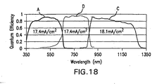
- FIG. 18 is an EQE graph of an inverted metamorphic solar cell with barrier layers according to the present invention.
- FIG. 1 depicts the multijunction solar cell according to the present invention after formation of the three subcells A, B and C on a substrate. More particularly, there is shown a substrate 101, which may be either gallium arsenide (GaAs), germanium (Ge), or other suitable material.
- a nucleation layer 102 is deposited on the substrate.
- a buffer layer 103, and an etch stop layer 104 are further deposited.
- a contact layer 105 is then deposited on layer 104, and a window layer 106 is deposited on the contact layer.
- the subcell A consisting of an n+ emitter layer 107 and a p-type base layer 108, is then deposited on the window layer 106.
- the multijunction solar cell structure could be formed by any suitable combination of group III to V elements listed in the periodic table subject to lattice constant and band gap requirements, wherein the group III includes boron (B), aluminum (Al), gallium (Ga), indium (In), and thallium (T).
- the group IV includes carbon (C), silicon (Si), germanium (Ge), and tin (Sn).
- the group V includes nitrogen (N), phosphorous (P), arsenic (As), antimony (Sb), and bismuth (Bi).
- the emitter layer 107 is composed of InQa(Al)P and the base layer is composed of InGa(Al)P.
- A1 term in parenthesis means that A1 is an optional constituent, and in this instance may be used in an amount ranging from 0% to 30%.
- BSF back surface field
- the BSF layer 109 drives minority carriers from the region near the base/BSF interface surface to minimize the effect of recombination loss.
- a BSF layer 109 reduces recombination loss at the backside of the solar subcell A and thereby reduces the recombination in the base.
- BSF layer 109 On top of the BSF layer 109 is deposited a sequence of heavily doped p-type and n-type layers 110 which forms a tunnel diode which is a circuit element to connect subcell A to subcell B.
- a window layer 111 is deposited on top of the tunnel diode layers 110 .
- the window layer 111 used in the subcell B also operates to reduce the recombination loss.
- the window layer 111 also improves the passivation of the cell surface of the underlying junctions. It should be apparent to one skilled in the art, that additional layer(s) may be added or deleted in the cell structure without departing from the scope of the present invention.
- the layers of cell B are deposited: the emitter layer 112, and the p-type base layer 113. These layers are preferably composed of InGaP and Ga(In)As respectively, although any other suitable materials consistent with lattice constant and band gap requirements may be used as well.
- a BSF layer 114 which performs the same function as the BSF layer 109.
- a p++/n++ tunnel diode 115 is deposited over the BSF layer 114 similar to the layers 110, again forming a circuit element to connect cell B to cell C.
- a barrier layer 116a preferably composed of InGa(Al)P, is deposited over the tunnel diode 115, to a thickness of about 1.0 micron.
- Such barrier layer is intended to prevent threading dislocations from propagating, either opposite to the direction of growth into the middle and top subcells B and A, or in the direction of growth into the bottom subcell C.
- the barrier layer may be any combination of III - V compound semiconductor layers having a bandgap energy greater than or equal to the grading interlayer 116, and a thickness sufficient to reduce the propagation of threading dislocations.
- Typical materials are As, P, N or Sb based III - V semiconductor materials.
- a grading interlayer or metamorphic layer 116 is deposited over the barrier layer 116a.
- Layer 116 is preferably a compositionally step-graded series of InGaAlAs layers with monotonically changing lattice constant that is intended to achieve a transition in lattice constant from subcell B to subcell C.
- the band gap of layers 116 is 1.5 eV consistent with a value slightly greater than the band gap of the middle subcell B.
- a grading interlayer may be composed of any of the As, P, N, Sb based III - V compound semiconductors subject to the constraints of having the in-plane lattice parameter greater or equal to that of the second solar cell B and less than or equal to that of the third solar cell C, and having a bandgap energy greater than that of the second solar cell B.
- the step grade contains nine compositionally graded InGaP steps with each step layer having a thickness of 0.25 micron.
- the layer 116 is composed of InGaAlAs, with monotonically changing lattice constant, over at least nine steps.
- a second barrier layer 116b is deposited over the InGaAlAs metamorphic layer 116.
- the second barrier layer 116b will have a different composition than that of barrier layer 116a, and again the base region may be GalnAs, GaAsSb, or GaInAsN.
- a window layer 117 is deposited over the barrier layer 116b, this window layer operating to reduce the recombination loss in subcell "C". It should be apparent to one skilled in the art that additional layers may be added or deleted in the cell structure without departing from the scope of the present invention.
- the layers of cell C are deposited: the n+ emitter layer 118, and the p-type base layer 119. These layers are preferably composed of InGaP and Ga(In)As respectively, although another suitable materials consistent with lattice constant and band gap requirements may be used as well.
- a BSF layer 120 is deposited on top of the cell C, the BSF layer performing the same function as the BSF layers 109 and 114.
- ap+ contact layer 121 is deposited on the BSF layer 120.
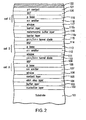
- FIG. 2 is a cross-sectional view of the solar cell of FIG. 1 after the next process step in which a metal contact layer 122 is deposited over the p+ semiconductor contact layer 121.
- the metal is preferably Ti/Au/Ag/Au.
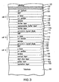
- FIG. 3 is a cross-sectional view of the solar cell of FIG. 2 after the next process step in which an adhesive layer 123 is deposited over the metal layer 122.
- the adhesive is preferably GenTak 330 (distributed by General Chemical Corp.).
- FIG. 4 is a cross-sectional view of the solar cell of FIG. 3 after the next process step in which a surrogate substrate, preferably sapphire, is attached.
- the surrogate substrate is about 40 mils in thickness, and is perforated with holes about 1mm in diameter, spaced 4mm apart, to aid in subsequent removal of the adhesive and the substrate.
- FIG. 5A is a cross-sectional view of the solar cell of FIG. 4 after the next process step in which the original substrate is removed by a sequence of lapping and/or etching steps in which the substrate 101, the buffer layer 103, and the etch stop layer 104, are removed.
- the etchant is growth substrate dependent.
- FIG. 5B is a cross-sectional view of the solar cell of FIG. 5A from the solar cell of FIG. 5A from the orientation with the surrogate substrate 124 being at the bottom of the Figure.
- FIG. 6A is a top plan view of a wafer in which the solar cells are implemented.
- each cell there are grid lines 501 (more particularly shown in cross-section in FIG. 10 ), an interconnecting bus line 502, and a contact pad 503.
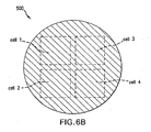
- FIG. 6B is a bottom plan view of the wafer with four solar cells shown in FIG. 6A .
- FIG. 7 is a top plan view of the wafer of FIG. 6A after the next process step in which a mesa 510 is etched around the periphery of each cell using phosphide and arsenide etchants.
- FIG. 8 is a simplified cross-sectional view of the solar cell of FIG. 5B depicting just a few of the top layers and lower layers over the surrogate substrate 124.
- FIG. 9 is a cross-sectional view of the solar cell of FIG. 8 after the next process step in which the etch stop layer 104 is removed by a HCl/H 2 O solution.
- FIG. 10 is a cross-sectional view of the solar cell of FIG. 9 after the next sequence of process steps in which a photoresist mask (not shown) is placed over the contact layer 105 to form the grid lines 501.
- the grid lines 501 are deposited via evaporation and lithographically patterned and deposited over the contact layer 105.
- the mask is lifted off to form the metal grid lines 501.
- FIG. 11 is a cross-sectional view of the solar cell of FIG. 10 after the next process step in which the grid lines are used as a mask to etch down the surface to the window layer 106 using a citric acid/peroxide etching mixture.
- FIG. 12 is a cross-sectional view of the solar cell of FIG. 11 after the next process step in which an antireflective (ARC) dielectric coating layer 130 is applied over the entire surface of the "bottom" side of the wafer with the grid lines 501.
- ARC antireflective
- FIG. 13 is a cross-sectional view of the solar cell of FIG. 12 after the next process step in which the mesa 501 is etched down to the metal layer 122 using phosphide and arsenide etchants.
- the cross-section in the figure is depicted as seen from the A-A plane shown in FIG. 7 .
- One or more silver electrodes are then welded to the contact pad(s).
- FIG. 14 is a cross-sectional view of the solar cell of FIG. 13 after the next process step after the surrogate substrate 124 and adhesive 123 are removed by EKC 922.
- the preferred perforations provided in the surrogate substrate have a diameter of 0.033 inches, and are separated by 0.152 inches.
- FIG. 15 is a cross-sectional view of the solar cell of FIG. 14 after the next process step in which an adhesive is applied over the ARC layer 130 and a coverglass attached thereto.
- FIGs. 16 through 18 Experimented indication of the efficacy of the present invention is provided in FIGs. 16 through 18 .
- External quantum efficiency (EQE) measurements were made and the results shown in FIG. 16 indicate that the long wavelength response of the middle subcell B was lower than expected.
- Nomarski microscopy indicated unexpected cross-hatching (a mode of strain relief) on the initial epitaxial layer of the lattice matched subcell A.
- Photoluminescence mapping further revealed that the luminescence of the middle subcell B was lower than expected.
- Cathodoluminescence measurements indicated that the threading dislocation density was high in the middle subcell B, but the threading dislocations did not penetrate the top subcell A. These measurements were consistent with the EQE measurements shown in FIG.
- FIG. 17 illustrates a comparison of the EQE measurements of a middle subcell in a triple junction solar cell with and without the addition of the barrier layer 116a according to the present invention.
- the graph of subcell B (without the barrier layer) has an integrated current (AMO) of 15.6 mA/cm 2 and lower EQE than that of subcell D (with the barrier layer), has an integrated current AMO) of 17.4 mA/cm 2 .
- Figure 16 is an EQE for the solar cell of FIG, 1 without a barrier layer
- Figure 18 is an EQE for the solar cell with a barrier layer.
- the current of the middle subcell B of the solar cell of Figure 18 (17.4 mA/cm 2 ) is only slightly below the current of the top subcell C (18.4 mA/cm 2 ).
- Such close current matching of the middle subcell and the top subcell demonstrates the efficacy of the present invention.
- the subcells may alternatively be contacted by means of metal contacts to laterally conductive semiconductor layers between the subcells. Such arrangements may be used to form 3-terminal, 4-terminal, and in general, n-terminal devices.
- the subcells can be interconnected in circuits using these additional terminals such that most of the available photogenerated current density in each subcell can be used effectively, leading to high efficiency for the multijunction cell, notwithstanding that the photogenerated current densities are typically different in the various subcells.
- the present invention may utilize one or more homojunction cells or subcells, i.e., a cell or subcell in which the p-n junction is formed between a p-type semiconductor and an n-type semiconductors both of which have the same chemical composition and the same band gap, differing only in the dopant species and types.
- Subcell A with p-type and n-type InGaP is one example of a homojunction subcell.
- the present invention may utilize one or more heterojunction cells or subcells, i.e., a cell or subcell in which the p-n junction is formed between a p-type semiconductor and an n-type semiconductor having different chemical compositions of the semiconductor material in the n-type and n-type regions, and/or different band gap energies in the p-type regions, in addition to utilizing different dopant species and type in the p-type and n-type regions that form the p-n junction.
- heterojunction cells or subcells i.e., a cell or subcell in which the p-n junction is formed between a p-type semiconductor and an n-type semiconductor having different chemical compositions of the semiconductor material in the n-type and n-type regions, and/or different band gap energies in the p-type regions, in addition to utilizing different dopant species and type in the p-type and n-type regions that form the p-n junction.
- the composition of the window or BSF layers may utilize other semiconductor compounds, subject to lattice constant and bandgap requirements, and may include AlInP, AlAs, AlP, AlGaInP. AlGaAsP, AlGaInAs, AlGaInPAs, OaInP, GaInAs, GaInPAs, AlGaAs, AlInAs, AlInPAs, GaAsSb, AlAsSb, GaAlAsSb, AlInSb, GaInSb, AlGaInSb, AIN, GaN, InN, GaInN, AlGaInN, GaInNAs, AlGaInNAs, ZnSSe, CdSSe, and similar materials, and still fall within the scope of the present invention.
Landscapes
- Engineering & Computer Science (AREA)
- Life Sciences & Earth Sciences (AREA)
- Physics & Mathematics (AREA)
- Sustainable Energy (AREA)
- Condensed Matter Physics & Semiconductors (AREA)
- Electromagnetism (AREA)
- General Physics & Mathematics (AREA)
- Computer Hardware Design (AREA)
- Microelectronics & Electronic Packaging (AREA)
- Power Engineering (AREA)
- Sustainable Development (AREA)
- Chemical & Material Sciences (AREA)
- Crystallography & Structural Chemistry (AREA)
- Manufacturing & Machinery (AREA)
- Photovoltaic Devices (AREA)
Claims (20)
- Procédé de formation d'une cellule solaire à jonctions multiples comprenant une sous-cellule supérieure (C), une sous-cellule médiane (B) et une sous-cellule inférieure (A), le procédé consistant à, dans l'ordre suivant :fournir un premier substrat (101) pour la croissance épitaxiale d'un matériau semiconducteur ;former une première sous-cellule solaire (A) sur ledit substrat ayant une première bande interdite ;former une seconde sous-cellule solaire (B) sur ladite première sous-cellule solaire (A) ayant une seconde bande interdite inférieure à ladite première bande interdite ;former une première couche barrière (116a) sur ladite seconde sous-cellule (B) ;former une intercouche de gradation (116) sur ladite couche barrière (116a), ladite intercouche de gradation (116) ayant une troisième bande interdite supérieure à ladite seconde bande interdite ;former une seconde couche barrière (116b) sur ladite intercouche de gradation (116) ; etformer une troisième sous-cellule solaire (C) sur ladite intercouche de gradation (116) ayant une quatrième bande interdite inférieure à ladite seconde bande interdite de façon que ladite troisième sous-cellule (C) présente une désadaptation de réseau par rapport à ladite seconde sous-cellule (B),caractérisé en ce quelesdites première (116a) et seconde (116b) couches barrières sont composées de semiconducteurs composites quelconques de type III-V à base d'As, P, N ou Sb, ladite seconde couche barrière (116b) ayant une composition différente de ladite première couche barrière (116a) ; etlesdites première (116a) et seconde (116b) couches barrières sont composées d'un matériau approprié et ont une constante de réseau permettant d'éviter la propagation de dislocations émergentes.
- Procédé selon la revendication 1, dans lequel ladite première couche barrière (116a) a une énergie de bande interdite supérieure ou égale à celle de l'intercouche de gradation.
- Procédé selon la revendication 1, dans lequel ladite seconde couche barrière (116b) a une énergie de bande interdite supérieure ou égale à celle de la première intercouche de gradation (116a).
- Procédé selon la revendication 1, dans lequel ledit premier substrat (101) est sélectionné dans le groupe constitué du germanium ou du GaAs.
- Procédé selon la revendication 1, dans lequel ladite première sous-cellule solaire (A) est composée d'une région d'émetteur d'InGa(Al)P et d'une région de base d'InGa(Al)P.
- Procédé selon la revendication 5, dans lequel ladite seconde cellule solaire (B) est composée d'une région d'émetteur de GaInP, de GaInAs, de GaAsSb ou de GaInAsN et d'une région de base de GaInAs, de GaAsSb ou de GaInAsN.
- Procédé selon la revendication 1, dans lequel ladite intercouche de gradation (116) est composée de l'un quelconque des semiconducteurs composites III-V à base d'As, P, N, Sb soumis aux contraintes consistant à avoir un paramètre de réseau dans le plan supérieur ou égal à celui de la seconde cellule solaire (B) et inférieur ou égal à celui de la troisième cellule solaire (C), et ayant une énergie de bande interdite supérieure à celle de la seconde cellule solaire (B).
- Procédé selon la revendication 5, dans lequel ladite seconde sous-cellule solaire (B) est composée d'une région d'émetteur d'InGaP et d'une région de base de GaAs.
- Procédé selon la revendication 1, dans lequel ladite intercouche de gradation (116) est composée d'InGaAlAs.
- Procédé selon la revendication 7, dans lequel ladite intercouche de gradation (116) est composée de neuf gradins de couches ayant des constantes de réseau variant de manière monotone.
- Procédé selon la revendication 1, consistant en outre à déposer une couche de contact (121) sur ladite troisième sous-cellule solaire (C) et à établir un contact électrique avec celle-ci.
- Procédé selon la revendication 9, consistant en outre à fixer un second substrat de substitution (124) sur ladite couche de contact (121) et à enlever le premier substrat (101).
- Procédé selon la revendication 1, consistant en outre à :mettre sous la forme d'un motif de grille une couche de contact (105) ; etgraver un puits le long de la périphérie de ladite cellule solaire de façon à former une structure de mesa sur ledit second substrat de substitution (124).
- Cellule solaire à jonctions multiples comprenant :un substrat (101) ;une première sous-cellule solaire (A) sur ledit substrat (101) ayant une première bande interdite ;une seconde sous-cellule solaire (B) disposée sur ladite première sous-cellule (A) et ayant une seconde bande interdite inférieure à ladite première bande interdite ;une première couche barrière (116a) disposée sur ladite seconde sous-cellule (B) ;une intercouche de gradation (116) disposée sur ladite première couche barrière (116a) et ayant une troisième bande interdite supérieure à ladite seconde bande interdite ;une seconde couche barrière (116b) sur ladite intercouche de gradation (116) ; etune troisième sous-cellule solaire (C) disposée sur ladite intercouche de gradation (116) qui présente une désadaptation de réseau par rapport à ladite seconde sous-cellule (B) et ayant une quatrième bande interdite inférieure à ladite seconde bande interdite, ladite cellule solaire étant caractérisée en ce que :lesdites première (116a) et seconde (116b) couches barrières sont composées de semiconducteurs composites quelconques de type III-V à base d'As, P, N ou Sb, ladite seconde couche barrière (116b) ayant une composition différente de celle de ladite première couche barrière (116a) ; etlesdites première (116a) et seconde (116b) couches barrières sont composées d'un matériau approprié et ont une constante de réseau empêchant la propagation de dislocations émergentes.
- Cellule solaire selon la revendication 14, dans laquelle ladite couche barrière (116a) a une énergie de bande interdite supérieure ou égale à celle de l'intercouche de gradation (116).
- Cellule solaire selon la revendication 14, dans laquelle ladite seconde couche barrière (116b) a une énergie de bande interdite supérieure ou égale à celle de l'intercouche de gradation (116).
- Cellule solaire selon la revendication 14, dans laquelle ledit substrat (101) est sélectionné dans le groupe constitué du germanium ou du GaAs.
- Cellule solaire selon la revendication 14, dans laquelle ladite première sous-cellule solaire (A) est composée d'InGa(Al)P.
- Cellule solaire selon la revendication 14, dans laquelle ladite seconde sous-cellule solaire (B) est composée d'une région d'émetteur de GaInP, de GaInAs, de GaAsSb ou de GaInAsN et d'une région de base de GaInAs, de GaAsSb ou de GaInAsN.
- Cellule solaire selon la revendication 14, dans laquelle ladite troisième sous-cellule solaire (C) est composée d'InGaAs.
Priority Applications (2)
| Application Number | Priority Date | Filing Date | Title |
|---|---|---|---|
| AT08013467T ATE511704T1 (de) | 2008-07-25 | 2008-07-25 | Sperrschichten in umgekehrten metamorphischen multiverbindungssolarzellen |
| EP08013467A EP2148378B1 (fr) | 2008-07-25 | 2008-07-25 | Couches barrière dans des cellules solaires métamorphiques multijonctions inversées |
Applications Claiming Priority (1)
| Application Number | Priority Date | Filing Date | Title |
|---|---|---|---|
| EP08013467A EP2148378B1 (fr) | 2008-07-25 | 2008-07-25 | Couches barrière dans des cellules solaires métamorphiques multijonctions inversées |
Publications (2)
| Publication Number | Publication Date |
|---|---|
| EP2148378A1 EP2148378A1 (fr) | 2010-01-27 |
| EP2148378B1 true EP2148378B1 (fr) | 2011-06-01 |
Family
ID=40158597
Family Applications (1)
| Application Number | Title | Priority Date | Filing Date |
|---|---|---|---|
| EP08013467A Revoked EP2148378B1 (fr) | 2008-07-25 | 2008-07-25 | Couches barrière dans des cellules solaires métamorphiques multijonctions inversées |
Country Status (2)
| Country | Link |
|---|---|
| EP (1) | EP2148378B1 (fr) |
| AT (1) | ATE511704T1 (fr) |
Families Citing this family (2)
| Publication number | Priority date | Publication date | Assignee | Title |
|---|---|---|---|---|
| CN113644147A (zh) * | 2021-06-25 | 2021-11-12 | 北京空间飞行器总体设计部 | 一种与火星光谱匹配的三结砷化镓太阳电池 |
| CN114335215B (zh) * | 2022-03-15 | 2022-06-14 | 南昌凯迅光电股份有限公司 | 一种带有渐变隧穿结的砷化镓太阳电池及其制作方法 |
Family Cites Families (3)
| Publication number | Priority date | Publication date | Assignee | Title |
|---|---|---|---|---|
| WO2004054003A1 (fr) * | 2002-12-05 | 2004-06-24 | Blue Photonics, Inc. | Piles solaires multijonctions, monolithiques, a efficacite elevee, contenant des materiaux a reseaux non apparies et procedes de formation associes |
| US8536445B2 (en) * | 2006-06-02 | 2013-09-17 | Emcore Solar Power, Inc. | Inverted metamorphic multijunction solar cells |
| US20080245409A1 (en) * | 2006-12-27 | 2008-10-09 | Emcore Corporation | Inverted Metamorphic Solar Cell Mounted on Flexible Film |
-
2008
- 2008-07-25 AT AT08013467T patent/ATE511704T1/de not_active IP Right Cessation
- 2008-07-25 EP EP08013467A patent/EP2148378B1/fr not_active Revoked
Also Published As
| Publication number | Publication date |
|---|---|
| EP2148378A1 (fr) | 2010-01-27 |
| ATE511704T1 (de) | 2011-06-15 |
Similar Documents
| Publication | Publication Date | Title |
|---|---|---|
| JP6194283B2 (ja) | 多接合ソーラーセル及びその形成方法 | |
| US8039291B2 (en) | Demounting of inverted metamorphic multijunction solar cells | |
| EP2086024B1 (fr) | Sous-cellules d'hétérojonction dans des cellules solaires multi-jonctions inversées métamorphiques | |
| US9691929B2 (en) | Four junction inverted metamorphic multijunction solar cell with two metamorphic layers | |
| US8236600B2 (en) | Joining method for preparing an inverted metamorphic multijunction solar cell | |
| US8969712B2 (en) | Four junction inverted metamorphic multijunction solar cell with a single metamorphic layer | |
| US20090288703A1 (en) | Wide Band Gap Window Layers In Inverted Metamorphic Multijunction Solar Cells | |
| US20090078311A1 (en) | Surfactant Assisted Growth in Barrier Layers In Inverted Metamorphic Multijunction Solar Cells | |
| US7960201B2 (en) | String interconnection and fabrication of inverted metamorphic multijunction solar cells | |
| US20090229658A1 (en) | Non-Isoelectronic Surfactant Assisted Growth In Inverted Metamorphic Multijunction Solar Cells | |
| US20100012174A1 (en) | High band gap contact layer in inverted metamorphic multijunction solar cells | |
| US20090272438A1 (en) | Strain Balanced Multiple Quantum Well Subcell In Inverted Metamorphic Multijunction Solar Cell | |
| US20090229662A1 (en) | Off-Cut Substrates In Inverted Metamorphic Multijunction Solar Cells | |
| US20150340530A1 (en) | Back metal layers in inverted metamorphic multijunction solar cells | |
| US20090272430A1 (en) | Refractive Index Matching in Inverted Metamorphic Multijunction Solar Cells | |
| US20140342494A1 (en) | Ohmic n-contact formed at low temperature in inverted metamorphic multijunction solar cells | |
| US20100206365A1 (en) | Inverted Metamorphic Multijunction Solar Cells on Low Density Carriers | |
| US20120211047A1 (en) | String interconnection of inverted metamorphic multijunction solar cells on flexible perforated carriers | |
| US20100229913A1 (en) | Contact Layout and String Interconnection of Inverted Metamorphic Multijunction Solar Cells | |
| US20100122764A1 (en) | Surrogate Substrates for Inverted Metamorphic Multijunction Solar Cells | |
| US10541349B1 (en) | Methods of forming inverted multijunction solar cells with distributed Bragg reflector | |
| EP2148378B1 (fr) | Couches barrière dans des cellules solaires métamorphiques multijonctions inversées | |
| US10170656B2 (en) | Inverted metamorphic multijunction solar cell with a single metamorphic layer |
Legal Events
| Date | Code | Title | Description |
|---|---|---|---|
| PUAI | Public reference made under article 153(3) epc to a published international application that has entered the european phase |
Free format text: ORIGINAL CODE: 0009012 |
|
| AK | Designated contracting states |
Kind code of ref document: A1 Designated state(s): AT BE BG CH CY CZ DE DK EE ES FI FR GB GR HR HU IE IS IT LI LT LU LV MC MT NL NO PL PT RO SE SI SK TR |
|
| AX | Request for extension of the european patent |
Extension state: AL BA MK RS |
|
| 17P | Request for examination filed |
Effective date: 20100611 |
|
| 17Q | First examination report despatched |
Effective date: 20100705 |
|
| AKX | Designation fees paid |
Designated state(s): AT BE BG CH CY CZ DE DK EE ES FI FR GB GR HR HU IE IS IT LI LT LU LV MC MT NL NO PL PT RO SE SI SK TR |
|
| GRAP | Despatch of communication of intention to grant a patent |
Free format text: ORIGINAL CODE: EPIDOSNIGR1 |
|
| GRAS | Grant fee paid |
Free format text: ORIGINAL CODE: EPIDOSNIGR3 |
|
| GRAA | (expected) grant |
Free format text: ORIGINAL CODE: 0009210 |
|
| AK | Designated contracting states |
Kind code of ref document: B1 Designated state(s): AT BE BG CH CY CZ DE DK EE ES FI FR GB GR HR HU IE IS IT LI LT LU LV MC MT NL NO PL PT RO SE SI SK TR |
|
| REG | Reference to a national code |
Ref country code: GB Ref legal event code: FG4D |
|
| REG | Reference to a national code |
Ref country code: CH Ref legal event code: EP |
|
| REG | Reference to a national code |
Ref country code: IE Ref legal event code: FG4D |
|
| REG | Reference to a national code |
Ref country code: DE Ref legal event code: R096 Ref document number: 602008007332 Country of ref document: DE Effective date: 20110714 |
|
| REG | Reference to a national code |
Ref country code: NL Ref legal event code: VDEP Effective date: 20110601 |
|
| PG25 | Lapsed in a contracting state [announced via postgrant information from national office to epo] |
Ref country code: SE Free format text: LAPSE BECAUSE OF FAILURE TO SUBMIT A TRANSLATION OF THE DESCRIPTION OR TO PAY THE FEE WITHIN THE PRESCRIBED TIME-LIMIT Effective date: 20110601 Ref country code: HR Free format text: LAPSE BECAUSE OF FAILURE TO SUBMIT A TRANSLATION OF THE DESCRIPTION OR TO PAY THE FEE WITHIN THE PRESCRIBED TIME-LIMIT Effective date: 20110601 Ref country code: NO Free format text: LAPSE BECAUSE OF FAILURE TO SUBMIT A TRANSLATION OF THE DESCRIPTION OR TO PAY THE FEE WITHIN THE PRESCRIBED TIME-LIMIT Effective date: 20110901 Ref country code: LT Free format text: LAPSE BECAUSE OF FAILURE TO SUBMIT A TRANSLATION OF THE DESCRIPTION OR TO PAY THE FEE WITHIN THE PRESCRIBED TIME-LIMIT Effective date: 20110601 |
|
| PG25 | Lapsed in a contracting state [announced via postgrant information from national office to epo] |
Ref country code: CY Free format text: LAPSE BECAUSE OF FAILURE TO SUBMIT A TRANSLATION OF THE DESCRIPTION OR TO PAY THE FEE WITHIN THE PRESCRIBED TIME-LIMIT Effective date: 20110601 Ref country code: ES Free format text: LAPSE BECAUSE OF FAILURE TO SUBMIT A TRANSLATION OF THE DESCRIPTION OR TO PAY THE FEE WITHIN THE PRESCRIBED TIME-LIMIT Effective date: 20110912 Ref country code: AT Free format text: LAPSE BECAUSE OF FAILURE TO SUBMIT A TRANSLATION OF THE DESCRIPTION OR TO PAY THE FEE WITHIN THE PRESCRIBED TIME-LIMIT Effective date: 20110601 Ref country code: LV Free format text: LAPSE BECAUSE OF FAILURE TO SUBMIT A TRANSLATION OF THE DESCRIPTION OR TO PAY THE FEE WITHIN THE PRESCRIBED TIME-LIMIT Effective date: 20110601 Ref country code: FI Free format text: LAPSE BECAUSE OF FAILURE TO SUBMIT A TRANSLATION OF THE DESCRIPTION OR TO PAY THE FEE WITHIN THE PRESCRIBED TIME-LIMIT Effective date: 20110601 Ref country code: GR Free format text: LAPSE BECAUSE OF FAILURE TO SUBMIT A TRANSLATION OF THE DESCRIPTION OR TO PAY THE FEE WITHIN THE PRESCRIBED TIME-LIMIT Effective date: 20110902 Ref country code: SI Free format text: LAPSE BECAUSE OF FAILURE TO SUBMIT A TRANSLATION OF THE DESCRIPTION OR TO PAY THE FEE WITHIN THE PRESCRIBED TIME-LIMIT Effective date: 20110601 |
|
| PG25 | Lapsed in a contracting state [announced via postgrant information from national office to epo] |
Ref country code: MT Free format text: LAPSE BECAUSE OF FAILURE TO SUBMIT A TRANSLATION OF THE DESCRIPTION OR TO PAY THE FEE WITHIN THE PRESCRIBED TIME-LIMIT Effective date: 20110601 Ref country code: BE Free format text: LAPSE BECAUSE OF FAILURE TO SUBMIT A TRANSLATION OF THE DESCRIPTION OR TO PAY THE FEE WITHIN THE PRESCRIBED TIME-LIMIT Effective date: 20110601 Ref country code: NL Free format text: LAPSE BECAUSE OF FAILURE TO SUBMIT A TRANSLATION OF THE DESCRIPTION OR TO PAY THE FEE WITHIN THE PRESCRIBED TIME-LIMIT Effective date: 20110601 |
|
| PG25 | Lapsed in a contracting state [announced via postgrant information from national office to epo] |
Ref country code: CZ Free format text: LAPSE BECAUSE OF FAILURE TO SUBMIT A TRANSLATION OF THE DESCRIPTION OR TO PAY THE FEE WITHIN THE PRESCRIBED TIME-LIMIT Effective date: 20110601 Ref country code: IS Free format text: LAPSE BECAUSE OF FAILURE TO SUBMIT A TRANSLATION OF THE DESCRIPTION OR TO PAY THE FEE WITHIN THE PRESCRIBED TIME-LIMIT Effective date: 20111001 Ref country code: EE Free format text: LAPSE BECAUSE OF FAILURE TO SUBMIT A TRANSLATION OF THE DESCRIPTION OR TO PAY THE FEE WITHIN THE PRESCRIBED TIME-LIMIT Effective date: 20110601 Ref country code: PT Free format text: LAPSE BECAUSE OF FAILURE TO SUBMIT A TRANSLATION OF THE DESCRIPTION OR TO PAY THE FEE WITHIN THE PRESCRIBED TIME-LIMIT Effective date: 20111003 |
|
| PG25 | Lapsed in a contracting state [announced via postgrant information from national office to epo] |
Ref country code: MC Free format text: LAPSE BECAUSE OF NON-PAYMENT OF DUE FEES Effective date: 20110731 Ref country code: PL Free format text: LAPSE BECAUSE OF FAILURE TO SUBMIT A TRANSLATION OF THE DESCRIPTION OR TO PAY THE FEE WITHIN THE PRESCRIBED TIME-LIMIT Effective date: 20110601 Ref country code: RO Free format text: LAPSE BECAUSE OF FAILURE TO SUBMIT A TRANSLATION OF THE DESCRIPTION OR TO PAY THE FEE WITHIN THE PRESCRIBED TIME-LIMIT Effective date: 20110601 Ref country code: SK Free format text: LAPSE BECAUSE OF FAILURE TO SUBMIT A TRANSLATION OF THE DESCRIPTION OR TO PAY THE FEE WITHIN THE PRESCRIBED TIME-LIMIT Effective date: 20110601 |
|
| PLAZ | Examination of admissibility of opposition: despatch of communication + time limit |
Free format text: ORIGINAL CODE: EPIDOSNOPE2 |
|
| PLBI | Opposition filed |
Free format text: ORIGINAL CODE: 0009260 |
|
| PLBA | Examination of admissibility of opposition: reply received |
Free format text: ORIGINAL CODE: EPIDOSNOPE4 |
|
| PLAX | Notice of opposition and request to file observation + time limit sent |
Free format text: ORIGINAL CODE: EPIDOSNOBS2 |
|
| 26 | Opposition filed |
Opponent name: AZUR SPACE SOLAR POWER GMBH Effective date: 20120301 |
|
| REG | Reference to a national code |
Ref country code: IE Ref legal event code: MM4A |
|
| REG | Reference to a national code |
Ref country code: DE Ref legal event code: R026 Ref document number: 602008007332 Country of ref document: DE Effective date: 20120301 |
|
| PG25 | Lapsed in a contracting state [announced via postgrant information from national office to epo] |
Ref country code: DK Free format text: LAPSE BECAUSE OF FAILURE TO SUBMIT A TRANSLATION OF THE DESCRIPTION OR TO PAY THE FEE WITHIN THE PRESCRIBED TIME-LIMIT Effective date: 20110601 |
|
| PG25 | Lapsed in a contracting state [announced via postgrant information from national office to epo] |
Ref country code: IE Free format text: LAPSE BECAUSE OF NON-PAYMENT OF DUE FEES Effective date: 20110725 |
|
| PLBB | Reply of patent proprietor to notice(s) of opposition received |
Free format text: ORIGINAL CODE: EPIDOSNOBS3 |
|
| REG | Reference to a national code |
Ref country code: CH Ref legal event code: PL |
|
| GBPC | Gb: european patent ceased through non-payment of renewal fee |
Effective date: 20120725 |
|
| PG25 | Lapsed in a contracting state [announced via postgrant information from national office to epo] |
Ref country code: CH Free format text: LAPSE BECAUSE OF NON-PAYMENT OF DUE FEES Effective date: 20120731 Ref country code: LI Free format text: LAPSE BECAUSE OF NON-PAYMENT OF DUE FEES Effective date: 20120731 Ref country code: GB Free format text: LAPSE BECAUSE OF NON-PAYMENT OF DUE FEES Effective date: 20120725 |
|
| PG25 | Lapsed in a contracting state [announced via postgrant information from national office to epo] |
Ref country code: LU Free format text: LAPSE BECAUSE OF NON-PAYMENT OF DUE FEES Effective date: 20110725 |
|
| PG25 | Lapsed in a contracting state [announced via postgrant information from national office to epo] |
Ref country code: BG Free format text: LAPSE BECAUSE OF FAILURE TO SUBMIT A TRANSLATION OF THE DESCRIPTION OR TO PAY THE FEE WITHIN THE PRESCRIBED TIME-LIMIT Effective date: 20110901 |
|
| PG25 | Lapsed in a contracting state [announced via postgrant information from national office to epo] |
Ref country code: TR Free format text: LAPSE BECAUSE OF FAILURE TO SUBMIT A TRANSLATION OF THE DESCRIPTION OR TO PAY THE FEE WITHIN THE PRESCRIBED TIME-LIMIT Effective date: 20110601 |
|
| PG25 | Lapsed in a contracting state [announced via postgrant information from national office to epo] |
Ref country code: HU Free format text: LAPSE BECAUSE OF FAILURE TO SUBMIT A TRANSLATION OF THE DESCRIPTION OR TO PAY THE FEE WITHIN THE PRESCRIBED TIME-LIMIT Effective date: 20110601 |
|
| APAH | Appeal reference modified |
Free format text: ORIGINAL CODE: EPIDOSCREFNO |
|
| APBM | Appeal reference recorded |
Free format text: ORIGINAL CODE: EPIDOSNREFNO |
|
| APBP | Date of receipt of notice of appeal recorded |
Free format text: ORIGINAL CODE: EPIDOSNNOA2O |
|
| APAL | Date of receipt of statement of grounds of an appeal modified |
Free format text: ORIGINAL CODE: EPIDOSCNOA3O |
|
| APBQ | Date of receipt of statement of grounds of appeal recorded |
Free format text: ORIGINAL CODE: EPIDOSNNOA3O |
|
| REG | Reference to a national code |
Ref country code: FR Ref legal event code: TP Owner name: SOLAERO TECHNOLOGIES CORP., US Effective date: 20150323 |
|
| RAP2 | Party data changed (patent owner data changed or rights of a patent transferred) |
Owner name: SOLAERO TECHNOLOGIES CORP. |
|
| REG | Reference to a national code |
Ref country code: FR Ref legal event code: PLFP Year of fee payment: 9 |
|
| REG | Reference to a national code |
Ref country code: FR Ref legal event code: PLFP Year of fee payment: 10 |
|
| REG | Reference to a national code |
Ref country code: FR Ref legal event code: PLFP Year of fee payment: 11 |
|
| PGFP | Annual fee paid to national office [announced via postgrant information from national office to epo] |
Ref country code: FR Payment date: 20180612 Year of fee payment: 11 |
|
| REG | Reference to a national code |
Ref country code: DE Ref legal event code: R064 Ref document number: 602008007332 Country of ref document: DE Ref country code: DE Ref legal event code: R103 Ref document number: 602008007332 Country of ref document: DE |
|
| APBU | Appeal procedure closed |
Free format text: ORIGINAL CODE: EPIDOSNNOA9O |
|
| RDAF | Communication despatched that patent is revoked |
Free format text: ORIGINAL CODE: EPIDOSNREV1 |
|
| STAA | Information on the status of an ep patent application or granted ep patent |
Free format text: STATUS: PATENT REVOKED |
|
| RDAG | Patent revoked |
Free format text: ORIGINAL CODE: 0009271 |
|
| STAA | Information on the status of an ep patent application or granted ep patent |
Free format text: STATUS: PATENT REVOKED |
|
| PGFP | Annual fee paid to national office [announced via postgrant information from national office to epo] |
Ref country code: DE Payment date: 20180710 Year of fee payment: 11 Ref country code: IT Payment date: 20180713 Year of fee payment: 11 |
|
| 27W | Patent revoked |
Effective date: 20180906 |