EP2147459B1 - Lamp comprising electrodeless bulb and ceramic waveguide - Google Patents
Lamp comprising electrodeless bulb and ceramic waveguide Download PDFInfo
- Publication number
- EP2147459B1 EP2147459B1 EP08750591A EP08750591A EP2147459B1 EP 2147459 B1 EP2147459 B1 EP 2147459B1 EP 08750591 A EP08750591 A EP 08750591A EP 08750591 A EP08750591 A EP 08750591A EP 2147459 B1 EP2147459 B1 EP 2147459B1
- Authority
- EP
- European Patent Office
- Prior art keywords
- lamp
- bulb
- reduced cross
- main portion
- section
- Prior art date
- Legal status (The legal status is an assumption and is not a legal conclusion. Google has not performed a legal analysis and makes no representation as to the accuracy of the status listed.)
- Not-in-force
Links
- 239000000919 ceramic Substances 0.000 title claims description 9
- 229910001507 metal halide Inorganic materials 0.000 claims abstract description 5
- 150000005309 metal halides Chemical class 0.000 claims abstract description 5
- VYPSYNLAJGMNEJ-UHFFFAOYSA-N silicon dioxide Inorganic materials O=[Si]=O VYPSYNLAJGMNEJ-UHFFFAOYSA-N 0.000 claims abstract description 5
- JKNHZOAONLKYQL-UHFFFAOYSA-K tribromoindigane Chemical compound Br[In](Br)Br JKNHZOAONLKYQL-UHFFFAOYSA-K 0.000 claims abstract description 5
- 229910052724 xenon Inorganic materials 0.000 claims abstract description 5
- FHNFHKCVQCLJFQ-UHFFFAOYSA-N xenon atom Chemical compound [Xe] FHNFHKCVQCLJFQ-UHFFFAOYSA-N 0.000 claims abstract description 5
- 239000010453 quartz Substances 0.000 claims abstract description 4
- 230000005284 excitation Effects 0.000 claims description 4
- 229910052756 noble gas Inorganic materials 0.000 claims description 3
- 229910010293 ceramic material Inorganic materials 0.000 claims description 2
- 229910052743 krypton Inorganic materials 0.000 claims description 2
- DNNSSWSSYDEUBZ-UHFFFAOYSA-N krypton atom Chemical compound [Kr] DNNSSWSSYDEUBZ-UHFFFAOYSA-N 0.000 claims description 2
- 230000003287 optical effect Effects 0.000 claims 1
- 239000007787 solid Substances 0.000 abstract description 2
- 238000001228 spectrum Methods 0.000 abstract description 2
- 239000000463 material Substances 0.000 description 6
- 239000007789 gas Substances 0.000 description 2
- 238000004519 manufacturing process Methods 0.000 description 2
- 239000011800 void material Substances 0.000 description 2
- 229910017083 AlN Inorganic materials 0.000 description 1
- PIGFYZPCRLYGLF-UHFFFAOYSA-N Aluminum nitride Chemical compound [Al]#N PIGFYZPCRLYGLF-UHFFFAOYSA-N 0.000 description 1
- 239000004411 aluminium Substances 0.000 description 1
- 229910052782 aluminium Inorganic materials 0.000 description 1
- XAGFODPZIPBFFR-UHFFFAOYSA-N aluminium Chemical compound [Al] XAGFODPZIPBFFR-UHFFFAOYSA-N 0.000 description 1
- PNEYBMLMFCGWSK-UHFFFAOYSA-N aluminium oxide Inorganic materials [O-2].[O-2].[O-2].[Al+3].[Al+3] PNEYBMLMFCGWSK-UHFFFAOYSA-N 0.000 description 1
- 230000008878 coupling Effects 0.000 description 1
- 238000010168 coupling process Methods 0.000 description 1
- 238000005859 coupling reaction Methods 0.000 description 1
- 239000002223 garnet Substances 0.000 description 1
- 239000011261 inert gas Substances 0.000 description 1
- 229910052751 metal Inorganic materials 0.000 description 1
- 239000002184 metal Substances 0.000 description 1
- 238000000034 method Methods 0.000 description 1
- 239000008188 pellet Substances 0.000 description 1
- 229910052594 sapphire Inorganic materials 0.000 description 1
- 239000010980 sapphire Substances 0.000 description 1
- 238000007789 sealing Methods 0.000 description 1
- 239000000126 substance Substances 0.000 description 1
- 229910052727 yttrium Inorganic materials 0.000 description 1
- VWQVUPCCIRVNHF-UHFFFAOYSA-N yttrium atom Chemical compound [Y] VWQVUPCCIRVNHF-UHFFFAOYSA-N 0.000 description 1
Images
Classifications
-
- H—ELECTRICITY
- H01—ELECTRIC ELEMENTS
- H01J—ELECTRIC DISCHARGE TUBES OR DISCHARGE LAMPS
- H01J65/00—Lamps without any electrode inside the vessel; Lamps with at least one main electrode outside the vessel
- H01J65/04—Lamps in which a gas filling is excited to luminesce by an external electromagnetic field or by external corpuscular radiation, e.g. for indicating plasma display panels
- H01J65/042—Lamps in which a gas filling is excited to luminesce by an external electromagnetic field or by external corpuscular radiation, e.g. for indicating plasma display panels by an external electromagnetic field
- H01J65/044—Lamps in which a gas filling is excited to luminesce by an external electromagnetic field or by external corpuscular radiation, e.g. for indicating plasma display panels by an external electromagnetic field the field being produced by a separate microwave unit
-
- H—ELECTRICITY
- H01—ELECTRIC ELEMENTS
- H01J—ELECTRIC DISCHARGE TUBES OR DISCHARGE LAMPS
- H01J61/00—Gas-discharge or vapour-discharge lamps
- H01J61/02—Details
- H01J61/30—Vessels; Containers
- H01J61/33—Special shape of cross-section, e.g. for producing cool spot
Definitions
- the present invention relates to an electrodeless lamp.
- the bulb is back filled with inert gas.
- JP 10 106 508 in the name of New Japan Radio Co Ltd, teaches a lamp comprising in combination and electrodeless bulb, a wave guide and a microwave radiator from which microwave energy is transferred via the wave guide to the bulb for its light emitting excitation in use.
- the electrodeless bulb comprises a hollow tube sealed at both ends so as to encapsulate a light emitting material.
- the bulb has a so called main portion which is described and a "light emission part" and a reduced cross-sectional end portion, which is described as the "coupling part".
- the object of the present invention is to provide an improved electrodeless lamp.
- a lamp comprising in combination:
- both the main portion and the end portions will have circular cross-sections, where their cross-sections will be circular and the respective dimensions diameters.
- the reduced diameter portion can be tapered down in diameter from the main portion; preferably it is stepped down in diameter from the main portion.
- the reduced diameter portion can have a different shape, such as conical, it is preferably of constant cross-section, i.e. parallel sided.
- the actual distal end can be flat or domed, with its shape being chosen in accordance with the desired pattern of light distribution from it.
- the reduced diameter end portion can be three dimensionally curved, for instance ellipsoidal or paraboloidal.
- the reduction in diameter can be between 90% and 50%, preferably the stepped end will be between 4 and 5 sixths of the diameter of the main portion of the bulb.
- the reduced diameter end can have the same wall thickness as the full diameter portion, in the preferred embodiment, the interior of the bulb is of constant diameter throughout its length.
- the bulb has a location leg or stem extending from its full diameter end.
- the bulb can be of quartz as in our existing bulb, it can also be of ceramic material, such as alumina, aluminium nitride, yttrium aluminium garnet and artificial sapphire
- the charge is of metal halide and noble gas and this is normally indium bromide and xenon or krypton. Nevertheless, other volatile substances that are known to emit light when excited as a plasma can be used.
- a reflector is positioned on the ceramic waveguide.
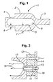
- an electrodeless bulb 1 has a hollow quartz tube 2, with a solid stem 3 extending from one end and a short hollow tip 4 extending from the other end.
- the hollow interior 5 of the tube extends into the tip 4 with the same diameter as in the tube 2, in other words the wall thickness 6 of the tip is reduced from that 7 of the main tube 2.
- the bulb is charged with an amount 8 of indium bromide and traces of other metal halides to adjust light spectrum and a filling of xenon gas.
- the bulb In use the bulb is installed in a bore 11 in a ceramic wave guide 12 with a microwave feed 14. The stem 3 is received in a bore 15 in a metal backing plate 16. On microwave excitation of the bulb, a plasma forms in the xenon, which causes the indium bromide to vaporise and emit light.
- a plasma discharge lamp such as our electrodeless bulb
- the material will tend to condense on the coolest part of the bulb.
- This condensate provides a reserve of the material.
- the condensate forms at a point where light is being emitted.
- Typical dimensions of the bulb are: Diameter of main tube 2: 6.0mm Diameter of tip 4: 5.0mm Length of tube 2: 10.0mm Length of tip 4: 5.0mm Diameter of the stem 3 2.0mm Length of stem 3: 10.0mm.
- the above described preferred bulb has been formed by grinding the outer profile of the bulb and resulting in a reduced wall thickness, we now believe that the thermal performance of the bulb can be enhanced by reducing the wall thickness 7 of the main part of the bulb to that 6 of the tip, i.e. by providing the interior wide in the main part and narrow at the stepped end. Further in production, we anticipate that the bulbs will be blown in a mould.
Landscapes
- Physics & Mathematics (AREA)
- Electromagnetism (AREA)
- Engineering & Computer Science (AREA)
- Plasma & Fusion (AREA)
- Discharge Lamps And Accessories Thereof (AREA)
- Non-Portable Lighting Devices Or Systems Thereof (AREA)
- Vessels And Coating Films For Discharge Lamps (AREA)
- Circuit Arrangements For Discharge Lamps (AREA)
Abstract
Description
- The present invention relates to an electrodeless lamp.
- In our International Patent Application No
PCT/GB05/005080, dated 23rd December 2005 WO 2006/070190 , we have described and claimed a method of making an electrodeless bulb, the method comprising the steps of: - providing a bulb enclosure of quartz glass,
- forming an adjacent neck having a bore less than a transverse internal dimension of the bulb enclosure either:
- integrally with the bulb enclosure or
- in a branch tube opening into the bulb enclosure,
- inserting at least one pellet of excitable material into the bulb enclosure through the adjacent neck,
- evacuating the bulb enclosure through the adjacent neck and
- sealing the bulb.
- Normally the bulb is back filled with inert gas.
- In addition, in our International Patent Application No.
PCT/GB2006/002018 dated 2nd June 2006 WO 2006/129102 , we have described a lamp having an electrodeless bulb, the lamp comprising: - a drive device adapted to drive at least two antenna;
- a ceramic wave guide;
- at least two respective voids receiving the said antenna in the wave guide; and
- a central void in the wave guide, for receiving the bulb, equally spaced from the antenna voids, the central void having:
- a physical opening through which light can pass from the bulb and out of the wave guide.
-
JP 10 106 508 - The object of the present invention is to provide an improved electrodeless lamp.
- According to the invention there is provided a lamp comprising in combination:
- an electrodeless bulb the bulb having:
- a main portion and
- a reduced cross-sectional dimension light emitting end portion and
- a wave guide having
- a microwave radiator
- the wave guide is a ceramic wave guide having:
- a bore for receiving the main portion of the bulb and
- the microwave radiator positioned within the waveguide and from which microwave energy is transferred via the waveguide to the bulb for its light emitting excitation in use,
- Normally both the main portion and the end portions will have circular cross-sections, where their cross-sections will be circular and the respective dimensions diameters.
- Whilst the reduced diameter portion can be tapered down in diameter from the main portion; preferably it is stepped down in diameter from the main portion.
- Again whilst the reduced diameter portion can have a different shape, such as conical, it is preferably of constant cross-section, i.e. parallel sided.
- The actual distal end can be flat or domed, with its shape being chosen in accordance with the desired pattern of light distribution from it.
- Alternatively the reduced diameter end portion can be three dimensionally curved, for instance ellipsoidal or paraboloidal.
- Whilst the reduction in diameter can be between 90% and 50%, preferably the stepped end will be between 4 and 5 sixths of the diameter of the main portion of the bulb.
- Whilst the reduced diameter end can have the same wall thickness as the full diameter portion, in the preferred embodiment, the interior of the bulb is of constant diameter throughout its length.
- Preferably, the bulb has a location leg or stem extending from its full diameter end.
- Whilst the bulb can be of quartz as in our existing bulb, it can also be of ceramic material, such as alumina, aluminium nitride, yttrium aluminium garnet and artificial sapphire
- Preferably the charge is of metal halide and noble gas and this is normally indium bromide and xenon or krypton. Nevertheless, other volatile substances that are known to emit light when excited as a plasma can be used.
- Preferably, a reflector is positioned on the ceramic waveguide.
- To help understanding of the invention, a specific embodiment thereof will now be described by way of example and with reference to the accompanying drawings, in which:
-
Figure 1 is a cross-sectional side vi ew of an electrodeless bulb of the invention; and -
Figure 2 is a diagrammatic view of the bulb installed in a wave guide with a reflector. - Referring to the drawings, an
electrodeless bulb 1 has ahollow quartz tube 2, with asolid stem 3 extending from one end and a shorthollow tip 4 extending from the other end. Thehollow interior 5 of the tube extends into thetip 4 with the same diameter as in thetube 2, in other words thewall thickness 6 of the tip is reduced from that 7 of themain tube 2. The bulb is charged with anamount 8 of indium bromide and traces of other metal halides to adjust light spectrum and a filling of xenon gas. - In use the bulb is installed in a
bore 11 in aceramic wave guide 12 with amicrowave feed 14. Thestem 3 is received in abore 15 in ametal backing plate 16. On microwave excitation of the bulb, a plasma forms in the xenon, which causes the indium bromide to vaporise and emit light. - Normally a plasma discharge lamp, such as our electrodeless bulb, will be provided with an excess of excitable material so that there is a maximum of the material in the gas phase during operation , thus maximising light emission. The corollary of this is that the material will tend to condense on the coolest part of the bulb. This condensate provides a reserve of the material. There can be disadvantage if the condensate forms at a point where light is being emitted. We had already discovered that by running the bulb with a short length extending from the ceramic wave guide, in order to be able to make use of some of the light emitted sideways, there is a tendency for development of a cool spot at this end, which impedes efficient emission of light.
- We have now surprisingly found that by reducing the diameter of the tip of the bulb, it runs hotter with less tendency for development of a cool spot. It might be thought that a reduction in the diameter would tend to cause the tip to run cooler due to conduction of less heat to it. However, we think that the reduced surface area of the tip causes it to lose less heat and run hotter, bearing in mind that the light emitting plasma extends into the hollow of the tip.
- Typical dimensions of the bulb are:
Diameter of main tube 2: 6.0mm Diameter of tip 4: 5.0mm Length of tube 2: 10.0mm Length of tip 4: 5.0mm Diameter of the stem 32.0mm Length of stem 3: 10.0mm. - In
Figure 2 is shown aparabolic reflector 17, with the tip at the focal point of the reflector, whereby light from the tip is reflected in a generally collimatedbeam 18 from the reflector. - The above described preferred bulb has been formed by grinding the outer profile of the bulb and resulting in a reduced wall thickness, we now believe that the thermal performance of the bulb can be enhanced by reducing the
wall thickness 7 of the main part of the bulb to that 6 of the tip, i.e. by providing the interior wide in the main part and narrow at the stepped end. Further in production, we anticipate that the bulbs will be blown in a mould.
Claims (19)
- A lamp comprising in combination:• an electrodeless bulb (1), the bulb having:• a main portion (2) and• a reduced cross-sectional dimension light emitting end portion (4) and• a wave guide (12) having:• a microwave radiator (14);
characterised in that• the wave guide is a ceramic wave guide having:• a bore (11) for receiving the main portion of the bulb and• the microwave radiator positioned within the waveguide and from which microwave energy is transferred via the waveguide to the bulb for its light emitting excitation in use,the bulb being arranged in the ceramic wave guide with the reduced dimension portion extending out of the bore. - A lamp as claimed in claim 1, wherein the main portion and the reduced cross-sectional dimension portion have circular cross-sections, where their cross-sectional dimensions are diameters.
- A lamp as claimed in claim 1 or claim 2, wherein the reduced cross-section portion is stepped down in diameter from the main portion.
- A lamp as claimed in claim 1 or claim 2, wherein the cross-section portion is tapered down in diameter from the main portion.
- A lamp as claimed in any preceding claim, wherein the reduced cross-section portion is parallel-sided.
- A lamp as claimed in any one of claims 1 to 4, wherein the reduced cross-section portion is conical.
- A lamp as claimed in any one of claims 1 to 4, wherein the reduced cross-section portion is three dimensionally curved.
- A lamp as claimed in any preceding claim, wherein the reduced cross-section portion has a flat end.
- A lamp as claimed in any one of claims 1 to 7, wherein the reduced cross-section portion has a domed end.
- A lamp as claimed in any preceding claim, wherein the reduced cross-section end is between 90% and 50% in diameter of the main portion.
- A lamp as claimed in any one of claims 1 to 9, wherein the cross-section diameter end is between 4 and 5 sixths of the diameter of the main portion of the bulb.
- A lamp as claimed in any preceding claim, wherein wall thickness of the tube is substantially constant between the main portion and the reduced cross-section portion.
- A lamp as claimed in any one of claims 1 to 11, wherein internal diameter of the tube is substantially constant between the main portion and the reduced cross-section portion.
- A lamp as claimed in any preceding claim, wherein the bulb has a location leg or stem (3) extending from its main portion end.
- A lamp as claimed in any preceding claim, wherein the bulb is of quartz.
- A lamp as claimed in any one of claims 1 to 14, wherein the bulb is of ceramic material.
- A lamp as claimed in any preceding claim, wherein the charge is of metal halide and noble gas.
- A lamp as claimed in claim 17, wherein the metal halide is indium bromide and the noble gas is xenon or krypton.
- A lamp as claimed in any preceding claim, in combination with an optical reflector (17) having a focal point, the bulb being positioned with the focal point falling substantially on the central axis of the bulb within the reduced cross-section portion.
Applications Claiming Priority (2)
| Application Number | Priority Date | Filing Date | Title |
|---|---|---|---|
| GBGB0709341.2A GB0709341D0 (en) | 2007-05-15 | 2007-05-15 | Electrodeless bulb |
| PCT/GB2008/001657 WO2008139189A1 (en) | 2007-05-15 | 2008-05-13 | Electrodeless bulb |
Publications (2)
| Publication Number | Publication Date |
|---|---|
| EP2147459A1 EP2147459A1 (en) | 2010-01-27 |
| EP2147459B1 true EP2147459B1 (en) | 2010-10-13 |
Family
ID=38234493
Family Applications (1)
| Application Number | Title | Priority Date | Filing Date |
|---|---|---|---|
| EP08750591A Not-in-force EP2147459B1 (en) | 2007-05-15 | 2008-05-13 | Lamp comprising electrodeless bulb and ceramic waveguide |
Country Status (12)
| Country | Link |
|---|---|
| US (1) | US8217564B2 (en) |
| EP (1) | EP2147459B1 (en) |
| JP (1) | JP5264891B2 (en) |
| CN (1) | CN101689476B (en) |
| AT (1) | ATE484844T1 (en) |
| DE (1) | DE602008003029D1 (en) |
| DK (1) | DK2147459T3 (en) |
| ES (1) | ES2354532T3 (en) |
| GB (1) | GB0709341D0 (en) |
| PT (1) | PT2147459E (en) |
| TW (1) | TWI433201B (en) |
| WO (1) | WO2008139189A1 (en) |
Families Citing this family (6)
| Publication number | Priority date | Publication date | Assignee | Title |
|---|---|---|---|---|
| CN103688337B (en) * | 2011-07-01 | 2017-12-12 | 塞拉维申有限公司 | plasma light source |
| WO2014010226A1 (en) | 2012-07-09 | 2014-01-16 | 東芝ホクト電子株式会社 | Plasma emission device, and electromagnetic wave generator employed in same |
| CN103578916A (en) * | 2012-07-23 | 2014-02-12 | 嘉兴雷明电子科技有限公司 | Plasma electrodeless xenon lamp |
| CN104952690A (en) * | 2015-06-17 | 2015-09-30 | 单家芳 | Electrodeless radio frequency plasma bulb |
| TWI585819B (en) * | 2016-10-05 | 2017-06-01 | 上一國際光電股份有限公司 | A production process of electrodeless lamp and a production process of electrodeless bulb |
| US12094703B1 (en) * | 2023-03-24 | 2024-09-17 | Kanaue Applied Materials Corp. | Single-side stopping and vibration absorbing lamp sleeve and electrodeless lamp illumination device using the same |
Family Cites Families (13)
| Publication number | Priority date | Publication date | Assignee | Title |
|---|---|---|---|---|
| DE2426662A1 (en) * | 1973-06-06 | 1975-01-02 | Westinghouse Electric Corp | ELECTRODELESS DISCHARGE ARRANGEMENT |
| US5541475A (en) | 1993-04-16 | 1996-07-30 | Fusion Lighting, Inc. | Electrodeless lamp with profiled wall thickness |
| JPH06349457A (en) * | 1993-06-14 | 1994-12-22 | Toshiba Lighting & Technol Corp | Surface wave discharge lamp device |
| JPH10106508A (en) | 1996-09-27 | 1998-04-24 | New Japan Radio Co Ltd | Microwave electrodeless light source device |
| WO1998053475A1 (en) * | 1997-05-20 | 1998-11-26 | Fusion Lighting, Inc. | Lamp bulb with integral reflector |
| JP3212291B2 (en) * | 1999-05-25 | 2001-09-25 | 松下電器産業株式会社 | Electrodeless discharge lamp |
| WO2001003161A2 (en) * | 1999-07-02 | 2001-01-11 | Fusion Lighting, Inc. | Lamp, oscillator and lighting apparatus |
| JP2001266803A (en) * | 2000-03-17 | 2001-09-28 | Victor Co Of Japan Ltd | Electrodeless discharge lamp |
| US20060250090A9 (en) * | 2000-03-27 | 2006-11-09 | Charles Guthrie | High intensity light source |
| US7161303B2 (en) * | 2003-09-08 | 2007-01-09 | Lg Electronics, Inc. | Plasma lighting system and bulb therefor |
| US8227993B2 (en) | 2005-06-03 | 2012-07-24 | Ceravision Limited | Lamp having an electrodeless bulb |
| KR100739160B1 (en) | 2005-10-05 | 2007-07-13 | 엘지전자 주식회사 | Induction Sulfur Lamp |
| US7791280B2 (en) * | 2005-10-27 | 2010-09-07 | Luxim Corporation | Plasma lamp using a shaped waveguide body |
-
2007
- 2007-05-15 GB GBGB0709341.2A patent/GB0709341D0/en not_active Ceased
-
2008
- 2008-05-13 ES ES08750591T patent/ES2354532T3/en active Active
- 2008-05-13 DE DE602008003029T patent/DE602008003029D1/en active Active
- 2008-05-13 PT PT08750591T patent/PT2147459E/en unknown
- 2008-05-13 JP JP2010507970A patent/JP5264891B2/en not_active Expired - Fee Related
- 2008-05-13 CN CN2008800161059A patent/CN101689476B/en not_active Expired - Fee Related
- 2008-05-13 EP EP08750591A patent/EP2147459B1/en not_active Not-in-force
- 2008-05-13 US US12/451,443 patent/US8217564B2/en not_active Expired - Fee Related
- 2008-05-13 DK DK08750591.3T patent/DK2147459T3/en active
- 2008-05-13 WO PCT/GB2008/001657 patent/WO2008139189A1/en not_active Ceased
- 2008-05-13 AT AT08750591T patent/ATE484844T1/en active
- 2008-10-15 TW TW097139473A patent/TWI433201B/en not_active IP Right Cessation
Also Published As
| Publication number | Publication date |
|---|---|
| EP2147459A1 (en) | 2010-01-27 |
| WO2008139189A1 (en) | 2008-11-20 |
| JP2010527129A (en) | 2010-08-05 |
| TW201015611A (en) | 2010-04-16 |
| ATE484844T1 (en) | 2010-10-15 |
| US8217564B2 (en) | 2012-07-10 |
| GB0709341D0 (en) | 2007-06-27 |
| CN101689476B (en) | 2012-08-29 |
| DK2147459T3 (en) | 2011-02-07 |
| TWI433201B (en) | 2014-04-01 |
| JP5264891B2 (en) | 2013-08-14 |
| ES2354532T3 (en) | 2011-03-15 |
| PT2147459E (en) | 2011-01-17 |
| DE602008003029D1 (en) | 2010-11-25 |
| US20100219754A1 (en) | 2010-09-02 |
| CN101689476A (en) | 2010-03-31 |
Similar Documents
| Publication | Publication Date | Title |
|---|---|---|
| US8217564B2 (en) | Electrodeless bulb having improved dimensions for light emission | |
| JP2006516804A (en) | Microwave force plasma lamp with dielectric waveguide | |
| RU2278482C1 (en) | Electrode-less lighting system | |
| US20120274210A1 (en) | Light source | |
| JPH11345598A (en) | Electrodeless lamp | |
| CN100508106C (en) | Bulbs for Electrodeless Lamp Units | |
| US20100283390A1 (en) | Plasma lamp | |
| US20050099121A1 (en) | High pressure discharge lamp | |
| US5150015A (en) | Electrodeless high intensity discharge lamp having an intergral quartz outer jacket | |
| CA2280556A1 (en) | High-pressure discharge lamp and associated illuminating system | |
| KR100339574B1 (en) | Light collection structure for electrodeless lamp | |
| JP2019149286A (en) | Discharge lamp | |
| CN100380567C (en) | Ultrahigh mercury light and projection light with this light as wick | |
| US20200303178A1 (en) | Light irradiation device and flash lamp | |
| JP2005285349A (en) | Microwave electrodeless discharge lamp device | |
| US20120274207A1 (en) | Lamp | |
| JP2004006198A (en) | High pressure discharge lamp, lighting system, headlamp for automobile, and arc tube for high pressure discharge lamp | |
| KR100772145B1 (en) | Induction lamp | |
| JP2007080705A (en) | Microwave discharge lamp and microwave discharge light source device including the microwave discharge lamp | |
| JP3402074B2 (en) | Electrodeless discharge lamp | |
| KR100517924B1 (en) | Reluminescence acceleration apparatus for plasma lighting system | |
| JPH10172520A (en) | Electrodeless discharge lamp | |
| US6979946B2 (en) | Electrodeless fluorescent lamp | |
| JPH10149803A (en) | Microwave discharge lamp | |
| JPS5816458A (en) | High frequency discharge light source unit |
Legal Events
| Date | Code | Title | Description |
|---|---|---|---|
| PUAI | Public reference made under article 153(3) epc to a published international application that has entered the european phase |
Free format text: ORIGINAL CODE: 0009012 |
|
| 17P | Request for examination filed |
Effective date: 20091127 |
|
| AK | Designated contracting states |
Kind code of ref document: A1 Designated state(s): AT BE BG CH CY CZ DE DK EE ES FI FR GB GR HR HU IE IS IT LI LT LU LV MC MT NL NO PL PT RO SE SI SK TR |
|
| AX | Request for extension of the european patent |
Extension state: AL BA MK RS |
|
| GRAP | Despatch of communication of intention to grant a patent |
Free format text: ORIGINAL CODE: EPIDOSNIGR1 |
|
| RTI1 | Title (correction) |
Free format text: LAMP COMPRISING ELECTRODELESS BULB AND CERAMIC WAVEGUIDE |
|
| DAX | Request for extension of the european patent (deleted) | ||
| GRAS | Grant fee paid |
Free format text: ORIGINAL CODE: EPIDOSNIGR3 |
|
| GRAA | (expected) grant |
Free format text: ORIGINAL CODE: 0009210 |
|
| AK | Designated contracting states |
Kind code of ref document: B1 Designated state(s): AT BE BG CH CY CZ DE DK EE ES FI FR GB GR HR HU IE IS IT LI LT LU LV MC MT NL NO PL PT RO SE SI SK TR |
|
| REG | Reference to a national code |
Ref country code: GB Ref legal event code: FG4D |
|
| REG | Reference to a national code |
Ref country code: CH Ref legal event code: EP |
|
| REG | Reference to a national code |
Ref country code: IE Ref legal event code: FG4D |
|
| REF | Corresponds to: |
Ref document number: 602008003029 Country of ref document: DE Date of ref document: 20101125 Kind code of ref document: P |
|
| REG | Reference to a national code |
Ref country code: PT Ref legal event code: SC4A Free format text: AVAILABILITY OF NATIONAL TRANSLATION Effective date: 20110110 |
|
| REG | Reference to a national code |
Ref country code: SE Ref legal event code: TRGR |
|
| REG | Reference to a national code |
Ref country code: NL Ref legal event code: T3 |
|
| REG | Reference to a national code |
Ref country code: DK Ref legal event code: T3 |
|
| REG | Reference to a national code |
Ref country code: CH Ref legal event code: NV Representative=s name: SCHMAUDER & PARTNER AG PATENT- UND MARKENANWAELTE |
|
| REG | Reference to a national code |
Ref country code: ES Ref legal event code: FG2A Effective date: 20110303 |
|
| LTIE | Lt: invalidation of european patent or patent extension |
Effective date: 20101013 |
|
| PG25 | Lapsed in a contracting state [announced via postgrant information from national office to epo] |
Ref country code: LT Free format text: LAPSE BECAUSE OF FAILURE TO SUBMIT A TRANSLATION OF THE DESCRIPTION OR TO PAY THE FEE WITHIN THE PRESCRIBED TIME-LIMIT Effective date: 20101013 Ref country code: NO Free format text: LAPSE BECAUSE OF FAILURE TO SUBMIT A TRANSLATION OF THE DESCRIPTION OR TO PAY THE FEE WITHIN THE PRESCRIBED TIME-LIMIT Effective date: 20110113 |
|
| PG25 | Lapsed in a contracting state [announced via postgrant information from national office to epo] |
Ref country code: FI Free format text: LAPSE BECAUSE OF FAILURE TO SUBMIT A TRANSLATION OF THE DESCRIPTION OR TO PAY THE FEE WITHIN THE PRESCRIBED TIME-LIMIT Effective date: 20101013 Ref country code: HR Free format text: LAPSE BECAUSE OF FAILURE TO SUBMIT A TRANSLATION OF THE DESCRIPTION OR TO PAY THE FEE WITHIN THE PRESCRIBED TIME-LIMIT Effective date: 20101013 Ref country code: SI Free format text: LAPSE BECAUSE OF FAILURE TO SUBMIT A TRANSLATION OF THE DESCRIPTION OR TO PAY THE FEE WITHIN THE PRESCRIBED TIME-LIMIT Effective date: 20101013 Ref country code: BG Free format text: LAPSE BECAUSE OF FAILURE TO SUBMIT A TRANSLATION OF THE DESCRIPTION OR TO PAY THE FEE WITHIN THE PRESCRIBED TIME-LIMIT Effective date: 20110113 Ref country code: LV Free format text: LAPSE BECAUSE OF FAILURE TO SUBMIT A TRANSLATION OF THE DESCRIPTION OR TO PAY THE FEE WITHIN THE PRESCRIBED TIME-LIMIT Effective date: 20101013 Ref country code: IS Free format text: LAPSE BECAUSE OF FAILURE TO SUBMIT A TRANSLATION OF THE DESCRIPTION OR TO PAY THE FEE WITHIN THE PRESCRIBED TIME-LIMIT Effective date: 20110213 |
|
| REG | Reference to a national code |
Ref country code: HU Ref legal event code: AG4A Ref document number: E010432 Country of ref document: HU |
|
| PG25 | Lapsed in a contracting state [announced via postgrant information from national office to epo] |
Ref country code: EE Free format text: LAPSE BECAUSE OF FAILURE TO SUBMIT A TRANSLATION OF THE DESCRIPTION OR TO PAY THE FEE WITHIN THE PRESCRIBED TIME-LIMIT Effective date: 20101013 |
|
| PLBE | No opposition filed within time limit |
Free format text: ORIGINAL CODE: 0009261 |
|
| STAA | Information on the status of an ep patent application or granted ep patent |
Free format text: STATUS: NO OPPOSITION FILED WITHIN TIME LIMIT |
|
| PG25 | Lapsed in a contracting state [announced via postgrant information from national office to epo] |
Ref country code: PL Free format text: LAPSE BECAUSE OF FAILURE TO SUBMIT A TRANSLATION OF THE DESCRIPTION OR TO PAY THE FEE WITHIN THE PRESCRIBED TIME-LIMIT Effective date: 20101013 Ref country code: RO Free format text: LAPSE BECAUSE OF FAILURE TO SUBMIT A TRANSLATION OF THE DESCRIPTION OR TO PAY THE FEE WITHIN THE PRESCRIBED TIME-LIMIT Effective date: 20101013 Ref country code: SK Free format text: LAPSE BECAUSE OF FAILURE TO SUBMIT A TRANSLATION OF THE DESCRIPTION OR TO PAY THE FEE WITHIN THE PRESCRIBED TIME-LIMIT Effective date: 20101013 |
|
| 26N | No opposition filed |
Effective date: 20110714 |
|
| REG | Reference to a national code |
Ref country code: DE Ref legal event code: R097 Ref document number: 602008003029 Country of ref document: DE Effective date: 20110714 |
|
| PG25 | Lapsed in a contracting state [announced via postgrant information from national office to epo] |
Ref country code: MT Free format text: LAPSE BECAUSE OF FAILURE TO SUBMIT A TRANSLATION OF THE DESCRIPTION OR TO PAY THE FEE WITHIN THE PRESCRIBED TIME-LIMIT Effective date: 20101013 Ref country code: MC Free format text: LAPSE BECAUSE OF NON-PAYMENT OF DUE FEES Effective date: 20110531 |
|
| PG25 | Lapsed in a contracting state [announced via postgrant information from national office to epo] |
Ref country code: LU Free format text: LAPSE BECAUSE OF NON-PAYMENT OF DUE FEES Effective date: 20110513 Ref country code: CY Free format text: LAPSE BECAUSE OF EXPIRATION OF PROTECTION Effective date: 20101013 |
|
| PGFP | Annual fee paid to national office [announced via postgrant information from national office to epo] |
Ref country code: PT Payment date: 20130509 Year of fee payment: 6 |
|
| PG25 | Lapsed in a contracting state [announced via postgrant information from national office to epo] |
Ref country code: TR Free format text: LAPSE BECAUSE OF FAILURE TO SUBMIT A TRANSLATION OF THE DESCRIPTION OR TO PAY THE FEE WITHIN THE PRESCRIBED TIME-LIMIT Effective date: 20101013 |
|
| PGFP | Annual fee paid to national office [announced via postgrant information from national office to epo] |
Ref country code: IE Payment date: 20140521 Year of fee payment: 7 |
|
| PGFP | Annual fee paid to national office [announced via postgrant information from national office to epo] |
Ref country code: ES Payment date: 20140522 Year of fee payment: 7 Ref country code: AT Payment date: 20140522 Year of fee payment: 7 Ref country code: SE Payment date: 20140521 Year of fee payment: 7 Ref country code: GR Payment date: 20140522 Year of fee payment: 7 |
|
| PGFP | Annual fee paid to national office [announced via postgrant information from national office to epo] |
Ref country code: DK Payment date: 20140522 Year of fee payment: 7 Ref country code: HU Payment date: 20140521 Year of fee payment: 7 Ref country code: BE Payment date: 20140522 Year of fee payment: 7 |
|
| REG | Reference to a national code |
Ref country code: PT Ref legal event code: MM4A Free format text: LAPSE DUE TO NON-PAYMENT OF FEES Effective date: 20141113 |
|
| PG25 | Lapsed in a contracting state [announced via postgrant information from national office to epo] |
Ref country code: PT Free format text: LAPSE BECAUSE OF NON-PAYMENT OF DUE FEES Effective date: 20141113 |
|
| REG | Reference to a national code |
Ref country code: FR Ref legal event code: PLFP Year of fee payment: 8 |
|
| PGFP | Annual fee paid to national office [announced via postgrant information from national office to epo] |
Ref country code: CH Payment date: 20150529 Year of fee payment: 8 Ref country code: CZ Payment date: 20150511 Year of fee payment: 8 Ref country code: GB Payment date: 20150526 Year of fee payment: 8 Ref country code: DE Payment date: 20150529 Year of fee payment: 8 |
|
| PGFP | Annual fee paid to national office [announced via postgrant information from national office to epo] |
Ref country code: IT Payment date: 20150528 Year of fee payment: 8 Ref country code: NL Payment date: 20150528 Year of fee payment: 8 |
|
| PGFP | Annual fee paid to national office [announced via postgrant information from national office to epo] |
Ref country code: FR Payment date: 20150529 Year of fee payment: 8 |
|
| REG | Reference to a national code |
Ref country code: DK Ref legal event code: EBP Effective date: 20150531 |
|
| REG | Reference to a national code |
Ref country code: AT Ref legal event code: MM01 Ref document number: 484844 Country of ref document: AT Kind code of ref document: T Effective date: 20150513 |
|
| PG25 | Lapsed in a contracting state [announced via postgrant information from national office to epo] |
Ref country code: GR Free format text: LAPSE BECAUSE OF NON-PAYMENT OF DUE FEES Effective date: 20151208 |
|
| REG | Reference to a national code |
Ref country code: IE Ref legal event code: MM4A |
|
| PG25 | Lapsed in a contracting state [announced via postgrant information from national office to epo] |
Ref country code: AT Free format text: LAPSE BECAUSE OF NON-PAYMENT OF DUE FEES Effective date: 20150513 Ref country code: SE Free format text: LAPSE BECAUSE OF NON-PAYMENT OF DUE FEES Effective date: 20150514 |
|
| REG | Reference to a national code |
Ref country code: GR Ref legal event code: EP Ref document number: 20110400056 Country of ref document: GR Effective date: 20110218 |
|
| REG | Reference to a national code |
Ref country code: GR Ref legal event code: ML Ref document number: 20110400056 Country of ref document: GR Effective date: 20151208 |
|
| PG25 | Lapsed in a contracting state [announced via postgrant information from national office to epo] |
Ref country code: DK Free format text: LAPSE BECAUSE OF NON-PAYMENT OF DUE FEES Effective date: 20150531 Ref country code: IE Free format text: LAPSE BECAUSE OF NON-PAYMENT OF DUE FEES Effective date: 20150513 |
|
| PG25 | Lapsed in a contracting state [announced via postgrant information from national office to epo] |
Ref country code: HU Free format text: LAPSE BECAUSE OF NON-PAYMENT OF DUE FEES Effective date: 20150514 |
|
| REG | Reference to a national code |
Ref country code: ES Ref legal event code: FD2A Effective date: 20160629 |
|
| PG25 | Lapsed in a contracting state [announced via postgrant information from national office to epo] |
Ref country code: ES Free format text: LAPSE BECAUSE OF NON-PAYMENT OF DUE FEES Effective date: 20150514 |
|
| REG | Reference to a national code |
Ref country code: DE Ref legal event code: R119 Ref document number: 602008003029 Country of ref document: DE |
|
| REG | Reference to a national code |
Ref country code: CH Ref legal event code: PL |
|
| REG | Reference to a national code |
Ref country code: NL Ref legal event code: MM Effective date: 20160601 |
|
| GBPC | Gb: european patent ceased through non-payment of renewal fee |
Effective date: 20160513 |
|
| PG25 | Lapsed in a contracting state [announced via postgrant information from national office to epo] |
Ref country code: CZ Free format text: LAPSE BECAUSE OF NON-PAYMENT OF DUE FEES Effective date: 20160513 Ref country code: LI Free format text: LAPSE BECAUSE OF NON-PAYMENT OF DUE FEES Effective date: 20160531 Ref country code: CH Free format text: LAPSE BECAUSE OF NON-PAYMENT OF DUE FEES Effective date: 20160531 |
|
| PG25 | Lapsed in a contracting state [announced via postgrant information from national office to epo] |
Ref country code: IT Free format text: LAPSE BECAUSE OF NON-PAYMENT OF DUE FEES Effective date: 20160513 Ref country code: NL Free format text: LAPSE BECAUSE OF NON-PAYMENT OF DUE FEES Effective date: 20160601 |
|
| REG | Reference to a national code |
Ref country code: FR Ref legal event code: ST Effective date: 20170131 |
|
| PG25 | Lapsed in a contracting state [announced via postgrant information from national office to epo] |
Ref country code: DE Free format text: LAPSE BECAUSE OF NON-PAYMENT OF DUE FEES Effective date: 20161201 Ref country code: FR Free format text: LAPSE BECAUSE OF NON-PAYMENT OF DUE FEES Effective date: 20160531 |
|
| PG25 | Lapsed in a contracting state [announced via postgrant information from national office to epo] |
Ref country code: GB Free format text: LAPSE BECAUSE OF NON-PAYMENT OF DUE FEES Effective date: 20160513 |
|
| PG25 | Lapsed in a contracting state [announced via postgrant information from national office to epo] |
Ref country code: BE Free format text: LAPSE BECAUSE OF NON-PAYMENT OF DUE FEES Effective date: 20150531 |