EP2144098B1 - Planarer Wellenleiter mit photonischem Kristall mit einem Modenkonverter und optisches System mit dem Wellenleiter gekoppelt mit einer optischer Faser - Google Patents
Planarer Wellenleiter mit photonischem Kristall mit einem Modenkonverter und optisches System mit dem Wellenleiter gekoppelt mit einer optischer Faser Download PDFInfo
- Publication number
- EP2144098B1 EP2144098B1 EP09164816A EP09164816A EP2144098B1 EP 2144098 B1 EP2144098 B1 EP 2144098B1 EP 09164816 A EP09164816 A EP 09164816A EP 09164816 A EP09164816 A EP 09164816A EP 2144098 B1 EP2144098 B1 EP 2144098B1
- Authority
- EP
- European Patent Office
- Prior art keywords
- photonic crystal
- membrane
- circuit according
- guide
- photonic
- Prior art date
- Legal status (The legal status is an assumption and is not a legal conclusion. Google has not performed a legal analysis and makes no representation as to the accuracy of the status listed.)
- Active
Links
Images





Classifications
-
- G—PHYSICS
- G02—OPTICS
- G02B—OPTICAL ELEMENTS, SYSTEMS OR APPARATUS
- G02B6/00—Light guides; Structural details of arrangements comprising light guides and other optical elements, e.g. couplings
- G02B6/10—Light guides; Structural details of arrangements comprising light guides and other optical elements, e.g. couplings of the optical waveguide type
- G02B6/12—Light guides; Structural details of arrangements comprising light guides and other optical elements, e.g. couplings of the optical waveguide type of the integrated circuit kind
- G02B6/122—Basic optical elements, e.g. light-guiding paths
- G02B6/1225—Basic optical elements, e.g. light-guiding paths comprising photonic band-gap structures or photonic lattices
-
- B—PERFORMING OPERATIONS; TRANSPORTING
- B82—NANOTECHNOLOGY
- B82Y—SPECIFIC USES OR APPLICATIONS OF NANOSTRUCTURES; MEASUREMENT OR ANALYSIS OF NANOSTRUCTURES; MANUFACTURE OR TREATMENT OF NANOSTRUCTURES
- B82Y20/00—Nanooptics, e.g. quantum optics or photonic crystals
-
- G—PHYSICS
- G02—OPTICS
- G02B—OPTICAL ELEMENTS, SYSTEMS OR APPARATUS
- G02B6/00—Light guides; Structural details of arrangements comprising light guides and other optical elements, e.g. couplings
- G02B6/10—Light guides; Structural details of arrangements comprising light guides and other optical elements, e.g. couplings of the optical waveguide type
- G02B6/12—Light guides; Structural details of arrangements comprising light guides and other optical elements, e.g. couplings of the optical waveguide type of the integrated circuit kind
- G02B6/122—Basic optical elements, e.g. light-guiding paths
- G02B6/1228—Tapered waveguides, e.g. integrated spot-size transformers
-
- G—PHYSICS
- G02—OPTICS
- G02B—OPTICAL ELEMENTS, SYSTEMS OR APPARATUS
- G02B6/00—Light guides; Structural details of arrangements comprising light guides and other optical elements, e.g. couplings
- G02B6/24—Coupling light guides
- G02B6/26—Optical coupling means
- G02B6/30—Optical coupling means for use between fibre and thin-film device
- G02B6/305—Optical coupling means for use between fibre and thin-film device and having an integrated mode-size expanding section, e.g. tapered waveguide
-
- G—PHYSICS
- G02—OPTICS
- G02B—OPTICAL ELEMENTS, SYSTEMS OR APPARATUS
- G02B6/00—Light guides; Structural details of arrangements comprising light guides and other optical elements, e.g. couplings
- G02B6/10—Light guides; Structural details of arrangements comprising light guides and other optical elements, e.g. couplings of the optical waveguide type
- G02B6/12—Light guides; Structural details of arrangements comprising light guides and other optical elements, e.g. couplings of the optical waveguide type of the integrated circuit kind
- G02B2006/12166—Manufacturing methods
- G02B2006/12176—Etching
-
- G—PHYSICS
- G02—OPTICS
- G02B—OPTICAL ELEMENTS, SYSTEMS OR APPARATUS
- G02B6/00—Light guides; Structural details of arrangements comprising light guides and other optical elements, e.g. couplings
- G02B6/10—Light guides; Structural details of arrangements comprising light guides and other optical elements, e.g. couplings of the optical waveguide type
- G02B6/12—Light guides; Structural details of arrangements comprising light guides and other optical elements, e.g. couplings of the optical waveguide type of the integrated circuit kind
- G02B2006/12166—Manufacturing methods
- G02B2006/12195—Tapering
Definitions
- the field of the invention is that of photonic crystal circuits that provide original functions in the field of photonics: all-optical signal processing, optical sampling, delay line, filtering, chemical sensor, source of single photons.
- optical devices of very small size and very low consumption, particularly sought for applications in the field of quantum communications (cryptography, calculation, ..) or for the so-called “extreme" integration.
- photonic crystals are structures whose dielectric index varies periodically at the wavelength scale over one or more directions of space.
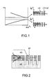
- the figure 1 illustrates the intensity of the electric field of an electromagnetic wave propagating in this type of structure and shows the dispersion diagram of a structure of period a in the first Brillouin zone; the wave vector k is in the range 0 ⁇ k ⁇ / a.
- artificially structure materials for example semiconductors, to take advantage of diffraction effects, thereby enabling the development of passive and active optical functions necessary, for example, for optical fiber telecommunications networks.
- one of the major attractions of these structures is based on the controlled insertion of defects within the crystal. These defects can generate states at bandgap frequencies of the crystal and thus allow a propagating electromagnetic field for these frequencies. A control of the propagation of light within the crystal and at the wavelength scale is then possible via these defects. The use of these structures thus opens the way to the miniaturization of components in integrated optics.
- a very thin layer is thus isolated, thus constituting a membrane that can typically have a thickness h of the order of 150 nanometers to 300 nanometers for applications targeting the spectral range between about 1 micron and 1.6 microns.
- h is between 0.1 and 0.3 times the wavelength.
- the material used can typically be silicon or a semiconductor material based on elements of columns III and V of the Mendeleyev periodic table ("III-V" semiconductors, for example GaAs, AlGaAs, GaInP, InP, AlGaAsP, .. .).
- Materials that can also be envisaged are the semiconductors of family II-VI (for example ZnO) as well as SiN.
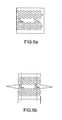
- a waveguide is created with a strong optical index variation as illustrated in FIG. figure 2 .
- the wave propagation speed and the dispersion of the guided modes can be adjusted by varying the size of the patterns.
- This silicon Si element is formed on the surface of an SiO 2 oxide layer and embedded in the polymer referenced Poly. It is thus possible to use it as an adapter.
- the Figures 3a and 3b illustrate this adapter element and the figure 4 represents the solution recommended in this article which consists in making a three-stage adaptation between the guided modes of the fibers F and those from the photonic crystal PhC.
- a first element A 1 couples the mode of the photonic crystal to that of a suspended ribbon guide. A transition is then made to a ribbon guide resting on the low index sacrificial layer. Finally, a last element A 2 adapts the optical mode of the latter to that of the optical fiber F.
- the adapter element on the surface of the SiO 2 layer is then in a heterogeneous environment. It rests on a substrate while its upper surface is not in contact with the same type of material. This property creates an asymmetry in the confinement of optical modes.
- the present invention proposes a mode adapter that transforms the mode of the photonic crystal into a propagative mode in Gaussian free space with a numerical aperture such that it allows efficient coupling with an optical fiber. through a standard adapted optics (micro-lens, lentil fiber, GRIN lens, micro-sphere).
- the subject of the invention is a photonic crystal circuit as defined in claim 1.
- the tip protrudes from the cleavage plane of the substrate in order to avoid parasitic reflections on the latter.
- the membrane is made of silicon.
- the membrane is of type III-V material such as GaAs, GaAlAs, GaInP, InP, GaInAsP.
- the thickness of the membrane is between about 100 nanometers and 300 nanometers for applications in the range of 900nm to 1600nm.
- the photonic crystal comprises units having a periodicity of the order of a few hundred nanometers.
- the photonic crystal patterns are holes having radii of the order of 120 to 130 nanometers depending on the target operating wavelength.
- the operation of producing a groove is carried out over a width of the order of a hundred nanometers.
- the invention further relates to an optical system comprising a photonic crystal circuit according to the invention, an adaptive optics and an optical fiber.
- the adaptive optics is of the micro-lens or GRIN type (graded index) type.
- a photonic crystal circuit capable of being coupled to a standard optical fiber and which minimizes losses during the transmission of photons from the optical crystal into the fiber.
- This circuit includes as illustrated in figure 5 , a membrane 11 made of a thin layer of semiconductor material within which are introduced periodic patterns that can typically be holes.
- a guide 12 is made at the level of this membrane and materialized by an absence of periodic patterns.
- This membrane is developed on the surface of a substrate 10a which may advantageously comprise a so-called sacrificial 10b on which are formed the periodic patterns Mi shaped holes formed within the membrane 11.
- the photon guide is extended by an adapter element 13 having a section gradient without periodic patterns so as to create a mode adaptation at the output of the guide.
- An additional advantage of the photonic crystal circuit of the present invention is the strong reduction of parasitic reflections at the input / output facets, eliminating the need for specific antireflection treatments which are required with abrupt fracture of the output of a photonic crystal circuit of the prior art.
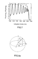
- the radiation patterns of these structures are illustrated in figure 8b and 8c and show a better directivity with adapter element.
- the dashed line curves 8b 1 and 8c 1 are relative to the sagittal plane, the curves in bold lines 8b 2 and 8c 2 are relative to the azimuthal plane in the polar coordinate coordinate system illustrated in FIG. figure 8a .
- the appearance of a quasi-circular mode reflects the improvement of the coupling in the case of the structure with tip ensuring the adaptation function.
- One of the major advantages of the present invention also lies in the simplicity of development of the tip termination guide which can be performed at the same time as the other technological steps that manufacture the photonic crystal circuit.
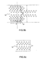
- a stack of a sacrificial layer 10b and a layer of semiconductor material 11 providing the membrane function, in which holes are made, are produced. locally Mi, while retaining a patternless area dedicated to the guide 12 as illustrated in figure 9a .
- the distance d represented on the figure 9b typically can be of the order of 10 .mu.m to 40 .mu.m; this value can be reduced according to the cleavage tolerances as well as the alignment accuracy of the patterns with respect to the crystalline plane of the semiconductor.
- cleavage step is used to isolate the tip at the edge of the guide as shown in FIG. Figure 9c .
- the photonic crystal circuit thus produced can advantageously be integrated into an optical system.
- the tip of said circuit is coupled to an optical fiber whose end may advantageously be provided with a lens that can typically have a focal length of the order of 10 to 20 microns.
- the figure 10 illustrates an example of application in which the photonic crystal equipped with its adapter portion provides the function of coupler is particularly interesting.
- couplers C 1 , C 2 and C 3 are used to couple the input signals Se and control Sc to guides arranged to achieve an interferometer architecture.
- the guides are made within photonic crystals of membrane type, by modification of the periodic structure, typically performed by lack of patterns.
- the device also includes photodetectors PD1 and PD2 for selecting signals resulting from interference of the input and control signals and for sampling the information carrying signal.
- the overall size of such a device can be extremely compact, the dimension d can be of the order of a few millimeters.
Landscapes
- Physics & Mathematics (AREA)
- Engineering & Computer Science (AREA)
- Optics & Photonics (AREA)
- General Physics & Mathematics (AREA)
- Microelectronics & Electronic Packaging (AREA)
- Chemical & Material Sciences (AREA)
- Nanotechnology (AREA)
- Crystallography & Structural Chemistry (AREA)
- Biophysics (AREA)
- Life Sciences & Earth Sciences (AREA)
- Power Engineering (AREA)
- Optical Integrated Circuits (AREA)
- Optical Couplings Of Light Guides (AREA)
Claims (10)
- Schaltung mit photonischem Kristall, die Folgendes umfasst: einen Leiter (12), der in einer Membran (11) aus photonischem Kristall auf der Oberfläche eines Substrats (10a) ausgebildet ist, und einen mit dem Leiter gekoppelten Modenadapter (13), dadurch gekennzeichnet, dass die Membran einen konstitutiven zentralen Punkt des Modenadapters mit einem Gradientenabschnitt als Abschluss des Leiters umfasst, wobei der Punkt so aufgehängt ist, der er die Mode des photonischen Kristalls in eine Ausbreitungsmode im freien Raum des Gauss'schen Typs konvertiert.
- Schaltung mit photonischem Kristall nach Anspruch 1, dadurch gekennzeichnet, dass die Membran aus Silicium besteht.
- Schaltung mit photonischem Kristall nach Anspruch 1, dadurch gekennzeichnet, dass die Membran aus einem Material des Typs III-V wie GaAs, GaAIAs, GaInP oder InP, GaInAsP besteht.
- Schaltung mit photonischem Kristall nach einem der Ansprüche 1 bis 3, dadurch gekennzeichnet, dass die Dicke der Membran zwischen etwa 100 Nanometer und 300 Nanometer liegt.
- Schaltung mit photonischem Kristall nach einem der Ansprüche 1 bis 4, dadurch gekennzeichnet, dass das photonische Kristall Muster mit einer Periodizität in der Größenordnung von mehreren hundert Nanometern hat.
- Schaltung mit photonischem Kristall nach einem der Ansprüche 1 bis 5, dadurch gekennzeichnet, dass die Muster des photonischen Kristalls Löcher mit Radien in der Größenordnung von 120 bis 130 Nanometer sind.
- Verfahren zur Herstellung einer Schaltung mit photonischem Kristall nach einem der Ansprüche 1 bis 6, dadurch gekennzeichnet, dass es die folgenden Schritte beinhaltet:- Erzeugen einer Nut auf der Oberfläche der Membran;- Durchführen eines Vorgangs zum Angreifen der Opferschicht (10b);- Durchführen eines Spaltvorgangs zum Trennen des konstitutiven Punkts des Adapters von der zuvor erzeugten Nut.
- Verfahren zur Herstellung einer photonischen Schaltung nach Anspruch 7, dadurch gekennzeichnet, dass der Vorgang zum Erzeugen einer Nut auf einer Breite in der Größenordnung von hundert Nanometern durchgeführt wird.
- Optisches System, umfassend eine photonische Schaltung nach einem der Ansprüche 1 bis 6, eine adaptive Optik und eine Faseroptik.
- Optisches System nach Anspruch 9, dadurch gekennzeichnet, dass die adaptive Optik vom Typ einer Mikrolinse oder einer GRIN-Linse ist.
Applications Claiming Priority (1)
| Application Number | Priority Date | Filing Date | Title |
|---|---|---|---|
| FR0803987A FR2933780B1 (fr) | 2008-07-11 | 2008-07-11 | Circuit a cristal photonique comportant un adaptateur de modes guides et systeme optique comportant ledit circuit couple avec une fibre optique |
Publications (2)
| Publication Number | Publication Date |
|---|---|
| EP2144098A1 EP2144098A1 (de) | 2010-01-13 |
| EP2144098B1 true EP2144098B1 (de) | 2011-10-12 |
Family
ID=40428320
Family Applications (1)
| Application Number | Title | Priority Date | Filing Date |
|---|---|---|---|
| EP09164816A Active EP2144098B1 (de) | 2008-07-11 | 2009-07-07 | Planarer Wellenleiter mit photonischem Kristall mit einem Modenkonverter und optisches System mit dem Wellenleiter gekoppelt mit einer optischer Faser |
Country Status (4)
| Country | Link |
|---|---|
| US (1) | US8019186B2 (de) |
| EP (1) | EP2144098B1 (de) |
| AT (1) | ATE528672T1 (de) |
| FR (1) | FR2933780B1 (de) |
Families Citing this family (2)
| Publication number | Priority date | Publication date | Assignee | Title |
|---|---|---|---|---|
| FR2933780B1 (fr) * | 2008-07-11 | 2010-12-17 | Thales Sa | Circuit a cristal photonique comportant un adaptateur de modes guides et systeme optique comportant ledit circuit couple avec une fibre optique |
| US10261250B2 (en) * | 2014-06-16 | 2019-04-16 | University Of Copenhagen | Efficient spin-photon interface using glide-plane-symmetric waveguide |
Family Cites Families (9)
| Publication number | Priority date | Publication date | Assignee | Title |
|---|---|---|---|---|
| US6711200B1 (en) * | 1999-09-07 | 2004-03-23 | California Institute Of Technology | Tuneable photonic crystal lasers and a method of fabricating the same |
| US7110628B2 (en) * | 2002-07-12 | 2006-09-19 | Massachusetts Institute Of Technology | Reconfigurable microphotonics devices via deformable membrane platforms |
| CN1761898A (zh) * | 2003-03-14 | 2006-04-19 | 日本电气株式会社 | 对光子晶体光导波路的光入射方法及其构造 |
| US7157296B2 (en) * | 2003-04-22 | 2007-01-02 | University Of Delaware | Etchless fabrication of planar photonic crystal structures in high refractive index material |
| US7206488B1 (en) * | 2004-09-22 | 2007-04-17 | The Board Of Trustees Of The Leland Stanford Junior University | Coupled photonic crystal resonator array arrangements and applications |
| US7289221B2 (en) * | 2004-09-27 | 2007-10-30 | Hewlett-Packard Development Company, L.P. | Mach Zehnder photonic crystal sensors and methods |
| FR2884916B1 (fr) * | 2005-04-25 | 2007-06-22 | Commissariat Energie Atomique | Detecteur optique ultrasensible a grande resolution temporelle, utilisant un plasmon de surface |
| US7894699B2 (en) * | 2006-10-16 | 2011-02-22 | Hewlett-Packard Development Company, L.P. | Photonic based interconnects for interconnecting multiple integrated circuits |
| FR2933780B1 (fr) * | 2008-07-11 | 2010-12-17 | Thales Sa | Circuit a cristal photonique comportant un adaptateur de modes guides et systeme optique comportant ledit circuit couple avec une fibre optique |
-
2008
- 2008-07-11 FR FR0803987A patent/FR2933780B1/fr active Active
-
2009
- 2009-07-07 EP EP09164816A patent/EP2144098B1/de active Active
- 2009-07-07 AT AT09164816T patent/ATE528672T1/de not_active IP Right Cessation
- 2009-07-08 US US12/499,727 patent/US8019186B2/en active Active
Also Published As
| Publication number | Publication date |
|---|---|
| EP2144098A1 (de) | 2010-01-13 |
| US20100272387A1 (en) | 2010-10-28 |
| FR2933780B1 (fr) | 2010-12-17 |
| ATE528672T1 (de) | 2011-10-15 |
| FR2933780A1 (fr) | 2010-01-15 |
| US8019186B2 (en) | 2011-09-13 |
Similar Documents
| Publication | Publication Date | Title |
|---|---|---|
| Chen et al. | Device engineering for silicon photonics | |
| FR3066615B1 (fr) | Puce photonique a structure de collimation integree | |
| EP2169436B1 (de) | Lichtkoppler zwischen einer Lichtleitfaser und einem Wellenleiter auf einem Substrat | |
| US9599781B1 (en) | Plasmon-assisted optical vias for photonic ASICS | |
| SG181649A1 (en) | Photonic integrated circuit having a waveguide-grating coupler | |
| EP3339924A1 (de) | Optimierter integrierter photonenschaltkreis | |
| EP0637764A1 (de) | Herstellung einer optischen Kopplungsstruktur, die einen abgespaltenen optischen Wellenleiter und eine Halterung für optische Fasern integriert | |
| Audet et al. | Surface-normal Ge/SiGe asymmetric Fabry–Perot optical modulators fabricated on silicon substrates | |
| US20230400652A1 (en) | Heteroepitaxially Integrated Compound Semiconductor Optical Devices with On-Chip Waveguides | |
| JP2017219562A (ja) | 光回路デバイスとこれを用いた光トランシーバ、及び光半導体素子 | |
| Viktorovitch et al. | 3D harnessing of light with 2.5 D photonic crystals | |
| WO2021178727A1 (en) | Evanescent coupler mode converters | |
| FR2933781A1 (fr) | Extracteur de photons a cristaux photoniques pour micro-sources optiques a fort rendement | |
| EP2144098A1 (de) | Planarer Wellenleiter mit photonischem Kristall mit einem Modenkonverter und optisches System mit dem Wellenleiter gekoppelt mit einer optischer Faser | |
| Van Thourhout et al. | Coupling mechanisms for a heterogeneous silicon nanowire platform | |
| EP2442164A1 (de) | Optischer Nanophotonen-Duplexer | |
| CN101387763A (zh) | 基于光子晶体结构的光信号延迟器件 | |
| Dupont et al. | Low-loss InGaAsP/InP submicron optical waveguides fabricated by ICP etching | |
| Bondarenko et al. | Extremely compact hybrid III-V/SOI lasers: design and fabrication approaches | |
| Jung et al. | High‐bandwidth InGaAs photodetectors heterogeneously integrated on silicon waveguides using optofluidic assembly | |
| Bazin | III-V Semiconductor Nanocavitieson Silicon-On-Insulator Waveguide: Laser Emission, Switching and Optical Memory | |
| EP4083671B1 (de) | Integrierter optischer wellenleiter | |
| Fulbert et al. | Photonics—Electronics integration on CMOS | |
| Rodriguez | Technology development of nano-scale photonic integrated circuits in III-V membranes | |
| Dezfuli | Second-Order Enhanced Coupling Strength Grating Out-Couplers for a Monolithic Laser-Electro-Absorption Modulator |
Legal Events
| Date | Code | Title | Description |
|---|---|---|---|
| PUAI | Public reference made under article 153(3) epc to a published international application that has entered the european phase |
Free format text: ORIGINAL CODE: 0009012 |
|
| AK | Designated contracting states |
Kind code of ref document: A1 Designated state(s): AT BE BG CH CY CZ DE DK EE ES FI FR GB GR HR HU IE IS IT LI LT LU LV MC MK MT NL NO PL PT RO SE SI SK SM TR |
|
| 17P | Request for examination filed |
Effective date: 20100507 |
|
| 17Q | First examination report despatched |
Effective date: 20100528 |
|
| GRAP | Despatch of communication of intention to grant a patent |
Free format text: ORIGINAL CODE: EPIDOSNIGR1 |
|
| RIC1 | Information provided on ipc code assigned before grant |
Ipc: G02B 6/13 20060101ALI20110510BHEP Ipc: G02B 6/122 20060101AFI20110510BHEP Ipc: G02B 6/30 20060101ALI20110510BHEP |
|
| GRAS | Grant fee paid |
Free format text: ORIGINAL CODE: EPIDOSNIGR3 |
|
| GRAA | (expected) grant |
Free format text: ORIGINAL CODE: 0009210 |
|
| AK | Designated contracting states |
Kind code of ref document: B1 Designated state(s): AT BE BG CH CY CZ DE DK EE ES FI FR GB GR HR HU IE IS IT LI LT LU LV MC MK MT NL NO PL PT RO SE SI SK SM TR |
|
| REG | Reference to a national code |
Ref country code: GB Ref legal event code: FG4D Free format text: NOT ENGLISH |
|
| REG | Reference to a national code |
Ref country code: CH Ref legal event code: EP |
|
| REG | Reference to a national code |
Ref country code: IE Ref legal event code: FG4D |
|
| REG | Reference to a national code |
Ref country code: DE Ref legal event code: R096 Ref document number: 602009003011 Country of ref document: DE Effective date: 20111229 |
|
| REG | Reference to a national code |
Ref country code: NL Ref legal event code: VDEP Effective date: 20111012 |
|
| LTIE | Lt: invalidation of european patent or patent extension |
Effective date: 20111012 |
|
| REG | Reference to a national code |
Ref country code: AT Ref legal event code: MK05 Ref document number: 528672 Country of ref document: AT Kind code of ref document: T Effective date: 20111012 |
|
| PG25 | Lapsed in a contracting state [announced via postgrant information from national office to epo] |
Ref country code: LT Free format text: LAPSE BECAUSE OF FAILURE TO SUBMIT A TRANSLATION OF THE DESCRIPTION OR TO PAY THE FEE WITHIN THE PRESCRIBED TIME-LIMIT Effective date: 20111012 Ref country code: NO Free format text: LAPSE BECAUSE OF FAILURE TO SUBMIT A TRANSLATION OF THE DESCRIPTION OR TO PAY THE FEE WITHIN THE PRESCRIBED TIME-LIMIT Effective date: 20120112 Ref country code: IS Free format text: LAPSE BECAUSE OF FAILURE TO SUBMIT A TRANSLATION OF THE DESCRIPTION OR TO PAY THE FEE WITHIN THE PRESCRIBED TIME-LIMIT Effective date: 20120212 |
|
| REG | Reference to a national code |
Ref country code: IE Ref legal event code: FD4D |
|
| PG25 | Lapsed in a contracting state [announced via postgrant information from national office to epo] |
Ref country code: GR Free format text: LAPSE BECAUSE OF FAILURE TO SUBMIT A TRANSLATION OF THE DESCRIPTION OR TO PAY THE FEE WITHIN THE PRESCRIBED TIME-LIMIT Effective date: 20120113 Ref country code: HR Free format text: LAPSE BECAUSE OF FAILURE TO SUBMIT A TRANSLATION OF THE DESCRIPTION OR TO PAY THE FEE WITHIN THE PRESCRIBED TIME-LIMIT Effective date: 20111012 Ref country code: LV Free format text: LAPSE BECAUSE OF FAILURE TO SUBMIT A TRANSLATION OF THE DESCRIPTION OR TO PAY THE FEE WITHIN THE PRESCRIBED TIME-LIMIT Effective date: 20111012 Ref country code: NL Free format text: LAPSE BECAUSE OF FAILURE TO SUBMIT A TRANSLATION OF THE DESCRIPTION OR TO PAY THE FEE WITHIN THE PRESCRIBED TIME-LIMIT Effective date: 20111012 Ref country code: PT Free format text: LAPSE BECAUSE OF FAILURE TO SUBMIT A TRANSLATION OF THE DESCRIPTION OR TO PAY THE FEE WITHIN THE PRESCRIBED TIME-LIMIT Effective date: 20120213 Ref country code: SI Free format text: LAPSE BECAUSE OF FAILURE TO SUBMIT A TRANSLATION OF THE DESCRIPTION OR TO PAY THE FEE WITHIN THE PRESCRIBED TIME-LIMIT Effective date: 20111012 Ref country code: SE Free format text: LAPSE BECAUSE OF FAILURE TO SUBMIT A TRANSLATION OF THE DESCRIPTION OR TO PAY THE FEE WITHIN THE PRESCRIBED TIME-LIMIT Effective date: 20111012 |
|
| PG25 | Lapsed in a contracting state [announced via postgrant information from national office to epo] |
Ref country code: CY Free format text: LAPSE BECAUSE OF FAILURE TO SUBMIT A TRANSLATION OF THE DESCRIPTION OR TO PAY THE FEE WITHIN THE PRESCRIBED TIME-LIMIT Effective date: 20111012 |
|
| PG25 | Lapsed in a contracting state [announced via postgrant information from national office to epo] |
Ref country code: BG Free format text: LAPSE BECAUSE OF FAILURE TO SUBMIT A TRANSLATION OF THE DESCRIPTION OR TO PAY THE FEE WITHIN THE PRESCRIBED TIME-LIMIT Effective date: 20120112 Ref country code: EE Free format text: LAPSE BECAUSE OF FAILURE TO SUBMIT A TRANSLATION OF THE DESCRIPTION OR TO PAY THE FEE WITHIN THE PRESCRIBED TIME-LIMIT Effective date: 20111012 Ref country code: CZ Free format text: LAPSE BECAUSE OF FAILURE TO SUBMIT A TRANSLATION OF THE DESCRIPTION OR TO PAY THE FEE WITHIN THE PRESCRIBED TIME-LIMIT Effective date: 20111012 Ref country code: SK Free format text: LAPSE BECAUSE OF FAILURE TO SUBMIT A TRANSLATION OF THE DESCRIPTION OR TO PAY THE FEE WITHIN THE PRESCRIBED TIME-LIMIT Effective date: 20111012 Ref country code: IE Free format text: LAPSE BECAUSE OF FAILURE TO SUBMIT A TRANSLATION OF THE DESCRIPTION OR TO PAY THE FEE WITHIN THE PRESCRIBED TIME-LIMIT Effective date: 20111012 Ref country code: DK Free format text: LAPSE BECAUSE OF FAILURE TO SUBMIT A TRANSLATION OF THE DESCRIPTION OR TO PAY THE FEE WITHIN THE PRESCRIBED TIME-LIMIT Effective date: 20111012 |
|
| PLBE | No opposition filed within time limit |
Free format text: ORIGINAL CODE: 0009261 |
|
| STAA | Information on the status of an ep patent application or granted ep patent |
Free format text: STATUS: NO OPPOSITION FILED WITHIN TIME LIMIT |
|
| PG25 | Lapsed in a contracting state [announced via postgrant information from national office to epo] |
Ref country code: IT Free format text: LAPSE BECAUSE OF FAILURE TO SUBMIT A TRANSLATION OF THE DESCRIPTION OR TO PAY THE FEE WITHIN THE PRESCRIBED TIME-LIMIT Effective date: 20111012 Ref country code: PL Free format text: LAPSE BECAUSE OF FAILURE TO SUBMIT A TRANSLATION OF THE DESCRIPTION OR TO PAY THE FEE WITHIN THE PRESCRIBED TIME-LIMIT Effective date: 20111012 Ref country code: RO Free format text: LAPSE BECAUSE OF FAILURE TO SUBMIT A TRANSLATION OF THE DESCRIPTION OR TO PAY THE FEE WITHIN THE PRESCRIBED TIME-LIMIT Effective date: 20111012 |
|
| 26N | No opposition filed |
Effective date: 20120713 |
|
| REG | Reference to a national code |
Ref country code: DE Ref legal event code: R097 Ref document number: 602009003011 Country of ref document: DE Effective date: 20120713 |
|
| BERE | Be: lapsed |
Owner name: THALES Effective date: 20120731 |
|
| PG25 | Lapsed in a contracting state [announced via postgrant information from national office to epo] |
Ref country code: AT Free format text: LAPSE BECAUSE OF FAILURE TO SUBMIT A TRANSLATION OF THE DESCRIPTION OR TO PAY THE FEE WITHIN THE PRESCRIBED TIME-LIMIT Effective date: 20111012 |
|
| PG25 | Lapsed in a contracting state [announced via postgrant information from national office to epo] |
Ref country code: MK Free format text: LAPSE BECAUSE OF FAILURE TO SUBMIT A TRANSLATION OF THE DESCRIPTION OR TO PAY THE FEE WITHIN THE PRESCRIBED TIME-LIMIT Effective date: 20111012 Ref country code: MC Free format text: LAPSE BECAUSE OF NON-PAYMENT OF DUE FEES Effective date: 20120731 |
|
| PG25 | Lapsed in a contracting state [announced via postgrant information from national office to epo] |
Ref country code: BE Free format text: LAPSE BECAUSE OF NON-PAYMENT OF DUE FEES Effective date: 20120731 |
|
| PG25 | Lapsed in a contracting state [announced via postgrant information from national office to epo] |
Ref country code: FI Free format text: LAPSE BECAUSE OF FAILURE TO SUBMIT A TRANSLATION OF THE DESCRIPTION OR TO PAY THE FEE WITHIN THE PRESCRIBED TIME-LIMIT Effective date: 20111012 |
|
| PG25 | Lapsed in a contracting state [announced via postgrant information from national office to epo] |
Ref country code: MT Free format text: LAPSE BECAUSE OF FAILURE TO SUBMIT A TRANSLATION OF THE DESCRIPTION OR TO PAY THE FEE WITHIN THE PRESCRIBED TIME-LIMIT Effective date: 20111012 |
|
| PG25 | Lapsed in a contracting state [announced via postgrant information from national office to epo] |
Ref country code: ES Free format text: LAPSE BECAUSE OF FAILURE TO SUBMIT A TRANSLATION OF THE DESCRIPTION OR TO PAY THE FEE WITHIN THE PRESCRIBED TIME-LIMIT Effective date: 20120123 |
|
| REG | Reference to a national code |
Ref country code: CH Ref legal event code: PL |
|
| PG25 | Lapsed in a contracting state [announced via postgrant information from national office to epo] |
Ref country code: LI Free format text: LAPSE BECAUSE OF NON-PAYMENT OF DUE FEES Effective date: 20130731 Ref country code: CH Free format text: LAPSE BECAUSE OF NON-PAYMENT OF DUE FEES Effective date: 20130731 Ref country code: TR Free format text: LAPSE BECAUSE OF FAILURE TO SUBMIT A TRANSLATION OF THE DESCRIPTION OR TO PAY THE FEE WITHIN THE PRESCRIBED TIME-LIMIT Effective date: 20111012 |
|
| PG25 | Lapsed in a contracting state [announced via postgrant information from national office to epo] |
Ref country code: SM Free format text: LAPSE BECAUSE OF FAILURE TO SUBMIT A TRANSLATION OF THE DESCRIPTION OR TO PAY THE FEE WITHIN THE PRESCRIBED TIME-LIMIT Effective date: 20111012 Ref country code: LU Free format text: LAPSE BECAUSE OF NON-PAYMENT OF DUE FEES Effective date: 20120707 |
|
| PG25 | Lapsed in a contracting state [announced via postgrant information from national office to epo] |
Ref country code: HU Free format text: LAPSE BECAUSE OF FAILURE TO SUBMIT A TRANSLATION OF THE DESCRIPTION OR TO PAY THE FEE WITHIN THE PRESCRIBED TIME-LIMIT Effective date: 20090707 |
|
| REG | Reference to a national code |
Ref country code: FR Ref legal event code: PLFP Year of fee payment: 8 |
|
| REG | Reference to a national code |
Ref country code: FR Ref legal event code: PLFP Year of fee payment: 9 |
|
| REG | Reference to a national code |
Ref country code: FR Ref legal event code: PLFP Year of fee payment: 10 |
|
| PGFP | Annual fee paid to national office [announced via postgrant information from national office to epo] |
Ref country code: GB Payment date: 20250619 Year of fee payment: 17 |
|
| PGFP | Annual fee paid to national office [announced via postgrant information from national office to epo] |
Ref country code: FR Payment date: 20250623 Year of fee payment: 17 |
|
| PGFP | Annual fee paid to national office [announced via postgrant information from national office to epo] |
Ref country code: DE Payment date: 20250618 Year of fee payment: 17 |