EP2141812A1 - Relaying circuit, information processing device, and relaying method - Google Patents
Relaying circuit, information processing device, and relaying method Download PDFInfo
- Publication number
- EP2141812A1 EP2141812A1 EP07742021A EP07742021A EP2141812A1 EP 2141812 A1 EP2141812 A1 EP 2141812A1 EP 07742021 A EP07742021 A EP 07742021A EP 07742021 A EP07742021 A EP 07742021A EP 2141812 A1 EP2141812 A1 EP 2141812A1
- Authority
- EP
- European Patent Office
- Prior art keywords
- voltage
- circuit
- buffer
- tri
- state buffer
- Prior art date
- Legal status (The legal status is an assumption and is not a legal conclusion. Google has not performed a legal analysis and makes no representation as to the accuracy of the status listed.)
- Withdrawn
Links
Images






Classifications
-
- H—ELECTRICITY
- H03—ELECTRONIC CIRCUITRY
- H03K—PULSE TECHNIQUE
- H03K19/00—Logic circuits, i.e. having at least two inputs acting on one output; Inverting circuits
- H03K19/0175—Coupling arrangements; Interface arrangements
- H03K19/017509—Interface arrangements
-
- H—ELECTRICITY
- H03—ELECTRONIC CIRCUITRY
- H03K—PULSE TECHNIQUE
- H03K19/00—Logic circuits, i.e. having at least two inputs acting on one output; Inverting circuits
- H03K19/003—Modifications for increasing the reliability for protection
- H03K19/00346—Modifications for eliminating interference or parasitic voltages or currents
Definitions
- the present invention relates to a relay circuit, an information processing apparatus, and a relay method that relay signal transmission between circuits.
- a bidirectional buffer is sometimes interposed between the devices in order to prevent breakdown of the devices.
- either one of the two power supplies can be connected to the enable terminal of the bidirectional buffer (also referred to as "transceiver") to protect the device of the system that is powered off.
- FIG. 10 is a block diagram illustrating an example of the configuration of a conventional first information processing apparatus.
- the information processing apparatus includes a power supply 11 (first voltage generating circuit), a DC-DC converter 12 (second voltage generating circuit), a system control system controller 13 (first circuit), an ASIC (Application Specific Integrated Circuit) 14 (second circuit), and a bidirectional buffer 15 (buffer circuit).
- the system control system controller 13 has I2CBUS_A which is composed of an I2C (I Square C) BUS, a two-wire bidirectional interface for external communication.
- the ASIC 14 has 12CBUS_B which is composed of an 12C BUS for external communication.
- FIG. 11 is a circuit diagram illustrating an example of the configuration of the bidirectional buffer.
- the bidirectional buffer 15 relays communication between the 12CBUS_A of the system control system controller 13 and the 12CBUS_B of the ASIC 14.
- the bidirectional buffer 15 is composed of tri-state buffers 21 a and 21 b.
- the tri-state buffers 21 a and 21 b are powered by VCC1.
- VCC2 is input to the enable terminal of each of the tri-state buffers 21 a and 21 b.
- VCC2 input to the enable terminal exceeds a predetermined threshold and becomes H (High)
- the signal input from the I2CBUS_A is output to the I2CBUS_B
- the signal input from the I2CBUS_B is output to the I2CBUS_A.
- VCC2 input to the enable terminal falls below a predetermined threshold and becomes L (Low)
- the I2CBUS_A and the I2CBUS_B are cut off. It should be appreciated that the enable terminal of the tri-state buffer 21 b may be supplied with inverted VCC2.
- FIG. 12 is a timing chart illustrating the operation of the conventional first information processing apparatus.
- the timing chart depicts, from the top, the waveforms of AC power, a primary DC voltage, VCC1, a power-on instruction, and VCC2.
- the power supply 11 supplies the resident power source VCC1 to the system control system controller 13 and supplies the primary DC voltage to the DC-DC converter 12.
- the system control system controller 13 which is activated by VCC1 sends a power-on instruction to the DC-DC converter 12.
- the DC-DC converter 12 supplies VCC2 to the ASIC 14 and supplies VCC2 to the enable terminal (ENABLE) of the bidirectional buffer 15.
- VCC2 rises and falls gentler than the changes of the signals.
- FIG. 13 is a block diagram illustrating an example of the configuration of a conventional second information processing apparatus.
- the diagram includes a transmitting unit 23 (first circuit) instead of the system control system controller 13, a receiving unit 24 (second circuit) instead of the ASIC 14, and a unidirectional buffer 25 (buffer circuit: also referred to as "driver") instead of the bidirectional buffer 15.
- the transmitting unit 23 has a terminal of a signal SIGNAL-A to be transmitted outside.
- the receiving unit 24 has a terminal of a signal SIGNAL_B to be received from outside.
- FIG. 14 is a block diagram illustrating an example of the configuration of the unidirectional buffer.
- the unidirectional buffer 25 relays between SIGNAL_A and SIGNAL_B.
- the unidirectional buffer 25 is composed of a tri-state buffer 21 c which is controlled through the enable terminal.
- the tri-state buffer 21 c is powered by VCC1.
- VCC2 is supplied to the enable terminal of the tri-state buffer 21 c.
- the operation of the second information processing apparatus is the same as in FIG. 12 .
- the power supply 11 supplies the resident power source VCC1 to the transmitting unit 23 and supplies the primary DC voltage to the DC-DC converter 12.
- the transmission unit 23 which is activated by VCC1 sends a power-on instruction to the DC-DC converter 12.
- the DC-DC converter 12 supplies VCC2 to the receiving unit 24 and inputs VCC2 to the enable terminal (ENABLE) of the unidirectional buffer 25.
- VCC2 input to the enable terminal exceeds a predetermined threshold and becomes H
- the signal input from SIGNAL_A is output to SIGNAL_B.
- VCC2 input to the enable terminal falls below a predetermined threshold and becomes L
- the signal input from SIGNAL_A is not output to SIGNAL_B but interrupted.
- Patent Document 1 Japanese Laid-Open Patent Publication No. 2000-151383
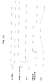
- FIG. 15 is a timing chart illustrating an example of the operation of the conventional bidirectional buffer.
- the timing chart illustrates the operation of the bidirectional buffer in the operation of the first information processing apparatus illustrated in FIG. 12 , depicting the waveforms of VCC1, VCC2, ENABLE, I2CBUS_B, and I2CBUS_A from the top.
- the connection described above makes VCC2 and ENABLE equal to each other.
- VCC1 from the power supply 11 rises initially, and then ENABLE rises along with the rise of VCC2 from the DC-DC converter 12.
- I2CBUS_A and 12CBUS_B become operable.
- ENABLE gradually falls with VCC2. Since the intermediate potential state of VCC2 and ENABLE lasts long, noise occurs in I2CBUS_A in the intermediate potential state.
- FIG. 16 is a timing chart illustrating an example of the operation of the conventional unidirectional buffer.
- the timing chart illustrates the operation of the unidirectional buffer for the same operation of the second information processing apparatus as that of the first information processing apparatus illustrated in FIG. 12 , depicting the waveforms of VCC1, VCC2, ENABLE, SIGNAL_A, and SIGNAL_B from the top.
- VCC1 from the power supply 11 rises initially, and then ENABLE rises along with the rise of VCC2 from the DC-DC converter 12.
- SIGNAL_A and SIGNAL_B become operable.
- ENABLE gradually falls with VCC2. Since the intermediate potential state of VCC2 and ENABLE lasts long, noise occurs in SIGNAL_B in the intermediate potential state.
- the present invention has been achieved in order to solve the foregoing problems, and it is an object of the present invention to provide a relay circuit, an information processing apparatus, and a relay method that prevents the occurrence of noise that results when the enable terminal of a buffer for relaying between circuits enters an intermediate potential state.
- the present invention is A relay circuit for relaying signal transmission between a first circuit that is driven by a first voltage and a second circuit that is driven by a second voltage different from the first voltage, the relay circuit being arranged between the first circuit and the second circuit, the relay circuit including: a waveform shaping circuit that obtains a shaped voltage by shaping a waveform of the second voltage in order to make a change of the second voltage steeper; and a buffer circuit that is driven by the first voltage and interrupts a signal transmission by the buffer circuit if the shaped voltage obtained by the waveform shaping circuit falls to or below a predetermined value, the shaped voltage being input to the buffer circuit as a control signal.
- the present invention also includes: a first voltage generating circuit that generates a first voltage; a second voltage generating circuit that generates a second voltage different from the first voltage; a first circuit that is driven by the first voltage; a second circuit that is driven by the second voltage; a waveform shaping circuit that obtains a shaped voltage by shaping a waveform of the second voltage in order to make a change of the second voltage steeper; and a buffer circuit that is arranged between the first circuit and the second circuit, is driven by the first voltage and interrupts a signal transmission by the buffer circuit if the shaped voltage obtained by the waveform shaping circuit falls to or below a predetermined value, the shaped voltage being input to the buffer circuit as a control signal.
- the present invention also is a relay method for relaying signal transmission between a first circuit that is driven by a first voltage and a second circuit that is driven by a second voltage different from the first voltage, the method including: a waveform shaping step that obtains a shaped voltage by shaping a waveform of the second voltage in order to make a change of the second voltage steeper; and an interruption step that interrupts a signal transmission by a buffer circuit if the shaped voltage obtained by the waveform shaping circuit falls to or below a predetermined value, the buffer circuit being arranged between the first circuit and the second circuit, the buffer circuit being driven by the first voltage, the shaped voltage being input to the buffer circuit as a control signal.
- the present embodiment will deal with a relay circuit and an information processing apparatus that use a bidirectional buffer.
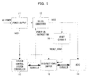
- FIG. 1 is a block diagram illustrating an example of the configuration of the information processing apparatus according to the present embodiment.
- the diagram as compared to FIG. 10 , newly includes a reset circuit 16 (waveform shaping circuit).
- the reset circuit 16 generates -RESET_VCC2 from VCC2 which is supplied from a DC-DC converter 12, and outputs -RESET_VCC2 to the enable terminal (ENABLE) of a bidirectional buffer 15 (waveform shaping step).
- -RESET_VCC2 is a signal that changes steeply with VCC2.
- -RESET_VCC2 can be used in other devices in the information processing apparatus as a power-on reset signal, a reset signal that is linked with power-on.
- the reset circuit 16 thus yields no increase in the cost of the information processing apparatus.
- the relay circuit corresponds to the reset circuit 16 and the bidirectional buffer 15 according to the present embodiment.
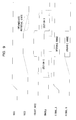
- FIG. 2 is a timing chart illustrating an example of the operation of the bidirectional buffer according to the present embodiment.
- the timing chart illustrates the operation of the bidirectional buffer for the same operation of the information processing apparatus as in FIG. 12 , depicting the waveforms of VCC1, VCC2, -RESET_VCC2, ENABLE, I2CBUS_B, and I2CBUS_A from the top.
- the operation of VCC1 and VCC2 is the same as in FIG. 12 .
- the connection described above makes -RESET_VCC2 and ENABLE equal to each other.
- the ENABLE waveform of the chart differs from that of FIG. 15 in section A where VCC2 rises and section B where VCC2 falls.
- the section A of the ENABLE waveform is steeper than the rise of VCC2.
- the section B of the ENABLE waveform is steeper than the fall of VCC2. Consequently, there occurs no intermediate potential state in the section B of the ENABLE waveform.
- ENABLE With VCC2 in the intermediate potential state, ENABLE becomes L and the bidirectional buffer 15 interrupts the signal transmission between I2CBUS_A and I2CBUS_B (interruption step), which can prevent the conventional production of noise in I2CBUS_A.
- the section A and section B of the ENABLE waveform are ascribable to the operation of the reset circuit 16.
- FIG. 3 is a block diagram illustrating an example of the configuration of the reset circuit according to the present embodiment.
- the reset circuit 16 includes a current source, a voltage source Vref, a comparator, a Schmitt trigger, a transistor A (Tr.A), a transistor B (Tr.B), an output transistor Pch (Tr.P), an output transistor Nch (Tr.N), an output capacitor, and resistors Ra, Rb, and Rc.
- FIG. 4 is a timing chart illustrating an example of the operation of the reset circuit according to the present embodiment.
- the upper section illustrates the waveform of VCC2 which is the input voltage to the reset circuit 16, and illustrates the waveform of -RESET_VCC2 which is the output voltage from the reset circuit 16.
- a release voltage is higher than a detection voltage, and the difference between the release voltage and the detection voltage is a hysteresis width.
- the minimum operating voltage is a minimum voltage at which each transistor operates.
- the operating states S1, S2, S3, S4, and S5 are defined according to the changes of VCC2.
- VCC2 decreases from a prescribed value to GND (ground voltage) and then increases from GND to the prescribed value.
- GND ground voltage
- S2 the state where VCC2 decreases from the prescribed voltage to the detection voltage
- S3 the state where VCC2 decreases from the minimum operating voltage to GND and increases from GND to the minimum operating voltage
- S4 the state where VCC2 increases from the minimum operating voltage to the detection voltage
- the state where VCC2 increases from the detection voltage to the prescribed voltage will be S5.
- the time at which decreasing VCC2 reaches the detection voltage will be Ta, and the time at which increasing VCC2 reaches the release voltage will be Tb. Because of the hysteresis mentioned above, there is a delay time between the transition from the state S4 to the state S5 and the time Tb.
- FIG. 5 is a table illustrating an example of the operating states of the reset circuit according to the present embodiment.
- the comparator (-) terminal input voltage, the comparator output, the states of Tr.A and Tr.B, the state of Tr.N, and the state of Tr.P are illustrated for each of the operating states S1, S2, S3, S4, and S5.
- Va of the comparator (-) terminal input voltage is expressed by the following equation:
- Vb of the comparator (-) terminal input voltage is expressed by the following equation:
- Vb Rb Ra + Rb ⁇ VCC ⁇ 2
- -RESET_VCC2 becomes equal to VCC2.
- VCC2 decreases to the detection voltage (Ta) so that Vref ⁇ Va.
- the comparator output is inverted from L to H, and -RESET_VCC2 is at GND.
- the states of Tr.N and Tr.P are undefined.
- -RESET_VCC2 is at GND.
- VCC2 increases to the release voltage (Tb) so that Ref ⁇ Vb.
- the comparator output reaches a threshold voltage for H, the Schmitt trigger output is inverted from H to L, and -RESET_VCC2 becomes equal to VCC2.
- FIG. 6 is a timing chart illustrating an example of the section A of the ENABLE waveform according to the present embodiment.
- the section A corresponds to the states S3, S4, and S5.
- ENABLE is in the L state.
- -RESET_VCC2 is equal to VCC2 until the power-on instruction becomes H and VCC2 increases from GND to the minimum operating voltage (for example, 0.8 V or so) (state S3).
- -RESET_VCC2 becomes equal to GND until VCC2 further increases to reach the release voltage (for example, 2.35 V or so) (state S4).
- VCC2 increases further, -RESET_VCC2 becomes equals to VCC2 and ENABLE enters the H state. Subsequently, VCC2 and -RESET_VCC2 reach the prescribed voltage (for example, 3.3 V) (state S5).
- FIG. 7 is a timing chart illustrating an example of the section B of the ENABLE waveform according to the present embodiment.
- the section B corresponds to the states S1, S2, and S3.
- ENABLE is in the H state.
- -RESET_VCC2 is equal to VCC2 until the power-on instruction becomes L and VCC2 decreases from the prescribed voltage to the detection voltage (for example, 2.25 V or so) (state S1).
- -RESET_VCC2 becomes equal to GND and ENABLE enters the L state until VCC2 further decreases to the minimum operating voltage (state S2).
- VCC2 decreases further, and -RESET-VCC2 becomes equal to VCC2.
- VCC2 and -RESET_VCC2 subsequently come to GND (state S3).
- the foregoing operation of the reset circuit 16 can make the section A of the ENABLE waveform steeper than the rise of VCC2, and make the section B of the ENABLE waveform steeper than the fall of VCC2. Consequently, ENABLE can be set to L during the period where VCC2 is in the intermediate potential state.
- the present embodiment will deal with a relay circuit and an information processing apparatus that use a unidirectional buffer.
- FIG. 8 is a block diagram illustrating an example of the configuration of the information processing apparatus according to the present embodiment.
- the same reference symbols as in FIG. 13 will designate components identical or equivalent to those illustrated in FIG. 13 , and description thereof will be omitted.
- the diagram newly includes a reset circuit 16.
- the reset circuit 16 generates -RESET_VCC2 from VCC2 which is supplied from the DC-DC converter 12, and outputs -RESET_VCC2 to the enable terminal (ENABLE) of the unidirectional buffer 25.
- the relay circuit corresponds to the reset circuit 16 and the unidirectional buffer 25 according to the present embodiment.
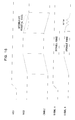
- FIG. 9 is a timing chart illustrating an example of the operation of the unidirectional buffer according to the present embodiment.
- the timing chart illustrates the operation of the unidirectional buffer 25 for the same operation of the information processing apparatus as in FIG. 12 , depicting the waveforms of VCC1, VCC2, -RESET_VCC2, ENABLE, and SIGNAL_B from the top.
- the operation of VCC1 and VCC2 is the same as in FIG. 12 .
- the ENABLE waveform of the chart differs from that of FIG. 16 in section C where VCC2 rises and section D where VCC2 falls.
- the section C of the ENABLE waveform is steeper than the rise of VCC2.
- the section D of the ENABLE waveform is steeper than the fall of VCC2. Consequently, there occurs no intermediate potential state in the section D of the ENABLE waveform.
- ENABLE With VCC2 in the intermediate potential state, ENABLE becomes L and the unidirectional buffer 25 interrupts the signal transmission from SIGNAL_A to SIGNAL_B (interruption step), which can prevent the conventional production of noise in SIGNAL_B.
- the section C and section D of the ENABLE waveform are ascribable to the operation of the reset circuit 16.
- Examples of the information processing apparatus may include a PC (Personal Computer) and a server.
- PC Personal Computer
Landscapes
- Engineering & Computer Science (AREA)
- Computer Hardware Design (AREA)
- Physics & Mathematics (AREA)
- Computing Systems (AREA)
- General Engineering & Computer Science (AREA)
- Mathematical Physics (AREA)
- Logic Circuits (AREA)
- Electronic Switches (AREA)
- Dc Digital Transmission (AREA)
Abstract
Description
- The present invention relates to a relay circuit, an information processing apparatus, and a relay method that relay signal transmission between circuits.
- When performing signal transmission between two devices that are driven by respective different power supplies, a bidirectional buffer is sometimes interposed between the devices in order to prevent breakdown of the devices. According to such a method, either one of the two power supplies can be connected to the enable terminal of the bidirectional buffer (also referred to as "transceiver") to protect the device of the system that is powered off.
-
FIG. 10 is a block diagram illustrating an example of the configuration of a conventional first information processing apparatus. The information processing apparatus includes a power supply 11 (first voltage generating circuit), a DC-DC converter 12 (second voltage generating circuit), a system control system controller 13 (first circuit), an ASIC (Application Specific Integrated Circuit) 14 (second circuit), and a bidirectional buffer 15 (buffer circuit). - The system
control system controller 13 has I2CBUS_A which is composed of an I2C (I Square C) BUS, a two-wire bidirectional interface for external communication. Similarly, the ASIC 14 has 12CBUS_B which is composed of an 12C BUS for external communication. -
FIG. 11 is a circuit diagram illustrating an example of the configuration of the bidirectional buffer. Thebidirectional buffer 15 relays communication between the 12CBUS_A of the systemcontrol system controller 13 and the 12CBUS_B of theASIC 14. Thebidirectional buffer 15 is composed of tri-statebuffers buffers buffers - When VCC2 input to the enable terminal exceeds a predetermined threshold and becomes H (High), the signal input from the I2CBUS_A is output to the I2CBUS_B and the signal input from the I2CBUS_B is output to the I2CBUS_A. When VCC2 input to the enable terminal falls below a predetermined threshold and becomes L (Low), the I2CBUS_A and the I2CBUS_B are cut off. It should be appreciated that the enable terminal of the tri-state
buffer 21 b may be supplied with inverted VCC2. -
FIG. 12 is a timing chart illustrating the operation of the conventional first information processing apparatus. The timing chart depicts, from the top, the waveforms of AC power, a primary DC voltage, VCC1, a power-on instruction, and VCC2. Initially, when the AC power is input to thepower supply 11 and a power breaker is tumed on, thepower supply 11 supplies the resident power source VCC1 to the systemcontrol system controller 13 and supplies the primary DC voltage to the DC-DC converter 12. - Next, the system
control system controller 13 which is activated by VCC1 sends a power-on instruction to the DC-DC converter 12. Receiving the power-on instruction, the DC-DC converter 12 supplies VCC2 to theASIC 14 and supplies VCC2 to the enable terminal (ENABLE) of thebidirectional buffer 15. Here, VCC2 rises and falls gentler than the changes of the signals. - Next, description will be given of the case where unidirectional communication is made from one device to another.
-
FIG. 13 is a block diagram illustrating an example of the configuration of a conventional second information processing apparatus. In the diagram, the same reference symbols as inFIG. 10 will designate components identical or equivalent to those illustrated inFIG. 1 , and description thereof will be omitted. The diagram, as compared toFIG. 1 , includes a transmitting unit 23 (first circuit) instead of the systemcontrol system controller 13, a receiving unit 24 (second circuit) instead of theASIC 14, and a unidirectional buffer 25 (buffer circuit: also referred to as "driver") instead of thebidirectional buffer 15. The transmittingunit 23 has a terminal of a signal SIGNAL-A to be transmitted outside. Thereceiving unit 24 has a terminal of a signal SIGNAL_B to be received from outside. -
FIG. 14 is a block diagram illustrating an example of the configuration of the unidirectional buffer. Theunidirectional buffer 25 relays between SIGNAL_A and SIGNAL_B. Theunidirectional buffer 25 is composed of a tri-statebuffer 21 c which is controlled through the enable terminal. The tri-statebuffer 21 c is powered by VCC1. VCC2 is supplied to the enable terminal of the tri-statebuffer 21 c. - The operation of the second information processing apparatus is the same as in
FIG. 12 . Initially, when the AC power is input to thepower supply 11 and the power breaker is tumed on, thepower supply 11 supplies the resident power source VCC1 to the transmittingunit 23 and supplies the primary DC voltage to the DC-DC converter 12. - Next, the
transmission unit 23 which is activated by VCC1 sends a power-on instruction to the DC-DC converter 12. Receiving the power-on instruction, the DC-DC converter 12 supplies VCC2 to the receivingunit 24 and inputs VCC2 to the enable terminal (ENABLE) of theunidirectional buffer 25. - When VCC2 input to the enable terminal exceeds a predetermined threshold and becomes H, the signal input from SIGNAL_A is output to SIGNAL_B. When VCC2 input to the enable terminal falls below a predetermined threshold and becomes L, the signal input from SIGNAL_A is not output to SIGNAL_B but interrupted.
- Among conventional technologies pertaining to the present invention is an output buffer circuit that prevents the occurrence of a leak current and can output a voltage up to an applied voltage quickly when a voltage higher than its own power supply voltage is applied to a common bus (for example, see patent document 1). Patent Document 1: Japanese Laid-Open Patent Publication No.
2000-151383 - Now, when the power supply connected to the enable terminal of the bidirectional buffer is tumed off, the voltage of the power supply falls slowly due to load capacitances, so that the intermediate potential state can sometimes last long. In such cases, noise occurs at the input and output ends of the bidirectional buffer, sometimes causing system malfunction.
-
FIG. 15 is a timing chart illustrating an example of the operation of the conventional bidirectional buffer. The timing chart illustrates the operation of the bidirectional buffer in the operation of the first information processing apparatus illustrated inFIG. 12 , depicting the waveforms of VCC1, VCC2, ENABLE, I2CBUS_B, and I2CBUS_A from the top. The connection described above makes VCC2 and ENABLE equal to each other. VCC1 from thepower supply 11 rises initially, and then ENABLE rises along with the rise of VCC2 from the DC-DC converter 12. - When VCC2 and ENABLE reach a prescribed voltage, I2CBUS_A and 12CBUS_B become operable. Next, when the DC-
DC converter 12 is powered off, ENABLE gradually falls with VCC2. Since the intermediate potential state of VCC2 and ENABLE lasts long, noise occurs in I2CBUS_A in the intermediate potential state. - Similarly, when the power supply connected to the enable terminal of the unidirectional buffer is tumed off, the voltage of the power supply falls slowly due to load capacitances, so that the intermediate potential state can sometimes last long. In such cases, noise occurs at the output end of the unidirectional buffer, sometimes causing system malfunction.
-
FIG. 16 is a timing chart illustrating an example of the operation of the conventional unidirectional buffer. The timing chart illustrates the operation of the unidirectional buffer for the same operation of the second information processing apparatus as that of the first information processing apparatus illustrated inFIG. 12 , depicting the waveforms of VCC1, VCC2, ENABLE, SIGNAL_A, and SIGNAL_B from the top. VCC1 from thepower supply 11 rises initially, and then ENABLE rises along with the rise of VCC2 from the DC-DC converter 12. - When VCC2 and ENABLE reach a prescribed voltage, SIGNAL_A and SIGNAL_B become operable. Next, when the DC-
DC converter 12 is powered off, ENABLE gradually falls with VCC2. Since the intermediate potential state of VCC2 and ENABLE lasts long, noise occurs in SIGNAL_B in the intermediate potential state. - The present invention has been achieved in order to solve the foregoing problems, and it is an object of the present invention to provide a relay circuit, an information processing apparatus, and a relay method that prevents the occurrence of noise that results when the enable terminal of a buffer for relaying between circuits enters an intermediate potential state.
- To solve the foregoing problems, the present invention is A relay circuit for relaying signal transmission between a first circuit that is driven by a first voltage and a second circuit that is driven by a second voltage different from the first voltage, the relay circuit being arranged between the first circuit and the second circuit, the relay circuit including: a waveform shaping circuit that obtains a shaped voltage by shaping a waveform of the second voltage in order to make a change of the second voltage steeper; and a buffer circuit that is driven by the first voltage and interrupts a signal transmission by the buffer circuit if the shaped voltage obtained by the waveform shaping circuit falls to or below a predetermined value, the shaped voltage being input to the buffer circuit as a control signal.
- The present invention also includes: a first voltage generating circuit that generates a first voltage; a second voltage generating circuit that generates a second voltage different from the first voltage; a first circuit that is driven by the first voltage; a second circuit that is driven by the second voltage; a waveform shaping circuit that obtains a shaped voltage by shaping a waveform of the second voltage in order to make a change of the second voltage steeper; and a buffer circuit that is arranged between the first circuit and the second circuit, is driven by the first voltage and interrupts a signal transmission by the buffer circuit if the shaped voltage obtained by the waveform shaping circuit falls to or below a predetermined value, the shaped voltage being input to the buffer circuit as a control signal.
- The present invention also is a relay method for relaying signal transmission between a first circuit that is driven by a first voltage and a second circuit that is driven by a second voltage different from the first voltage, the method including: a waveform shaping step that obtains a shaped voltage by shaping a waveform of the second voltage in order to make a change of the second voltage steeper; and an interruption step that interrupts a signal transmission by a buffer circuit if the shaped voltage obtained by the waveform shaping circuit falls to or below a predetermined value, the buffer circuit being arranged between the first circuit and the second circuit, the buffer circuit being driven by the first voltage, the shaped voltage being input to the buffer circuit as a control signal.
-
-
FIG. 1 is a block diagram illustrating an example of the configuration of an information processing apparatus according toembodiment 1; -
FIG. 2 is a timing chart illustrating an example of the operation of a bidirectional buffer according toembodiment 1; -
FIG. 3 is a block diagram illustrating an example of the configuration of a reset circuit according toembodiment 1; -
FIG. 4 is a timing chart illustrating an example of the operation of the reset circuit according toembodiment 1; -
FIG. 5 is a table illustrating an example of the operation of the reset circuit according toembodiment 1; -
FIG. 6 is a timing chart illustrating an example of section A of an ENABLE waveform according toembodiment 1; -
FIG. 7 is a timing chart illustrating an example of section B of the ENABLE waveform according toembodiment 1; -
FIG. 8 is a block diagram illustrating an example of the configuration of an information processing apparatus according toembodiment 2; -
FIG. 9 is a timing chart illustrating an example of the operation of a unidirectional buffer according toembodiment 2; -
FIG. 10 is a block diagram illustrating an example of the configuration of a conventional first information processing apparatus; -
FIG. 11 is a circuit diagram illustrating an example of the configuration of a bidirectional buffer; -
FIG. 12 is a timing chart illustrating the operation of the conventional first information processing apparatus; -
FIG. 13 is a block diagram illustrating an example of the configuration of a conventional second information processing apparatus; -
FIG. 14 is a block diagram illustrating an example of the configuration of a unidirectional buffer; -
FIG. 15 is a timing chart illustrating an example of the operation of a conventional bidirectional buffer; and -
FIG. 16 is a timing chart illustrating an example of the operation of a conventional unidirectional buffer. - Hereinafter, examples of embodiment of the present invention will be described with reference to the drawings.
- The present embodiment will deal with a relay circuit and an information processing apparatus that use a bidirectional buffer.
- Initially, description will be given of the configuration of the information processing apparatus according to the present embodiment.
-
FIG. 1 is a block diagram illustrating an example of the configuration of the information processing apparatus according to the present embodiment. In the diagram, the same reference symbols as inFIG. 10 will designate components identical or equivalent to those illustrated inFIG. 10 , and description thereof will be omitted. The diagram, as compared toFIG. 10 , newly includes a reset circuit 16 (waveform shaping circuit). Thereset circuit 16 generates -RESET_VCC2 from VCC2 which is supplied from a DC-DC converter 12, and outputs -RESET_VCC2 to the enable terminal (ENABLE) of a bidirectional buffer 15 (waveform shaping step). -RESET_VCC2 is a signal that changes steeply with VCC2. Note that -RESET_VCC2 can be used in other devices in the information processing apparatus as a power-on reset signal, a reset signal that is linked with power-on. Thereset circuit 16 thus yields no increase in the cost of the information processing apparatus. It should be appreciated that the relay circuit corresponds to thereset circuit 16 and thebidirectional buffer 15 according to the present embodiment. - Next, the operation of the information processing apparatus according to the present embodiment will be described.
- The operation of the AC power, the primary DC voltage, VCC1, the power-on instruction, and VCC2 is the same as in
FIG. 12 .FIG. 2 is a timing chart illustrating an example of the operation of the bidirectional buffer according to the present embodiment. The timing chart illustrates the operation of the bidirectional buffer for the same operation of the information processing apparatus as inFIG. 12 , depicting the waveforms of VCC1, VCC2, -RESET_VCC2, ENABLE, I2CBUS_B, and I2CBUS_A from the top. The operation of VCC1 and VCC2 is the same as inFIG. 12 . The connection described above makes -RESET_VCC2 and ENABLE equal to each other. - The ENABLE waveform of the chart differs from that of
FIG. 15 in section A where VCC2 rises and section B where VCC2 falls. The section A of the ENABLE waveform is steeper than the rise of VCC2. Similarly, the section B of the ENABLE waveform is steeper than the fall of VCC2. Consequently, there occurs no intermediate potential state in the section B of the ENABLE waveform. With VCC2 in the intermediate potential state, ENABLE becomes L and thebidirectional buffer 15 interrupts the signal transmission between I2CBUS_A and I2CBUS_B (interruption step), which can prevent the conventional production of noise in I2CBUS_A. Here, the section A and section B of the ENABLE waveform are ascribable to the operation of thereset circuit 16. - Next, the
reset circuit 16 will be described in detail. -
FIG. 3 is a block diagram illustrating an example of the configuration of the reset circuit according to the present embodiment. Thereset circuit 16 includes a current source, a voltage source Vref, a comparator, a Schmitt trigger, a transistor A (Tr.A), a transistor B (Tr.B), an output transistor Pch (Tr.P), an output transistor Nch (Tr.N), an output capacitor, and resistors Ra, Rb, and Rc. -
FIG. 4 is a timing chart illustrating an example of the operation of the reset circuit according to the present embodiment. The upper section illustrates the waveform of VCC2 which is the input voltage to thereset circuit 16, and illustrates the waveform of -RESET_VCC2 which is the output voltage from thereset circuit 16. A release voltage is higher than a detection voltage, and the difference between the release voltage and the detection voltage is a hysteresis width. The minimum operating voltage is a minimum voltage at which each transistor operates. - The operating states S1, S2, S3, S4, and S5 are defined according to the changes of VCC2. Suppose that VCC2 decreases from a prescribed value to GND (ground voltage) and then increases from GND to the prescribed value. Initially, the state where VCC2 decreases from the prescribed voltage to the detection voltage will be S1. Next, the state where VCC2 decreases from the detection voltage to the minimum operating voltage will be S2. The state where VCC2 decreases from the minimum operating voltage to GND and increases from GND to the minimum operating voltage will be S3. Next, the state where VCC2 increases from the minimum operating voltage to the detection voltage will be S4. Next, the state where VCC2 increases from the detection voltage to the prescribed voltage will be S5. The time at which decreasing VCC2 reaches the detection voltage will be Ta, and the time at which increasing VCC2 reaches the release voltage will be Tb. Because of the hysteresis mentioned above, there is a delay time between the transition from the state S4 to the state S5 and the time Tb.
-
FIG. 5 is a table illustrating an example of the operating states of the reset circuit according to the present embodiment. The comparator (-) terminal input voltage, the comparator output, the states of Tr.A and Tr.B, the state of Tr.N, and the state of Tr.P are illustrated for each of the operating states S1, S2, S3, S4, and S5. Va of the comparator (-) terminal input voltage is expressed by the following equation: -

- Similarly, Vb of the comparator (-) terminal input voltage is expressed by the following equation:
-

- In the state S1, -RESET_VCC2 becomes equal to VCC2. In the state S2, VCC2 decreases to the detection voltage (Ta) so that Vref ≥ Va. The comparator output is inverted from L to H, and -RESET_VCC2 is at GND. In the
state 3 where VCC2 is lower than the minimum operating voltage, the states of Tr.N and Tr.P are undefined. In thestate 4, -RESET_VCC2 is at GND. In thestate 5, VCC2 increases to the release voltage (Tb) so that Ref ≤ Vb. The comparator output reaches a threshold voltage for H, the Schmitt trigger output is inverted from H to L, and -RESET_VCC2 becomes equal to VCC2. -
FIG. 6 is a timing chart illustrating an example of the section A of the ENABLE waveform according to the present embodiment. The section A corresponds to the states S3, S4, and S5. Here, ENABLE is in the L state. -RESET_VCC2 is equal to VCC2 until the power-on instruction becomes H and VCC2 increases from GND to the minimum operating voltage (for example, 0.8 V or so) (state S3). Next, -RESET_VCC2 becomes equal to GND until VCC2 further increases to reach the release voltage (for example, 2.35 V or so) (state S4). Next, when VCC2 increases further, -RESET_VCC2 becomes equals to VCC2 and ENABLE enters the H state. Subsequently, VCC2 and -RESET_VCC2 reach the prescribed voltage (for example, 3.3 V) (state S5). -
FIG. 7 is a timing chart illustrating an example of the section B of the ENABLE waveform according to the present embodiment. The section B corresponds to the states S1, S2, and S3. Here, ENABLE is in the H state. -RESET_VCC2 is equal to VCC2 until the power-on instruction becomes L and VCC2 decreases from the prescribed voltage to the detection voltage (for example, 2.25 V or so) (state S1). Next, -RESET_VCC2 becomes equal to GND and ENABLE enters the L state until VCC2 further decreases to the minimum operating voltage (state S2). Next, VCC2 decreases further, and -RESET-VCC2 becomes equal to VCC2. VCC2 and -RESET_VCC2 subsequently come to GND (state S3). - The foregoing operation of the
reset circuit 16 can make the section A of the ENABLE waveform steeper than the rise of VCC2, and make the section B of the ENABLE waveform steeper than the fall of VCC2. Consequently, ENABLE can be set to L during the period where VCC2 is in the intermediate potential state. - The present embodiment will deal with a relay circuit and an information processing apparatus that use a unidirectional buffer.
- Initially, description will be given of the configuration of the information processing apparatus according to the present embodiment.
-
FIG. 8 is a block diagram illustrating an example of the configuration of the information processing apparatus according to the present embodiment. In the diagram, the same reference symbols as inFIG. 13 will designate components identical or equivalent to those illustrated inFIG. 13 , and description thereof will be omitted. As compared toFIG. 13 , the diagram newly includes areset circuit 16. As inembodiment 1, thereset circuit 16 generates -RESET_VCC2 from VCC2 which is supplied from the DC-DC converter 12, and outputs -RESET_VCC2 to the enable terminal (ENABLE) of theunidirectional buffer 25. It should be appreciated that the relay circuit corresponds to thereset circuit 16 and theunidirectional buffer 25 according to the present embodiment. - Next, the operation of the information processing apparatus according to the present embodiment will be described.
- The operation of the AC power, the primary DC voltage, VCC1, the power-on instruction, and VCC2 is the same as in
FIG. 12 .FIG. 9 is a timing chart illustrating an example of the operation of the unidirectional buffer according to the present embodiment. The timing chart illustrates the operation of theunidirectional buffer 25 for the same operation of the information processing apparatus as inFIG. 12 , depicting the waveforms of VCC1, VCC2, -RESET_VCC2, ENABLE, and SIGNAL_B from the top. The operation of VCC1 and VCC2 is the same as inFIG. 12 . - The ENABLE waveform of the chart differs from that of
FIG. 16 in section C where VCC2 rises and section D where VCC2 falls. The section C of the ENABLE waveform is steeper than the rise of VCC2. Similarly, the section D of the ENABLE waveform is steeper than the fall of VCC2. Consequently, there occurs no intermediate potential state in the section D of the ENABLE waveform. With VCC2 in the intermediate potential state, ENABLE becomes L and theunidirectional buffer 25 interrupts the signal transmission from SIGNAL_A to SIGNAL_B (interruption step), which can prevent the conventional production of noise in SIGNAL_B. As inembodiment 1, the section C and section D of the ENABLE waveform are ascribable to the operation of thereset circuit 16. - Examples of the information processing apparatus according to the present embodiment may include a PC (Personal Computer) and a server.
- According to the present invention, it is possible to prevent the production of noise that results when the enable terminal of the buffer for relaying between circuits enters an intermediate potential state.
Claims (20)
- A relay circuit for relaying signal transmission between a first circuit driven by a first voltage and a second circuit driven by a second voltage different from the first voltage, the relay circuit being arranged between the first circuit and the second circuit, the relay circuit comprising:a waveform shaping circuit that obtains a shaped voltage by shaping a waveform of the second voltage in order to make a change of the second voltage steeper; anda buffer circuit that is driven by the first voltage and interrupts a signal transmission by the buffer circuit if the shaped voltage obtained by the waveform shaping circuit falls to or below a predetermined value, the shaped voltage being input to the buffer circuit as a control signal.
- The relay circuit according to claim 1, wherein
the change of the second voltage is at least either one of a rise and a fall of the second voltage. - The relay circuit according to claim 1, wherein
the waveform shaping circuit makes the shaped voltage equal to a ground voltage if the second voltage satisfies a predetermined condition. - The relay circuit according to claim 3, wherein
the waveform shaping circuit makes the shaped voltage equal to the second voltage if the second voltage does not satisfy the predetermined condition. - The relay circuit according to claim 3, wherein
the predetermined condition is either that the second voltage falls below a
predetermined detection voltage value and the second voltage does not fall below a predetermined minimum operating voltage value lower than the detection voltage value, or that the second voltage exceeds the minimum operating voltage value and the second voltage does not exceed a predetermined release voltage value higher than the detection voltage value. - The relay circuit according to claim 1, wherein
the waveform shaping circuit generates a reset signal. - The relay circuit according to claim 1, wherein
the buffer circuit is a unidirectional buffer that includes at least one tri-state buffer; the shaped voltage is connected to an enable terminal of the tri-state buffer; an output terminal of the first circuit is connected to an input terminal of the tri-state buffer; and an input terminal of the second circuit is connected to an output terminal of the tri-state buffer. - The relay circuit according to claim 1, wherein
the buffer circuit is a bidirectional buffer that includes at least a first tri-state buffer and a second tri-state buffer; the shaped voltage is input to enable terminals of the first tri-state buffer and the second tri-state buffer; an input/output terminal of the first circuit is connected to an input terminal of the first tri-state buffer and an output terminal of the second tri-state buffer; and an input/output terminal of the second circuit is connected to an output terminal of the first tri-state buffer and an input terminal of the second tri-state buffer. - An information processing apparatus comprising:a first voltage generating circuit that generates a first voltage;a second voltage generating circuit that generates a second voltage different from the first voltage;a first circuit that is driven by the first voltage;a second circuit that is driven by the second voltage;a waveform shaping circuit that obtains a shaped voltage by shaping a waveform of the second voltage in order to make a change of the second voltage steeper; anda buffer circuit that is arranged between the first circuit and the second circuit, is driven by the first voltage and interrupts a signal transmission by the buffer circuit if the shaped voltage obtained by the waveform shaping circuit falls to or below a predetermined value, the shaped voltage being input to the buffer circuit as a control signal.
- The information processing apparatus according to claim 9, wherein
the change of the second voltage is at least either one of a rise and a fall of the second voltage. - The information processing apparatus according to claim 9, wherein
the waveform shaping circuit makes the shaped voltage equal to a ground voltage if the second voltage satisfies a predetermined condition. - The information processing apparatus according to claim 11, wherein
the waveform shaping circuit makes the shaped voltage equal to the second voltage if the second voltage does not satisfy the predetermined condition. - The information processing apparatus according to claim 11, wherein
the predetermined condition is either that the second voltage falls below a predetermined detection voltage value and the second voltage does not fall below a predetermined minimum operating voltage value lower than the detection voltage value, or that the second voltage exceeds the minimum operating voltage value and the second voltage does not exceed a predetermined release voltage value higher than the detection voltage value. - The information processing apparatus according to claim 9, wherein the waveform shaping circuit is a circuit that generates a reset signal.
- The information processing apparatus according to claim 9, wherein:the buffer circuit is a unidirectional buffer that includes at least one tri-state buffer; the shaped voltage is connected to an enable terminal of the tri-state buffer; an output terminal of the first circuit is connected to an input terminal of the tri-state buffer; and an input terminal of the second circuit is connected to an output terminal of the tri-state buffer.
- The information processing apparatus according to claim 9, wherein:the buffer circuit is a bidirectional buffer that includes at least a first tri-state buffer and a second tri-state buffer; the shaped voltage is input to enable terminals of the first tri-state buffer and the second tri-state buffer; an input/output terminal of the first circuit is connected to an input terminal of the first tri-state buffer and an output terminal of the second tri-state buffer; and an input/output terminal of the second circuit is connected to an output terminal of the first tri-state buffer and an input terminal of the second tri-state buffer.
- The information processing apparatus according to claim 9, wherein:the first voltage generating circuit, after activated, instructs the second voltage generating circuit to generate the second voltage; andthe second voltage generating circuit generates the second voltage based on the instruction from the first voltage generating circuit.
- A relay method for relaying signal transmission between a first circuit that is driven by a first voltage and a second circuit that is driven by a second voltage different from the first voltage, the method comprising:a waveform shaping step that obtains a shaped voltage by shaping a waveform of the second voltage in order to make a change of the second voltage steeper; andan interruption step that interrupts a signal transmission by a buffer circuit if the shaped voltage obtained by the waveform shaping circuit falls to or below a predetermined value, the buffer circuit being arranged between the first circuit and the second circuit, the buffer circuit being driven by the first voltage, the shaped voltage being input to the buffer circuit as a control signal.
- The relay method according to claim 18, wherein
the change of the second voltage is at least either one of a rise and a fall of the second voltage. - The relay method according to claim 18, wherein
the waveform shaping step makes the shaped voltage equal to a ground voltage if the second voltage satisfies a predetermined condition.
Applications Claiming Priority (1)
| Application Number | Priority Date | Filing Date | Title |
|---|---|---|---|
| PCT/JP2007/058585 WO2008136069A1 (en) | 2007-04-20 | 2007-04-20 | Relaying circuit, information processing device, and relaying method |
Publications (2)
| Publication Number | Publication Date |
|---|---|
| EP2141812A1 true EP2141812A1 (en) | 2010-01-06 |
| EP2141812A4 EP2141812A4 (en) | 2013-01-23 |
Family
ID=39943194
Family Applications (1)
| Application Number | Title | Priority Date | Filing Date |
|---|---|---|---|
| EP07742021A Withdrawn EP2141812A4 (en) | 2007-04-20 | 2007-04-20 | RELAY CIRCUIT, INFORMATION PROCESSING DEVICE, AND RELAY METHOD |
Country Status (4)
| Country | Link |
|---|---|
| US (1) | US8102198B2 (en) |
| EP (1) | EP2141812A4 (en) |
| JP (1) | JP4894919B2 (en) |
| WO (1) | WO2008136069A1 (en) |
Families Citing this family (4)
| Publication number | Priority date | Publication date | Assignee | Title |
|---|---|---|---|---|
| JP5181777B2 (en) * | 2008-03-31 | 2013-04-10 | 富士通株式会社 | Power supply state notification method and power supply state notification circuit |
| SG10201706957QA (en) | 2013-03-01 | 2017-09-28 | Procter & Gamble | Insect trap device and method of using |
| US10219073B1 (en) * | 2017-11-20 | 2019-02-26 | Ford Global Technologies, Llc | Vehicle audio system |
| TWI723924B (en) * | 2020-07-23 | 2021-04-01 | 聯陽半導體股份有限公司 | Signal transmission system |
Family Cites Families (8)
| Publication number | Priority date | Publication date | Assignee | Title |
|---|---|---|---|---|
| JP3520374B2 (en) * | 1992-07-06 | 2004-04-19 | セイコーエプソン株式会社 | Semiconductor integrated circuit |
| JP3194636B2 (en) * | 1993-01-12 | 2001-07-30 | 三菱電機株式会社 | Level conversion circuit, microcomputer for emulator with built-in level conversion circuit, piggyback microcomputer with built-in level conversion circuit, emulation system with built-in level conversion circuit, and LSI test system with built-in level conversion circuit |
| JPH0779151A (en) * | 1993-09-08 | 1995-03-20 | Fujitsu Ltd | Semiconductor device |
| US5764094A (en) * | 1995-06-02 | 1998-06-09 | Matsushita Electric Industrial Co., Ltd. | Level shift circuit for analog signal and signal waveform generator including the same |
| JP2000151383A (en) | 1998-11-12 | 2000-05-30 | Kawasaki Steel Corp | Output buffer circuit |
| JP3910124B2 (en) * | 2002-09-02 | 2007-04-25 | 株式会社リコー | Level shift circuit |
| JP3746273B2 (en) * | 2003-02-12 | 2006-02-15 | 株式会社東芝 | Signal level conversion circuit |
| JP2004356779A (en) * | 2003-05-28 | 2004-12-16 | Seiko Epson Corp | Semiconductor integrated circuit |
-
2007
- 2007-04-20 WO PCT/JP2007/058585 patent/WO2008136069A1/en not_active Ceased
- 2007-04-20 EP EP07742021A patent/EP2141812A4/en not_active Withdrawn
- 2007-04-20 JP JP2009512805A patent/JP4894919B2/en not_active Expired - Fee Related
-
2009
- 2009-10-14 US US12/578,738 patent/US8102198B2/en not_active Expired - Fee Related
Also Published As
| Publication number | Publication date |
|---|---|
| US8102198B2 (en) | 2012-01-24 |
| WO2008136069A1 (en) | 2008-11-13 |
| JP4894919B2 (en) | 2012-03-14 |
| JPWO2008136069A1 (en) | 2010-07-29 |
| US20100026360A1 (en) | 2010-02-04 |
| EP2141812A4 (en) | 2013-01-23 |
Similar Documents
| Publication | Publication Date | Title |
|---|---|---|
| US8166331B2 (en) | Computer system and operating method thereof | |
| US9018798B2 (en) | Power supply circuit | |
| US8421504B2 (en) | Microcomputer, hysteresis comparator circuit, and voltage monitoring apparatus | |
| US9917573B2 (en) | Voltage detection circuit | |
| US10355477B2 (en) | Digital signal transfer between multiple voltage domains | |
| KR20150075034A (en) | Switching regulator and electronic apparatus | |
| CN110427091B (en) | Power supply circuit and display device | |
| JP2016004388A (en) | Communication system and electronic circuit | |
| US20100264970A1 (en) | Edge rate control for i2c bus applications | |
| US11973420B2 (en) | Voltage supply device and voltage supply device control method | |
| US9484920B2 (en) | Switching circuit and electronic device | |
| EP2141812A1 (en) | Relaying circuit, information processing device, and relaying method | |
| US9535478B2 (en) | Power supply management device, electronic apparatus, and power supply management method | |
| KR100680892B1 (en) | Semiconductor device | |
| US12292848B2 (en) | Bi-directional bus repeater | |
| US10389169B2 (en) | VBUS power switch | |
| US10571986B2 (en) | Power delivery controller applied to a power converter and operation method thereof | |
| EP2317649A1 (en) | Interfacing Between Differing Voltage Level Requirements in an Integrated Circuit System | |
| JP6471619B2 (en) | Electronic equipment | |
| US9559588B2 (en) | Power managing apparatus, DC-DC control circuit, and method for enabling chip | |
| US20120194153A1 (en) | Constant vgs mos switch with charge pump | |
| EP3512095A1 (en) | Control circuit, control method and electronic device | |
| US20110148468A1 (en) | Threshold comparator with hysteresis and method for performing threshold comparison with hysteresis | |
| US10601453B2 (en) | Electronic control unit | |
| JP2003259624A (en) | Power supply circuit |
Legal Events
| Date | Code | Title | Description |
|---|---|---|---|
| PUAI | Public reference made under article 153(3) epc to a published international application that has entered the european phase |
Free format text: ORIGINAL CODE: 0009012 |
|
| 17P | Request for examination filed |
Effective date: 20091109 |
|
| AK | Designated contracting states |
Kind code of ref document: A1 Designated state(s): AT BE BG CH CY CZ DE DK EE ES FI FR GB GR HU IE IS IT LI LT LU LV MC MT NL PL PT RO SE SI SK TR |
|
| DAX | Request for extension of the european patent (deleted) | ||
| A4 | Supplementary search report drawn up and despatched |
Effective date: 20121221 |
|
| RIC1 | Information provided on ipc code assigned before grant |
Ipc: H03K 19/0175 20060101ALI20121217BHEP Ipc: H03K 19/003 20060101AFI20121217BHEP |
|
| 17Q | First examination report despatched |
Effective date: 20140113 |
|
| STAA | Information on the status of an ep patent application or granted ep patent |
Free format text: STATUS: THE APPLICATION IS DEEMED TO BE WITHDRAWN |
|
| 18D | Application deemed to be withdrawn |
Effective date: 20151103 |