EP2141753A2 - Resistance RAM having oxide layer and solid electrolyte layer, and method for operating the same - Google Patents
Resistance RAM having oxide layer and solid electrolyte layer, and method for operating the same Download PDFInfo
- Publication number
- EP2141753A2 EP2141753A2 EP09164520A EP09164520A EP2141753A2 EP 2141753 A2 EP2141753 A2 EP 2141753A2 EP 09164520 A EP09164520 A EP 09164520A EP 09164520 A EP09164520 A EP 09164520A EP 2141753 A2 EP2141753 A2 EP 2141753A2
- Authority
- EP
- European Patent Office
- Prior art keywords
- layer
- electrode
- solid electrolyte
- oxide layer
- electrolyte layer
- Prior art date
- Legal status (The legal status is an assumption and is not a legal conclusion. Google has not performed a legal analysis and makes no representation as to the accuracy of the status listed.)
- Withdrawn
Links
Images




Classifications
-
- H—ELECTRICITY
- H10—SEMICONDUCTOR DEVICES; ELECTRIC SOLID-STATE DEVICES NOT OTHERWISE PROVIDED FOR
- H10N—ELECTRIC SOLID-STATE DEVICES NOT OTHERWISE PROVIDED FOR
- H10N70/00—Solid-state devices having no potential barriers, and specially adapted for rectifying, amplifying, oscillating or switching
- H10N70/20—Multistable switching devices, e.g. memristors
- H10N70/24—Multistable switching devices, e.g. memristors based on migration or redistribution of ionic species, e.g. anions, vacancies
- H10N70/245—Multistable switching devices, e.g. memristors based on migration or redistribution of ionic species, e.g. anions, vacancies the species being metal cations, e.g. programmable metallization cells
-
- G—PHYSICS
- G11—INFORMATION STORAGE
- G11C—STATIC STORES
- G11C13/00—Digital stores characterised by the use of storage elements not covered by groups G11C11/00, G11C23/00, or G11C25/00
- G11C13/0002—Digital stores characterised by the use of storage elements not covered by groups G11C11/00, G11C23/00, or G11C25/00 using resistive RAM [RRAM] elements
- G11C13/0004—Digital stores characterised by the use of storage elements not covered by groups G11C11/00, G11C23/00, or G11C25/00 using resistive RAM [RRAM] elements comprising amorphous/crystalline phase transition cells
-
- H—ELECTRICITY
- H10—SEMICONDUCTOR DEVICES; ELECTRIC SOLID-STATE DEVICES NOT OTHERWISE PROVIDED FOR
- H10N—ELECTRIC SOLID-STATE DEVICES NOT OTHERWISE PROVIDED FOR
- H10N70/00—Solid-state devices having no potential barriers, and specially adapted for rectifying, amplifying, oscillating or switching
- H10N70/801—Constructional details of multistable switching devices
-
- H—ELECTRICITY
- H10—SEMICONDUCTOR DEVICES; ELECTRIC SOLID-STATE DEVICES NOT OTHERWISE PROVIDED FOR
- H10N—ELECTRIC SOLID-STATE DEVICES NOT OTHERWISE PROVIDED FOR
- H10N70/00—Solid-state devices having no potential barriers, and specially adapted for rectifying, amplifying, oscillating or switching
- H10N70/801—Constructional details of multistable switching devices
- H10N70/821—Device geometry
- H10N70/826—Device geometry adapted for essentially vertical current flow, e.g. sandwich or pillar type devices
-
- H—ELECTRICITY
- H10—SEMICONDUCTOR DEVICES; ELECTRIC SOLID-STATE DEVICES NOT OTHERWISE PROVIDED FOR
- H10N—ELECTRIC SOLID-STATE DEVICES NOT OTHERWISE PROVIDED FOR
- H10N70/00—Solid-state devices having no potential barriers, and specially adapted for rectifying, amplifying, oscillating or switching
- H10N70/801—Constructional details of multistable switching devices
- H10N70/881—Switching materials
- H10N70/882—Compounds of sulfur, selenium or tellurium, e.g. chalcogenides
- H10N70/8822—Sulfides, e.g. CuS
-
- H—ELECTRICITY
- H10—SEMICONDUCTOR DEVICES; ELECTRIC SOLID-STATE DEVICES NOT OTHERWISE PROVIDED FOR
- H10N—ELECTRIC SOLID-STATE DEVICES NOT OTHERWISE PROVIDED FOR
- H10N70/00—Solid-state devices having no potential barriers, and specially adapted for rectifying, amplifying, oscillating or switching
- H10N70/801—Constructional details of multistable switching devices
- H10N70/881—Switching materials
- H10N70/882—Compounds of sulfur, selenium or tellurium, e.g. chalcogenides
- H10N70/8825—Selenides, e.g. GeSe
-
- H—ELECTRICITY
- H10—SEMICONDUCTOR DEVICES; ELECTRIC SOLID-STATE DEVICES NOT OTHERWISE PROVIDED FOR
- H10N—ELECTRIC SOLID-STATE DEVICES NOT OTHERWISE PROVIDED FOR
- H10N70/00—Solid-state devices having no potential barriers, and specially adapted for rectifying, amplifying, oscillating or switching
- H10N70/801—Constructional details of multistable switching devices
- H10N70/881—Switching materials
- H10N70/883—Oxides or nitrides
- H10N70/8833—Binary metal oxides, e.g. TaOx
Definitions
- the present invention relates to a nonvolatile RAM, and more particularly, to a resistance RAM.
- an electric charge is stored or removed in an electric charge storage layer, such that a change in threshold voltage is used.
- the electric charge storage layer may be a floating gate that is a polysilicon layer or an electric charge trap layer that is a silicon nitride layer.
- a novel nonvolatile RAM that has low power consumption and high degree of integration as compared to the flash RAM has been studied.
- the novel nonvolatile RAMs there are a phase change RAM, a magnetic RAM and a resistance RAM.
- the resistance RAM may have a structure in which a solid electrolyte layer is inserted between metal electrodes.
- This element may generate or remove a conductive channel by an electrochemical reaction in the solid electrolyte layer, and two resistance states, that is, a low resistance state and a high resistance state, can be shown in accordance with the presence of the conductive channel.
- two resistance states that is, a low resistance state and a high resistance state
- resistor distribution of each of the low resistance state and the high resistance state is very large, a nonuniform resistance switching characteristic may be shown, and because of the large resistor distribution of each of the two resistance states, it is difficult to discriminate the two resistance states.
- an object of the present invention is to provide a resistance RAM that can lower a resistor distribution.
- an aspect of the present invention provides a resistance RAM.
- the resistance RAM comprises a first electrode, an oxide layer that is formed on the first electrode, a solid electrolyte layer that is disposed on the oxide layer, and a second electrode that is disposed on the solid electrolyte layer.
- a conductive tip that is formed by electrical breakdown may be included in the oxide layer.
- the oxide layer may be a transition metal oxide layer.
- the transition metal oxide layer may be a lanthanoid oxide layer.
- the lanthanoid oxide layer may be a gadolinium oxide layer.
- the solid electrolyte layer may includes MoO 3-x , W 2 O 3-x , Ta 2 O 5-x , Al 2 O 3-x , HfO 2-x , ZrO 2-x , CO 2 O 3-x , ZnO 1-y , Cu 2 S, Ag 2 S or GeSe (x is in the range of 0 to 1.5, y is in the range of 0 to 0.5).
- the solid electrolyte layer may be a layer that is doped with metal.
- the metal that is doped in the solid electrolyte layer may be Cu or Ag.
- the solid electrolyte layer that is doped with the metal may be MoO 3-x :Cu, W 2 O 3-x :Cu, Ta 2 O 5-x :Cu, Al 2 O 3-x :Cu, HfO 2-x :Cu, ZrO 2-x :Cu, CO 2 O 3-x :Cu, ZnO 1-x :Cu, MoO 3-x :Ag, W 2 O 3-x :Ag, Ta 2 O 5-x :Ag, Al 2 O 3-x :Ag, HfO 2-x :Ag, ZrO 2-x :Ag, CO 2 O 3-x :Ag, ZnO 1-y :Ag, Cu 2 S:Cu, Ag 2 S:Ag or GeSe:Ag (x is in the range of 0 to 1.5, y is in the range of 0 to 0.5).
- an aspect of the present invention provides a method for operating a resistance RAM.
- the method comprises the step of providing the resistance RAM that comprises a first electrode, an oxide layer that is formed on the first electrode, a solid electrolyte layer that is disposed on the oxide layer, and a second electrode that is disposed on the solid electrolyte layer.
- a conductive tip is formed in the oxide layer by applying reference voltage to any one of the electrodes, applying foaming voltage to the remain one, such that the oxide layer is electrically broken.
- a conductive filament is formed in the solid electrolyte layer by applying a positive voltage to the second electrode on the basis of the voltage that is applied to the first electrode.
- the conductive filament that is formed in the solid electrolyte layer is removed by applying a negative voltage to the second electrode on the basis of the voltage that is applied to the first electrode.
- the resistance RAM that includes the oxide layer and the solid electrolyte layer as the resistance layer forms a conductive tip in the oxide layer by a foaming process, and may control the position and the number of conductive filaments that are formed in the solid electrolyte layer by concentrating an electric filed at the conductive tip in a reset step. Therefore, in the set step-reset step, that is, in the repeated switching operation between the low resistance state and the high resistance state, since the same conductive filament can be formed or removed, it is possible to ensure the uniform resistance switching characteristic.
- Fig. 1 is a cross-sectional view that illustrates a resistance RAM according to an embodiment of the present invention.
- a first electrode 11 is formed on a substrate 10.
- the substrate 10 may be a silicon substrate or a SOI (Silicon On Insulator) substrate.
- a diffusion prevention layer (not shown) may be formed on an insulation layer.
- the insulation layer may be a silicon oxide layer, and the diffusion prevention layer may be a titanium layer.
- the first electrode 11 may be a Pt layer, a Ru layer, an Ir layer or an Al layer.
- the oxide layer 13 is formed on the first electrode 11.
- the oxide layer 13 may be a SiO 2 , Al 2 O 3 , or transition metal oxide layer.
- the transition metal oxide layer may be a HfO 2 , ZrO 2 , Y 2 O 3 , or lanthanoid oxide layer.
- the lanthanoid may be La (Lanthanum), Ce (Cerium), Pr (Praseodymium), Nd (Neodymium), Sm (Samarium), Gd (Gadolinium), or Dy (Dysprosium).
- the lanthanoid oxide layer may be a gadolinium oxide layer.
- the gadolinium oxide may be Gd 2 O 3 .
- the oxide layer 13 may have a thickness that is in the range of 2 to 20 nm.
- a solid electrolyte layer 15 is formed on the oxide layer 13.
- the resistance value of the solid electrolyte layer 15 may be 0.1 times or less of the resistance value of the oxide layer 13.
- the solid electrolyte layer 15 means a layer in a solid state having an ion conductivity.
- This solid electrolyte layer 15 may be an amorphous layer.
- the solid electrolyte layer 15 may be a MoO 3-x , W 2 O 3-x , Ta 2 O 5-x , Al 2 O 3-x , HfO 2-x , ZrO 2-x , CO 2 O 3-x , ZnO 1-y , Cu 2 S, Ag 2 S or GeSe layer.
- the oxygen atomic ratio of this solid electrolyte layer 15 may be smaller than a value that satisfies a chemical stoichiometric ratio. That is, the solid electrolyte layer 15 may be a non-chemical stoichiometric ratio layer that has oxygen vacancy. To this end, x may be in the range of 0 to 1.5, and y may be in the range of 0 to 0.5. The solid electrolyte layer 15 has a thickness that is in the range of 30 to 70 nm.
- the solid electrolyte layer 15 may be a layer that contains metal ions therein or is additionally doped with metal ions.
- the metal that is doped in the solid electrolyte layer 15 may be Cu or Ag.
- An example of the solid electrolyte layer 15 that is doped with the metal may be MoO 3-x :Cu, W 2 O 3-x :Cu, Ta 2 O 5-x :Cu, Al 2 O 3-x :Cu, HfO 2-x :Cu, ZrO 2-x :Cu, CO 2 O 3-x :Cu, ZnO 1-x :Cu, MoO 3-x :Ag, W 2 O 3-x :Ag, Ta 2 O 5-x :Ag, Al 2 O 3-x :Ag, HfO 2-x :Ag, ZrO 2-x :Ag, CO 2 O 3-x :Ag, ZnO 1-y :Ag, Cu 2 S:Cu, Ag 2 S:Ag or GeSe:Ag (x is in the range of 0 to
- the oxide layer 13 and the solid electrolyte layer 15 may be formed by using a physical vapor deposition (PVD) method such as a pulsed laser deposition (PLD) method, a thermal evaporation method, an electron-beam evaporation method, a molecular beam epitaxy (MBE) method or a chemical vapor deposition (CVD) method regardless of the correlation between them.
- PVD physical vapor deposition
- PLD pulsed laser deposition
- MBE molecular beam epitaxy
- CVD chemical vapor deposition
- a second electrode 17 is formed on the solid electrolyte layer 15.
- the second electrode 17 may be a Pt layer, a Ru layer, an Ir layer or an Al layer.
- Fig. 2 is a cross-sectional view that illustrates a foaming step with respects to the resistance RAM according to an embodiment of the present invention.
- reference voltage Vr is applied to any one of the first electrode 11 and the second electrode 17, and the foaming voltage Vf is applied to the remaining electrode.
- most electric fields are applied to the oxide layer 13 that has large resistance among the oxide layer 13 and the solid electrolyte layer 15 that are inserted between the electrodes.
- electrical breakdown occurs in the oxide layer 13, and a region in which conductivity is locally high, that is, a conductive tip 13a that is a conductive path, may be formed.
- the conductive tip 13a may have effective area of 10 nm 2 or less.
- the conductive tip 13a may be a charged region that is generated by electrically breaking the oxide layer 13, for example, a defect, a phase separation region, or a dislocation.
- the defect, the phase separation region, or the dislocation may be provided with dangling bonds, such that a conduction path may be formed through the dangling bonds.
- Fig. 3A or 3B are a cross-sectional view that illustrates operation method of the resistance RAM according to an embodiment of the present invention.
- Fig. 3A is a cross-sectional view that illustrates a step for setting an element in a low resistance state
- Fig. 3B is a cross-sectional view that illustrates a step for resetting an element in a high resistance state.
- a reset electric field is applied between the first electrode 11 and the second electrode 17.
- a negative voltage is applied to the second electrode 17.
- reference voltage Vr is applied to the first electrode 11
- a negative reset voltage Vrs is applied to the second electrode 17.
- the metal particles that constitute the conductive filament 15a are oxidized according to the following Reaction Equation 2.
- the conductive filament 15a is removed, and the conductive path between the electrodes 11 and 17 is removed, such that the element may have a reset state, that is, a high resistance state (HRS).
- HRS high resistance state
- the conductive tip 13a is formed in the oxide layer 13 by a foaming process, an electric field is concentrated on the conductive tip 13a in a set step, such that it is possible to control the position and the number of the conductive filament 15a. Accordingly, in the set step-reset step, that is, the repeated switching operation between the low resistance state-high resistance state, since the same conductive filament 15a can be formed or removed, it is possible to ensure the uniform resistance switching characteristic.
- the Pt layer is formed as the first electrode.
- the Gd 2 O 3 layer as the oxide layer was formed in a thickness of 10 nm by using a deposition method.
- the MoOx layer (X:1.5 - 2.5) that is doped with Cu in an amount of 10 at.%, that is, the Cu:MoOx layer, as the solid electrolyte layer that is doped with the metal ion was formed in a thickness of 50 nm by using a deposition method.
- the Pt layer as the second electrode was formed, such that the resistance RAM was prepared.
- the Pt layer is formed as the first electrode.
- the STO (Nb:STO) layer that was doped with Nb, which was the single crystal oxide layer, was formed.
- the Pt layer was formed as the second electrode, such that the resistance RAM was prepared.
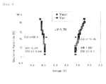
- Fig. 4 is a graph that illustrates an accumulation distribution of a set voltage and a reset voltage when a resistance RAM according to a Preparation Example is repeatedly switched.
- the set voltage is an application voltage that is required to change a state of an element to a low resistance state
- the reset voltage is an application voltage that is required to change a state of an element to a high resistance state.
- the set voltages showed the average value of 1.062 V and the standard deviation of 0.11, and the reset voltages showed the average value of -0.526 V and the standard deviation of 0.11.
- the set voltage and the reset voltage had the uniform distribution, and a difference between the set voltage and the reset voltage was 1.59 V.
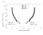
- the log value of the resistance at the low resistance state means the average value of 3.34 and the standard deviation of 0.31
- the log value of the resistance at the high resistance state means the average value of 6.65 and the standard deviation of 0.40.
- Fig. 6 is a graph that illustrates a current change according to the number of voltage pulse that is applied to the resistance RAM according to a Preparation Example.
- the resistance was read at 0.2 V.
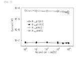
- Fig. 7 is a graph that illustrates a high temperature data maintenance characteristic with respects to the resistance RAM according to a Preparation Example.
- the resistance RAM according to Preparation Example was formed to the low resistance state (or high resistance state), it was left at 85°C (or 125°C) for 10 sec, 100 sec, 1000 sec, and 10000 sec, and the current was measured and shown.
- Fig. 8 is a graph that illustrates yields of the resistance RAMs according to Preparation Examples and Comparative Examples.
- the resistance RAM according to Preparation Example has almost the similar value to the yield of the resistance RAM (Comparative Example 1) that is provided with the STO layer (Nb:STO) that is doped with Nb and is the single crystal layer as the resistance change layer. This may be caused by the uniform formation of the conductive filament in the resistance RAM according to Preparation Example.
Landscapes
- Chemical & Material Sciences (AREA)
- Crystallography & Structural Chemistry (AREA)
- Semiconductor Memories (AREA)
- Electrochromic Elements, Electrophoresis, Or Variable Reflection Or Absorption Elements (AREA)
- Conductive Materials (AREA)
Abstract
Description
- The present invention relates to a nonvolatile RAM, and more particularly, to a resistance RAM.
- Currently, in the case of a flash memory that is commercialized with a nonvolatile memory, an electric charge is stored or removed in an electric charge storage layer, such that a change in threshold voltage is used. The electric charge storage layer may be a floating gate that is a polysilicon layer or an electric charge trap layer that is a silicon nitride layer. Recently, a novel nonvolatile RAM that has low power consumption and high degree of integration as compared to the flash RAM has been studied. As examples of the novel nonvolatile RAMs, there are a phase change RAM, a magnetic RAM and a resistance RAM.
- The resistance RAM may have a structure in which a solid electrolyte layer is inserted between metal electrodes. This element may generate or remove a conductive channel by an electrochemical reaction in the solid electrolyte layer, and two resistance states, that is, a low resistance state and a high resistance state, can be shown in accordance with the presence of the conductive channel. However, it is very difficult to control the formation position and the formation amount of the conductive channel. Accordingly, when the element is switched repeatedly, since resistor distribution of each of the low resistance state and the high resistance state is very large, a nonuniform resistance switching characteristic may be shown, and because of the large resistor distribution of each of the two resistance states, it is difficult to discriminate the two resistance states.
- The present invention has been made keeping in mind the above problems occurring in the related arts, an object of the present invention is to provide a resistance RAM that can lower a resistor distribution.
- The object of the present invention is not limited to the above object, and other objects that are not mentioned may be apparently understood by those skilled in the art from the following description.
- In order to accomplish the object, an aspect of the present invention provides a resistance RAM. The resistance RAM comprises a first electrode, an oxide layer that is formed on the first electrode, a solid electrolyte layer that is disposed on the oxide layer, and a second electrode that is disposed on the solid electrolyte layer.
- A conductive tip that is formed by electrical breakdown may be included in the oxide layer.
- The oxide layer may be a transition metal oxide layer. The transition metal oxide layer may be a lanthanoid oxide layer. The lanthanoid oxide layer may be a gadolinium oxide layer.
- The solid electrolyte layer may includes MoO3-x, W2O3-x, Ta2O5-x, Al2O3-x, HfO2-x, ZrO2-x, CO2O3-x, ZnO1-y, Cu2S, Ag2S or GeSe (x is in the range of 0 to 1.5, y is in the range of 0 to 0.5). The solid electrolyte layer may be a layer that is doped with metal. The metal that is doped in the solid electrolyte layer may be Cu or Ag. The solid electrolyte layer that is doped with the metal may be MoO3-x:Cu, W2O3-x:Cu, Ta2O5-x:Cu, Al2O3-x:Cu, HfO2-x:Cu, ZrO2-x:Cu, CO2O3-x:Cu, ZnO1-x:Cu, MoO3-x:Ag, W2O3-x:Ag, Ta2O5-x:Ag, Al2O3-x:Ag, HfO2-x:Ag, ZrO2-x:Ag, CO2O3-x:Ag, ZnO1-y:Ag, Cu2S:Cu, Ag2S:Ag or GeSe:Ag (x is in the range of 0 to 1.5, y is in the range of 0 to 0.5).
- In order to accomplish the object, an aspect of the present invention provides a method for operating a resistance RAM. The method comprises the step of providing the resistance RAM that comprises a first electrode, an oxide layer that is formed on the first electrode, a solid electrolyte layer that is disposed on the oxide layer, and a second electrode that is disposed on the solid electrolyte layer. A conductive tip is formed in the oxide layer by applying reference voltage to any one of the electrodes, applying foaming voltage to the remain one, such that the oxide layer is electrically broken. A conductive filament is formed in the solid electrolyte layer by applying a positive voltage to the second electrode on the basis of the voltage that is applied to the first electrode. The conductive filament that is formed in the solid electrolyte layer is removed by applying a negative voltage to the second electrode on the basis of the voltage that is applied to the first electrode.
- According to the present invention, the resistance RAM that includes the oxide layer and the solid electrolyte layer as the resistance layer forms a conductive tip in the oxide layer by a foaming process, and may control the position and the number of conductive filaments that are formed in the solid electrolyte layer by concentrating an electric filed at the conductive tip in a reset step. Therefore, in the set step-reset step, that is, in the repeated switching operation between the low resistance state and the high resistance state, since the same conductive filament can be formed or removed, it is possible to ensure the uniform resistance switching characteristic.
-
-
Fig. 1 is a cross-sectional view that illustrates a resistance RAM according to an embodiment of the present invention; -
Fig. 2 is a cross-sectional view that illustrates a foaming step with respects to the resistance RAM according to an embodiment of the present invention; -
Fig. 3A or 3B are a cross-sectional view that illustrates operation method of the resistance RAM according to an embodiment of the present invention; -
Fig. 4 is a graph that illustrates an accumulation distribution of a set voltage and a reset voltage when a resistance RAM according to a Preparation Example is repeatedly switched; -
Fig. 5 is a graph that illustrates a resistance distribution shown in 50 resistance RAMs according to a Preparation Example; -
Fig. 6 is a graph that illustrates a current change according to the number of voltage pulse that is applied to the resistance RAM according to a Preparation Example; -
Fig. 7 is a graph that illustrates a high temperature data maintenance characteristic with respects to the resistance RAM according to a Preparation Example; and -
Fig. 8 is a graph that illustrates yields of the resistance RAMs according to Preparation Examples and Comparative Examples. - In the following detailed description, only certain exemplary embodiments of the present invention have been shown and described, simply by way of illustration. As those skilled in the art would realize, the described embodiments may be modified in various different ways, all without departing from the spirit or scope of the present invention. In the drawings, in the case of when it is mentioned that a layer is provided "on" another layer or a substrate, it may be directly formed on another layer or the substrate or a third layer may be inserted between them.
-
Fig. 1 is a cross-sectional view that illustrates a resistance RAM according to an embodiment of the present invention. - With reference to
Fig. 1 , afirst electrode 11 is formed on asubstrate 10. Thesubstrate 10 may be a silicon substrate or a SOI (Silicon On Insulator) substrate. Before thefirst electrode 11 is formed, after an insulation layer (not shown) is formed on thesubstrate 10, a diffusion prevention layer (not shown) may be formed on an insulation layer. The insulation layer may be a silicon oxide layer, and the diffusion prevention layer may be a titanium layer. - The
first electrode 11 may be a Pt layer, a Ru layer, an Ir layer or an Al layer. - An
oxide layer 13 is formed on thefirst electrode 11. Theoxide layer 13 may be a SiO2, Al2O3, or transition metal oxide layer. The transition metal oxide layer may be a HfO2, ZrO2, Y2O3, or lanthanoid oxide layer. The lanthanoid may be La (Lanthanum), Ce (Cerium), Pr (Praseodymium), Nd (Neodymium), Sm (Samarium), Gd (Gadolinium), or Dy (Dysprosium). The lanthanoid oxide layer may be a gadolinium oxide layer. The gadolinium oxide may be Gd2O3. Theoxide layer 13 may have a thickness that is in the range of 2 to 20 nm. - A
solid electrolyte layer 15 is formed on theoxide layer 13. The resistance value of thesolid electrolyte layer 15 may be 0.1 times or less of the resistance value of theoxide layer 13. Thesolid electrolyte layer 15 means a layer in a solid state having an ion conductivity. Thissolid electrolyte layer 15 may be an amorphous layer. In detail, thesolid electrolyte layer 15 may be a MoO3-x, W2O3-x, Ta2O5-x, Al2O3-x, HfO2-x, ZrO2-x, CO2O3-x, ZnO1-y, Cu2S, Ag2S or GeSe layer. The oxygen atomic ratio of thissolid electrolyte layer 15 may be smaller than a value that satisfies a chemical stoichiometric ratio. That is, thesolid electrolyte layer 15 may be a non-chemical stoichiometric ratio layer that has oxygen vacancy. To this end, x may be in the range of 0 to 1.5, and y may be in the range of 0 to 0.5. Thesolid electrolyte layer 15 has a thickness that is in the range of 30 to 70 nm. - The
solid electrolyte layer 15 may be a layer that contains metal ions therein or is additionally doped with metal ions. The metal that is doped in thesolid electrolyte layer 15 may be Cu or Ag. An example of thesolid electrolyte layer 15 that is doped with the metal may be MoO3-x:Cu, W2O3-x:Cu, Ta2O5-x:Cu, Al2O3-x:Cu, HfO2-x:Cu, ZrO2-x:Cu, CO2O3-x:Cu, ZnO1-x:Cu, MoO3-x:Ag, W2O3-x:Ag, Ta2O5-x:Ag, Al2O3-x:Ag, HfO2-x:Ag, ZrO2-x:Ag, CO2O3-x:Ag, ZnO1-y:Ag, Cu2S:Cu, Ag2S:Ag or GeSe:Ag (x is in the range of 0 to 1.5, and y is in the range of 0 to 0.5). Preferably, thesolid electrolyte layer 15 that is doped with the metal may be the MoO3-x layer that is doped with Cu, that is, the MoO3-x:Cu layer (x is in the range of 0 to 1.5). - The
oxide layer 13 and thesolid electrolyte layer 15 may be formed by using a physical vapor deposition (PVD) method such as a pulsed laser deposition (PLD) method, a thermal evaporation method, an electron-beam evaporation method, a molecular beam epitaxy (MBE) method or a chemical vapor deposition (CVD) method regardless of the correlation between them. - A
second electrode 17 is formed on thesolid electrolyte layer 15. Thesecond electrode 17 may be a Pt layer, a Ru layer, an Ir layer or an Al layer. -
Fig. 2 is a cross-sectional view that illustrates a foaming step with respects to the resistance RAM according to an embodiment of the present invention. - With reference to
Fig. 2 , reference voltage Vr is applied to any one of thefirst electrode 11 and thesecond electrode 17, and the foaming voltage Vf is applied to the remaining electrode. In result, most electric fields are applied to theoxide layer 13 that has large resistance among theoxide layer 13 and thesolid electrolyte layer 15 that are inserted between the electrodes. In result, electrical breakdown occurs in theoxide layer 13, and a region in which conductivity is locally high, that is, aconductive tip 13a that is a conductive path, may be formed. Theconductive tip 13a may have effective area of 10 nm2 or less. - The
conductive tip 13a may be a charged region that is generated by electrically breaking theoxide layer 13, for example, a defect, a phase separation region, or a dislocation. The defect, the phase separation region, or the dislocation may be provided with dangling bonds, such that a conduction path may be formed through the dangling bonds. -
Fig. 3A or 3B are a cross-sectional view that illustrates operation method of the resistance RAM according to an embodiment of the present invention. In detail,Fig. 3A is a cross-sectional view that illustrates a step for setting an element in a low resistance state, andFig. 3B is a cross-sectional view that illustrates a step for resetting an element in a high resistance state. - With reference to
Fig. 3A , a set electric field is applied between thefirst electrode 11 and thesecond electrode 17. In detail, on the basis of the voltage that is applied to thefirst electrode 11, a positive voltage is applied to thesecond electrode 17. For example, reference voltage Vr is applied to thefirst electrode 11, and a positive set voltage Vs is applied to thesecond electrode 17. At this time, the electric filed between the electrodes is concentrated on theconductive tip 13a. In addition, the metal ion in thesolid electrolyte layer 15 is reduced according to the followingReaction Equation 1 by an electron that is supplied from the conductive tip, and forms the metal filament that is connected to theconductive tip 13a.
- At this time, because of the electric field that is concentrated on the
conductive tip 13a, it is possible to control the position and the number (positive) of theconductive filament 15a. In addition, because of the electric field that is concentrated on theconductive tip 13a, even at a low electric field, a conductive filament can be easily formed. - The
conductive filament 15a and theconductive tip 13a provide a conductive path between theelectrodes - With reference to
Fig. 3B , a reset electric field is applied between thefirst electrode 11 and thesecond electrode 17. On the basis of the voltage that is applied to thefirst electrode 11, a negative voltage is applied to thesecond electrode 17. For example, reference voltage Vr is applied to thefirst electrode 11, and a negative reset voltage Vrs is applied to thesecond electrode 17. At this time, the metal particles that constitute theconductive filament 15a are oxidized according to the followingReaction Equation 2.
- Therefore, the
conductive filament 15a is removed, and the conductive path between theelectrodes - As described above, the
conductive tip 13a is formed in theoxide layer 13 by a foaming process, an electric field is concentrated on theconductive tip 13a in a set step, such that it is possible to control the position and the number of theconductive filament 15a. Accordingly, in the set step-reset step, that is, the repeated switching operation between the low resistance state-high resistance state, since the sameconductive filament 15a can be formed or removed, it is possible to ensure the uniform resistance switching characteristic. - Hereinafter, the present invention will be described in detail preferable examples. The present invention may, however, be embodied in many different forms and should not be construed as being limited to the Examples and Experimental Examples set forth herein.
- After the silicon oxide layer and the titanium layer are formed on the silicon substrate, the Pt layer is formed as the first electrode. On the Pt layer, the Gd2O3 layer as the oxide layer was formed in a thickness of 10 nm by using a deposition method. On the Gd2O3 layer, the MoOx layer (X:1.5 - 2.5) that is doped with Cu in an amount of 10 at.%, that is, the Cu:MoOx layer, as the solid electrolyte layer that is doped with the metal ion was formed in a thickness of 50 nm by using a deposition method. On the Cu:MoOx layer, the Pt layer as the second electrode was formed, such that the resistance RAM was prepared.
- After the silicon oxide layer and the titanium layer are formed on the silicon substrate, the Pt layer is formed as the first electrode. On the Pt layer, the STO (Nb:STO) layer that was doped with Nb, which was the single crystal oxide layer, was formed. On the Nb:STO layer, the Pt layer was formed as the second electrode, such that the resistance RAM was prepared.
-
Fig. 4 is a graph that illustrates an accumulation distribution of a set voltage and a reset voltage when a resistance RAM according to a Preparation Example is repeatedly switched. - The set voltage is an application voltage that is required to change a state of an element to a low resistance state, and the reset voltage is an application voltage that is required to change a state of an element to a high resistance state.
- With reference to
Fig. 4 , when the resistance RAM according to Preparation Example is repeatedly switched, the set voltages showed the average value of 1.062 V and the standard deviation of 0.11, and the reset voltages showed the average value of -0.526 V and the standard deviation of 0.11. As described above, even though the repeated switching is carried out, the set voltage and the reset voltage had the uniform distribution, and a difference between the set voltage and the reset voltage was 1.59 V. -
Fig. 5 is a graph that illustrates a resistance distribution shown in 50 resistance RAMs according to a Preparation Example. In detail, after 50 resistance RAMs according to Preparation Example was changed to the low resistance state, the resistance was read at 0.1 V, and after it was changed to the high resistance state, the resistance was read at 0.1 V. - With reference to
Fig. 5 , the log value of the resistance at the low resistance state means the average value of 3.34 and the standard deviation of 0.31, and the log value of the resistance at the high resistance state means the average value of 6.65 and the standard deviation of 0.40. As described above, in a plurality of elements, the resistance distribution at the low resistance state and the resistance distribution at the high resistance state had the uniform distribution. -
Fig. 6 is a graph that illustrates a current change according to the number of voltage pulse that is applied to the resistance RAM according to a Preparation Example. In detail, by alternately applying voltages of -2V (reset voltage) and 2V (set voltage) to the second electrode of Preparation Example, the resistance was read at 0.2 V. - With reference to
Fig. 6 , in the case of when the width of the pulse was 1 µs, which was very short, the current change ratio of 1000 times, that is, the resistance change ratio, was obtained. Accordingly, in the case of when the operation cycle of the element was 1 µs, which was very fast, it can be seen that it is possible to obtain a sufficient switching characteristic. This means that the switching speed is improved. In addition, even though the number of voltage pulse is increased to 10000, the resistance change ratio may not be lowered. This means that the reliability of the element is improved. -
Fig. 7 is a graph that illustrates a high temperature data maintenance characteristic with respects to the resistance RAM according to a Preparation Example. In detail, after the resistance RAM according to Preparation Example was formed to the low resistance state (or high resistance state), it was left at 85°C (or 125°C) for 10 sec, 100 sec, 1000 sec, and 10000 sec, and the current was measured and shown. - With reference to
Fig. 7 , in all conditions of low resistance state/85°C, low resistance state/125°C, high resistance state/85°C, and high resistance state/125°C, it can be seen that data can be maintained until 10000 sec. This means that the high temperature data maintenance characteristic of the resistance RAM according to Preparation Example is excellent. -
Fig. 8 is a graph that illustrates yields of the resistance RAMs according to Preparation Examples and Comparative Examples. - With reference to
Fig. 8 , even though the resistance RAM according to Preparation Example is provided with a solid electrolyte layer that is an amorphous layer and an oxide layer that is a polycrystalline layer, the resistance RAM according to Preparation Example has almost the similar value to the yield of the resistance RAM (Comparative Example 1) that is provided with the STO layer (Nb:STO) that is doped with Nb and is the single crystal layer as the resistance change layer. This may be caused by the uniform formation of the conductive filament in the resistance RAM according to Preparation Example. - Although the preferred embodiments of the present invention have been disclosed for illustrative purposes, those skilled in the art will appreciate that various modifications, additions and substitutions are possible, without departing from the scope and spirit of the invention as disclosed in the accompanying claims.
Claims (10)
- A resistance RAM comprising:a first electrode;an oxide layer that is formed on the first electrode;a solid electrolyte layer that is disposed on the oxide layer; anda second electrode that is disposed on the solid electrolyte layer.
- The resistance RAM according to claim 1, wherein a conductive tip that is formed by electrical breakdown is included in the oxide layer.
- The resistance RAM according to claim 1, wherein the oxide layer is a transition metal oxide layer.
- The resistance RAM according to claim 3, wherein the transition metal oxide layer is a lanthanoid oxide layer.
- The resistance RAM according to claim 4, wherein the lanthanoid oxide layer is a gadolinium oxide layer.
- The resistance RAM according to claim 1, wherein the solid electrolyte layer includes MoO3-x, W2O3-x, Ta2O5-x, Al2O3-x, HfO2-x, ZrO2-x, CO2O3-x, ZnO1-y, Cu2S, Ag2S or GeSe (x is in the range of 0 to 1.5, y is in the range of 0 to 0.5).
- The resistance RAM according to claim 1, wherein the solid electrolyte layer is a layer that is doped with metal.
- The resistance RAM according to claim 7, wherein the metal that is doped in the solid electrolyte layer is Cu or Ag.
- The resistance RAM according to claim 7, wherein the solid electrolyte layer that is doped with the metal is MoO3-x:Cu, W2O3-x:Cu, Ta2O5-x:Cu, Al2O3-x:Cu, HfO2-x:Cu, ZrO2-x:Cu, CO2O3-x:Cu, ZnO1-x:Cu, MoO3-x:Ag, W2O3-x:Ag, Ta2O5-x:Ag, Al2O3-x:Ag, HfO2-x:Ag, ZrO2-x:Ag, CO2O3-x:Ag, ZnO1-y:Ag, Cu2S:Cu, Ag2S:Ag or GeSe:Ag (x is in the range of 0 to 1.5, y is in the range of 0 to 0.5).
- A method for operating a resistance RAM, the method comprising the steps of:providing the resistance RAM that comprises a first electrode, an oxide layer that is formed on the first electrode, a solid electrolyte layer that is disposed on the oxide layer, and a second electrode that is disposed on the solid electrolyte layer;forming a conductive tip in the oxide layer by applying reference voltage to any one of the electrodes, applying foaming voltage to the remain one, such that the oxide layer is electrically broken;forming a conductive filament in the solid electrolyte layer by applying a positive voltage to the second electrode on the basis of the voltage that is applied to the first electrode; andremoving the conductive filament that is formed in the solid electrolyte layer by applying a negative voltage to the second electrode on the basis of the voltage that is applied to the first electrode.
Applications Claiming Priority (1)
| Application Number | Priority Date | Filing Date | Title |
|---|---|---|---|
| KR1020080064487A KR100983175B1 (en) | 2008-07-03 | 2008-07-03 | A resistance change memory device comprising an oxide film and a solid electrolyte film, and an operation method thereof |
Publications (2)
| Publication Number | Publication Date |
|---|---|
| EP2141753A2 true EP2141753A2 (en) | 2010-01-06 |
| EP2141753A3 EP2141753A3 (en) | 2012-09-12 |
Family
ID=41211860
Family Applications (1)
| Application Number | Title | Priority Date | Filing Date |
|---|---|---|---|
| EP09164520A Withdrawn EP2141753A3 (en) | 2008-07-03 | 2009-07-03 | Resistance RAM having oxide layer and solid electrolyte layer, and method for operating the same |
Country Status (4)
| Country | Link |
|---|---|
| US (1) | US8116116B2 (en) |
| EP (1) | EP2141753A3 (en) |
| JP (1) | JP2010016381A (en) |
| KR (1) | KR100983175B1 (en) |
Cited By (6)
| Publication number | Priority date | Publication date | Assignee | Title |
|---|---|---|---|---|
| WO2012044276A1 (en) | 2010-09-27 | 2012-04-05 | Hewlett-Packard Development Company, L.P. | Device structure for long endurance memristors |
| EP2736088A1 (en) * | 2012-11-27 | 2014-05-28 | Commissariat A L'energie Atomique Et Aux Energies Alternatives | Electronic device such as a memory |
| EP2924751A1 (en) * | 2014-03-26 | 2015-09-30 | Commissariat A L'energie Atomique Et Aux Energies Alternatives | Resistive random access memory device |
| WO2015167351A1 (en) * | 2014-04-30 | 2015-11-05 | Nokia Technologies Oy | Memristor and method of production thereof |
| CN108269916A (en) * | 2018-01-07 | 2018-07-10 | 周立伟 | A kind of resistive memory and its manufacturing method |
| EP3843144A1 (en) * | 2019-12-27 | 2021-06-30 | Samsung Electronics Co., Ltd. | Variable resistance memory device |
Families Citing this family (41)
| Publication number | Priority date | Publication date | Assignee | Title |
|---|---|---|---|---|
| KR101096202B1 (en) | 2008-12-29 | 2011-12-22 | 주식회사 하이닉스반도체 | Switching device with solid electrolyte layer |
| JP5716012B2 (en) * | 2009-04-10 | 2015-05-13 | インターモレキュラー,インコーポレーテッド | Resistive switching memory device with improved switching characteristics |
| KR101699769B1 (en) * | 2010-02-08 | 2017-01-25 | 삼성전자주식회사 | Resistance memory devices and methods of forming the same |
| US8415652B2 (en) | 2010-06-21 | 2013-04-09 | Hewlett-Packard Development Company, L.P. | Memristors with a switching layer comprising a composite of multiple phases |
| KR101744758B1 (en) | 2010-08-31 | 2017-06-09 | 삼성전자 주식회사 | Nonvolatile memory element and memory device including the same |
| WO2012057499A2 (en) * | 2010-10-26 | 2012-05-03 | 한양대학교 산학협력단 | Resistive memory having rectifying characteristics or an ohmic contact layer |
| CN102479925A (en) * | 2010-11-30 | 2012-05-30 | 中国科学院微电子研究所 | Resistance transition memory structure with high variable ratio capability and its preparation method |
| JP5390715B2 (en) * | 2010-12-01 | 2014-01-15 | キヤノンアネルバ株式会社 | Nonvolatile memory element and manufacturing method thereof |
| CN102136487B (en) * | 2010-12-31 | 2013-09-18 | 中国科学院上海硅酸盐研究所 | Resistance-type RAM (Random Access Memory) memory unit based on zinc oxide material and preparation method thereof |
| US9165645B2 (en) * | 2011-06-24 | 2015-10-20 | Hewlett-Packard Development Company, L.P. | High-reliability high-speed memristor |
| WO2013009316A1 (en) * | 2011-07-14 | 2013-01-17 | Hewlett-Packard Development Company, L.P. | Memristors having mixed oxide phases |
| JP5548170B2 (en) | 2011-08-09 | 2014-07-16 | 株式会社東芝 | Resistance change memory and manufacturing method thereof |
| JP5687978B2 (en) * | 2011-09-14 | 2015-03-25 | ルネサスエレクトロニクス株式会社 | Resistance variable nonvolatile memory device, semiconductor device, and resistance variable nonvolatile memory operating method |
| JP5537524B2 (en) * | 2011-09-22 | 2014-07-02 | 株式会社東芝 | Resistance change memory |
| KR101356958B1 (en) | 2012-04-10 | 2014-01-29 | 성균관대학교산학협력단 | Resistive random access memory devices and methods of manufacturing the resistive random access memory devices |
| KR101508423B1 (en) * | 2012-04-30 | 2015-04-07 | 주식회사 엘지화학 | Oxide solid electrolyte doped lithium metal, preparation method of thereof, and lithium secondary battery comprsing the same |
| US8558209B1 (en) | 2012-05-04 | 2013-10-15 | Micron Technology, Inc. | Memory cells having-multi-portion data storage region |
| JP5783961B2 (en) * | 2012-07-09 | 2015-09-24 | 株式会社東芝 | Nonvolatile memory device |
| JP5810056B2 (en) * | 2012-09-10 | 2015-11-11 | 株式会社東芝 | Storage device |
| JP2014056888A (en) | 2012-09-11 | 2014-03-27 | Toshiba Corp | Storage device |
| KR20140035558A (en) | 2012-09-14 | 2014-03-24 | 삼성전자주식회사 | Variable resistance memory device and method of forming the same |
| FR2998704A1 (en) * | 2012-11-27 | 2014-05-30 | Commissariat Energie Atomique | Electronic device i.e. conductive bridging RAM, has electrolyte, where volume of electrolyte is selected such that surface of end of electrolyte in contact with electrode is strictly lower than surface of another end of electrolyte |
| US8907314B2 (en) | 2012-12-27 | 2014-12-09 | Intermolecular, Inc. | MoOx-based resistance switching materials |
| US9047940B2 (en) | 2013-01-10 | 2015-06-02 | Intermolecular, Inc. | Resistive random access memory cells having variable switching characteristics |
| KR101439530B1 (en) * | 2013-02-26 | 2014-09-17 | 고려대학교 산학협력단 | light receiving device having transparent electrode and manufacturing method of the same |
| US9000407B2 (en) | 2013-05-28 | 2015-04-07 | Intermolecular, Inc. | ReRAM materials stack for low-operating-power and high-density applications |
| JP6191986B2 (en) * | 2013-06-27 | 2017-09-06 | 国立研究開発法人物質・材料研究機構 | Variable electric conduction element using all-solid electric double layer and electronic device using the same |
| KR101436748B1 (en) * | 2013-06-29 | 2014-09-02 | 고려대학교 산학협력단 | Structure of solid electrolyte electrode, method of forming a structure of solid electrolyte electrode and resistor-variable switching device |
| JP5686219B2 (en) * | 2013-07-01 | 2015-03-18 | 富士ゼロックス株式会社 | Method of designing tip shape of cutting member and method of manufacturing semiconductor piece |
| EP3213348B1 (en) | 2014-09-30 | 2019-07-03 | Hewlett-Packard Development Company, L.P. | Memristors with oxide switching layers |
| CN107004766A (en) * | 2014-11-26 | 2017-08-01 | 密克罗奇普技术公司 | The resistive memory cell of spacer regions with the electric field for reduced conductive path area/enhanced |
| CN105789433A (en) * | 2014-12-25 | 2016-07-20 | 北京有色金属研究总院 | Resistive random access memory and manufacturing method therefor |
| CN106410024A (en) * | 2015-08-03 | 2017-02-15 | 华邦电子股份有限公司 | Resistive random access memory |
| US10516104B2 (en) | 2015-09-25 | 2019-12-24 | Intel Corporation | High retention resistive random access memory |
| CN106711326A (en) * | 2015-11-18 | 2017-05-24 | 北京北方微电子基地设备工艺研究中心有限责任公司 | Resistive random access memory and preparation method thereof, |
| US10497871B2 (en) | 2015-12-26 | 2019-12-03 | Intel Corporation | High retention resistive random access memory |
| US20190181337A1 (en) * | 2016-09-25 | 2019-06-13 | Intel Corporation | Barriers for metal filament memory devices |
| WO2018057021A1 (en) * | 2016-09-25 | 2018-03-29 | Intel Corporation | Metal filament memory cells |
| KR101945814B1 (en) | 2017-12-20 | 2019-02-08 | 성균관대학교산학협력단 | Resistance random access memory device and preparing method thereof |
| CN114005935B (en) * | 2021-10-29 | 2025-09-02 | 复旦大学 | Oxygen vacancy and ion heterogeneous integration of neural synaptic memristor and preparation method thereof |
| KR102810371B1 (en) * | 2022-04-25 | 2025-05-21 | 울산과학기술원 | Threshold switching selector device and fabrication method of the same |
Family Cites Families (37)
| Publication number | Priority date | Publication date | Assignee | Title |
|---|---|---|---|---|
| JP2000028563A (en) | 1998-07-14 | 2000-01-28 | Canon Inc | Humidity sensor and humidity measurement method |
| KR100753612B1 (en) * | 2001-05-09 | 2007-08-29 | 에스케이케미칼주식회사 | Solid Electrolytic Capacitors and Manufacturing Method Thereof |
| US7750332B2 (en) * | 2002-04-30 | 2010-07-06 | Japan Science And Technology Agency | Solid electrolyte switching device, FPGA using same, memory device, and method for manufacturing solid electrolyte switching device |
| JP4792714B2 (en) * | 2003-11-28 | 2011-10-12 | ソニー株式会社 | Storage element and storage device |
| JP2005167064A (en) * | 2003-12-04 | 2005-06-23 | Sharp Corp | Nonvolatile semiconductor memory device |
| DE102004011431B4 (en) * | 2004-03-09 | 2007-09-27 | Infineon Technologies Ag | Method for producing a non-volatile semiconductor memory |
| US7190048B2 (en) * | 2004-07-19 | 2007-03-13 | Micron Technology, Inc. | Resistance variable memory device and method of fabrication |
| JP4830275B2 (en) * | 2004-07-22 | 2011-12-07 | ソニー株式会社 | Memory element |
| KR100697282B1 (en) * | 2005-03-28 | 2007-03-20 | 삼성전자주식회사 | Resistive memory cell, formation method thereof and resistor memory array using same |
| KR20070075812A (en) * | 2006-01-16 | 2007-07-24 | 삼성전자주식회사 | Resistive memory device including an amorphous solid electrolyte layer in a storage node |
| KR100718155B1 (en) * | 2006-02-27 | 2007-05-14 | 삼성전자주식회사 | Nonvolatile Memory Device Using Two Oxide Layers |
| KR101176543B1 (en) * | 2006-03-10 | 2012-08-28 | 삼성전자주식회사 | Resistance Random Memory Device |
| US20070267621A1 (en) * | 2006-05-19 | 2007-11-22 | Infineon Technologies Ag | Resistive memory device |
| JP4869006B2 (en) * | 2006-09-27 | 2012-02-01 | 株式会社東芝 | Method for controlling semiconductor memory device |
| WO2008038365A1 (en) * | 2006-09-28 | 2008-04-03 | Fujitsu Limited | Variable-resistance element |
| US7724562B2 (en) * | 2006-11-02 | 2010-05-25 | The Board Of Trustees Of The Leland Stanford Junior University | Electrochemical memory with heater |
| WO2008062623A1 (en) * | 2006-11-22 | 2008-05-29 | Nec Corporation | Nonvolatile storage device |
| US7728405B2 (en) * | 2007-03-08 | 2010-06-01 | Qimonda Ag | Carbon memory |
| US20080247214A1 (en) * | 2007-04-03 | 2008-10-09 | Klaus Ufert | Integrated memory |
| US20080273370A1 (en) * | 2007-05-02 | 2008-11-06 | Jan Keller | Integrated Circuit, Method of Operating an Integrated Circuit, Memory Cell Array, and Memory Module |
| TWI402980B (en) * | 2007-07-20 | 2013-07-21 | Macronix Int Co Ltd | Resistive memory structure with buffer layer |
| JP2009043905A (en) * | 2007-08-08 | 2009-02-26 | Hitachi Ltd | Semiconductor device |
| JP5175525B2 (en) * | 2007-11-14 | 2013-04-03 | 株式会社東芝 | Nonvolatile semiconductor memory device |
| US20090140232A1 (en) * | 2007-11-30 | 2009-06-04 | Klaus-Dieter Ufert | Resistive Memory Element |
| JP4466738B2 (en) * | 2008-01-09 | 2010-05-26 | ソニー株式会社 | Storage element and storage device |
| JP2009246085A (en) * | 2008-03-31 | 2009-10-22 | Hitachi Ltd | Semiconductor device, and method of manufacturing the same |
| US20090272958A1 (en) * | 2008-05-02 | 2009-11-05 | Klaus-Dieter Ufert | Resistive Memory |
| US8742387B2 (en) * | 2008-06-25 | 2014-06-03 | Qimonda Ag | Resistive memory devices with improved resistive changing elements |
| US7852660B2 (en) * | 2008-10-08 | 2010-12-14 | Seagate Technology Llc | Enhancing read and write sense margins in a resistive sense element |
| US8022547B2 (en) * | 2008-11-18 | 2011-09-20 | Seagate Technology Llc | Non-volatile memory cells including small volume electrical contact regions |
| US20100123117A1 (en) * | 2008-11-19 | 2010-05-20 | Seagate Technology Llc | Non volatile memory cells including a filament growth layer and methods of forming the same |
| KR101083643B1 (en) * | 2008-12-29 | 2011-11-16 | 주식회사 하이닉스반도체 | Resistive memory device and manufacturing method thereof |
| TWI394231B (en) * | 2009-02-03 | 2013-04-21 | Nanya Technology Corp | Non-volatile memory cell and fabrication method thereof |
| EP2259267B1 (en) * | 2009-06-02 | 2013-08-21 | Imec | Method for manufacturing a resistive switching memory cell comprising a nickel oxide layer operable at low-power and memory cells obtained thereof |
| US7965538B2 (en) * | 2009-07-13 | 2011-06-21 | Seagate Technology Llc | Active protection device for resistive random access memory (RRAM) formation |
| US8227783B2 (en) * | 2009-07-13 | 2012-07-24 | Seagate Technology Llc | Non-volatile resistive sense memory with praseodymium calcium manganese oxide |
| US20110084248A1 (en) * | 2009-10-13 | 2011-04-14 | Nanya Technology Corporation | Cross point memory array devices |
-
2008
- 2008-07-03 KR KR1020080064487A patent/KR100983175B1/en not_active Expired - Fee Related
-
2009
- 2009-06-29 US US12/494,212 patent/US8116116B2/en not_active Expired - Fee Related
- 2009-07-03 JP JP2009158437A patent/JP2010016381A/en active Pending
- 2009-07-03 EP EP09164520A patent/EP2141753A3/en not_active Withdrawn
Cited By (18)
| Publication number | Priority date | Publication date | Assignee | Title |
|---|---|---|---|---|
| US8872153B2 (en) | 2010-09-27 | 2014-10-28 | Hewlett-Packard Development Company, L.P. | Device structure for long endurance memristors |
| CN103180949A (en) * | 2010-09-27 | 2013-06-26 | 惠普发展公司,有限责任合伙企业 | Device structure for long endurance memristors |
| EP2622664A4 (en) * | 2010-09-27 | 2013-08-07 | Hewlett Packard Development Co | DEVICE STRUCTURE FOR HIGH-STRENGTH MEMORISTS |
| CN103180949B (en) * | 2010-09-27 | 2016-10-05 | 慧与发展有限责任合伙企业 | The device structure of the memristor of long endurance |
| WO2012044276A1 (en) | 2010-09-27 | 2012-04-05 | Hewlett-Packard Development Company, L.P. | Device structure for long endurance memristors |
| FR2998708A1 (en) * | 2012-11-27 | 2014-05-30 | Commissariat Energie Atomique | ELECTRONIC DEVICE OF MEMORY TYPE |
| US9209391B2 (en) | 2012-11-27 | 2015-12-08 | Commissariat A L'energie Atomique Et Aux Energies Alternatives | Electronic memory device having an electrode made of a soluble material |
| EP2736088A1 (en) * | 2012-11-27 | 2014-05-28 | Commissariat A L'energie Atomique Et Aux Energies Alternatives | Electronic device such as a memory |
| EP2924751A1 (en) * | 2014-03-26 | 2015-09-30 | Commissariat A L'energie Atomique Et Aux Energies Alternatives | Resistive random access memory device |
| FR3019376A1 (en) * | 2014-03-26 | 2015-10-02 | Commissariat Energie Atomique | RESISTIVE LIFE MEMORY DEVICE |
| US9431607B2 (en) | 2014-03-26 | 2016-08-30 | Commissariat à l'énergie atomique et aux énergies alternatives | Metal-oxide-based conductive-bridging random access memory (CBRAM) having the solid electrolyte doped with a second metal |
| WO2015167351A1 (en) * | 2014-04-30 | 2015-11-05 | Nokia Technologies Oy | Memristor and method of production thereof |
| WO2015167357A1 (en) * | 2014-04-30 | 2015-11-05 | Nokia Technologies Oy | Memristor and method of production thereof |
| US9978940B2 (en) | 2014-04-30 | 2018-05-22 | Provenance Asset Group Llc | Memristor and method of production thereof |
| CN108269916A (en) * | 2018-01-07 | 2018-07-10 | 周立伟 | A kind of resistive memory and its manufacturing method |
| EP3843144A1 (en) * | 2019-12-27 | 2021-06-30 | Samsung Electronics Co., Ltd. | Variable resistance memory device |
| US11575084B2 (en) | 2019-12-27 | 2023-02-07 | Samsung Electronics Co., Ltd. | Variable resistance memory device |
| US12527239B2 (en) | 2019-12-27 | 2026-01-13 | Samsung Electronics Co., Ltd. | Variable resistance memory device |
Also Published As
| Publication number | Publication date |
|---|---|
| KR100983175B1 (en) | 2010-09-20 |
| JP2010016381A (en) | 2010-01-21 |
| US20100002491A1 (en) | 2010-01-07 |
| KR20100004363A (en) | 2010-01-13 |
| EP2141753A3 (en) | 2012-09-12 |
| US8116116B2 (en) | 2012-02-14 |
Similar Documents
| Publication | Publication Date | Title |
|---|---|---|
| US8116116B2 (en) | Resistance RAM having oxide layer and solid electrolyte layer, and method for operating the same | |
| Gao et al. | Forming-free and self-rectifying resistive switching of the simple Pt/TaO x/n-Si structure for access device-free high-density memory application | |
| US8987699B2 (en) | Conductive bridge resistive memory device and method of manufacturing the same | |
| KR101613033B1 (en) | Resistance change memory | |
| US20140014890A1 (en) | Conductive path in switching material in a resistive random access memory device and control | |
| US10950384B2 (en) | Method used in forming an electronic device comprising conductive material and ferroelectric material | |
| CN103168372A (en) | Composition of memory cell with resistance-switching layers | |
| JP5544621B2 (en) | Electrochemical transistor | |
| US11004506B2 (en) | Switching resistor and method of making such a device | |
| US12382846B2 (en) | Ferroelectric components and cross point array devices including the ferroelectric components | |
| US8487289B2 (en) | Electrically actuated device | |
| US10084015B2 (en) | Resistive memory element employing electron density modulation and structural relaxation | |
| US12114581B2 (en) | Magnesium ion based synaptic device | |
| KR100969807B1 (en) | Resistance change memory device having a reactive metal film and a method of operating the same | |
| US20120091418A1 (en) | Bipolar storage elements for use in memory cells and methods of forming the same | |
| US20110175052A1 (en) | Resistance-variable memory device including carbide-based solid electrolyte membrane and manufacturing method thereof | |
| WO2022127383A1 (en) | In-memory resistive random access memory xor logic using complimentary switching | |
| WO2007004807A1 (en) | Memory device using abrupt metal-insulator transition and method of operating the same | |
| KR100986018B1 (en) | Forming Method of Resistance Change Memory Device and Resistance Change Memory Device | |
| Mordvintsev et al. | Effect of constructional features of the insulating gap of open TiN–SiO2–W and Si–SiO2–W “sandwich” structures on the process of their electroforming | |
| KR101069124B1 (en) | Nonvolatile Resistance Change Memory Device | |
| Zhang et al. | Modeling of conducting bridge evolution in bipolar vanadium oxide-based resistive switching memory | |
| US20260075832A1 (en) | Electrochemical memory device and driving method thereof | |
| Jin et al. | An investigation of CeO2 based ReRAM with p+ and n+-Si bottom electrodes | |
| KR100644869B1 (en) | Nonvolatile Memory Using Resistance Change of Crystalline Oxide |
Legal Events
| Date | Code | Title | Description |
|---|---|---|---|
| PUAI | Public reference made under article 153(3) epc to a published international application that has entered the european phase |
Free format text: ORIGINAL CODE: 0009012 |
|
| 17P | Request for examination filed |
Effective date: 20090703 |
|
| AK | Designated contracting states |
Kind code of ref document: A2 Designated state(s): AT BE BG CH CY CZ DE DK EE ES FI FR GB GR HR HU IE IS IT LI LT LU LV MC MK MT NL NO PL PT RO SE SI SK SM TR |
|
| PUAL | Search report despatched |
Free format text: ORIGINAL CODE: 0009013 |
|
| AK | Designated contracting states |
Kind code of ref document: A3 Designated state(s): AT BE BG CH CY CZ DE DK EE ES FI FR GB GR HR HU IE IS IT LI LT LU LV MC MK MT NL NO PL PT RO SE SI SK SM TR |
|
| AX | Request for extension of the european patent |
Extension state: AL BA RS |
|
| RIC1 | Information provided on ipc code assigned before grant |
Ipc: H01L 45/00 20060101AFI20120807BHEP |
|
| RIC1 | Information provided on ipc code assigned before grant |
Ipc: H01L 45/00 20060101AFI20131205BHEP |
|
| GRAP | Despatch of communication of intention to grant a patent |
Free format text: ORIGINAL CODE: EPIDOSNIGR1 |
|
| INTG | Intention to grant announced |
Effective date: 20140122 |
|
| STAA | Information on the status of an ep patent application or granted ep patent |
Free format text: STATUS: THE APPLICATION IS DEEMED TO BE WITHDRAWN |
|
| 18D | Application deemed to be withdrawn |
Effective date: 20140603 |