EP2141728A2 - Image displaying apparatus - Google Patents
Image displaying apparatus Download PDFInfo
- Publication number
- EP2141728A2 EP2141728A2 EP09163656A EP09163656A EP2141728A2 EP 2141728 A2 EP2141728 A2 EP 2141728A2 EP 09163656 A EP09163656 A EP 09163656A EP 09163656 A EP09163656 A EP 09163656A EP 2141728 A2 EP2141728 A2 EP 2141728A2
- Authority
- EP
- European Patent Office
- Prior art keywords
- spacer
- wiring
- displaying apparatus
- image displaying
- resistive
- Prior art date
- Legal status (The legal status is an assumption and is not a legal conclusion. Google has not performed a legal analysis and makes no representation as to the accuracy of the status listed.)
- Withdrawn
Links
- 125000006850 spacer group Chemical group 0.000 claims abstract description 87
- 229910052751 metal Inorganic materials 0.000 claims abstract description 69
- 239000002184 metal Substances 0.000 claims abstract description 69
- 239000000758 substrate Substances 0.000 claims abstract description 29
- 239000011159 matrix material Substances 0.000 claims abstract description 15
- 238000007599 discharging Methods 0.000 abstract description 19
- 230000001105 regulatory effect Effects 0.000 abstract description 13
- 208000028659 discharge Diseases 0.000 description 26
- 238000010586 diagram Methods 0.000 description 21
- 238000000034 method Methods 0.000 description 12
- 238000004519 manufacturing process Methods 0.000 description 8
- 239000011521 glass Substances 0.000 description 6
- 229910052782 aluminium Inorganic materials 0.000 description 5
- XAGFODPZIPBFFR-UHFFFAOYSA-N aluminium Chemical compound [Al] XAGFODPZIPBFFR-UHFFFAOYSA-N 0.000 description 5
- 230000015556 catabolic process Effects 0.000 description 5
- 238000010894 electron beam technology Methods 0.000 description 5
- 230000005856 abnormality Effects 0.000 description 4
- 239000000203 mixture Substances 0.000 description 4
- 230000002093 peripheral effect Effects 0.000 description 4
- 230000015572 biosynthetic process Effects 0.000 description 3
- 238000001035 drying Methods 0.000 description 3
- 239000000463 material Substances 0.000 description 3
- 238000007639 printing Methods 0.000 description 3
- 238000007740 vapor deposition Methods 0.000 description 3
- 239000004925 Acrylic resin Substances 0.000 description 2
- 229920000178 Acrylic resin Polymers 0.000 description 2
- VYZAMTAEIAYCRO-UHFFFAOYSA-N Chromium Chemical compound [Cr] VYZAMTAEIAYCRO-UHFFFAOYSA-N 0.000 description 2
- OAICVXFJPJFONN-UHFFFAOYSA-N Phosphorus Chemical compound [P] OAICVXFJPJFONN-UHFFFAOYSA-N 0.000 description 2
- 239000003086 colorant Substances 0.000 description 2
- 238000000151 deposition Methods 0.000 description 2
- 238000005530 etching Methods 0.000 description 2
- 230000006698 induction Effects 0.000 description 2
- 238000010030 laminating Methods 0.000 description 2
- 239000007788 liquid Substances 0.000 description 2
- 230000000873 masking effect Effects 0.000 description 2
- 239000011295 pitch Substances 0.000 description 2
- 238000005488 sandblasting Methods 0.000 description 2
- 238000007650 screen-printing Methods 0.000 description 2
- 208000016169 Fish-eye disease Diseases 0.000 description 1
- BPQQTUXANYXVAA-UHFFFAOYSA-N Orthosilicate Chemical compound [O-][Si]([O-])([O-])[O-] BPQQTUXANYXVAA-UHFFFAOYSA-N 0.000 description 1
- 229910000831 Steel Inorganic materials 0.000 description 1
- RTAQQCXQSZGOHL-UHFFFAOYSA-N Titanium Chemical compound [Ti] RTAQQCXQSZGOHL-UHFFFAOYSA-N 0.000 description 1
- NIXOWILDQLNWCW-UHFFFAOYSA-N acrylic acid group Chemical group C(C=C)(=O)O NIXOWILDQLNWCW-UHFFFAOYSA-N 0.000 description 1
- 239000003513 alkali Substances 0.000 description 1
- 239000011230 binding agent Substances 0.000 description 1
- 229910000416 bismuth oxide Inorganic materials 0.000 description 1
- 239000011248 coating agent Substances 0.000 description 1
- 238000000576 coating method Methods 0.000 description 1
- TYIXMATWDRGMPF-UHFFFAOYSA-N dibismuth;oxygen(2-) Chemical compound [O-2].[O-2].[O-2].[Bi+3].[Bi+3] TYIXMATWDRGMPF-UHFFFAOYSA-N 0.000 description 1
- 238000009792 diffusion process Methods 0.000 description 1
- 238000009826 distribution Methods 0.000 description 1
- 230000005684 electric field Effects 0.000 description 1
- 239000000839 emulsion Substances 0.000 description 1
- 238000000227 grinding Methods 0.000 description 1
- 238000012986 modification Methods 0.000 description 1
- 230000004048 modification Effects 0.000 description 1
- 230000000149 penetrating effect Effects 0.000 description 1
- 235000019353 potassium silicate Nutrition 0.000 description 1
- 239000000843 powder Substances 0.000 description 1
- 230000000452 restraining effect Effects 0.000 description 1
- 229910001925 ruthenium oxide Inorganic materials 0.000 description 1
- WOCIAKWEIIZHES-UHFFFAOYSA-N ruthenium(iv) oxide Chemical compound O=[Ru]=O WOCIAKWEIIZHES-UHFFFAOYSA-N 0.000 description 1
- 238000009751 slip forming Methods 0.000 description 1
- 238000005507 spraying Methods 0.000 description 1
- 239000010959 steel Substances 0.000 description 1
- 239000010936 titanium Substances 0.000 description 1
- 229910052719 titanium Inorganic materials 0.000 description 1
Images



Classifications
-
- H—ELECTRICITY
- H01—ELECTRIC ELEMENTS
- H01J—ELECTRIC DISCHARGE TUBES OR DISCHARGE LAMPS
- H01J31/00—Cathode ray tubes; Electron beam tubes
- H01J31/08—Cathode ray tubes; Electron beam tubes having a screen on or from which an image or pattern is formed, picked up, converted, or stored
- H01J31/10—Image or pattern display tubes, i.e. having electrical input and optical output; Flying-spot tubes for scanning purposes
- H01J31/12—Image or pattern display tubes, i.e. having electrical input and optical output; Flying-spot tubes for scanning purposes with luminescent screen
- H01J31/123—Flat display tubes
- H01J31/125—Flat display tubes provided with control means permitting the electron beam to reach selected parts of the screen, e.g. digital selection
- H01J31/127—Flat display tubes provided with control means permitting the electron beam to reach selected parts of the screen, e.g. digital selection using large area or array sources, i.e. essentially a source for each pixel group
-
- H—ELECTRICITY
- H01—ELECTRIC ELEMENTS
- H01J—ELECTRIC DISCHARGE TUBES OR DISCHARGE LAMPS
- H01J29/00—Details of cathode-ray tubes or of electron-beam tubes of the types covered by group H01J31/00
- H01J29/02—Electrodes; Screens; Mounting, supporting, spacing or insulating thereof
- H01J29/08—Electrodes intimately associated with a screen on or from which an image or pattern is formed, picked-up, converted or stored, e.g. backing-plates for storage tubes or collecting secondary electrons
- H01J29/085—Anode plates, e.g. for screens of flat panel displays
Definitions
- the present invention relates to an image displaying apparatus, and, more specifically to a constitution of a face plate.
- an image displaying apparatus which comprises a rear plate having plural electron-emitting devices arranged two-dimensionally and a face plate having plural light-emitting members arranged two dimensionally and oppositely to the plural electron-emitting devices has been known.
- the face plate and the rear plate are mutually supported generally by a spacer so as to be opposite to each other at a gap of about several millimeters.
- high voltage e.g., approximately 10kV is applied between the face plate and the rear plate. Consequently, a discharge occurs easily between the face plate and the rear plate, and, if the discharge once occurs, a discharging current flows into the whole of a metal back which has been united overall, whereby an influence to the electron-emitting devices expands.
- Japanese Patent Application Laid-Open No. 2006-120622 (corresponding to U. S. Patent Application Publication No. US2006/0061258 ) discloses a technique for suppressing a discharging current flowing in the unlikely event of a discharge by two-dimensionally divided metal backs and striped resistors.
- each column of the striped resistors is connected only to corresponding each column of the divided metal backs. Therefore, even if a discharge occurs on a certain column, it is possible to restrain the discharging current from flowing into another column.
- Japanese Patent Application Laid-Open No. 2006-126260 (corresponding to U. S. Patent Application Publication No. US2007/0236150 ) discloses a technique for restraining halation from occurring by forming a supporting member made of an insulative material on the surface of a face plate and further forming an intermediate electrode on the formed supporting member.
- a supporting member made of an insulative material on the surface of a face plate
- an intermediate electrode on the formed supporting member.
- the electrons reflected on the surface of the face plate can be captured.
- Japanese Patent Application Laid-Open No. 2006-126260 discloses a technique for providing the intermediate electrode between the face plate and the rear plate.
- the present invention has been completed in consideration of the above-described related art, and aims to provide an image displaying apparatus which simultaneously suppresses both halation and a discharging current flowing in the unlikely event of a discharge, and in which potential regulating for a spacer can be easily performed.
- An image displaying apparatus is characterized by comprising: a rear plate that has plural electron-emitting devices arranged in matrix; a face plate that has a substrate, plural light-emitting members arranged in matrix on the substrate, plural metal backs each of which covers at least the one light-emitting member and which are mutually arranged in matrix at gaps, ribs which have first striped portions respectively positioned among the plural light-emitting members and protruding toward the rear plate, and a resistive wiring which includes a resistor positioned between the substrate and the ribs and electrically connecting the plural metal backs to others, and that is positioned oppositely to the rear plate; and a spacer that is positioned between the rear plate and the ribs to mutually support the rear plate and the face plate, wherein the rib has, on its surface, a spacer connection wiring which abuts against the spacer, and wherein the spacer connection wiring is electrically connected to the resistive wiring.
- the metal backs are arranged two-dimensionally, and each of the metal backs covers at least one light-emitting member.
- the metal backs are divided two-dimensionally, it is possible to easily suppress a discharging current flowing in the unlikely event of a discharge.
- the metal backs cover the light-emitting members and the ribs having the first striped portions extend among the light-emitting members, it is possible to provide the plural ribs as preventing interference with the light-emitting members. Consequently, since halation can be suppressed, it is possible to provide the image displaying apparatus of which the color reproducibility is excellent.
- the spacer connection wiring which extends from the resistive wiring to the top surface of the rib is provided on the side wall of the rib, it is unnecessary to provide an independent wiring to be used for the purpose of potential regulating for the spacer. Consequently, it is possible to perform the potential regulating for the spacer by the simple-constitution spacer connecting wiring.
- the image displaying apparatus which simultaneously suppresses both the halation and the discharging current flowing in the unlikely event of the discharge, and in which the potential regulating for the spacer can be easily performed.
- FIG. 1 is a partial fractured perspective diagram illustrating a basic constitution of an image displaying apparatus according to an embodiment of the present invention.
- FIGS. 2A, 2B and 2C are detailed diagrams illustrating a face plate of the image displaying apparatus illustrated in FIG. 1 .
- FIGS. 3A, 3B and 3C are detailed diagrams illustrating a face plate of an image displaying apparatus according to the second embodiment of the present invention.
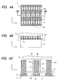
- FIGS. 4A, 4B and 4C are detailed diagrams illustrating a face plate of an image displaying apparatus according to the third embodiment of the present invention.
- FIGS. 5A and 5B are detailed diagrams illustrating a face plate of an image displaying apparatus according to the fourth embodiment of the present invention.
- an image displaying apparatus is applicable to an electron beam displaying apparatus such as a CRT (Cathode Ray Tube), an FED (Field Emission Display) or the like.
- a beam diameter can be easily narrowed down, color reproducibility can be significantly improved by suppressing halation.
- a space between an anode and a cathode becomes a state of high electrical field in the FED, a withstand discharge capability is required. Therefore, the FED is a preferable conformation to which the present invention is applied.
- FIG. 1 is a partial fractured perspective diagram illustrating a basic structure of an image displaying apparatus according to the embodiment of the present invention.
- An image displaying apparatus 21 has a rear plate 9, which has two-dimensionally arranged plural surface conduction electron-emitting devices 13, and a face plate 1, which is arranged oppositely to the rear plate 9.
- the face plate 1 and the rear plate 9 form a vacuum envelope 15 together with an outer frame 14.
- the space 16 is made by a high resistive member through which a small amount of current can be flowed for an antistatic purpose.
- the image displaying apparatus 21 is constituted by further adding a power supply, a driver circuit and the like, which are not illustrated, to the vacuum envelope 15.
- the rear plate 9 has a glass substrate 10, scanning wirings 11 and signal wirings 12 respectively formed on the glass substrate 10, and the surface conduction electron-emitting devices 13 also formed on the glass substrate 10.
- the number of the scanning wirings 11 is N and the number of the signal wirings 12 is M, and the N ⁇ M surface conduction electron-emitting devices 12 are formed in matrix.
- FIGS. 2A, 2B and 2C are detailed diagrams illustrating the face plate of the image displaying apparatus illustrated in FIG. 1 . More specifically, FIG. 2A is the internal diagram of the face plate, FIG. 2B is the cross section diagram along the line 2B-2B in FIG. 2A, and FIG. 2C is the partial enlarged diagram of FIG. 2B . In the following, the constitution of the face plate will be described with reference to FIGS. 2A, 2B and 2C .
- the face plate 1 has a substrate 2. It is preferable to use a glass substrate for the substrate 2 especially in a point that the vacuum performance is maintained and the intensity is ensured.
- a black member 3 is provided on the substrate 2.
- the black member 3, which has apertures, is formed in a lattice-like shape.
- Light-emitting members 4 consisted of phosphors are formed on the apertures.
- the light-emitting members 4 are color-coded by R (Red), G (Green) and B (Blue) so as to cope with color displaying.
- the color-coding pattern can be arbitrarily determined in accordance with display characteristics and that pattern is not limited specifically.
- the plural light-emitting members 4, which are provided oppositely to the plural surface conduction electron-emitting devices 13 are arranged and formed in matrix on the substrate 2.
- plural metal backs 5, each of which covers at least one light-emitting member 4 and which are mutually arranged in matrix at gaps, are provided on the substrate 2.
- the metal backs 5 are divided for each aperture, namely, each sub pixel (e.g., R in RGB).
- the metal backs 5 can be patterned through masking or etching, by means of a known film forming method. In particular, it is preferable to form the metal backs 5 through mask vapor deposition because it is simple.
- the metal backs 5 are divided like lattices, the partial metal backs 5 which are adjacent to each other may be continuously formed.
- the ribs 6 include first striped portions 61 which are positioned among the plural light-emitting members 4 and protrude toward the rear plate 9 (i.e., in the Z direction).
- the first striped portion 61 is the generic term which implies the plural protrusions extending in the Y direction.
- the rib 6 supports the spacer 16 through a later-described spacer connection wiring 8 on its top surface 22. More specifically, the rib 6 is provided on the edge of the black member 3 extending in the Y direction, namely, between the divided adjacent metal backs 5.
- the height of the rib 6 is suitably selected based on a pixel size, an anode voltage and the like.
- the ribs 6 can be formed by a known manufacturing method such as a laminating manufacturing method of laminating pattern prints, a blast manufacturing method for a thick film, a slit coating manufacturing method, or the like. In particular, it is preferable to manufacture the ribs 6 by the blast manufacturing method in terms of productivity, accuracy, and large screen application.
- resistive wirings (feeding wirings) 7, which supply anode potential to the metal backs 5 and electrically connect the plural metal backs 5 mutually, are provided on the substrate 2.
- the resistive wiring 7 is positioned between the substrate 2 and the rib 6, and extends in the Y direction between the rib 6 and the black member 3. Further, the resistive wiring 7 is made by a resistor for suppressing a discharging current flowing in the unlikely event of a discharge.
- the resistive wiring 7 is provided for each column of the metal backs 5, and only an edge portion 24 of one side of the resistive wiring 7 is exposed from the rib 6 in the Y direction along which the resistive wiring 7 extends. Thus, the resistive wiring 7 is electrically connected to the adjacent metal back 5 through the exposed edge portion 24.
- the resistive wirings 7 can be formed by a known manufacturing method such as a pattern printing method, a dispenser method, or the like. In particular, it is preferable to manufacture the resistive wirings 7 by the pattern printing method in terms of accuracy and productivity.
- the spacer connection wiring 8 rises up to the top surface 22 in the direction (Z direction) perpendicular to the substrate 2 on the side wall 23 of the rib 6, and further extends in the direction (Y direction) along which the rib 6 extends on the top surface 22 up to the position abutting against the spacer 16. More specifically, as illustrated in FIG. 2A , the spacer connection wiring 8 extends up to the portion between the metal backs adjacent in the Y direction, whereby the spacer is arranged at this portion (that is, the portion between the metal backs adjacent in the Y direction).
- the spacer 16 is directly connected to the spacer connection wiring 8 on the rib 6, and the resistive wiring 7 and the spacer 16 are electrically connected to each other on the top surface 22 of the rib 6 through the spacer connection wiring 8.
- the rib 6 has on its surface the spacer connection wiring 8 which abuts against the spacer 16, and the spacer connection wiring 8 further abuts against the resistive wiring 7.
- the spacer connection wiring 8 and the resistive wiring 7 are electrically connected to each other. Consequently, it is possible to regulate the spacer 16 to have desired potential.
- the spacer connection wirings 8 can be patterned through masking or etching, by means of a known film forming method. In particular, it is preferable to pattern the spacer connection wirings 8 through mask vapor deposition because it is simple.
- the spacer connection wiring 8 is formed only on the side wall 23 of one side of each rib 6 in regard to the direction (Y direction) through which the rib 6 extends.
- secondary discharge that is, discharge between the metal backs adjacent in the X direction
- a desired discharging current suppressing capability can be achieved. That is, by providing the spacer connection wiring 8 only on the side wall 23 of one side of the rib 6, a creepage distance from the adjacent metal back 5 can be attained. Consequently, in the unlikely event that the discharge occurs, since the short circuit between the adjacent metal backs 5 can be suppressed, the discharging current suppressing capability can be maintained.
- the spacer connection wirings 8 and the metal backs 5 are formed integrally.
- the metal backs 5 and the spacer connection wirings 8 can be simultaneously formed only by pattern-forming the metal backs 5, productivity improves.
- the metal back 5 is electrically connected to a terminal Hv of the vacuum envelope 15, and a high voltage of about 1kV to 15kV is applied by a not-illustrated high voltage power supply.
- the scanning wirings 11 and the signal wirings 12 are respectively connected to terminals Dyn (n denotes positive integers 1 to N) and terminals Dxm (m denotes positive integers 1 to M) of the vacuum envelope 15, and scanning signals and image signals are respectively given to the scanning wirings 11 and the signal wirings 12 by a not-illustrated driver circuit.
- the surface conduction electron-emitting devices 13 emit electrons according to the signals, and the electrons attracted by the metal back potential pass through the metal backs 5 and thus cause the phosphors of the light-emitting members 4 to emit light.
- the luminance can be adjusted according to the voltage or the signals.
- the image displaying apparatus 21 When the image displaying apparatus 21 operates, there is a possibility that so-called halation occurs because some of the electrons are diffused and reflected and further some of the diffused and reflected electrons cause the phosphors to again emit light.
- the halation can be effectively suppressed.
- the metal backs 5 since the metal backs 5 are divided two-dimensionally, the image displaying apparatus which has an excellent withstand discharge function can be provided.
- the side wall 23 of the rib 6 is used as the space for the wirings, the potential regulating for the spacer 16 can be performed only by providing a simple branch constitution (that is, the spacer connection wiring 8) from the resistive wiring 7.
- an independent dedicated resistive line (feeding line) is provided to perform the potential regulating for the spacer 16.
- the lines which are connected to the anode power supply at low resistance increase within the screen. This is not preferable from the aspect of suppressing of a discharging current.
- a through hole is formed inside the rib 6 to perform the potential regulating for the top surface 22 of the rib 6.
- the rib 6 is an insulative member, withstand voltage is necessary between the adjacent metal backs 5. For this reason, if the low-resistance resistive portion is provided inside the rib 6, it is not preferable because there is a possibility that dielectric breakdown occurs.
- the resistive wirings and the spacer connection wirings are arranged regularly in regard to all of the metal backs. Consequently, since the potential distribution can be made substantially even within the image region, displaying characteristics can be made uniform.
- FIGS. 3A, 3B and 3C are detailed diagrams illustrating a face plate of an image displaying apparatus according to the second embodiment. More specifically, FIG. 3A is the internal diagram of the face plate, FIG. 3B is the cross section diagram along the line 3B-3B in FIG. 3A, and FIG. 3C is the cross section diagram along the line 3C-3C in FIG. 3B .
- an abutment of a spacer connection wiring 8a which abuts against a spacer 16 and an abutment of the spacer connection wiring 8a which abuts against a resistive wiring (feeding wiring) 7 are respectively positioned so that they are out of alignment in the direction (Y direction) along which a first striped portion extends. That is, the spacer connection wiring 8a extends at the shortest distance between a metal back 5 and a portion of a rib 6 abutting against the spacer 16.
- FIGS. 4A, 4B and 4C are detailed diagrams illustrating a face plate of an image displaying apparatus according to the third embodiment. More specifically, FIG. 4A is the internal diagram of the face plate, FIG. 4B is the cross section diagram along the line 4B-4B in FIG. 4A, and FIG. 4C is the partial enlarged diagram of FIG. 2B .
- plural ribs 6 are provided, and spacer connection wirings 8b are formed alternately with the ribs 6. More specifically, the spacer connection wiring 8b is formed on both side walls 23 of the alternate rib 6 in the direction (Y direction) along which the rib 6 extends.
- a resistive wiring (feeding wiring) 7b is provided only between the rib 6 on which the spacer connection wiring 8b has been formed and a substrate 2 ( FIG. 4C ). Both edge portions 24 and 25 of the resistive wiring 7b are exposed from the rib 6 in the direction (Y direction) along which the resistive wiring 7b extends, and the resistive wiring 7b is electrically connected to adjacent metal backs 5 at both sides through the exposed edge portions 24 and 25. Thus, the resistive wiring 7b is provided every plural columns of the metal backs 5. As a result, since the bothside metal backs 5 are electrically connected to each other by means of the resistive wiring 7b and the spacer connection wiring 8b, one anode region is formed.
- the present embodiment can provide an effective means for maintaining desired withstand discharge performance according to an anode voltage or a pixel size.
- FIGS. 5A and 5B are detailed diagrams illustrating a face plate of an image displaying apparatus according to the fourth embodiment. More specifically, FIG. 5A is the internal diagram of the face plate, and FIG. 5B is the cross section diagram along the line 5B-5B in FIG. 5A .
- ribs 6c have a lattice shape which includes first striped portions 61a and second striped portions 62 extending in the direction perpendicular to the first striped portions 61a. Consequently, it is preferable because halation can be suppressed two-dimensionally.
- the present embodiment is applicable not only to the third embodiment but also to the first and second embodiments in which the resistive wiring is provided for each column.
- This example is an example of the image displaying apparatus illustrated in FIGS. 1 , 2A, 2B and 2C .
- the face plate of the image displaying apparatus in this example was manufactured as described below. That is, a lattice-like shape, which has apertures only on desired regions of the light-emitting members, was screen-printed on a surface of a cleaned glass substrate by using a black paste (NP-7803D available from Noritake Co., Ltd.), and the obtained glass substrate was baked at 550°C after drying it at 120°C, thereby forming the black member 3 of which the thickness is 5 ⁇ m.
- a black paste NP-7803D available from Noritake Co., Ltd.
- pitches of the aperture portion were set to 450 ⁇ m in the Y direction and 150 ⁇ m in the X direction, as well as device pitches on the rear plate, and the sizes of the aperture portion were set to 220 ⁇ m in the Y direction and 90 ⁇ m in the X direction.
- a high-resistance paste containing ruthenium oxide was formed, as the striped resistive wirings 7, on the pattern extending in the Y direction of the black member 3 by a screen printing method to have the film thickness 10 ⁇ m after the baking. Then, the obtained high-resistance paste was dried at 120°C for 10 minutes.
- the width of the resistive wiring 7 was set to 40 ⁇ m, and the one-side position of the wiring was aligned with the black member 3 of which the thickness is 60 ⁇ m so as to expose the black member of the width 20 ⁇ m. Then, the material used in such a high-resistance layer was applied to a test pattern and the resistance thereof was measured. The obtained volume resistance of this material was about 10 -1 ⁇ m.
- a bismuth oxide insulative paste (NP7753 available from Noritake Co., Ltd.) finally constituting the rib structure was applied by a slit-coater and baked at 120°C for 10 minutes so as to have the film thickness 200 ⁇ m after the baking.
- a DFR dry film resist
- a chrome mask to be used for exposure was aligned to a predetermined position and then the DFR was pattern exposed.
- Such alignment was performed by using a not-illustrated alignment mark provided outside the image formation region.
- the exposing pattern was set to the striped shape of the width 50 ⁇ m (therefore, the width of the aperture portion is 100 ⁇ m) so as to overlap the black member 3, in parallel with the longitudinal edge of the aperture of the black member 3 (that is, extending in the Y direction).
- the resistive wiring 7 was aligned with the aperture edge on the exposing side from the resistive wiring 7 so that the resistive wiring 7 was exposed by 10 ⁇ m in regard to the width 60 ⁇ m of the black member 3. Further, exposure of the DFR, developing, a showering process of rinse liquid and drying are performed, whereby a mask for sand blasting, having apertures on desired positions, was formed. Next, the unnecessary high-resistance paste and the unnecessary insulative paste were eliminated in conformity with the apertures of the DFR by a sand blasting method in which SUS (Stainless Used Steel) grains were used as grinding grains. After then, the DFR was stripped off by a remover liquid shower, and the wirings were cleaned. Next, the wirings were baked at 530°C, whereby the resistive wirings 7 having the ribs 6 and the resistors were formed.
- SUS Stainless Used Steel
- a phosphor was dropped into the light-emitting members and printed by a screen printing method in conformity with the rib structure having the striped apertures by using a paste in which phosphors P22 typically used in the technical field of CRTs (cathode ray tubes) were dispersed.
- the phosphors of three colors R, G and B were separately striped and coated so as to form a color display.
- the thickness of each phosphor was set to 15 ⁇ m.
- the three-color phosphors were dried at 120°C after the printing. Incidentally, the drying may be performed for each color or for all of three colors in a lump. Further, a solution containing contains silicate alkali, so called a liquid glass, acting as a binding agent was applied.
- an acrylic emulsion was applied and dried by the spray coating method, and the spaces in powder phosphors were infilled by acrylic resin.
- an aluminum film acting as the metal back 5 was vapor deposited.
- the metal backs 5 were formed only to the light-emitting members by using a metal mask having the apertures only at the portions corresponding to the respective light-emitting members.
- the thickness of the aluminum film was set to 100nm.
- the spacer connection wirings 8 were formed by vapor depositing the aluminum film obliquely from one direction with use of the metal mask which was striped in the X direction in conformity with the apertures and to be divided in the Y direction.
- the spacer connection wirings 8 may be made not only of aluminum but also of titanium, chrome or the like.
- high-voltage induction terminals penetrating the face plate 1 were provided in the face plate 1 via through holes, and the high-voltage induction terminals were connected at the edge portion of the image formation region with the resistive wirings 7 (not illustrated).
- the image displaying apparatus illustrated in FIG. 1 was manufactured by properly combining the rear plate 9, the outer frame 14 and the conductive spacers 16. At this time, sufficient alignment was performed so that the conductive spacers 16 abut exactly against the spacer connection wirings 8. Then, an image was displayed by applying voltage of 8kV to the metal backs 5 through the resistive wirings 7. In this case, the excellent image in which color mixture due to halation is low could be displayed. Further, since the potential of the spacers was regulated, image distortion based on deviation of the electron beams was not confirmed even in the vicinity of the spacer, whereby an excellent image could be displayed.
- This example corresponds to the second embodiment illustrated in FIGS. 3A to 3C .
- This example is difference from Example 1 in the point concerning a forming pattern of the spacer connection wirings 8. That is, in this example, the spacer connection wiring 8 extends obliquely toward the connecting position with the space on the side wall of the rib 6.
- the spacer connection wirings 8 can be formed simultaneously with the metal backs 5.
- the spacer connection wirings 8 are obtained by performing vapor deposition obliquely in both the X direction and the Y direction by using the metal mask covering the portions other than the necessary portions on the upper surface of the ribs.
- the image displaying apparatus was manufactured by using the face plate 1 thus manufactured, and an image was displayed thereon by applying voltage of 8kV to the metal backs 5 through the resistive wirings 7. In this case, the excellent image in which color mixture due to halation is low could be displayed. Further, since the potential of the spacers was regulated, image distortion based on deviation of the electron beams was not confirmed even in the vicinity of the spacer, whereby an excellent image could be displayed.
- This example corresponds to the third embodiment illustrated in FIGS. 4A to 4C .
- This example is difference from Example 1 in the point that two phosphors adjacent in the X direction are set as one anode region, and the single resistive wiring 7b is arranged between the two phosphors, for one anode region.
- the width of the resistive wiring 7b was set to 60 ⁇ m
- the width of the rib 6 was set to 50 ⁇ m
- the centers of the resistive wiring 7b, the rib 6 and the black member 3 were set to be aligned.
- the spacer connection wiring 8b was provided on both the side walls of the rib abutting against the resistive wiring 7b.
- the spacer connection wiring 8b was formed by obliquely vapor depositing the aluminum film sequentially one by one in the relative two directions, by using the mask covering the portions other than the necessary portions.
- the image displaying apparatus was manufactured by using the face plate 1 thus manufactured, and an image was displayed thereon by applying voltage of 8kV to the metal backs 5 through the resistive wirings 7b.
- the excellent image in which color mixture due to halation is low could be displayed.
- the potential of the spacers was regulated, image distortion based on deviation of the electron beams was not confirmed even in the vicinity of the spacer, whereby an excellent image could be displayed.
- This example corresponds to the fourth embodiment illustrated in FIGS. 5A and 5B .
- This example is difference from Example 1 in the point that the ribs 6c were set to have the lattice formation also extending in the X direction.
- the height of the rib 6c was set to 150 ⁇ m.
- the image displaying apparatus was manufactured by using the face plate 1 thus manufactured, and an image was displayed thereon by applying voltage of 8kV to the metal backs 5 through the resistive wirings 7c.
- the excellent image in which color mixture due to halation is low could be displayed.
- the lines in the X direction could be clearly displayed as compared with Example 1.
- the potential of the spacers was regulated, image distortion based on deviation of the electron beams was not confirmed even in the vicinity of the spacer, whereby an excellent image could be displayed.
- an image displaying apparatus comprises: a rear plate having electron-emitting devices arranged in matrix; a face plate having a substrate, light-emitting members arranged in matrix on the substrate, metal backs each covering at least one member and mutually arranged in matrix at gaps, ribs having first striped portions respectively positioned among the members and protruding toward the rear plate, and a resistive wiring including a resistor between the substrate and the ribs and electrically connecting the metal backs, and positioned oppositely to the rear plate; and a spacer positioned between the rear plate and the ribs to mutually support the rear and face plates, wherein the rib has a spacer connection wiring abutting against the spacer, and the spacer connection wiring is electrically connected to the resistive wiring.
Landscapes
- Cathode-Ray Tubes And Fluorescent Screens For Display (AREA)
- Vessels, Lead-In Wires, Accessory Apparatuses For Cathode-Ray Tubes (AREA)
Abstract


Description
- The present invention relates to an image displaying apparatus, and, more specifically to a constitution of a face plate.
- Conventionally, an image displaying apparatus which comprises a rear plate having plural electron-emitting devices arranged two-dimensionally and a face plate having plural light-emitting members arranged two dimensionally and oppositely to the plural electron-emitting devices has been known. In the image displaying apparatus like this, the face plate and the rear plate are mutually supported generally by a spacer so as to be opposite to each other at a gap of about several millimeters. Moreover, high voltage of, e.g., approximately 10kV is applied between the face plate and the rear plate. Consequently, a discharge occurs easily between the face plate and the rear plate, and, if the discharge once occurs, a discharging current flows into the whole of a metal back which has been united overall, whereby an influence to the electron-emitting devices expands.
- Consequently, in order to allow the image displaying apparatus of the above type to have a discharging current suppressing function, Japanese Patent Application Laid-Open No.
2006-120622 US2006/0061258 ) discloses a technique for suppressing a discharging current flowing in the unlikely event of a discharge by two-dimensionally divided metal backs and striped resistors. Here, each column of the striped resistors is connected only to corresponding each column of the divided metal backs. Therefore, even if a discharge occurs on a certain column, it is possible to restrain the discharging current from flowing into another column. - On the other hand, in regard to a flat display, there is a problem that a displayed image becomes unclear due to halation.
- Further, Japanese Patent Application Laid-Open No.
2006-126260 US2007/0236150 ) discloses a technique for restraining halation from occurring by forming a supporting member made of an insulative material on the surface of a face plate and further forming an intermediate electrode on the formed supporting member. In this case, since potential which is slightly higher than that of an anode electrode applied onto the surface of the face plate is applied to the intermediate electrode, the electrons reflected on the surface of the face plate can be captured. Thus, it is possible to prevent that the reflected electrons reenter the light-emitting members (phosphors) on the face plate. Moreover, Japanese Patent Application Laid-Open No.2006-126260 - The present invention has been completed in consideration of the above-described related art, and aims to provide an image displaying apparatus which simultaneously suppresses both halation and a discharging current flowing in the unlikely event of a discharge, and in which potential regulating for a spacer can be easily performed.
- An image displaying apparatus according to one embodiment of the present invention is characterized by comprising: a rear plate that has plural electron-emitting devices arranged in matrix; a face plate that has a substrate, plural light-emitting members arranged in matrix on the substrate, plural metal backs each of which covers at least the one light-emitting member and which are mutually arranged in matrix at gaps, ribs which have first striped portions respectively positioned among the plural light-emitting members and protruding toward the rear plate, and a resistive wiring which includes a resistor positioned between the substrate and the ribs and electrically connecting the plural metal backs to others, and that is positioned oppositely to the rear plate; and a spacer that is positioned between the rear plate and the ribs to mutually support the rear plate and the face plate, wherein the rib has, on its surface, a spacer connection wiring which abuts against the spacer, and wherein the spacer connection wiring is electrically connected to the resistive wiring.
- In the image displaying apparatus according to the present invention, the metal backs are arranged two-dimensionally, and each of the metal backs covers at least one light-emitting member. In other words, since the metal backs are divided two-dimensionally, it is possible to easily suppress a discharging current flowing in the unlikely event of a discharge. Further, since the metal backs cover the light-emitting members and the ribs having the first striped portions extend among the light-emitting members, it is possible to provide the plural ribs as preventing interference with the light-emitting members. Consequently, since halation can be suppressed, it is possible to provide the image displaying apparatus of which the color reproducibility is excellent. Moreover, since the spacer connection wiring which extends from the resistive wiring to the top surface of the rib is provided on the side wall of the rib, it is unnecessary to provide an independent wiring to be used for the purpose of potential regulating for the spacer. Consequently, it is possible to perform the potential regulating for the spacer by the simple-constitution spacer connecting wiring.
- As described above, according to the present invention, it is possible to provide the image displaying apparatus which simultaneously suppresses both the halation and the discharging current flowing in the unlikely event of the discharge, and in which the potential regulating for the spacer can be easily performed.
- Further features of the present invention will become apparent from the following description of the exemplary embodiments with reference to the attached drawings.
-
FIG. 1 is a partial fractured perspective diagram illustrating a basic constitution of an image displaying apparatus according to an embodiment of the present invention. -
FIGS. 2A, 2B and 2C are detailed diagrams illustrating a face plate of the image displaying apparatus illustrated inFIG. 1 . -
FIGS. 3A, 3B and 3C are detailed diagrams illustrating a face plate of an image displaying apparatus according to the second embodiment of the present invention. -
FIGS. 4A, 4B and 4C are detailed diagrams illustrating a face plate of an image displaying apparatus according to the third embodiment of the present invention. -
FIGS. 5A and 5B are detailed diagrams illustrating a face plate of an image displaying apparatus according to the fourth embodiment of the present invention. - Hereinafter, the exemplary embodiments of the present invention will be described with reference to the attached drawings. Here, it should be noted that an image displaying apparatus according to the present invention is applicable to an electron beam displaying apparatus such as a CRT (Cathode Ray Tube), an FED (Field Emission Display) or the like. In particular, since a beam diameter can be easily narrowed down, color reproducibility can be significantly improved by suppressing halation. Moreover, since a space between an anode and a cathode becomes a state of high electrical field in the FED, a withstand discharge capability is required. Therefore, the FED is a preferable conformation to which the present invention is applied.
- As to the embodiments of the present invention, it will be specifically described with reference to the drawings by exemplifying an image displaying apparatus of using surface conduction electron-emitting devices (SED (Surface-Conduction Electron-emitter Display) in particular among the FEDs.
- (First Embodiment)
-
FIG. 1 is a partial fractured perspective diagram illustrating a basic structure of an image displaying apparatus according to the embodiment of the present invention. Animage displaying apparatus 21 has arear plate 9, which has two-dimensionally arranged plural surface conduction electron-emitting devices 13, and aface plate 1, which is arranged oppositely to therear plate 9. Theface plate 1 and therear plate 9 form avacuum envelope 15 together with anouter frame 14. Aspacer 16, which is positioned between therear plate 9 and theface plate 1 and mutually supports therear plate 9 and theface plate 1, is provided inside thevacuum envelope 15. Thespace 16 is made by a high resistive member through which a small amount of current can be flowed for an antistatic purpose. In any case, theimage displaying apparatus 21 is constituted by further adding a power supply, a driver circuit and the like, which are not illustrated, to thevacuum envelope 15. - The
rear plate 9 has aglass substrate 10,scanning wirings 11 andsignal wirings 12 respectively formed on theglass substrate 10, and the surface conduction electron-emitting devices 13 also formed on theglass substrate 10. The number of thescanning wirings 11 is N and the number of thesignal wirings 12 is M, and the N × M surface conduction electron-emitting devices 12 are formed in matrix. Here, the numbers N and M, which are positive integers, can be arbitrarily set in accordance with the intended number of display pixels. For example, in case of forming an FHD (Full High Definition) panel, the number N is equal to 1080 and the number M is equal to 1920 × 3 = 5760. -
FIGS. 2A, 2B and 2C are detailed diagrams illustrating the face plate of the image displaying apparatus illustrated inFIG. 1 . More specifically,FIG. 2A is the internal diagram of the face plate,FIG. 2B is the cross section diagram along theline 2B-2B inFIG. 2A, and FIG. 2C is the partial enlarged diagram ofFIG. 2B . In the following, the constitution of the face plate will be described with reference toFIGS. 2A, 2B and 2C . - The
face plate 1 has asubstrate 2. It is preferable to use a glass substrate for thesubstrate 2 especially in a point that the vacuum performance is maintained and the intensity is ensured. - A
black member 3 is provided on thesubstrate 2. Theblack member 3, which has apertures, is formed in a lattice-like shape. Light-emittingmembers 4 consisted of phosphors are formed on the apertures. In the present embodiment, the light-emittingmembers 4 are color-coded by R (Red), G (Green) and B (Blue) so as to cope with color displaying. The color-coding pattern can be arbitrarily determined in accordance with display characteristics and that pattern is not limited specifically. As a result, the plural light-emittingmembers 4, which are provided oppositely to the plural surface conduction electron-emittingdevices 13 are arranged and formed in matrix on thesubstrate 2. - Moreover,
plural metal backs 5, each of which covers at least one light-emittingmember 4 and which are mutually arranged in matrix at gaps, are provided on thesubstrate 2. Here, in order to suppress a discharging current flowing in the unlikely event of a discharge, the metal backs 5 are divided for each aperture, namely, each sub pixel (e.g., R in RGB). The metal backs 5 can be patterned through masking or etching, by means of a known film forming method. In particular, it is preferable to form the metal backs 5 through mask vapor deposition because it is simple. Although the metal backs 5 are divided like lattices, thepartial metal backs 5 which are adjacent to each other may be continuously formed. - Moreover,
ribs 6, which extend toward a certain direction among the plural light-emittingmembers 4 and are used to suppress halation, are provided on thesubstrate 2. Theribs 6 include firststriped portions 61 which are positioned among the plural light-emittingmembers 4 and protrude toward the rear plate 9 (i.e., in the Z direction). Incidentally, it should be noted that, in the following description, the firststriped portion 61 is the generic term which implies the plural protrusions extending in the Y direction. Therib 6 supports thespacer 16 through a later-describedspacer connection wiring 8 on itstop surface 22. More specifically, therib 6 is provided on the edge of theblack member 3 extending in the Y direction, namely, between the divided adjacent metal backs 5. Here, the height of therib 6 is suitably selected based on a pixel size, an anode voltage and the like. Further, theribs 6 can be formed by a known manufacturing method such as a laminating manufacturing method of laminating pattern prints, a blast manufacturing method for a thick film, a slit coating manufacturing method, or the like. In particular, it is preferable to manufacture theribs 6 by the blast manufacturing method in terms of productivity, accuracy, and large screen application. - Moreover, resistive wirings (feeding wirings) 7, which supply anode potential to the metal backs 5 and electrically connect the
plural metal backs 5 mutually, are provided on thesubstrate 2. Theresistive wiring 7 is positioned between thesubstrate 2 and therib 6, and extends in the Y direction between therib 6 and theblack member 3. Further, theresistive wiring 7 is made by a resistor for suppressing a discharging current flowing in the unlikely event of a discharge. Theresistive wiring 7 is provided for each column of the metal backs 5, and only anedge portion 24 of one side of theresistive wiring 7 is exposed from therib 6 in the Y direction along which theresistive wiring 7 extends. Thus, theresistive wiring 7 is electrically connected to the adjacent metal back 5 through the exposededge portion 24. However, anedge portion 25 of the other side is not exposed from therib 6, and theedge portion 25 is not connected to the adjacent metal back 5. That is, since only one side of the adjacent metal back 5 is connected to theresistive wiring 7, it is possible to suppress a short circuit between theadjacent metal backs 5 even if a discharge occurs as an unlikely event, whereby a discharging current suppressing capability can be maintained. In any case, theresistive wirings 7 can be formed by a known manufacturing method such as a pattern printing method, a dispenser method, or the like. In particular, it is preferable to manufacture theresistive wirings 7 by the pattern printing method in terms of accuracy and productivity. - The
spacer connection wiring 8, which extends from theresistive wiring 7 onto thetop surface 22 of therib 6 through the metal back 5, is formed on aside wall 23 of therib 6. Thespacer connection wiring 8 rises up to thetop surface 22 in the direction (Z direction) perpendicular to thesubstrate 2 on theside wall 23 of therib 6, and further extends in the direction (Y direction) along which therib 6 extends on thetop surface 22 up to the position abutting against thespacer 16. More specifically, as illustrated inFIG. 2A , thespacer connection wiring 8 extends up to the portion between the metal backs adjacent in the Y direction, whereby the spacer is arranged at this portion (that is, the portion between the metal backs adjacent in the Y direction). As a result, thespacer 16 is directly connected to thespacer connection wiring 8 on therib 6, and theresistive wiring 7 and thespacer 16 are electrically connected to each other on thetop surface 22 of therib 6 through thespacer connection wiring 8. As just described, therib 6 has on its surface thespacer connection wiring 8 which abuts against thespacer 16, and thespacer connection wiring 8 further abuts against theresistive wiring 7. Thus, thespacer connection wiring 8 and theresistive wiring 7 are electrically connected to each other. Consequently, it is possible to regulate thespacer 16 to have desired potential. In any case, thespacer connection wirings 8 can be patterned through masking or etching, by means of a known film forming method. In particular, it is preferable to pattern thespacer connection wirings 8 through mask vapor deposition because it is simple. - The
spacer connection wiring 8 is formed only on theside wall 23 of one side of eachrib 6 in regard to the direction (Y direction) through which therib 6 extends. Thus, since secondary discharge (that is, discharge between the metal backs adjacent in the X direction) in thesubstrate 2 can be suppressed in case of the discharge occurring, a desired discharging current suppressing capability can be achieved. That is, by providing thespacer connection wiring 8 only on theside wall 23 of one side of therib 6, a creepage distance from the adjacent metal back 5 can be attained. Consequently, in the unlikely event that the discharge occurs, since the short circuit between theadjacent metal backs 5 can be suppressed, the discharging current suppressing capability can be maintained. - Preferably, the
spacer connection wirings 8 and the metal backs 5 are formed integrally. In this case, since the metal backs 5 and thespacer connection wirings 8 can be simultaneously formed only by pattern-forming the metal backs 5, productivity improves. - When referring to
FIG. 1 , the metal back 5 is electrically connected to a terminal Hv of thevacuum envelope 15, and a high voltage of about 1kV to 15kV is applied by a not-illustrated high voltage power supply. Thescanning wirings 11 and the signal wirings 12 are respectively connected to terminals Dyn (n denotespositive integers 1 to N) and terminals Dxm (m denotespositive integers 1 to M) of thevacuum envelope 15, and scanning signals and image signals are respectively given to thescanning wirings 11 and the signal wirings 12 by a not-illustrated driver circuit. The surface conduction electron-emittingdevices 13 emit electrons according to the signals, and the electrons attracted by the metal back potential pass through the metal backs 5 and thus cause the phosphors of the light-emittingmembers 4 to emit light. The luminance can be adjusted according to the voltage or the signals. - When the
image displaying apparatus 21 operates, there is a possibility that so-called halation occurs because some of the electrons are diffused and reflected and further some of the diffused and reflected electrons cause the phosphors to again emit light. However, in theimage displaying apparatus 21 according to the present embodiment, since the diffusion and the reflection of the electrons and the reentering of the electrons into the phosphors can be suppressed by means of theribs 6, the halation can be effectively suppressed. Further, since the metal backs 5 are divided two-dimensionally, the image displaying apparatus which has an excellent withstand discharge function can be provided. Furthermore, since theside wall 23 of therib 6 is used as the space for the wirings, the potential regulating for thespacer 16 can be performed only by providing a simple branch constitution (that is, the spacer connection wiring 8) from theresistive wiring 7. - In general, it is conceivable that an independent dedicated resistive line (feeding line) is provided to perform the potential regulating for the
spacer 16. However, if doing so, the lines which are connected to the anode power supply at low resistance increase within the screen. This is not preferable from the aspect of suppressing of a discharging current. Further, it is conceivable that a through hole is formed inside therib 6 to perform the potential regulating for thetop surface 22 of therib 6. However, since therib 6 is an insulative member, withstand voltage is necessary between the adjacent metal backs 5. For this reason, if the low-resistance resistive portion is provided inside therib 6, it is not preferable because there is a possibility that dielectric breakdown occurs. Thus, as indicated in the present embodiment, it is preferable to provide thespacer connection wiring 8 by using the side wall of the rib. - Incidentally, in the present embodiment, the resistive wirings and the spacer connection wirings are arranged regularly in regard to all of the metal backs. Consequently, since the potential distribution can be made substantially even within the image region, displaying characteristics can be made uniform.
- (Second Embodiment)
- The present embodiment is substantially the same as the first embodiment except for routing of spacer connection wirings.
FIGS. 3A, 3B and 3C are detailed diagrams illustrating a face plate of an image displaying apparatus according to the second embodiment. More specifically,FIG. 3A is the internal diagram of the face plate,FIG. 3B is the cross section diagram along theline 3B-3B inFIG. 3A, and FIG. 3C is the cross section diagram along theline 3C-3C inFIG. 3B . In the present embodiment, an abutment of aspacer connection wiring 8a which abuts against aspacer 16 and an abutment of thespacer connection wiring 8a which abuts against a resistive wiring (feeding wiring) 7 are respectively positioned so that they are out of alignment in the direction (Y direction) along which a first striped portion extends. That is, thespacer connection wiring 8a extends at the shortest distance between a metal back 5 and a portion of arib 6 abutting against thespacer 16. - (Third Embodiment)
- The present embodiment is characterized in that resistive wirings are regularly thinned out.
FIGS. 4A, 4B and 4C are detailed diagrams illustrating a face plate of an image displaying apparatus according to the third embodiment. More specifically,FIG. 4A is the internal diagram of the face plate,FIG. 4B is the cross section diagram along theline 4B-4B inFIG. 4A, and FIG. 4C is the partial enlarged diagram ofFIG. 2B . In the present embodiment,plural ribs 6 are provided, andspacer connection wirings 8b are formed alternately with theribs 6. More specifically, thespacer connection wiring 8b is formed on bothside walls 23 of thealternate rib 6 in the direction (Y direction) along which therib 6 extends. Further, a resistive wiring (feeding wiring) 7b is provided only between therib 6 on which thespacer connection wiring 8b has been formed and a substrate 2 (FIG. 4C ). Bothedge portions resistive wiring 7b are exposed from therib 6 in the direction (Y direction) along which theresistive wiring 7b extends, and theresistive wiring 7b is electrically connected toadjacent metal backs 5 at both sides through the exposededge portions resistive wiring 7b is provided every plural columns of the metal backs 5. As a result, since the bothside metal backs 5 are electrically connected to each other by means of theresistive wiring 7b and thespacer connection wiring 8b, one anode region is formed. When a discharge occurs, a potential difference occurs between the adjacent metal backs 5. However, since the resistive wirings are thinned out, it is unnecessary to arrange the resistive wiring to therib 6 at the dividing portion of the metal backs, whereby a secondary discharge can be suppressed. That is, the present embodiment can provide an effective means for maintaining desired withstand discharge performance according to an anode voltage or a pixel size. - (Fourth Embodiment)
- The present embodiment is substantially the same as the third embodiment except for ribs which are latticed.
FIGS. 5A and 5B are detailed diagrams illustrating a face plate of an image displaying apparatus according to the fourth embodiment. More specifically,FIG. 5A is the internal diagram of the face plate, andFIG. 5B is the cross section diagram along theline 5B-5B inFIG. 5A . In the present embodiment,ribs 6c have a lattice shape which includes firststriped portions 61a and secondstriped portions 62 extending in the direction perpendicular to the firststriped portions 61a. Consequently, it is preferable because halation can be suppressed two-dimensionally. Incidentally, it should be noted that the present embodiment is applicable not only to the third embodiment but also to the first and second embodiments in which the resistive wiring is provided for each column. - (Example 1)
- This example is an example of the image displaying apparatus illustrated in
FIGS. 1 ,2A, 2B and 2C . The face plate of the image displaying apparatus in this example was manufactured as described below. That is, a lattice-like shape, which has apertures only on desired regions of the light-emitting members, was screen-printed on a surface of a cleaned glass substrate by using a black paste (NP-7803D available from Noritake Co., Ltd.), and the obtained glass substrate was baked at 550°C after drying it at 120°C, thereby forming theblack member 3 of which the thickness is 5µm. Here, pitches of the aperture portion were set to 450µm in the Y direction and 150µm in the X direction, as well as device pitches on the rear plate, and the sizes of the aperture portion were set to 220µm in the Y direction and 90µm in the X direction. - Next, a high-resistance paste containing ruthenium oxide was formed, as the striped
resistive wirings 7, on the pattern extending in the Y direction of theblack member 3 by a screen printing method to have the film thickness 10µm after the baking. Then, the obtained high-resistance paste was dried at 120°C for 10 minutes. In this example, the width of theresistive wiring 7 was set to 40µm, and the one-side position of the wiring was aligned with theblack member 3 of which the thickness is 60µm so as to expose the black member of the width 20µm. Then, the material used in such a high-resistance layer was applied to a test pattern and the resistance thereof was measured. The obtained volume resistance of this material was about 10-1Ω·m. - Next, a bismuth oxide insulative paste (NP7753 available from Noritake Co., Ltd.) finally constituting the rib structure was applied by a slit-coater and baked at 120°C for 10 minutes so as to have the film thickness 200µm after the baking.
- Next, a DFR (dry film resist) was pasted by using a laminator apparatus. Further, a chrome mask to be used for exposure was aligned to a predetermined position and then the DFR was pattern exposed. Such alignment was performed by using a not-illustrated alignment mark provided outside the image formation region. The exposing pattern was set to the striped shape of the width 50µm (therefore, the width of the aperture portion is 100µm) so as to overlap the
black member 3, in parallel with the longitudinal edge of the aperture of the black member 3 (that is, extending in the Y direction). At this time, theresistive wiring 7 was aligned with the aperture edge on the exposing side from theresistive wiring 7 so that theresistive wiring 7 was exposed by 10µm in regard to the width 60µm of theblack member 3. Further, exposure of the DFR, developing, a showering process of rinse liquid and drying are performed, whereby a mask for sand blasting, having apertures on desired positions, was formed. Next, the unnecessary high-resistance paste and the unnecessary insulative paste were eliminated in conformity with the apertures of the DFR by a sand blasting method in which SUS (Stainless Used Steel) grains were used as grinding grains. After then, the DFR was stripped off by a remover liquid shower, and the wirings were cleaned. Next, the wirings were baked at 530°C, whereby theresistive wirings 7 having theribs 6 and the resistors were formed. - Next, a phosphor was dropped into the light-emitting members and printed by a screen printing method in conformity with the rib structure having the striped apertures by using a paste in which phosphors P22 typically used in the technical field of CRTs (cathode ray tubes) were dispersed. In this example, the phosphors of three colors R, G and B were separately striped and coated so as to form a color display. Here, the thickness of each phosphor was set to 15µm. The three-color phosphors were dried at 120°C after the printing. Incidentally, the drying may be performed for each color or for all of three colors in a lump. Further, a solution containing contains silicate alkali, so called a liquid glass, acting as a binding agent was applied.
- Next, an acrylic emulsion was applied and dried by the spray coating method, and the spaces in powder phosphors were infilled by acrylic resin. Then, an aluminum film acting as the metal back 5 was vapor deposited. At this time, the metal backs 5 were formed only to the light-emitting members by using a metal mask having the apertures only at the portions corresponding to the respective light-emitting members. Here, the thickness of the aluminum film was set to 100nm. After then, the acrylic resin layer was decomposed and eliminated by baking it at 450°C.
- Finally, the
spacer connection wirings 8 were formed by vapor depositing the aluminum film obliquely from one direction with use of the metal mask which was striped in the X direction in conformity with the apertures and to be divided in the Y direction. Incidentally, thespacer connection wirings 8 may be made not only of aluminum but also of titanium, chrome or the like. - Incidentally, high-voltage induction terminals penetrating the
face plate 1 were provided in theface plate 1 via through holes, and the high-voltage induction terminals were connected at the edge portion of the image formation region with the resistive wirings 7 (not illustrated). - By using the
face plate 1 manufactured as described above, the image displaying apparatus illustrated inFIG. 1 was manufactured by properly combining therear plate 9, theouter frame 14 and theconductive spacers 16. At this time, sufficient alignment was performed so that theconductive spacers 16 abut exactly against thespacer connection wirings 8. Then, an image was displayed by applying voltage of 8kV to the metal backs 5 through theresistive wirings 7. In this case, the excellent image in which color mixture due to halation is low could be displayed. Further, since the potential of the spacers was regulated, image distortion based on deviation of the electron beams was not confirmed even in the vicinity of the spacer, whereby an excellent image could be displayed. - Besides, device breakdown was caused by applying excessive voltage to a specific device so that a discharge was induced between the metal backs 5 and the
face plate 1. However, even in such a case, since the discharging current was sufficiently limited, any abnormality did not occur in the peripheral devices other than the deliberately broken device. - (Example 2)
- This example corresponds to the second embodiment illustrated in
FIGS. 3A to 3C . This example is difference from Example 1 in the point concerning a forming pattern of thespacer connection wirings 8. That is, in this example, thespacer connection wiring 8 extends obliquely toward the connecting position with the space on the side wall of therib 6. - The
spacer connection wirings 8 can be formed simultaneously with the metal backs 5. Thespacer connection wirings 8 are obtained by performing vapor deposition obliquely in both the X direction and the Y direction by using the metal mask covering the portions other than the necessary portions on the upper surface of the ribs. - As well as Example 1, the image displaying apparatus was manufactured by using the
face plate 1 thus manufactured, and an image was displayed thereon by applying voltage of 8kV to the metal backs 5 through theresistive wirings 7. In this case, the excellent image in which color mixture due to halation is low could be displayed. Further, since the potential of the spacers was regulated, image distortion based on deviation of the electron beams was not confirmed even in the vicinity of the spacer, whereby an excellent image could be displayed. - Besides, device breakdown was caused by raising the voltage of the metal backs 5 to 8kV and applying excessive voltage to a specific device so that a discharge was induced between the metal backs 5 and the
face plate 1. However, even in such a case, any secondary discharge did not occur. Further, since the discharging current was sufficiently limited, any abnormality did not occur in the peripheral devices other than the deliberately broken device. - (Example 3)
- This example corresponds to the third embodiment illustrated in
FIGS. 4A to 4C . This example is difference from Example 1 in the point that two phosphors adjacent in the X direction are set as one anode region, and the singleresistive wiring 7b is arranged between the two phosphors, for one anode region. The width of theresistive wiring 7b was set to 60µm, the width of therib 6 was set to 50µm, and the centers of theresistive wiring 7b, therib 6 and theblack member 3 were set to be aligned. Further, thespacer connection wiring 8b was provided on both the side walls of the rib abutting against theresistive wiring 7b. Here, thespacer connection wiring 8b was formed by obliquely vapor depositing the aluminum film sequentially one by one in the relative two directions, by using the mask covering the portions other than the necessary portions. - As well as Example 1, the image displaying apparatus was manufactured by using the
face plate 1 thus manufactured, and an image was displayed thereon by applying voltage of 8kV to the metal backs 5 through theresistive wirings 7b. In this case, the excellent image in which color mixture due to halation is low could be displayed. Further, since the potential of the spacers was regulated, image distortion based on deviation of the electron beams was not confirmed even in the vicinity of the spacer, whereby an excellent image could be displayed. - Besides, device breakdown was caused by raising the voltage of the metal backs 5 to 10kV and applying excessive voltage to a specific device so that a discharge was induced between the metal backs 5 and the
face plate 1. However, even in such a case, any secondary discharge did not occur. Further, since the discharging current was sufficiently limited, any abnormality did not occur in the peripheral devices other than the deliberately broken device. - (Example 4)
- This example corresponds to the fourth embodiment illustrated in
FIGS. 5A and 5B . This example is difference from Example 1 in the point that theribs 6c were set to have the lattice formation also extending in the X direction. The height of therib 6c was set to 150µm. - As well as Example 1, the image displaying apparatus was manufactured by using the
face plate 1 thus manufactured, and an image was displayed thereon by applying voltage of 8kV to the metal backs 5 through theresistive wirings 7c. In this case, the excellent image in which color mixture due to halation is low could be displayed. Further, the lines in the X direction could be clearly displayed as compared with Example 1. Furthermore, since the potential of the spacers was regulated, image distortion based on deviation of the electron beams was not confirmed even in the vicinity of the spacer, whereby an excellent image could be displayed. - Besides, device breakdown was caused by applying excessive voltage to a specific device so that a discharge was induced between the metal backs 5 and the
face plate 1. However, even in such a case, since the discharging current was sufficiently limited, any abnormality did not occur in the peripheral devices other than the deliberately broken device. - While the present invention has been described with reference to the exemplary embodiments, it is to be understood that the invention is not limited to the disclosed exemplary embodiments. The scope of the following claims is to be accorded the broadest interpretation so as to encompass all such modifications and equivalent structures and functions.
To simultaneously suppress halation and discharging current flowing in the unlikely event of discharge, and easily perform potential regulating for a spacer, an image displaying apparatus comprises: a rear plate having electron-emitting devices arranged in matrix; a face plate having a substrate, light-emitting members arranged in matrix on the substrate, metal backs each covering at least one member and mutually arranged in matrix at gaps, ribs having first striped portions respectively positioned among the members and protruding toward the rear plate, and a resistive wiring including a resistor between the substrate and the ribs and electrically connecting the metal backs, and positioned oppositely to the rear plate; and a spacer positioned between the rear plate and the ribs to mutually support the rear and face plates, wherein the rib has a spacer connection wiring abutting against the spacer, and the spacer connection wiring is electrically connected to the resistive wiring.
Claims (7)
- An image displaying apparatus comprising:a rear plate that has plural electron-emitting devices arranged in matrix;a face plate that has a substrate, plural light-emitting members arranged in matrix on the substrate, plural metal backs each of which covers at least the one light-emitting member and which are mutually arranged in matrix at gaps, ribs which have first striped portions respectively positioned among the plural light-emitting members and protruding toward the rear plate, and a resistive wiring which includes a resistor positioned between the substrate and the ribs and electrically connecting the plural metal backs to others, and that is positioned oppositely to the rear plate; anda spacer that is positioned between the rear plate and the ribs to mutually support the rear plate and the face plate,wherein the rib has, on its surface, a spacer connection wiring which abuts against the spacer, andwherein the spacer connection wiring is electrically connected to the resistive wiring.
- An image displaying apparatus according to Claim 1, wherein the spacer connection wiring abuts against the resistive wiring.
- An image displaying apparatus according to Claim 2, wherein a positioned abutment between the spacer connection wiring and the spacer is deviated from a positioned abutment between the spacer connection wiring and the resistive wiring in a direction along which the first striped portions extend.
- An image displaying apparatus according to Claim 2, wherein the resistive wiring is provided for each column of the metal backs.
- An image displaying apparatus according to Claim 2, wherein the resistive wiring is provided every plural columns of the metal backs.
- An image displaying apparatus according to Claim 1, wherein the ribs have a lattice shape which consists of the first striped portions and second striped portions extending in a direction perpendicular to the first striped portions.
- An image displaying apparatus according to Claim 1, wherein the spacer connection wiring and the metal back are integrally formed.
Applications Claiming Priority (1)
| Application Number | Priority Date | Filing Date | Title |
|---|---|---|---|
| JP2008175677A JP2010015870A (en) | 2008-07-04 | 2008-07-04 | Image display device |
Publications (2)
| Publication Number | Publication Date |
|---|---|
| EP2141728A2 true EP2141728A2 (en) | 2010-01-06 |
| EP2141728A3 EP2141728A3 (en) | 2010-08-04 |
Family
ID=41258451
Family Applications (1)
| Application Number | Title | Priority Date | Filing Date |
|---|---|---|---|
| EP09163656A Withdrawn EP2141728A3 (en) | 2008-07-04 | 2009-06-24 | Image displaying apparatus |
Country Status (4)
| Country | Link |
|---|---|
| US (2) | US7939997B2 (en) |
| EP (1) | EP2141728A3 (en) |
| JP (1) | JP2010015870A (en) |
| CN (1) | CN101620971B (en) |
Families Citing this family (5)
| Publication number | Priority date | Publication date | Assignee | Title |
|---|---|---|---|---|
| JP2009295532A (en) | 2008-06-09 | 2009-12-17 | Canon Inc | Light-emitting element substrate and image display device using the same |
| JP2010015870A (en) * | 2008-07-04 | 2010-01-21 | Canon Inc | Image display device |
| JP5590830B2 (en) | 2008-08-11 | 2014-09-17 | キヤノン株式会社 | Luminescent substrate and image display apparatus using the same |
| JP2010061999A (en) * | 2008-09-04 | 2010-03-18 | Canon Inc | Emitter substrate and image display apparatus using the same |
| JP2010146748A (en) * | 2008-12-16 | 2010-07-01 | Canon Inc | Light-emitter substrate and image display device |
Citations (2)
| Publication number | Priority date | Publication date | Assignee | Title |
|---|---|---|---|---|
| US20060061258A1 (en) | 2004-09-21 | 2006-03-23 | Canon Kabushiki Kaisha | Light emitting screen structure and image forming apparatus |
| JP2006126260A (en) | 2004-10-26 | 2006-05-18 | Canon Inc | Image display device |
Family Cites Families (20)
| Publication number | Priority date | Publication date | Assignee | Title |
|---|---|---|---|---|
| AU6163494A (en) | 1993-02-01 | 1994-08-29 | Silicon Video Corporation | Flat panel device with internal support structure and/or raised black matrix |
| JP4115050B2 (en) * | 1998-10-07 | 2008-07-09 | キヤノン株式会社 | Electron beam apparatus and spacer manufacturing method |
| FR2790329B1 (en) * | 1999-02-26 | 2001-05-18 | Pixtech Sa | RESISTIVE FLAT SCREEN ANODE |
| EP1081739B1 (en) * | 1999-03-05 | 2010-06-02 | Canon Kabushiki Kaisha | Image forming device |
| JP2002033058A (en) | 2000-07-14 | 2002-01-31 | Sony Corp | Front panel for field emission display |
| JP3780182B2 (en) * | 2000-07-18 | 2006-05-31 | キヤノン株式会社 | Image forming apparatus |
| JP2003068237A (en) * | 2001-08-24 | 2003-03-07 | Toshiba Corp | Image display device and method of manufacturing the same |
| JP2004335346A (en) | 2003-05-09 | 2004-11-25 | Toshiba Corp | Image display device |
| EP1484782A3 (en) * | 2003-06-06 | 2009-04-22 | Canon Kabushiki Kaisha | Electron beam apparatus, and method for manufacturing a spacer used for the same |
| JP2005085728A (en) * | 2003-09-11 | 2005-03-31 | Toshiba Corp | Image display device |
| JP2005268124A (en) * | 2004-03-19 | 2005-09-29 | Toshiba Corp | Image display device |
| US7391149B2 (en) * | 2004-06-30 | 2008-06-24 | Canon Kabushiki Kaisha | Image display apparatus provided with high resistive spacer element |
| JP2006092963A (en) * | 2004-09-24 | 2006-04-06 | Toshiba Corp | Image display device |
| JP2006173093A (en) * | 2004-11-18 | 2006-06-29 | Canon Inc | Image forming apparatus |
| JP4027386B2 (en) * | 2004-11-18 | 2007-12-26 | キヤノン株式会社 | Luminescent screen structure and image forming apparatus |
| JP4750413B2 (en) * | 2004-12-27 | 2011-08-17 | キヤノン株式会社 | Image display device |
| JP2007095649A (en) * | 2005-08-31 | 2007-04-12 | Sony Corp | Flat panel display |
| US7728501B2 (en) * | 2006-01-17 | 2010-06-01 | Canon Kabushiki Kaisha | Image display apparatus and video signal receiving and display apparatus |
| EP2073247B1 (en) * | 2007-12-20 | 2011-08-31 | Canon Kabushiki Kaisha | Light-emitting substrate and display apparatus using the same |
| JP2010015870A (en) * | 2008-07-04 | 2010-01-21 | Canon Inc | Image display device |
-
2008
- 2008-07-04 JP JP2008175677A patent/JP2010015870A/en not_active Withdrawn
-
2009
- 2009-06-11 US US12/482,844 patent/US7939997B2/en not_active Expired - Fee Related
- 2009-06-24 EP EP09163656A patent/EP2141728A3/en not_active Withdrawn
- 2009-07-03 CN CN2009101518981A patent/CN101620971B/en not_active Expired - Fee Related
-
2011
- 2011-04-04 US US13/079,058 patent/US20110241535A1/en not_active Abandoned
Patent Citations (4)
| Publication number | Priority date | Publication date | Assignee | Title |
|---|---|---|---|---|
| US20060061258A1 (en) | 2004-09-21 | 2006-03-23 | Canon Kabushiki Kaisha | Light emitting screen structure and image forming apparatus |
| JP2006120622A (en) | 2004-09-21 | 2006-05-11 | Canon Inc | Luminescent screen structure and image forming apparatus |
| JP2006126260A (en) | 2004-10-26 | 2006-05-18 | Canon Inc | Image display device |
| US20070236150A1 (en) | 2004-10-26 | 2007-10-11 | Canon Kabushiki Kaisha | Image display apparatus |
Also Published As
| Publication number | Publication date |
|---|---|
| CN101620971A (en) | 2010-01-06 |
| CN101620971B (en) | 2011-11-23 |
| US7939997B2 (en) | 2011-05-10 |
| US20100001630A1 (en) | 2010-01-07 |
| JP2010015870A (en) | 2010-01-21 |
| EP2141728A3 (en) | 2010-08-04 |
| US20110241535A1 (en) | 2011-10-06 |
Similar Documents
| Publication | Publication Date | Title |
|---|---|---|
| JP5317658B2 (en) | Light emitting substrate and display device using the same | |
| US7939997B2 (en) | Image displaying apparatus | |
| US8072133B2 (en) | Light emitter substrate and image displaying apparatus using the same | |
| US7944136B2 (en) | Light emitter substrate and image displaying apparatus using the same | |
| US8154187B2 (en) | Light emitter substrate and image displaying apparatus using light emitter substrate | |
| US8129892B2 (en) | Light emitter substrate and image displaying apparatus using the same | |
| EP2200068A2 (en) | Fluorescent screen and image display apparatus | |
| US20070228946A1 (en) | Image display device | |
| US8253319B2 (en) | Light emitter substrate with improved withstand discharge characteristics, and image displaying apparatus using the same | |
| EP2200069A2 (en) | Light-emitting substrate and image display apparatus | |
| EP1732143A1 (en) | Image display | |
| JP2006049034A (en) | Image display device manufacturing method and image display device | |
| EP2249371B1 (en) | Light-emitting substrate including light-emitting members and image display apparatus including the light-emitting substrate | |
| JP2006049132A (en) | Manufacturing method of image display device | |
| US20100156296A1 (en) | Image display apparatus | |
| JP2010113908A (en) | Image display apparatus | |
| CN101651076A (en) | Light emitter substrate and image displaying apparatus using light emitter substrate | |
| JP2005294159A (en) | Image display device | |
| JP2012018884A (en) | Luminescent screen and method of manufacturing the same |
Legal Events
| Date | Code | Title | Description |
|---|---|---|---|
| PUAI | Public reference made under article 153(3) epc to a published international application that has entered the european phase |
Free format text: ORIGINAL CODE: 0009012 |
|
| AK | Designated contracting states |
Kind code of ref document: A2 Designated state(s): AT BE BG CH CY CZ DE DK EE ES FI FR GB GR HR HU IE IS IT LI LT LU LV MC MK MT NL NO PL PT RO SE SI SK TR |
|
| PUAL | Search report despatched |
Free format text: ORIGINAL CODE: 0009013 |
|
| AK | Designated contracting states |
Kind code of ref document: A3 Designated state(s): AT BE BG CH CY CZ DE DK EE ES FI FR GB GR HR HU IE IS IT LI LT LU LV MC MK MT NL NO PL PT RO SE SI SK TR |
|
| AX | Request for extension of the european patent |
Extension state: AL BA RS |
|
| 17P | Request for examination filed |
Effective date: 20110204 |
|
| STAA | Information on the status of an ep patent application or granted ep patent |
Free format text: STATUS: THE APPLICATION HAS BEEN WITHDRAWN |
|
| 18W | Application withdrawn |
Effective date: 20111223 |