EP2141261A2 - Electrolytic Tin Plating Solution and Electrolytic Tin Plating Method - Google Patents
Electrolytic Tin Plating Solution and Electrolytic Tin Plating Method Download PDFInfo
- Publication number
- EP2141261A2 EP2141261A2 EP09155197A EP09155197A EP2141261A2 EP 2141261 A2 EP2141261 A2 EP 2141261A2 EP 09155197 A EP09155197 A EP 09155197A EP 09155197 A EP09155197 A EP 09155197A EP 2141261 A2 EP2141261 A2 EP 2141261A2
- Authority
- EP
- European Patent Office
- Prior art keywords
- plating
- tin plating
- plating solution
- chip components
- acid
- Prior art date
- Legal status (The legal status is an assumption and is not a legal conclusion. Google has not performed a legal analysis and makes no representation as to the accuracy of the status listed.)
- Granted
Links
Classifications
-
- C—CHEMISTRY; METALLURGY
- C25—ELECTROLYTIC OR ELECTROPHORETIC PROCESSES; APPARATUS THEREFOR
- C25D—PROCESSES FOR THE ELECTROLYTIC OR ELECTROPHORETIC PRODUCTION OF COATINGS; ELECTROFORMING; APPARATUS THEREFOR
- C25D3/00—Electroplating: Baths therefor
- C25D3/02—Electroplating: Baths therefor from solutions
- C25D3/30—Electroplating: Baths therefor from solutions of tin
-
- C—CHEMISTRY; METALLURGY
- C25—ELECTROLYTIC OR ELECTROPHORETIC PROCESSES; APPARATUS THEREFOR
- C25D—PROCESSES FOR THE ELECTROLYTIC OR ELECTROPHORETIC PRODUCTION OF COATINGS; ELECTROFORMING; APPARATUS THEREFOR
- C25D17/00—Constructional parts, or assemblies thereof, of cells for electrolytic coating
- C25D17/16—Apparatus for electrolytic coating of small objects in bulk
Definitions
- the present invention relates to a tin plating solution and an electrolytic tin plating method; and in further detail relates to an electrolytic tin plating solution and plating method for plating chip components such as ceramic capacitors.
- Chip components are metal plated with tin, copper, silver, gold, nickel, palladium, or an alloy thereof, or the like, using a plating method such as barrel plating, plating with a flow-through plater, or the like, depending on the shape of the chip and the construction of the regions to be plated.
- a plating method such as barrel plating, plating with a flow-through plater, or the like, depending on the shape of the chip and the construction of the regions to be plated.
- the purpose for tin plating is to provide solderability to the electrode parts of the chip component.
- the chip components will stick to each other (hereinafter also referred to as aggregation, sticking, and coupling). Chips that stick together become defective products, and reduce the yield of the product.
- the ratio of chip components that stick together from the total number of chip components is referred to as the coupling rate, and in severe cases, the coupling rate can exceed 90%.
- a tin plating bath with excellent solder wetting properties is important for tin plating to provide solderability to the chip components, or the like.
- the present inventors have previously improved on this point, and have discovered that specific naphthol compounds are useful as an additive for electrolytic tin plating that can form a tin film with uniform appearance, and the deposited tin film will have favorable solder wetting properties, and have also discovered that the solderability can be improved using specific naphthol compounds.
- an objective present invention is to provide a plating solution for chip components and a plating method for chip components, which does not use a complexing agent, and which provides favorable solder wetting properties and an extremely low coupling rate when electrolytic tin plating is performed, and particularly when electrolytic tin plating is performed using a barrel plating method.
- a smooth tin plating film with higher film surface hardness than a conventional film and which can minimize sticking between plated substrates can be achieved by using specific compounds in a strongly acidic (pH of 1 or lower) tin plating bath, and particularly in a barrel tin plating bath that does not contain a complexing agent.
- one aspect of the present invention provides an electrolytic tin plating solution for chip components, comprising (A) stannous ions, (B) acid, (C) N,N-dipolyoxy-alkylene-N-alkyl amine, amine oxide, or blend thereof and (D) an anti-sticking agent; wherein the pH is 1 or lower.
- one aspect of the present invention provides an electrolytic tin plating solution for chip components, further containing (E) a plating uniformity improver in addition to the components (A) through (D).
- one aspect of the present invention provides an electrolytic tin plating solution for chip components, further containing (F) an acrylic acid or acrylic acid derivative expressed by the following General Formula (1) and (G) an antioxidant, in addition to the components of (A) through (E).
- R represents a hydrogen atom or an alkyl group containing between 1 and 3 carbon atoms.
- one aspect of the present invention provides an electrolytic tin plating solution for chip components, wherein the aforementioned N,N-dipolyoxyalkylene-N-alkyl amine is one or more compounds expressed by the following General Formula (2).
- R represents an alkyl group with between 6 and 28 carbon atoms
- w, x, y, and z each represent an integer between 0 and 30.
- the sum ofw, x, y, and z is not 0.
- one aspect of the present invention provides an electrolytic tin plating solution for chip components, wherein the aforementioned amine oxide is one or more compound expressed by the following General Formula (3).
- R represents an alkyl group, cycloalkyl group, or aryl group
- R' represents a hydrogen atom, alkyl group, or cycloalkyl group
- one aspect of the present invention provides an electrolytic tin plating solution for chip components, wherein the aforementioned (D) anti-sticking agent is one or more compound selected from a group consisting of aromatic aldehydes and aromatic ketones.
- one aspect of the present invention provides a method of plating chip components, comprising electrolytically tin plating chip components using an electrolytic tin plating solution comprising (A) stannous ions, (B) acid, (C) N,N-dipolyoxyalkylene-N-alkyl amine, amine oxide, or blend thereof, and (D) an anti-sticking agent; wherein the pH is 1 or lower.
- the plating solution of the present invention is very effective at preventing substrates from sticking together and can minimize plating defects so the product yield increases when a plurality of substrates such as chip components, or the like, are electrolytically tin plated, and particularly when electrolytically tin plated using a barrel plating method.
- making the tin plating film smooth can reduce the sticking phenomenon that occurs when substrates come in contact with each other, where substrates lock together and physically cannot be peeled apart, similar to mat plating.
- increasing the film surface hardness can prevent tin plating films from deforming when substrates come in mutual contact, caused by the film surface being soft such as with mat plating, and can minimize the occurrence of tin plating films sticking together.
- the plating solution of the present invention does not include a complexing agent, so wastewater treatment is easier than with a convention plating solution for barrel plating.
- the terms "plating solution” and “plating bath” used in this specification have exactly the same meaning and are used interchangeably.
- the electrolytic tin plating solution of the present invention is an electrolytic tin plating solution for chip components, containing: (A) stannous ions, (B) acid, (C) N,N-dipolyoxy-alkylene-N-alkyl amine, amine oxide, or blend thereof, and (D) an anti-sticking agent; wherein the pH is 1 or lower.
- the components are described below in order.
- the plating bath of the present invention contains stannous ions as an essential component.
- Stannous ions are bivalent tin ions. Any compound that can provide stannous ions to the plating bath can be used. Generally, the tin salt of an inorganic acid or an organic acid is preferable.
- tin salts of inorganic acids include the stannous salt of sulfuric acid or hydrochloric acid
- examples of tin salts of organic acids include the stannous salt of substituted or unsubstituted alkanesulfonic acids or alkanolsulfonic acids, such as methanesulfonic acid, ethanesulfonic acid, propanesulfonic acid, 2-hydroxyethane-1-sulfonic acid, 2-hydroxypropane-1-sulfonic acid, and 1-hydroxypropane-2-sulfonic acid, and the like.
- Particularly preferable sources of stannous ions are stannous sulfate for salts of inorganic acids and stannous methanesulfonate for salts of organic acids.
- the compounds which can provide these ions can be used individually, or as a blend of 2 or more types.
- the amount of stannous ion added to the plating bath is, for example, between 1 g/L and 150 g/L, preferably between 5 g/L and 50 g/L, and more preferably between 8 g/L and 20 g/L.
- the acid can be any arbitrary acid that can adjust the pH to 1 or lower and can provide conductivity to the plating bath.
- the acid can be any inorganic or organic acid.
- organic acids include substituted or unsubstituted alkanesulfonic acids or alkanolsulfonic acids, such as methanesulfonic acid, ethanesulfonic acid, propanesulfonic acid, 2-hydroxyethane-1-sulfonic acid, 2-hydroxypropane-1-sulfonic acid, and 1-hydroxypropane-2-sulfonic acid. Methanesulfonic acid is preferable.
- examples of inorganic acids include sulfuric acid and hydrochloric acid, and sulfuric acid is preferable. These acids that can adjust the pH to 1 or lower and can provide conductivity to the plating bath can be used individually, or as a blend of 2 or more types.
- the amount of acid in the plating bath solution is preferably at least stoichiometically equivalent to the amount of bivalent tin ions in the plating bath.
- the amount of free acid in the plating bath is, for example, between 10 g/L and 500 g/L, preferably between 30 g/L and 300 g/L, and more preferably between 50 g/L and 200 g/L.
- the plating bath of the present invention contains N,N-dipolyoxyalkylene-N-alkyl amine, amine oxide, or blend thereof as an essential component.
- the present inventors have evaluated various nonionic surfactants, and have discovered that uniform plating at the required plating film thickness can be achieved by using N,N-dipolyoxyalkylene-N-alkyl amine or amine oxides which are specific anionic surfactants.
- N,N-dipolyoxyalkylene-N-alkyl amine is preferably a polyoxypropylene polyoxyethylenealkylamine expressed by the following General Formula (2).
- R represents a straight or branched alkyl group with between 6 and 26 carbon atoms, and w, x, y, and z each represent an integer between 0 and 30. However, the sum of w, x, y, and z is not 0. Preferably, R represents a straight chain alkyl group with between 8 and 18 carbon atoms, and the sum of w, x, y, and z is between 10 and 20.
- the amine oxide is one or more compound expressed by the following General Formula (4).
- R 1 , R 2 , and R 3 each represent an alkyl group, a cycloalkyl group, or an aryl group, which may have a substitution group. Examples include a methyl group, ethyl group, propyl group, butyl group, pentyl group, hexyl group, phenyl group, tolyl group xylyl group and naphthyl group, and the like.
- the amine oxide of the present invention is preferably one or more amine oxides with a structure as expressed by General Formula (3).
- R represents an alkyl group, cycloalkyl group or aryl group
- R' represents an alkyl group or a cycloalkyl group
- N,N-dipolyoxyalkylene-N-alkyl amine or amine oxide can act as a film modifying agent in the plating bath of the present invention.
- smoothing the plating film with N,N-dipolyoxyalkylene-N-alkyl amine or amine oxide can minimize the sticking phenomenon where substrates lock together and physically cannot be peeled apart, similar to mat plating, which occurs when substrates come in contact with each other.
- the concentration of N,N-dipolyoxyalkylene-N-alkyl amine or amine oxide in the plating bath is suitably between 0.01 g/L and 100 g/L, preferably between 0.1 g/L and 50 g/L, and more preferably between 1 g/L and 25 g/L.
- the plating bath of the present invention contains an anti-sticking agent as an essential component.
- the anti-sticking agent acts to prevent the plated chip components from agglomerating (sticking) together in the plating bath of the present invention.
- the anti-sticking agent is useful for preventing the chip components from agglomerating together, or in other words, preventing the chip components from sticking together, particularly during barrel plating.
- anti-sticking agents include aromatic aldehydes and aromatic ketones.
- preferable anti-sticking agents include benzaldehyde and benzylidene acetone. These compounds act to increase the film surface hardness in particular. In other words, increasing the film surface hardness can prevent tin plating films from deforming when substrates come in mutual contact, which is caused by the film surface being soft such as with mat plating, and can minimize the occurrence of tin plating films sticking together.
- the aforementioned preferable anti-sticking agents are particular effective when used in combination with the aforementioned (C) N,N-dipolyoxyalkylene-N-alkyl amine or amine oxide.
- concentration of anti-sticking agent in the plating bath is suitably between 1 mg/L and 50 g/L, preferably between 5 mg/L and 10 g/L, and more preferably between 10 mg/L and 5 g/L.
- the plating bath of the present invention preferably contains a plating uniformity improver as an arbitrary component in addition to the aforementioned components (A) through (D).
- the plating uniformity improver of the present invention is a compound that improves the plating uniformity particularly in areas of low current density.
- barrel plating in particular, the object to be plated is placed in a barrel and electroplating is performed while rotating the barrel with the parts immersed in the plating solution, and therefore variation in the current density will occur, the current density range of the object to be plated will vary widely from a high current density region to a low current density region, and in the low current density region, there will be problems with lower plating uniformity, and therefore the plating film will have variation.
- the plating uniformity improver By adding a plating uniformity improver, the plating can be uniformly performed even in the low current density regions.
- Examples of plating uniformity improvers include 2-naphthol-7-sulfonic acid and compounds (I) with the structural formula shown below.
- 2-naphthol-7-sulfonic acid can be either in the form of a free acid or as a salt.
- Suitable salts of 2-naphthol-7-sulfonic acid include water soluble salts such as potassium, sodium, ammonium, and tin, or the like, but potassium and sodium salts are preferable, and sodium 2-naphthol-7-sulfonate is even more preferable. These salts can be used individually, or as a blend of two or more types.
- the amount of 2-naphthol-7-sulfonic acid or salt thereof added to the plating bath is between 0.01 g/L and 20 g/L, preferably between 0.1 g/L and 10 g/L, and more preferably between 0.2 g/L and 5 g/L.
- the concentration used in the plating solution is suitably between 0.1 mg/L and 10 g/L, preferably between 1 mg/L and 1 g/L, and more preferably between 5 mg/L and 100 mg/L.
- plating uniformity improvers can be used individually or blended together.
- the plating bath of the present invention preferably contains one or more acrylic acid or acrylic acid derivative expressed by the following General Formula (1) as an arbitrary component.
- acrylic acid and methacrylic acid are preferable.
- R represents a hydrogen atom or an alkyl group containing between 1 and 3 carbon atoms.
- the methacrylic acid or acrylic acid is preferably added to the plating solution of the present invention as an auxiliary anti-sticking agent that supports the aforementioned (D) anti-sticking agent.
- the methacrylic acid or acrylic acid can further increase the component anti-sticking effect of the (D) anti-sticking agent, and in particular has the effect of increasing the film surface hardness, and can increase the sustainability of the anti-sticking effect, by being used in combination with the (D) anti-sticking agent.
- the amount of acrylic acid or acrylic acid derivative expressed by the aforementioned General Formula (1) in the plating solution is suitably such that the concentration is between 0.1 g/L and 100 g/L, preferably between 0.1 g/L and 50 g/L, more preferably between 0.5 g/L and 10 g/L.
- An antioxidant can arbitrarily be used in the plating solution of the present invention.
- the antioxidant is used to prevent oxidation of the bivalent tin ions to tetravalent tin ions, and examples include hydroquinone, catechol, resorcin, phloroglucin, pyrogallol, hydroquinonesulfonic acid, and salts thereof.
- the concentration of antioxidant in the plating bath is suitably between 10 mg/L and 100 g/L, preferably between 100 mg/L and 50 g/L, more preferably between 0.5 g/L and 5 g/L.
- additives can be added to the plating bath of the present invention, if necessary, such as glossing agents, smoothing agents, conductivity agents, and anode dissolving agents, and the like.
- the order when adding the various components when making the plating bath is not restricted in particular, but from the perspective of safety, the acid is added after adding the water, and after sufficiently mixing, the tin salt is added, and after sufficiently mixing, the other required chemicals are added in order.
- Examples of the chip components that can be plated using the plating solution of the present invention include electronic components such as resistors, capacitors, inductors, variable resistors, variable capacitors, and other passive components, quartz oscillator, LC filter, ceramic filter, delay lines, SAW filters, and other functional components, switches, connectors, relay fuses, optical components, and other contact components.
- electronic components such as resistors, capacitors, inductors, variable resistors, variable capacitors, and other passive components, quartz oscillator, LC filter, ceramic filter, delay lines, SAW filters, and other functional components, switches, connectors, relay fuses, optical components, and other contact components.
- the electroplating method that is used with the plating solution of the present invention can be a commonly known plating method such as barrel plating, and plating using a flow-through plater, or the like.
- the concentration of the various components (A) through (F) in the plating solution can be arbitrarily selected based on the forgoing descriptions for each of the components.
- the electroplating method that is used with the plating solution of the present invention can be performed at a bath temperature between 10°C and 50°C, preferably between 15°C and 30°C.
- the cathode current density is suitably selected within a range between 0.01 and 5 A/dm 2 , preferably between 0.05 and 3 A/dm 2 .
- the plating bath may be left without stirring, or can be stirred using a stirrer, or the like, or re-circulated using a pump, or the like.
- a bath was formed using the tin plating solution with the following composition.
- B (A) Methanesulfonic acid (as free acid): 50 g/L
- C Amine oxide: oxirane, methyl-, polymer with oxirane, ether with 2,2'-(oxidoimino)bis[ethanol] (2:1) N-[3-(C9-11-isoalkyloxy)propyl] derives 10 g/L
- E Methacrylic acid: 2 g/L
- F Sodium 2-naphthol-7-sulfonate: 0.5 g/L
- G Potassium hydroquinonesulfonate: 2 g/L
- Distilled water balance
- Barrel tin plating was performed on chip resistors that had been nickel plated using a 1 L tin plating solution at the conditions shown below, and then various evaluations were performed. The results are shown in Table 1.
- the plating thickness on the front surface, back surface, and on the left and right sides was measured using a fluorescent light x-ray film thickness meter, and the thickness and the plating thickness various between each point were evaluated.
- the barrel-plated chip components were sorted into chips which were stuck together and chips that were not stuck together, and the coupling rate was calculated as a ratio (%) with the weight of chips that stuck together in the numerator and the weight of all of the chips in the denominator (stuck chips/(stuck chips + unstuck chips) x 100).
- the zero cross time was measured and a value of 3.0 seconds or less was considered a PASS.
- the pass rate was calculated as a percentage using the number of samples with a zero cross time of 3 seconds or less in the numerator, and the total number of samples measured (10 samples) in the denominator.
- Tin plating baths were created at the ratios shown in Table 1 and Table 2 in a similar manner to Example 1, and the various tests were performed similar to Example 1. The results are also shown in Table 1 and Table 2. Note, the symbols related to the evaluation of the plating thickness are as shown below.
- Plating thickness is uniform on the front surface, back surface, and on the left and right
Landscapes
- Chemical & Material Sciences (AREA)
- Engineering & Computer Science (AREA)
- Chemical Kinetics & Catalysis (AREA)
- Electrochemistry (AREA)
- Materials Engineering (AREA)
- Metallurgy (AREA)
- Organic Chemistry (AREA)
- Electroplating And Plating Baths Therefor (AREA)
- Electroplating Methods And Accessories (AREA)
Abstract
Description
- The present invention relates to a tin plating solution and an electrolytic tin plating method; and in further detail relates to an electrolytic tin plating solution and plating method for plating chip components such as ceramic capacitors.
- Chip components are metal plated with tin, copper, silver, gold, nickel, palladium, or an alloy thereof, or the like, using a plating method such as barrel plating, plating with a flow-through plater, or the like, depending on the shape of the chip and the construction of the regions to be plated. The purpose for tin plating is to provide solderability to the electrode parts of the chip component.
- However, with tin plating, and particularly barrel plating, there is a problem where the chip components will stick to each other (hereinafter also referred to as aggregation, sticking, and coupling). Chips that stick together become defective products, and reduce the yield of the product. The ratio of chip components that stick together from the total number of chip components is referred to as the coupling rate, and in severe cases, the coupling rate can exceed 90%.
- Coupling is known to occur when chip components are plated in a barrel using a conventional plating bath with a sulfuric acid or methanesulfonic acid as a base. In order to resolve this problem, Japanese unexamined patent application
2003-82492 - However, with the plating solution of Japanese unexamined patent application
2003-82492 - Furthermore, a tin plating bath with excellent solder wetting properties is important for tin plating to provide solderability to the chip components, or the like. The present inventors have previously improved on this point, and have discovered that specific naphthol compounds are useful as an additive for electrolytic tin plating that can form a tin film with uniform appearance, and the deposited tin film will have favorable solder wetting properties, and have also discovered that the solderability can be improved using specific naphthol compounds.
- Therefore, an objective present invention is to provide a plating solution for chip components and a plating method for chip components, which does not use a complexing agent, and which provides favorable solder wetting properties and an extremely low coupling rate when electrolytic tin plating is performed, and particularly when electrolytic tin plating is performed using a barrel plating method.
- As a result of diligent research to achieve the aforementioned objectives, the present inventors have discovered that a smooth tin plating film with higher film surface hardness than a conventional film and which can minimize sticking between plated substrates can be achieved by using specific compounds in a strongly acidic (pH of 1 or lower) tin plating bath, and particularly in a barrel tin plating bath that does not contain a complexing agent.
- In other words, one aspect of the present invention provides an electrolytic tin plating solution for chip components, comprising (A) stannous ions, (B) acid, (C) N,N-dipolyoxy-alkylene-N-alkyl amine, amine oxide, or blend thereof and (D) an anti-sticking agent; wherein the pH is 1 or lower.
- Furthermore, one aspect of the present invention provides an electrolytic tin plating solution for chip components, further containing (E) a plating uniformity improver in addition to the components (A) through (D).
- Furthermore, one aspect of the present invention provides an electrolytic tin plating solution for chip components, further containing (F) an acrylic acid or acrylic acid derivative expressed by the following General Formula (1) and (G) an antioxidant, in addition to the components of (A) through (E).
-

- In the above formula, R represents a hydrogen atom or an alkyl group containing between 1 and 3 carbon atoms.
- Furthermore, one aspect of the present invention provides an electrolytic tin plating solution for chip components, wherein the aforementioned N,N-dipolyoxyalkylene-N-alkyl amine is one or more compounds expressed by the following General Formula (2).
-

- In the above formula, R represents an alkyl group with between 6 and 28 carbon atoms, and w, x, y, and z each represent an integer between 0 and 30. However, the sum ofw, x, y, and z is not 0.
- Furthermore, one aspect of the present invention provides an electrolytic tin plating solution for chip components, wherein the aforementioned amine oxide is one or more compound expressed by the following General Formula (3).
-

- In the above formula, R represents an alkyl group, cycloalkyl group, or aryl group, and R' represents a hydrogen atom, alkyl group, or cycloalkyl group.
- Furthermore, one aspect of the present invention provides an electrolytic tin plating solution for chip components, wherein the aforementioned (D) anti-sticking agent is one or more compound selected from a group consisting of aromatic aldehydes and aromatic ketones.
- Furthermore, one aspect of the present invention provides a method of plating chip components, comprising electrolytically tin plating chip components using an electrolytic tin plating solution comprising (A) stannous ions, (B) acid, (C) N,N-dipolyoxyalkylene-N-alkyl amine, amine oxide, or blend thereof, and (D) an anti-sticking agent; wherein the pH is 1 or lower.
- The plating solution of the present invention is very effective at preventing substrates from sticking together and can minimize plating defects so the product yield increases when a plurality of substrates such as chip components, or the like, are electrolytically tin plated, and particularly when electrolytically tin plated using a barrel plating method. In other words, making the tin plating film smooth can reduce the sticking phenomenon that occurs when substrates come in contact with each other, where substrates lock together and physically cannot be peeled apart, similar to mat plating. Furthermore, increasing the film surface hardness can prevent tin plating films from deforming when substrates come in mutual contact, caused by the film surface being soft such as with mat plating, and can minimize the occurrence of tin plating films sticking together. Furthermore, the plating solution of the present invention does not include a complexing agent, so wastewater treatment is easier than with a convention plating solution for barrel plating.
- The abbreviations used in this specification have the following meanings unless otherwise noted.
g = grams; mg = milligrams; °C = degrees Celsius; min = minutes; m = meters; cm = centimeters; L = liters; mL = milliliters; A = amperes; and dm2 = square decimeters. All of the number ranges include the boundary points, and can be combined in any arbitrary order. The terms "plating solution" and "plating bath" used in this specification have exactly the same meaning and are used interchangeably. - The electrolytic tin plating solution of the present invention is an electrolytic tin plating solution for chip components, containing: (A) stannous ions, (B) acid, (C) N,N-dipolyoxy-alkylene-N-alkyl amine, amine oxide, or blend thereof, and (D) an anti-sticking agent; wherein the pH is 1 or lower. The components are described below in order.
- The plating bath of the present invention contains stannous ions as an essential component. Stannous ions are bivalent tin ions. Any compound that can provide stannous ions to the plating bath can be used. Generally, the tin salt of an inorganic acid or an organic acid is preferable. Examples of tin salts of inorganic acids include the stannous salt of sulfuric acid or hydrochloric acid; and examples of tin salts of organic acids include the stannous salt of substituted or unsubstituted alkanesulfonic acids or alkanolsulfonic acids, such as methanesulfonic acid, ethanesulfonic acid, propanesulfonic acid, 2-hydroxyethane-1-sulfonic acid, 2-hydroxypropane-1-sulfonic acid, and 1-hydroxypropane-2-sulfonic acid, and the like. Particularly preferable sources of stannous ions are stannous sulfate for salts of inorganic acids and stannous methanesulfonate for salts of organic acids. The compounds which can provide these ions can be used individually, or as a blend of 2 or more types.
- The amount of stannous ion added to the plating bath is, for example, between 1 g/L and 150 g/L, preferably between 5 g/L and 50 g/L, and more preferably between 8 g/L and 20 g/L.
- The acid can be any arbitrary acid that can adjust the pH to 1 or lower and can provide conductivity to the plating bath. The acid can be any inorganic or organic acid. Examples of organic acids include substituted or unsubstituted alkanesulfonic acids or alkanolsulfonic acids, such as methanesulfonic acid, ethanesulfonic acid, propanesulfonic acid, 2-hydroxyethane-1-sulfonic acid, 2-hydroxypropane-1-sulfonic acid, and 1-hydroxypropane-2-sulfonic acid. Methanesulfonic acid is preferable. Examples of inorganic acids include sulfuric acid and hydrochloric acid, and sulfuric acid is preferable. These acids that can adjust the pH to 1 or lower and can provide conductivity to the plating bath can be used individually, or as a blend of 2 or more types.
- The amount of acid in the plating bath solution is preferably at least stoichiometically equivalent to the amount of bivalent tin ions in the plating bath. The amount of free acid in the plating bath is, for example, between 10 g/L and 500 g/L, preferably between 30 g/L and 300 g/L, and more preferably between 50 g/L and 200 g/L.
- The plating bath of the present invention contains N,N-dipolyoxyalkylene-N-alkyl amine, amine oxide, or blend thereof as an essential component. The present inventors have evaluated various nonionic surfactants, and have discovered that uniform plating at the required plating film thickness can be achieved by using N,N-dipolyoxyalkylene-N-alkyl amine or amine oxides which are specific anionic surfactants.
- N,N-dipolyoxyalkylene-N-alkyl amine is preferably a polyoxypropylene polyoxyethylenealkylamine expressed by the following General Formula (2).
-

- In the aforementioned formula, R represents a straight or branched alkyl group with between 6 and 26 carbon atoms, and w, x, y, and z each represent an integer between 0 and 30. However, the sum of w, x, y, and z is not 0. Preferably, R represents a straight chain alkyl group with between 8 and 18 carbon atoms, and the sum of w, x, y, and z is between 10 and 20.
- The amine oxide is one or more compound expressed by the following General Formula (4).
-

- In the aforementioned formula, R1, R2, and R3 each represent an alkyl group, a cycloalkyl group, or an aryl group, which may have a substitution group. Examples include a methyl group, ethyl group, propyl group, butyl group, pentyl group, hexyl group, phenyl group, tolyl group xylyl group and naphthyl group, and the like.
- In particular, the amine oxide of the present invention is preferably one or more amine oxides with a structure as expressed by General Formula (3).
-

- In the aforementioned formula, R represents an alkyl group, cycloalkyl group or aryl group, and R' represents an alkyl group or a cycloalkyl group.
- N,N-dipolyoxyalkylene-N-alkyl amine or amine oxide can act as a film modifying agent in the plating bath of the present invention. In other words, smoothing the plating film with N,N-dipolyoxyalkylene-N-alkyl amine or amine oxide can minimize the sticking phenomenon where substrates lock together and physically cannot be peeled apart, similar to mat plating, which occurs when substrates come in contact with each other.
- The concentration of N,N-dipolyoxyalkylene-N-alkyl amine or amine oxide in the plating bath is suitably between 0.01 g/L and 100 g/L, preferably between 0.1 g/L and 50 g/L, and more preferably between 1 g/L and 25 g/L.
- The plating bath of the present invention contains an anti-sticking agent as an essential component. The anti-sticking agent acts to prevent the plated chip components from agglomerating (sticking) together in the plating bath of the present invention. The anti-sticking agent is useful for preventing the chip components from agglomerating together, or in other words, preventing the chip components from sticking together, particularly during barrel plating. Examples of anti-sticking agents include aromatic aldehydes and aromatic ketones. Examples of preferable anti-sticking agents include benzaldehyde and benzylidene acetone. These compounds act to increase the film surface hardness in particular. In other words, increasing the film surface hardness can prevent tin plating films from deforming when substrates come in mutual contact, which is caused by the film surface being soft such as with mat plating, and can minimize the occurrence of tin plating films sticking together.
- The aforementioned preferable anti-sticking agents are particular effective when used in combination with the aforementioned (C) N,N-dipolyoxyalkylene-N-alkyl amine or amine oxide. The concentration of anti-sticking agent in the plating bath is suitably between 1 mg/L and 50 g/L, preferably between 5 mg/L and 10 g/L, and more preferably between 10 mg/L and 5 g/L.
- The plating bath of the present invention preferably contains a plating uniformity improver as an arbitrary component in addition to the aforementioned components (A) through (D). The plating uniformity improver of the present invention is a compound that improves the plating uniformity particularly in areas of low current density. With barrel plating in particular, the object to be plated is placed in a barrel and electroplating is performed while rotating the barrel with the parts immersed in the plating solution, and therefore variation in the current density will occur, the current density range of the object to be plated will vary widely from a high current density region to a low current density region, and in the low current density region, there will be problems with lower plating uniformity, and therefore the plating film will have variation. By adding a plating uniformity improver, the plating can be uniformly performed even in the low current density regions.
- Examples of plating uniformity improvers include 2-naphthol-7-sulfonic acid and compounds (I) with the structural formula shown below. 2-naphthol-7-sulfonic acid can be either in the form of a free acid or as a salt. Suitable salts of 2-naphthol-7-sulfonic acid include water soluble salts such as potassium, sodium, ammonium, and tin, or the like, but potassium and sodium salts are preferable, and sodium 2-naphthol-7-sulfonate is even more preferable. These salts can be used individually, or as a blend of two or more types. As shown in patent document 2, specific naphtholsulfonic acids where a sulfonic acid group is bonded to a hydroxyl group in specific positions on a naphthalene ring, and specifically 2-naphthol-7-sulfonic acid or alkali salt thereof is remarkably more effective than other naphtholsulfonic acids or salts thereof. Other positional isomers such as 2-naphthol-6-sulfonic acid and 1-naphthol-4-sulfonic acid have almost no effect, and are not preferable.
-

- The amount of 2-naphthol-7-sulfonic acid or salt thereof added to the plating bath is between 0.01 g/L and 20 g/L, preferably between 0.1 g/L and 10 g/L, and more preferably between 0.2 g/L and 5 g/L.
- On the other hand, if the aforementioned compound (I) is used, the concentration used in the plating solution is suitably between 0.1 mg/L and 10 g/L, preferably between 1 mg/L and 1 g/L, and more preferably between 5 mg/L and 100 mg/L. These plating uniformity improvers can be used individually or blended together.
- The plating bath of the present invention preferably contains one or more acrylic acid or acrylic acid derivative expressed by the following General Formula (1) as an arbitrary component. In particular, acrylic acid and methacrylic acid are preferable.
-

- In the formula, R represents a hydrogen atom or an alkyl group containing between 1 and 3 carbon atoms. The methacrylic acid or acrylic acid is preferably added to the plating solution of the present invention as an auxiliary anti-sticking agent that supports the aforementioned (D) anti-sticking agent. The methacrylic acid or acrylic acid can further increase the component anti-sticking effect of the (D) anti-sticking agent, and in particular has the effect of increasing the film surface hardness, and can increase the sustainability of the anti-sticking effect, by being used in combination with the (D) anti-sticking agent.
- The amount of acrylic acid or acrylic acid derivative expressed by the aforementioned General Formula (1) in the plating solution is suitably such that the concentration is between 0.1 g/L and 100 g/L, preferably between 0.1 g/L and 50 g/L, more preferably between 0.5 g/L and 10 g/L.
- An antioxidant can arbitrarily be used in the plating solution of the present invention. The antioxidant is used to prevent oxidation of the bivalent tin ions to tetravalent tin ions, and examples include hydroquinone, catechol, resorcin, phloroglucin, pyrogallol, hydroquinonesulfonic acid, and salts thereof.
- The concentration of antioxidant in the plating bath is suitably between 10 mg/L and 100 g/L, preferably between 100 mg/L and 50 g/L, more preferably between 0.5 g/L and 5 g/L.
- Furthermore, other commonly known additives can be added to the plating bath of the present invention, if necessary, such as glossing agents, smoothing agents, conductivity agents, and anode dissolving agents, and the like.
- The order when adding the various components when making the plating bath is not restricted in particular, but from the perspective of safety, the acid is added after adding the water, and after sufficiently mixing, the tin salt is added, and after sufficiently mixing, the other required chemicals are added in order.
- Examples of the chip components that can be plated using the plating solution of the present invention include electronic components such as resistors, capacitors, inductors, variable resistors, variable capacitors, and other passive components, quartz oscillator, LC filter, ceramic filter, delay lines, SAW filters, and other functional components, switches, connectors, relay fuses, optical components, and other contact components.
- The electroplating method that is used with the plating solution of the present invention can be a commonly known plating method such as barrel plating, and plating using a flow-through plater, or the like. The concentration of the various components (A) through (F) in the plating solution can be arbitrarily selected based on the forgoing descriptions for each of the components.
- The electroplating method that is used with the plating solution of the present invention can be performed at a bath temperature between 10°C and 50°C, preferably between 15°C and 30°C.
Furthermore, the cathode current density is suitably selected within a range between 0.01 and 5 A/dm2, preferably between 0.05 and 3 A/dm2.
During the plating process, the plating bath may be left without stirring, or can be stirred using a stirrer, or the like, or re-circulated using a pump, or the like. - A bath was formed using the tin plating solution with the following composition.
(A) Stannous methanesulfonate (as tin ion): 12 g/L (B) (A) Methanesulfonic acid (as free acid): 50 g/L (C) Amine oxide: oxirane, methyl-, polymer with oxirane, ether with 2,2'-(oxidoimino)bis[ethanol] (2:1) N-[3-(C9-11-isoalkyloxy)propyl] derives 10 g/L (D) Benzylidene acetone: 0.4 g/L (E) Methacrylic acid: 2 g/L (F) Sodium 2-naphthol-7-sulfonate: 0.5 g/L (G) Potassium hydroquinonesulfonate: 2 g/L (H) Distilled water: balance - Barrel tin plating was performed on chip resistors that had been nickel plated using a 1 L tin plating solution at the conditions shown below, and then various evaluations were performed. The results are shown in Table 1.
-
- Object for plating: chip resistor, barrel: Yamamoto minibarrel (volume: 140 mL)
- Rotational speed: 20 rpm
- Nickel plating: 2.4 A - 60 minutes
- Tin plating: 2 A - 90 minutes
- Chip R resistor (size 1608): 4.7 kΩ 15 mL/barrel
- Steel ball: 1 mm ø 30 mL/barrel
- After barrel plating, the plating thickness on the front surface, back surface, and on the left and right sides was measured using a fluorescent light x-ray film thickness meter, and the thickness and the plating thickness various between each point were evaluated.
- The barrel-plated chip components were sorted into chips which were stuck together and chips that were not stuck together, and the coupling rate was calculated as a ratio (%) with the weight of chips that stuck together in the numerator and the weight of all of the chips in the denominator (stuck chips/(stuck chips + unstuck chips) x 100).
- One liter of each of the plating solutions of the embodiments and comparative examples were prepared, and tin electroplating was performed for 90 minutes at a current of 2 A and a bath temperature of 20°C. Each of the tin plated films obtained was subjected to humidity resistance testing at 105°C and 100% RH, for 8 hours, and then the solder wetting properties of the humidity resistance tested plated films were evaluated by measuring the zero cross time ("ZCT") using the solder paste equilibrium method using a Multi Solderability Tester SWET-2100 manufacturer by TARUTIN. The measurement conditions were as shown below.
-
- Solder paste: Sn: Ag: Bi:Cu = 96:2.5:1:0.5
- Bath temperature: 245°C
- Immersion depth: 0.25 mm
- Immersion speed: 2 mm/sec
- Immersion time: 8 sec
- The zero cross time was measured and a value of 3.0 seconds or less was considered a PASS. The pass rate was calculated as a percentage using the number of samples with a zero cross time of 3 seconds or less in the numerator, and the total number of samples measured (10 samples) in the denominator.
- Tin plating baths were created at the ratios shown in Table 1 and Table 2 in a similar manner to Example 1, and the various tests were performed similar to Example 1. The results are also shown in Table 1 and Table 2. Note, the symbols related to the evaluation of the plating thickness are as shown below.
- Plating thickness is uniform on the front surface, back surface, and on the left and right
- sides: O
- Plating is not uniform: Δ
- Plating is not formed: X
-
Table 1 (Values in the table are express in g/L. However values for compound (I) are expressed as mg/L) Embodiment 1 2 3 4 5 6 7 8 9 10 11 Tin salt Tin methanesulfonate (as tin) 12 12 12 12 15 15 0 0 12 12 12 Stannous sulfate (as tin) 0 0 0 0 0 0 10 10 0 0 0 Acid Methanesulfonic acid 50 50 50 50 50 50 0 0 50 50 50 Sulfuric acid 0 0 0 0 0 0 50 50 0 0 0 Surfactant Amine oxide 10 1 10 5 5 5 15 15 0 0 10 N,N-dipolyoxyalkylene-N-alkyl amine Note 1) 0 0 0 0 0 0 0 0 5 1 0 Anti-sticking agent Benzylidene acetone 0.4 0.4 0.05 0.2 0.2 0.2 0 0 0.4 0.4 Benzaldehyde 0.4 Auxillary anti-sticking agent Acrylic acid 0 0 0 0 0 0 5 2 0 0 0 Methacrylic acid 2 2 2 2 2 2 0 0 2 2 2 Plating uniformity improver Sodium 2-naphthol-7-sulfonate 0.5 0.5 0.5 0.25 0.25 0.25 0 0 0.5 0.5 0.5 Compound (I) 0 0 0 0 10 15 20 20 0 0 0 Antioxidant Potassium hydroquinone sulfonate 2 2 2 2 2 2 2 2 2 2 2 pH 1 or lower 1 or lower 1 or lower 1 or lower 1 or lower 1 or lower 1 or lower 1 or lower 1 or lower 1 or lower 1 or lower Plating thickness O O O O O O O O O O O Coupling rate 0 0 0 0 0 0 0 0 0 0 0 ZCT (average) 2.5 sec 2.7 sec 2.2 sec 2.1 sec 2.8 sec 2.8 sec 2.3 sec 2.9 sec 2.8 sec 2.6 sec 2.5 sec Pass rate 100 100 100 100 100 100 100 100 100 100 100 Note 1) N,N-dipolyoxyalkylene-N-alkyl amine is expressed by the following structural formula (2), and in the formula, w + x + y + z = 16. 
Table 2 (In the table, values are expressed as g/L) Comparative Examples 1 2 3 4 5 6 7 Tin salt Tin methanesulfonate (as tin) 12 12 12 0 12 12 12 Stannous sulfate (as tin) 0 0 0 10 0 0 0 Acid Methanesulfonic acid 50 50 50 0 50 50 50 Sulfuric acid 0 0 0 50 0 0 0 Surfactant Amine oxide 0 0 10 0 0 0 0 Surfactant 1 Note 1 10 10 0 10 0 0 0 Surfactant 2 Note 2 0 0 0 0 10 10 0 Surfactant 3 Note 3 0 0 0 0 0 10 0 Surfactant 4 Note 4 0 0 0 0 0 0 10 Anti-sticking agent Benylidene acetone 0.4 0.4 0 0.4 0.4 0.4 0.4 Glutaraldehyde 0 0 2 0 0 0 0 Auxiliary anti-sticking agent Methacrylic acid 2 2 2 2 2 2 2 Plating uniformity improver Sodium 2-naphthol-7-sulfonate 0.5 0 0.5 0.5 0.5 0.5 0.5 Compound (I) 0 0 0 0 0 0 0 Sodium -sulfonate 1-naphthol-6-sulfonate 0 0.5 0 0 0 0 0 Antioxidant Potassium hydroquinonesulfonate 2 2 2 2 2 2 2 pH 1 or lower 1 or lower 1 or lower 1 or lower 1 or lower 1 or lower 1 or lower Plating thickness X X Δ X X O X Coupling rate (%) 0 0 50 0 1 50 30 ZCT (average) 5 sec or more 5 sec or more 5 sec or more 5 sec or more 5 sec 4.5 sec 4.5 sec Pass rate (%) 0 0 0 0 0 10 10 Note 1) Surfactant 1 is: In the formula, XI through XIII are approximately 13, YI through YIII are approximately 11, and the molecular weight is approximately 800. 
Note 2) Surfactant 2 is: 
R: polyoxyalkene Note 3) Surfactant 3: polyoxyethylene allyl phenyl ether Note 4) Surfactant 4: lauryl dimethyl betaine
Claims (7)
- An electrolytic tin plating solution for chip components, comprising: (A) stannous ions, (B) acid, (C) N,N-dipolyoxyalkylene-N-alkyl amine, an amine oxide, or a blend thereof, and (D) an anti-sticking agent;
wherein the pH is 1 or lower. - The electrolytic tin plating solution for chip components according to Claim 1, further comprising: (E) a plating uniformity improver.
- The electrolytic tin plating solution for chip components according to Claim 1, further comprising: (F) one or more acrylic acid or acrylic acid derivative as expressed by the following General Formula (1); and (G) an antioxidant.

- The electrolytic tin plating solution for chip components according to Claim 1,
wherein the aforementioned N,N-dipolyoxyalkylene-N-alkyl amine is one or more compounds expressed by the following General Formula (2).
- The electrolytic tin plating solution for chip components according to Claim 1,
wherein the aforementioned amine oxide is one or more compounds expressed by the following General Formula (3).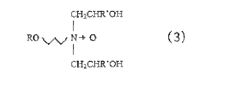
- The electrolytic tin plating solution for chip components according to Claim 1,
wherein the (D) anti-sticking agent is one or more compound selected from a group consisting of aromatic aldehydes and aromatic ketones. - A method of plating chip components, comprising electrolytically tin plating chip components using an electrolytic tin plating solution comprising (A) stannous ions, (B) acid, (C) N,N-dipolyoxyalkylene-N-alkyl amine, an amine oxide, or a blend thereof, and (D) an anti-sticking agent; wherein the pH is 1 or less.
Applications Claiming Priority (1)
| Application Number | Priority Date | Filing Date | Title |
|---|---|---|---|
| JP2008154461A JP5583894B2 (en) | 2008-06-12 | 2008-06-12 | Electrotin plating solution and electrotin plating method |
Publications (3)
| Publication Number | Publication Date |
|---|---|
| EP2141261A2 true EP2141261A2 (en) | 2010-01-06 |
| EP2141261A3 EP2141261A3 (en) | 2010-07-28 |
| EP2141261B1 EP2141261B1 (en) | 2017-03-01 |
Family
ID=41334608
Family Applications (1)
| Application Number | Title | Priority Date | Filing Date |
|---|---|---|---|
| EP09155197.8A Active EP2141261B1 (en) | 2008-06-12 | 2009-03-16 | Electrolytic Tin Plating Solution and Electrolytic Tin Plating Method |
Country Status (6)
| Country | Link |
|---|---|
| US (1) | US20100000873A1 (en) |
| EP (1) | EP2141261B1 (en) |
| JP (1) | JP5583894B2 (en) |
| KR (1) | KR101593475B1 (en) |
| CN (1) | CN101619470B (en) |
| TW (1) | TWI468554B (en) |
Cited By (4)
| Publication number | Priority date | Publication date | Assignee | Title |
|---|---|---|---|---|
| EP2740820A1 (en) | 2012-12-04 | 2014-06-11 | Dr.Ing. Max Schlötter GmbH & Co. KG | Electrolyte and process for the separation of solderable layers |
| WO2019121092A1 (en) | 2017-12-20 | 2019-06-27 | Basf Se | Composition for tin or tin alloy electroplating comprising suppressing agent |
| WO2019201753A1 (en) | 2018-04-20 | 2019-10-24 | Basf Se | Composition for tin or tin alloy electroplating comprising suppressing agent |
| EP3715508A4 (en) * | 2017-10-24 | 2021-10-27 | Mitsubishi Materials Corporation | PLATING LIQUID BASED ON TIN OR A TIN ALLOY |
Families Citing this family (13)
| Publication number | Priority date | Publication date | Assignee | Title |
|---|---|---|---|---|
| CN102308030B (en) | 2009-02-06 | 2015-01-07 | 出分由佳里 | Silver-containing alloy plating bath and electrolytic plating method using the same |
| KR20120051658A (en) * | 2009-07-31 | 2012-05-22 | 신지 데와키 | Tin-containing alloy plating bath, electroplating method using same, and base having electroplated material deposited thereon |
| JP2012021224A (en) * | 2010-06-15 | 2012-02-02 | Mitsubishi Shindoh Co Ltd | Method for preventing sludge generation in tin-plating solution |
| US8888984B2 (en) * | 2012-02-09 | 2014-11-18 | Rohm And Haas Electronic Materials Llc | Plating bath and method |
| JP6133056B2 (en) * | 2012-12-27 | 2017-05-24 | ローム・アンド・ハース電子材料株式会社 | Tin or tin alloy plating solution |
| US20150122662A1 (en) * | 2013-11-05 | 2015-05-07 | Rohm And Haas Electronic Materials Llc | Plating bath and method |
| US20150122661A1 (en) * | 2013-11-05 | 2015-05-07 | Rohm And Haas Electronic Materials Llc | Plating bath and method |
| CN105899714B (en) * | 2013-12-05 | 2018-09-21 | 霍尼韦尔国际公司 | Stannous methanesulfonate solution with pH after the adjustment |
| CN105755513A (en) * | 2016-04-28 | 2016-07-13 | 四川昊吉科技有限公司 | Tinning preservative |
| JP6759736B2 (en) * | 2016-06-10 | 2020-09-23 | 三菱マテリアル株式会社 | Plating liquid |
| JP6818520B2 (en) | 2016-11-11 | 2021-01-20 | ローム・アンド・ハース電子材料株式会社 | Barrel plating or high-speed rotary plating method using neutral tin plating solution |
| US11268203B2 (en) * | 2017-10-24 | 2022-03-08 | Mitsubishi Materials Corporation | Tin or tin alloy plating solution |
| CN109518233B (en) * | 2018-11-27 | 2020-07-14 | 东莞美坚化工原料有限公司 | Conductive solution for preventing miniature electronic component from being stuck on chip and preparation method thereof |
Citations (1)
| Publication number | Priority date | Publication date | Assignee | Title |
|---|---|---|---|---|
| JP2003082492A (en) | 2001-09-13 | 2003-03-19 | Murata Mfg Co Ltd | Method for forming electrode of chip type ceramic electronic parts |
Family Cites Families (14)
| Publication number | Priority date | Publication date | Assignee | Title |
|---|---|---|---|---|
| BE553400A (en) * | 1956-01-16 | |||
| US3616306A (en) * | 1969-11-19 | 1971-10-26 | Conversion Chem Corp | Tin plating bath and method |
| US4000047A (en) * | 1972-11-17 | 1976-12-28 | Lea-Ronal, Inc. | Electrodeposition of tin, lead and tin-lead alloys |
| US4135991A (en) * | 1977-08-12 | 1979-01-23 | R. O. Hull & Company, Inc. | Bath and method for electroplating tin and/or lead |
| US4871429A (en) * | 1981-09-11 | 1989-10-03 | Learonal, Inc | Limiting tin sludge formation in tin or tin/lead electroplating solutions |
| US4717460A (en) * | 1983-12-22 | 1988-01-05 | Learonal, Inc. | Tin lead electroplating solutions |
| US4582576A (en) * | 1985-03-26 | 1986-04-15 | Mcgean-Rohco, Inc. | Plating bath and method for electroplating tin and/or lead |
| US4885064A (en) * | 1989-05-22 | 1989-12-05 | Mcgean-Rohco, Inc. | Additive composition, plating bath and method for electroplating tin and/or lead |
| JP2856857B2 (en) * | 1990-07-27 | 1999-02-10 | 石原薬品株式会社 | Tin, lead or tin-lead alloy plating bath |
| JP2001040498A (en) * | 1999-07-27 | 2001-02-13 | Ne Chemcat Corp | Electronic components coated with tin-copper alloy plating film |
| JP2001234387A (en) * | 2000-02-17 | 2001-08-31 | Yuken Industry Co Ltd | Whisker generation inhibitor and method for preventing tin-based electroplating |
| DE60226196T2 (en) * | 2001-05-24 | 2009-05-14 | Shipley Co., L.L.C., Marlborough | Tin-plating |
| JP4812365B2 (en) * | 2005-08-19 | 2011-11-09 | ローム・アンド・ハース・エレクトロニック・マテリアルズ,エル.エル.シー. | Tin electroplating solution and tin electroplating method |
| WO2007058604A1 (en) * | 2005-11-18 | 2007-05-24 | Replisaurus Technologies Ab | Master electrode and method of forming the master electrode |
-
2008
- 2008-06-12 JP JP2008154461A patent/JP5583894B2/en active Active
-
2009
- 2009-03-16 EP EP09155197.8A patent/EP2141261B1/en active Active
- 2009-06-08 TW TW98119007A patent/TWI468554B/en active
- 2009-06-11 US US12/456,077 patent/US20100000873A1/en not_active Abandoned
- 2009-06-11 KR KR1020090051978A patent/KR101593475B1/en active Active
- 2009-06-12 CN CN2009101462026A patent/CN101619470B/en active Active
Patent Citations (1)
| Publication number | Priority date | Publication date | Assignee | Title |
|---|---|---|---|---|
| JP2003082492A (en) | 2001-09-13 | 2003-03-19 | Murata Mfg Co Ltd | Method for forming electrode of chip type ceramic electronic parts |
Cited By (7)
| Publication number | Priority date | Publication date | Assignee | Title |
|---|---|---|---|---|
| EP2740820A1 (en) | 2012-12-04 | 2014-06-11 | Dr.Ing. Max Schlötter GmbH & Co. KG | Electrolyte and process for the separation of solderable layers |
| EP3715508A4 (en) * | 2017-10-24 | 2021-10-27 | Mitsubishi Materials Corporation | PLATING LIQUID BASED ON TIN OR A TIN ALLOY |
| WO2019121092A1 (en) | 2017-12-20 | 2019-06-27 | Basf Se | Composition for tin or tin alloy electroplating comprising suppressing agent |
| US11459665B2 (en) | 2017-12-20 | 2022-10-04 | Basf Se | Composition for tin or tin alloy electroplating comprising suppressing agent |
| WO2019201753A1 (en) | 2018-04-20 | 2019-10-24 | Basf Se | Composition for tin or tin alloy electroplating comprising suppressing agent |
| US11242606B2 (en) | 2018-04-20 | 2022-02-08 | Basf Se | Composition for tin or tin alloy electroplating comprising suppressing agent |
| US11840771B2 (en) | 2018-04-20 | 2023-12-12 | Basf Se | Composition for tin or tin alloy electroplating comprising suppressing agent |
Also Published As
| Publication number | Publication date |
|---|---|
| EP2141261B1 (en) | 2017-03-01 |
| US20100000873A1 (en) | 2010-01-07 |
| JP5583894B2 (en) | 2014-09-03 |
| JP2009299123A (en) | 2009-12-24 |
| TW201006966A (en) | 2010-02-16 |
| TWI468554B (en) | 2015-01-11 |
| EP2141261A3 (en) | 2010-07-28 |
| CN101619470B (en) | 2012-03-28 |
| KR101593475B1 (en) | 2016-02-12 |
| KR20090129373A (en) | 2009-12-16 |
| CN101619470A (en) | 2010-01-06 |
Similar Documents
| Publication | Publication Date | Title |
|---|---|---|
| EP2141261B1 (en) | Electrolytic Tin Plating Solution and Electrolytic Tin Plating Method | |
| TWI308938B (en) | Pyrophosphoric acid bath for use in copper-tin alloy plating | |
| US20100038254A1 (en) | Tin electroplating solution and tin electroplating method | |
| US7931793B2 (en) | Tin or tin alloy electroplating solution | |
| DE112007000903T5 (en) | Tin electroplating bath, tin-plated coating film, tin electroplating method, and electronic device component | |
| TWI548782B (en) | Cyanide-free acidic matte silver electroplating compositions and methods | |
| KR101712960B1 (en) | Cyanide-free electroplating baths for white bronze based on copper (i) ions | |
| JP5622360B2 (en) | Electrotin plating solution and electrotin plating method | |
| JP4162246B2 (en) | Cyanide-free silver-based plating bath, plated body and plating method | |
| EP3321396B1 (en) | Barrel plating or high-speed rotary plating using a neutral tin plating solution | |
| TW201905242A (en) | Environmentally friendly nickel plating composition and method | |
| TWI623654B (en) | Bismuth electroplating baths and methods of electroplating bismuth on a substrate | |
| CN107502927A (en) | A kind of methanesulfonate tin deposit solution | |
| JP2009191335A (en) | Plating solution and electronic parts | |
| JP2001107287A (en) | Sn-Cu alloy plating bath |
Legal Events
| Date | Code | Title | Description |
|---|---|---|---|
| PUAI | Public reference made under article 153(3) epc to a published international application that has entered the european phase |
Free format text: ORIGINAL CODE: 0009012 |
|
| 17P | Request for examination filed |
Effective date: 20090316 |
|
| AK | Designated contracting states |
Kind code of ref document: A2 Designated state(s): AT BE BG CH CY CZ DE DK EE ES FI FR GB GR HR HU IE IS IT LI LT LU LV MC MK MT NL NO PL PT RO SE SI SK TR |
|
| AX | Request for extension of the european patent |
Extension state: AL BA RS |
|
| PUAL | Search report despatched |
Free format text: ORIGINAL CODE: 0009013 |
|
| AK | Designated contracting states |
Kind code of ref document: A3 Designated state(s): AT BE BG CH CY CZ DE DK EE ES FI FR GB GR HR HU IE IS IT LI LT LU LV MC MK MT NL NO PL PT RO SE SI SK TR |
|
| AX | Request for extension of the european patent |
Extension state: AL BA RS |
|
| RIC1 | Information provided on ipc code assigned before grant |
Ipc: C25D 3/32 20060101ALI20100624BHEP Ipc: C23C 18/54 20060101AFI20091127BHEP |
|
| AKX | Designation fees paid |
Designated state(s): DE FR GB |
|
| 17Q | First examination report despatched |
Effective date: 20160629 |
|
| REG | Reference to a national code |
Ref country code: DE Ref legal event code: R079 Ref document number: 602009044411 Country of ref document: DE Free format text: PREVIOUS MAIN CLASS: C23C0018540000 Ipc: C25D0003300000 |
|
| GRAP | Despatch of communication of intention to grant a patent |
Free format text: ORIGINAL CODE: EPIDOSNIGR1 |
|
| RIC1 | Information provided on ipc code assigned before grant |
Ipc: C25D 7/12 20060101ALN20160919BHEP Ipc: C25D 17/16 20060101ALN20160919BHEP Ipc: C25D 3/30 20060101AFI20160919BHEP |
|
| INTG | Intention to grant announced |
Effective date: 20161019 |
|
| RIN1 | Information on inventor provided before grant (corrected) |
Inventor name: IMANARI, MASAAKI Inventor name: SHIMAZU, MOTOYA Inventor name: OHTA, YASUO Inventor name: TING, FAI LUNG |
|
| GRAS | Grant fee paid |
Free format text: ORIGINAL CODE: EPIDOSNIGR3 |
|
| GRAA | (expected) grant |
Free format text: ORIGINAL CODE: 0009210 |
|
| REG | Reference to a national code |
Ref country code: FR Ref legal event code: PLFP Year of fee payment: 9 |
|
| AK | Designated contracting states |
Kind code of ref document: B1 Designated state(s): DE FR GB |
|
| REG | Reference to a national code |
Ref country code: GB Ref legal event code: FG4D |
|
| REG | Reference to a national code |
Ref country code: DE Ref legal event code: R096 Ref document number: 602009044411 Country of ref document: DE |
|
| REG | Reference to a national code |
Ref country code: DE Ref legal event code: R097 Ref document number: 602009044411 Country of ref document: DE |
|
| PLBE | No opposition filed within time limit |
Free format text: ORIGINAL CODE: 0009261 |
|
| STAA | Information on the status of an ep patent application or granted ep patent |
Free format text: STATUS: NO OPPOSITION FILED WITHIN TIME LIMIT |
|
| 26N | No opposition filed |
Effective date: 20171204 |
|
| REG | Reference to a national code |
Ref country code: FR Ref legal event code: PLFP Year of fee payment: 10 |
|
| GBPC | Gb: european patent ceased through non-payment of renewal fee |
Effective date: 20170601 |
|
| PG25 | Lapsed in a contracting state [announced via postgrant information from national office to epo] |
Ref country code: GB Free format text: LAPSE BECAUSE OF NON-PAYMENT OF DUE FEES Effective date: 20170601 |
|
| P01 | Opt-out of the competence of the unified patent court (upc) registered |
Effective date: 20230530 |
|
| REG | Reference to a national code |
Ref country code: DE Ref legal event code: R082 Ref document number: 602009044411 Country of ref document: DE Representative=s name: ABITZ & PARTNER PATENTANWAELTE MBB, DE Ref country code: DE Ref legal event code: R081 Ref document number: 602009044411 Country of ref document: DE Owner name: DUPONT ELECTRONIC MATERIALS INTERNATIONAL, LLC, US Free format text: FORMER OWNER: ROHM AND HAAS ELECTRONIC MATERIALS LLC, MARLBOROUGH, MASS., US |
|
| PGFP | Annual fee paid to national office [announced via postgrant information from national office to epo] |
Ref country code: DE Payment date: 20260204 Year of fee payment: 18 |
|
| PGFP | Annual fee paid to national office [announced via postgrant information from national office to epo] |
Ref country code: FR Payment date: 20260209 Year of fee payment: 18 |