EP2139130A1 - Communication system - Google Patents
Communication system Download PDFInfo
- Publication number
- EP2139130A1 EP2139130A1 EP08722151A EP08722151A EP2139130A1 EP 2139130 A1 EP2139130 A1 EP 2139130A1 EP 08722151 A EP08722151 A EP 08722151A EP 08722151 A EP08722151 A EP 08722151A EP 2139130 A1 EP2139130 A1 EP 2139130A1
- Authority
- EP
- European Patent Office
- Prior art keywords
- resonance
- electrode
- circuit
- capacitance
- communication system
- Prior art date
- Legal status (The legal status is an assumption and is not a legal conclusion. Google has not performed a legal analysis and makes no representation as to the accuracy of the status listed.)
- Withdrawn
Links
Images





Classifications
-
- H—ELECTRICITY
- H04—ELECTRIC COMMUNICATION TECHNIQUE
- H04B—TRANSMISSION
- H04B13/00—Transmission systems characterised by the medium used for transmission, not provided for in groups H04B3/00 - H04B11/00
-
- H—ELECTRICITY
- H04—ELECTRIC COMMUNICATION TECHNIQUE
- H04B—TRANSMISSION
- H04B13/00—Transmission systems characterised by the medium used for transmission, not provided for in groups H04B3/00 - H04B11/00
- H04B13/005—Transmission systems in which the medium consists of the human body
-
- H—ELECTRICITY
- H04—ELECTRIC COMMUNICATION TECHNIQUE
- H04B—TRANSMISSION
- H04B5/00—Near-field transmission systems, e.g. inductive or capacitive transmission systems
- H04B5/20—Near-field transmission systems, e.g. inductive or capacitive transmission systems characterised by the transmission technique; characterised by the transmission medium
- H04B5/22—Capacitive coupling
-
- H—ELECTRICITY
- H04—ELECTRIC COMMUNICATION TECHNIQUE
- H04B—TRANSMISSION
- H04B5/00—Near-field transmission systems, e.g. inductive or capacitive transmission systems
- H04B5/40—Near-field transmission systems, e.g. inductive or capacitive transmission systems characterised by components specially adapted for near-field transmission
- H04B5/48—Transceivers
Definitions
- the present invention relates to a communication system for transmission/reception via a transmission medium such as a human body.
- a receiver of the aforementioned communication system as disclosed in Patent Document 1 includes a reception electrode for receiving a signal generated from a signal source, and a resonance circuit for extracting the signal at a prescribed frequency.
- the resonance circuit formed of an air-core coil and a chip capacitor has an end of the air-core coil connected to the reception electrode which faces the human body.
- the present invention has been made in consideration of the aforementioned problem, and it is an object of the present invention to provide a communication system which allows the stable communication irrespective of the extended distance between the transmission medium and the reception electrode while preventing the malfunction caused by the noise.
- the communication system is provided with a transmitter for applying a transmission signal to a transmission medium as an electric field, and a receiver for receiving the transmission signal by detecting the electric field via the transmission medium.
- the receiver includes a reception electrode located opposite the transmission medium, a resonance circuit formed of a resonance inductor and a resonance capacitor, and a coupling capacitor for capacitively coupling the reception electrode and the resonance circuit.
- the aforementioned structure is provided with a coupling capacitor for capacitively coupling the reception electrode and the resonance circuit, which ensures the stable communication irrespective of the extended distance between the transmission medium and the reception electrode while preventing the malfunction caused by the noise.
- the coupling capacitor has a capacitance which is equal to or smaller than a value of a capacitance between the receiver and the transmission medium when the receiver moves away from the transmission medium up to a maximum communication distance.
- the structure reduces the coupling capacitance between the receiver and the transmission medium to extend the distance between the transmission medium and the reception electrode, which allows the communication therebetween.
- the coupling capacitor is of variable capacitance type.
- the aforementioned structure is capable of controlling the distance between the transmission medium and the reception electrode, which allows the user to set the communication distance between the transmission medium and the reception electrode by his/her own intention.
- the resonance circuit includes plural resonance inductors capacitively coupled with the reception electrode.
- the aforementioned structure is capable of reducing the frequency shift amount caused by the fluctuation of the distance between the transmission medium and the reception electrode.
- the distance between the transmission medium and the reception electrode may further be extended.
- each of the plural resonance inductors has a switching member, respectively.
- the aforementioned structure is capable of changing the resonance frequency of the resonance circuit.
- the resonance circuit includes the plural resonance capacitor, and each of the resonance inductors and/or the resonance capacitors has a switching member.
- the aforementioned structure allows the resonance circuit to control the inductance and the capacity individually so as to change not only the resonance frequency but also the Q-value.
- the coupling capacitor is formed between a first electrode at the reception electrode side and a second electrode at the resonance circuit side, and at least one of the first electrode and the second electrode is formed on a circuit substrate on which the resonance circuit is formed.
- the aforementioned structure is capable of suppressing the number of components to be used by forming the coupling capacitor on the substrate.
- the coupling capacitor is formed between the first electrode at the reception electrode side and the resonance inductor of the resonance circuit.
- the first electrode at the reception electrode side is formed on the circuit substrate on which the resonance circuit is formed, and the resonance inductor is located at the position opposite the first electrode at the reception side electrode.
- one electrode of the coupling capacitor serves as the resonance inductor. So the coupling capacitor and the resonance inductor may be distribution-constant coupled. As a result, the frequency shift amount may further be reduced, thus extending the communication distance. Furthermore, the aforementioned structure is capable of establishing the distribution-constant coupling between the coupling capacitor and the resonance inductor without increasing the number of components.
- a first wiring at the demodulation unit and a second wiring at a ground side are provided on the circuit substrate, and a capacitance is generated between the first electrode and the first wiring, and the first electrode and the second wiring.
- the first wiring and the second wiring are formed on the substrate such that the capacitance between the first electrode and the first wiring becomes larger than the capacitance between the first electrode and the second wiring.
- the communication system is provided with a transmitter for applying a transmission signal to a transmission medium as an electric field, and a receiver for receiving the transmission signal by detecting the electric field via the transmission medium, wherein the receiver includes a reception electrode located opposite the transmission medium, a resonance circuit formed of a resonance inductor and a resonance capacitor, and a coupling capacitor for capacitively coupling the reception electrode and the resonance circuit.
- the structure ensures the stable communication irrespective of the extended distance between the transmission medium and the reception electrode while preventing malfunction caused by the noise.
- Patent Document 1 The inventor has been trying to solve the technical problems disclosed in Patent Document 1, that is, the communication is disabled by the extended distance between the transmission medium and the reception electrode, and malfunction is caused by the noise.
- the inventor also found that when the resonance feature of the resonance circuit is broadened to make the Q-value small to prevent the large change in the gain irrespective of the shift of the resonance frequency, the malfunction occurs under the influence of the noise close to the frequency of the carrier wave of the transmission signal.
- the inventor invented the communication system which employs the coupling capacitor for capacitively coupling the reception electrode and the resonance circuit to establish the stable communication irrespective of the extended distance between the transmission medium and the reception electrode while preventing the malfunction caused by the noise.
- the present invention provides a communication system which includes a transmitter for applying a transmission signal to a transmission medium as the electric field, and a receiver for receiving the transmission signal by detecting the electric field via the transmission medium.
- the receiver includes a reception electrode opposite the transmission medium, a resonance circuit formed of a resonance inductor and a resonance capacitor, and a coupling capacitor for capacitively coupling the reception electrode and the resonance circuit for the stable communication irrespective of the extended distance between the transmission medium and the reception electrode while preventing the malfunction caused by the noise.
- Fig. 1(a) is a view schematically showing a structure of a part of a communication system at a receiver side according to an example of the present invention.
- Fig. 1(b) is a view showing an equivalent circuit as a part of the communication system at the receiver side shown in Fig. 1(a) .
- the communication system shown in Fig. 1 is mainly formed of a transmission medium such as a human body 1 for transmitting a transmission signal via the electric field, a transmitter (not shown) for applying the transmission signal having an information signal modulated to the transmission medium as the electric field, and a receiver 2 for detecting the transmission signal indicating the electric field change via the transmission medium to demodulate the electric field change into the information signal.
- the transmitter and the transmission medium (human body 1), and the receiver 2 and the transmission medium (human body 1) are capacitively coupled electrically via a capacitor (capacity Cx between the receiver 2 and the transmission medium 1) such that the modulated transmission signal is transmitted to the transmission medium as the electric field.
- the transmission medium allows the displacement current to flow, but does not allow the stationary current to flow, requiring no need of electric continuity.
- the transmitter and the transmission medium may be capacitively coupled via the thin cloth, which makes it possible to transmit the transmission signal.
- the transmitter applies the modulated transmission signal to the transmission medium as the electric field.
- the transmitter includes a modulation circuit for modulating the information signal with the carrier, and a conversion circuit for amplifying the modulated signal into the transmission signal so as to be converted into the signal indicating the voltage change.
- modulation methods such as FM, AM, FSK, ASK, and PSK may be employed.
- the receiver 2 detects the change in the electric field via the transmission medium to obtain the demodulated signal corresponding to the transmission signal.
- the receiver 2 located opposite the transmission medium includes a reception electrode 21 which receives the electric field from the transmission medium, a resonance circuit 22 formed of a resonance inductor 22a (inductance: Lo) and a resonance capacitor 22b (capacity: Co), and a coupling capacitor 23 (capacity: Cc) for capacitively coupling the reception electrode 21 and the resonance circuit 22.
- the rear stage of the resonance circuit 22 is connected to a detection circuit (not shown) for detecting the amplified electric field, and a demodulation circuit (not shown) for demodulating the transmission signal using the detected physical quantity.
- the coupling capacitor 23 suppresses the shift of the resonance frequency of the resonance circuit 22, which is caused by the change in the capacitance between the transmission medium and the reception electrode 21 opposite the transmission medium.
- the coupling capacitor 23 has the capacitance equal to or smaller than the capacitance value between the receiver 2 and the human body 1 when the receiver 2 moves away from the human body 1 up to the maximum communication distance. This makes it possible to make the coupling capacity between the receiver 2 and the human body 1 small, thus extending the communication distance between the transmission medium and the reception electrode.
- the coupling capacitor 23 is of variable capacity type. This makes it possible to control the distance between the receiver 2 and the human body 1, or the distance between the transmission medium and the reception electrode. As a result, the user is capable of setting the communication distance between the transmission medium and the reception electrode arbitrarily or automatically in accordance with the environment for the use of the transmitter/receiver.
- the information signal is modulated with the carrier at the frequency (several tens kHz to several MHz) indicating the conductivity by the transmitter for providing the modulated signal to the human body 1.
- the modulated signal is then amplified and converted into the voltage change signal.
- the voltage change is added to the electrode of the transmitter to generate the electric field corresponding to the modulated signal around the electrode.
- the resultant electric field is applied to the human body 1 as the transmission signal.
- the electric field (transmission signal) applied to the human body 1 is received by the reception electrode 21 of the receiver 2.
- the resonance circuit 22 and the detection circuit (not shown) at the rear stage thereof detect the modulated signal.
- a demodulation circuit located at the rear stage of the detection circuit demodulates the signal with the carrier used in the transmitter to provide the information signal so as to be transmitted/received via the human body as the transmission medium.
- an LC parallel resonance circuit (half bandwidth is approximately ⁇ 0.3 MHz) has the resonance frequency of the resonance circuit 22 adjusted to 10 MHz in the state where the capacitance Cx between the human body 1 and the reception electrode 21 is 10 pF (assumed to be in the normal state).
- the capacitance Cx is decreased to reach the value at which the output amplitude at 10 MHz becomes half the value in the normal state, and such value is set to the allowable capacitance Cx.
- the relationship between the allowable capacitance Cx and the coupling capacitor Cc is shown in Fig. 2 .
- the allowable capacitance Cx is 9.45 pF which allows the Cx fluctuation by only approximately 5% from the value of 10 pF in the normal state where the resonance frequency of the resonance circuit is adjusted. Supposing that the electrode area is set to 12 cm 2 (4cm x 3 cm), the Cx of 10 pF corresponds to the gap of 1mm between the human body and the reception electrode. Accordingly, the allowable capacitance Cx of 9.45 pF corresponds to the gap of 1.12 mm, which allows the fluctuation of only 0.12 mm (120 ⁇ m) as the gap difference for enabling the communication. In the circuit disclosed in Patent Document 1, the communication will be disabled if the gap becomes equal to or larger than 1.12 mm. The use of such circuit in the communication system according to the present invention may make the communication unstable.
- the allowable capacitance Cx becomes 1.5 pF when the value of the coupling capacitor Cc 23 is 1 pF, which allows the fluctuation up to 1/6 of the value of 10 pF in the normal state.
- the allowable capacitance Cx of 1.5 pF corresponds to the gap of approximately 7 mm supposing that the electrode area is 12 cm 2 (4 cm x 3 cm).
- the allowable capacitance Cx is 0.4 pF when the value of the coupling capacitor Cc 23 is 0.3 pF, which corresponds to the gap of approximately 26mm supposing that the electrode area is 12 cm 2 (4 cm x 3 cm).
- the aforementioned values are obtained by the adjustment on the assumption that the Cx value is equal to 10 pF.
- the Cx value in the normal state may be changed to adjust the communication distance.
- the resonance frequency shift suppressing effect in the receiver of the communication system according to the present invention will be described.
- the circuit shown in Fig. 1(b) is used for the simulation, and the result is shown in Fig. 3 .
- the frequency of the AC power source 24 was set to 10 MHz
- the amplitude was set to 1 Vpp
- the capacity of the coupling capacitor Cc 23 was set to 10 pF
- the inductance of the resonance inductor in the resonance circuit 23 was set to 22 ⁇ H, respectively.
- the capacitance Cx between the human body 1 and the reception electrode 21 is set to 10 pF in the normal state
- the capacity of the resonance capacitor is set to 6.5 pF such that the resonance frequency becomes 10 MHz.
- the circuit which is not provided with the coupling capacitor was subjected to the simulation, and the results are shown in Fig. 3 as the comparative example.
- the frequency of the AC power source 24 was set to 10 MHz
- the amplitude was set to 1 Vpp
- the inductance of the resonance inductor in the resonance circuit 23 was set to 22 ⁇ H, respectively.
- the capacitance Cx between the human body 1 and the reception electrode 21 is set to 10 pF in the normal state
- the capacity of the resonance capacitor set to 1.5 pF such that the resonance frequency becomes 10 MHz.
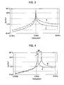
- Fig. 4 shows each resonance frequency shift with the capacitance Cx set to 5 pF (gap larger than the one in the normal state) in both of the circuit according to the example and the circuit as the comparative example.
- the circuit according to the example (characteristic curve A) suppresses the frequency shift SA to 10.8 MHz (8%).
- the circuit as the comparative example (characteristic curve B) has the frequency shift SB as large as 13.3 MHz (33%).
- FIG. 5 shows each resonance frequency shift with the capacitance Cx set to 20 pF (gap smaller than the one in the normal state) in both of the circuit according to the example and the circuit as the comparative example.
- the circuit according to the example (characteristic curve A) suppresses the frequency shift SA to 9.3 MHz (-7%).
- the circuit as the comparative example has the frequency shift SB as large as 7.3 MHz (-27%).
- the circuit shown in Fig. 1(b) has the resonance circuit 22 formed as the parallel resonance circuit.
- the coupling capacitor 23 may suppress the resonance frequency shift as well.
- the output change caused by the fluctuation in the capacitance Cx between the human body 1 and the reception electrode 21 was studied with respect to the circuit shown in Fig. 1(b) .
- the results are shown in Figs. 7 to 9 .
- the circuit shown in Fig. 1(b) provided with no coupling capacitor was subjected to the simulation.
- the simulation result is shown in Fig. 6 .
- the frequency of the AC power source 24 was set to 10 MHz, and the amplitude was set to 1 Vpp.
- Fig. 6 shows the frequency characteristic of the circuit provided with no coupling capacitor as the comparative example having the allowable Cx set to 9.45 pF.
- the frequency reaches the peak value of 10.0 MHz with the capacitance Cx of 10 pF, and the output at the frequency of 10 MHz is 30 V.
- the frequency reaches the peak value of 10.14 MHz with the capacitance Cx of 9.7 pF, and the output at the frequency of 10 MHz is 21.7 V.
- the frequency reaches the peak value of 10.3 MHz with the capacitance Cx of 9.45 pF, and the output at the frequency of 10 MHz is 14.8 V.
- the frequency reaches the peak value of 10.4 MHz with the capacitance Cx of 9.1 pF, and the output at the frequency of 10 MHz is 9.5 V.
- An output difference D1 between the case with the capacitance Cx of 10 pF and the case with the capacitance Cx of 9.1 pF is 20.5 V.
- the output at the frequency of 10 MHz becomes half the value in the normal state when the capacitance Cx is 9.45 pF. Accordingly, the allowable Cx value is 9.45 pF.
- Fig. 7 shows the frequency characteristics of the circuit according to the example when the capacity of the coupling capacitor Cc is set to 30 pF, and the allowable Cx is set to 9.1 pF.
- the frequency reaches the peak value of 10.0 MHz with the capacitance Cx of 10 pF, and the output at the frequency of 10 MHz is 22.5 V.
- the frequency reaches the peak value of 10. 13 MHz with the capacitance Cx of 9.5 pF, and the output at the frequency of 10 MHz is 16.5 V.
- the frequency reaches the peak value of 10.23 MHz with the capacitance Cx of 9.1 pF, and the output at the frequency of 10 MHz is 11.3 V.
- the frequency reaches the peak value of 10.35 MHz with the capacitance Cx of 8.7 pF, and the output at the frequency of 10 MHz is 8.2 V.
- An output difference D2 between the case with the capacitance Cx of 10 pF and the case with the capacitance of Cx of 8.7 pF is 14.3 V.
- the output at the frequency of 10 MHz becomes half the value in the normal state when the capacitance Cx is 9.1 pF. Accordingly, the allowable capacitance Cx is 9.1 pF.
- the change in the output caused by the gap between the human body and the reception electrode is small. In other words, the width of the gap which provides the output for enabling the communication may be extended.
- the circuit of the example is capable of performing the stable communication in spite of the extended distance between the transmission medium and the reception electrode.
- Fig. 8 shows the frequency characteristic of the circuit according to the example having the capacity of the coupling capacitor Cc set to 3pF, and the allowable capacitance Cx set to 5.0 pF.
- the frequency reaches the peak value of 10.0 MHz with the capacitance Cx of 10 pF, and the output at the frequency of 10 MHz is 6.93 V.
- the frequency reaches the peak value of 10.09 MHz with the capacitance Cx of 7.0 pF, and the output at the frequency of 10 MHz is 5.42V.
- the frequency reaches the peak value of 10.20 MHz with the capacitance Cx of 5.0 pF, and the output at the frequency of 10 MHz is 3.48 V.
- the frequency reaches the peak value of 10.27 MHz with the capacitance Cx of 4.0 pF, and the output at the frequency of 10 MHz is 2.55 V.
- An output difference D3 between the case with the capacitance Cx of 10 pF and the case with the capacitance Cx of 4.0 pF is 4.38 V.
- Fig. 9 shows the frequency characteristic of the circuit according to the example having the capacity of the coupling capacitor Cc set to 1 pF, and the allowable capacitance Cx set to 1.5 pF.
- the frequency reaches the peak value of 10.0 MHz with the capacitance Cx of 10 pF, and the output at the frequency of 10 MHz is 2.7 V.
- the frequency reaches the peak value of 10.07 with the capacitance Cx of 3.0 pF, and the output at the frequency of 10 MHz is 2.1 V.
- the frequency reaches the peak value of 10.14 MHz with the capacitance Cx of 1.5 pF, and the output at the frequency of 10 MHz is 1.34 V.
- the frequency reaches the peak value of 10.19 MHz with the capacitance Cx of 1.0 pF, and the output at the frequency of 10 MHz is 0.96 V.
- An output difference D4 between the case with the capacitance Cx of 10 pF and the case with the capacitance Cx of 1.0 pF is 1.74 V.
- the output at the frequency of 10 MHz becomes half the value in the normal state when the capacitance Cx is 1.5 pF, and accordingly the allowable capacitance Cx is 1.5 pF.
- the resonance circuit 22 shown in Fig. 1(b) is formed of one resonance inductor 22a and one resonance capacitor 22b.
- the present invention is not limited to the aforementioned structure.
- the resonance circuit 22 may include plural resonance inductors capacitively coupled with the reception electrode 21. This makes it possible to further reduce the frequency shift amount caused by fluctuation of the distance between the transmission medium and the reception electrode, thus extending the distance therebetween.
- the division number of the resonance inductor is not limited.
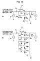
- Fig. 10(a) represents the case where the resonance inductor is divided into two parts.
- the resonance inductor of the resonance circuit is formed of two resonance inductors 21a1 and 22a1 each with inductance of 11 ⁇ H connected in series (two-part type).
- the coupling capacitor 23 is divided into two coupling capacitors 23a, 23a each with the capacity of 5 pF connected in parallel so as to be connected to the resonance inductor.
- the capacity of the resonance capacitor is set to 8.1 pF such that the resonance frequency becomes 10 MHz in the normal state where the Cx is set to 10 pF.
- the resonance inductor is divided into five parts (five-part type).
- the coupling capacitor 23 is formed of five coupling capacitors 23b, 23b, 23b, 23b, 23b each with the capacity of 2 pF connected in parallel
- the resonance inductor is formed of five resonance inductors 22a2, 22a2, 22a2, 22a2, 22a2, 22a2 each with the inductance of 4.4 ⁇ H connected in series.
- the capacity of the resonance capacitor is set to 8.9 pF such that the resonance frequency becomes 10 MHz in the normal state where Cx is set to 10 pF.
- the simulation is conducted with respect to the effect of dividing the resonance inductor, and the results are shown in Figs. 11 (a) to 11(c) .
- the frequency of the AC power source 24 was set to 10 MHz, and the amplitude was set to 1 Vpp.
- Fig. 11 (b) Each resonance frequency shift in the aforementioned three circuits when the capacitance Cx is set to 1 pF (gap larger than the one in the normal state) is shown in Fig. 11 (b) .
- Fig. 11 (b) the larger the division number of the resonance inductor becomes, the less the frequency shift is suppressed.
- the resonance frequency shift when the capacitance Cx is set to 100 pF (gap smaller than the one in the normal state) is shown in Fig. 11(c) .
- Fig. 11 (c) the larger the division number of the resonance inductors becomes, the less the frequency shift is suppressed.
- the resonance circuit 22 may be structured such that each of the plural resonance inductors is provided with a selector switch 25 for allowing the resonance frequency in the resonance circuit 22 to be changed.
- the resonance circuit 22 may be structured to divide the resonance capacitor 22b into plural capacitors 22b1, and to provide selector switches 25, 26 for the resonance inductor and/or the resonance capacitor as shown in Fig. 12(b) .
- the resonance circuit 22 is capable of controlling the inductance and the capacity separately so as to change not only the resonance frequency but also the Q-value independently. For example, the inductance of the resonance inductor is increased to make the Q-value large while maintaining the same resonance frequency. Conversely, the capacity of the resonance capacitor is increased to make the Q-value small. Specifically, if the noise is required to be eliminated, the Q-value is made larger. If the communication speed is accelerated by increasing the band, the Q-value is made smaller.
- FIG. 12(b) is capable of executing the aforementioned control.
- Each of the structures shown in Figs. 12(a) and 12(b) provides the switch for each resonance inductor or the resonance capacitor.
- only one switch may be provided with respect to at least two units of the resonance inductors or the resonance capacitors.
- Fig. 13 shows a structure of the receiver in the communication system according to the example of the present invention.
- Fig. 13(a) shows a pattern on the substrate.
- Fig. 13(b) is a view showing an electronic element mounted on the pattern.
- Fig. 13(c) is a sectional view taken along line XIIC-XIIC of Fig. 13(a) .
- patterns 32a, 32b for the coupling capacitor Cc and patterns 33a, 33b for the resonance circuit are formed on a circuit substrate 31.
- the pattern 32a for the coupling capacitor Cc corresponds to the resonance circuit side electrode (second electrode), and the pattern 32b corresponds to the receiver side electrode (first electrode).
- the pattern 33a for the resonance circuit corresponds to the one at the demodulation circuit side, and the pattern 33b corresponds to the one at the ground side.
- the coupling capacitor Cc is formed between the receiver side electrode 32b and the resonance circuit side electrode 32a, one of which (in this case, the resonance circuit side electrode 32a) is formed on the circuit substrate 31. In this way, the coupling capacitor Cc is built in the circuit substrate 31.
- the receiver side electrode 32b is connected to the reception electrode
- the demodulation circuit side pattern 33a is connected to the demodulation circuit
- the ground side pattern 33b is connected to the ground.
- Fig. 13(b) shows the state where a resonance inductor 34 and a resonance capacitor 35 are mounted on the patterns as shown in Fig. 13(a) . That is, the resonance inductor 34 is mounted on the demodulation circuit side pattern 33a and the ground side pattern 33b connected to the resonance circuit side electrode 32a. The resonance capacitor 35 is mounted on the demodulation circuit side pattern 33a and the ground side pattern 33b, which are not connected to the resonance circuit side electrode 32a.
- the resonance circuit 22 is formed of the thus connected resonance inductor 34 and the resonance capacitor 35. Respective locations of the resonance inductor 34 and the resonance capacitor 35 may be switched therebetween.
- the component for the resonance circuit is mostly required to have the fine adjustment function for adjusting the resonance frequency.
- the trimmer capacitor is used for the resonance capacitor in most of the case. Accordingly, it is not suitable for the element to be formed in the substrate.
- the coupling capacitor Cc is capable of determining the capacity value by setting the communication distance, it is suitable for the element to be formed on the substrate.
- the coupling capacitor Cc with the structure shown in Fig. 13 is employed to stabilize the resonance frequency and to reduce the number of components. In the structure having the coupling capacitor Cc built in the circuit substrate 31, the number of the components may further be reduced by forming the resonance circuit in the integrated circuit such as the modulation circuit.
- the receiver side electrode 32b of the coupling capacitor Cc is formed on the circuit substrate 31, and the demodulation circuit side pattern 33a and the ground side pattern 33b are formed at both sides of the electrode 32b.
- the resonance inductor 34 and the resonance capacitor 35 are mounted on the demodulation circuit side pattern 33a and the ground side pattern 33b, respectively to form the resonance circuit 22.
- the resonance inductor 34 is located to face the receiver side electrode 32b such that the coupling capacitor Cc is formed between the receiver side electrode 32b and the resonance inductor 34 of the resonance circuit 22.
- the wiring in the resonance inductor 34 and the receiver side electrode 32b formed on the circuit substrate 31 are capacitively coupled to establish the distribution-constant coupling as shown in Fig. 10 .
- This may provide the effect for further stabilizing the resonance frequency.
- the frequency shift amount is reduced so as to extend the communication distance.
- the aforementioned structure eliminates the resonance circuit side electrode 32a, thus establishing the distribution constant coupling without increasing the number of components to be employed.
- the material with high dielectric constant such as resin is filled between the circuit substrate 31 and the resonance inductor 34 so as to intensify the electrostatic coupling between the receiver side electrode 32b and the resonance inductor 34 as the resonance circuit side electrode.
- the adhesive agent may be employed as the material filled between the receiver side electrode 32b and the resonance inductor 34 so as to be adhered with each other.
- the resonance circuit side electrode is allowed to serve as the resonance inductor in the integrated circuit, thus establishing the distribution-constant coupling to provide the similar effect.
- the wiring of the resonance inductor 34 may be structured as shown in Figs. 15(a) to 15(c) .
- the distribution-constant coupling is established between the receiver side electrode 32b and the wiring in the resonance inductor 34 to provide the effect for stabilizing the resonance frequency.
- the receiver side resonance electrode 32b may be formed on the surface of the resonance inductor 34 as shown in Figs. 15(d) to 15(f) rather than being formed on the circuit substrate 31 to establish the distribution-constant coupling between the receiver side electrode 32b and the wiring in the resonance inductor 34, thus providing the similar effect.
- the receiver side electrode 32b may be formed on the surface of the resonance inductor 34 as shown in Figs. 15(d) to 15(f) so as to be mounted while being directed upward or sideways. This makes it possible to subject the receiver side electrode 32b to the wire bonding and the ball bonding.
- the capacitance is generated between the resonance circuit side electrode and a demodulation circuit side wiring 36 connected to the demodulation circuit, and between the resonance circuit side electrode and a ground side wiring 37 connected to the ground of the demodulation circuit, respectively as shown in Fig. 16(a) .
- the capacitance between the demodulation circuit side wiring 36 and the receiver side electrode 32b is designated as Cc'
- the capacitance between the ground side wiring 37 and the receiver side electrode 32b is designated as Cg
- the equivalent circuit in the aforementioned structure is represented as shown in Fig. 17 .
- the demodulation circuit side wiring 36 and the ground side wiring 37 are formed on the circuit substrate 31 such that the capacitance Cc' becomes larger than the capacitance Cg.
- the region of the ground side wiring 37, which is adjacent to the receiver side electrode 32b is made small, and in the structure shown in Fig. 16(c) , the distance between the receiver side electrode 32b and the ground side wiring 37 is made larger than the distance between the receiver side electrode 32b and the demodulation circuit side wiring 36.
- the demodulation circuit side wiring 36 may be connected to an inter-layer wiring 38 via a through hole 39 so as to increase the capacitance between the demodulation circuit side wiring 36 and the receiver side electrode 32b using the inter-layer capacity.
- the use of the aforementioned structure may suppress the signal from the reception side electrode 32b from being drawn into the ground, thus providing improved sensitivity.
- the demodulation circuit side wiring 36 and the ground side wiring 37 are formed such that the capacitance Cc' becomes larger than the capacitance Cg, thus providing the similar effect.
- the present invention is not limited to the aforementioned examples, but may be formed into various structures.
- the modulation circuit and the conversion circuit in the transmitter, and the detection circuit and the demodulation circuit in the receiver are not limited to those described in the examples and may be modified into various forms, respectively.
- the dimension and values in the examples are not limited but may be changed so as not to deviate from the scope of the present invention.
- the structure may be arbitrarily changed so long as it does not deviate from the scope of the present invention.
Landscapes
- Engineering & Computer Science (AREA)
- Computer Networks & Wireless Communication (AREA)
- Signal Processing (AREA)
- Near-Field Transmission Systems (AREA)
- Filters And Equalizers (AREA)
Abstract
Description
- The present invention relates to a communication system for transmission/reception via a transmission medium such as a human body.
- Accompanied with the recent technical development, the totally new communication method using the electric field guided to a transmission medium such as the human body has been proposed. A receiver of the aforementioned communication system as disclosed in
Patent Document 1 includes a reception electrode for receiving a signal generated from a signal source, and a resonance circuit for extracting the signal at a prescribed frequency. The resonance circuit formed of an air-core coil and a chip capacitor has an end of the air-core coil connected to the reception electrode which faces the human body. - Patent Document 1: Japanese Unexamined Patent Application Publication No.
2005-94466 - In the communication system disclosed in
Patent Document 1, if the distance between the human body and the reception electrode of the receiver extends by a very small amount, the communication will be disabled or interfered owing to the noise close to the carrier frequency of the communication (for example, the noise generated by the mobile phone). - The present invention has been made in consideration of the aforementioned problem, and it is an object of the present invention to provide a communication system which allows the stable communication irrespective of the extended distance between the transmission medium and the reception electrode while preventing the malfunction caused by the noise.
- The communication system according to the present invention is provided with a transmitter for applying a transmission signal to a transmission medium as an electric field, and a receiver for receiving the transmission signal by detecting the electric field via the transmission medium. The receiver includes a reception electrode located opposite the transmission medium, a resonance circuit formed of a resonance inductor and a resonance capacitor, and a coupling capacitor for capacitively coupling the reception electrode and the resonance circuit.
- The aforementioned structure is provided with a coupling capacitor for capacitively coupling the reception electrode and the resonance circuit, which ensures the stable communication irrespective of the extended distance between the transmission medium and the reception electrode while preventing the malfunction caused by the noise.
- In the communication system according to the present invention, preferably, the coupling capacitor has a capacitance which is equal to or smaller than a value of a capacitance between the receiver and the transmission medium when the receiver moves away from the transmission medium up to a maximum communication distance. The structure reduces the coupling capacitance between the receiver and the transmission medium to extend the distance between the transmission medium and the reception electrode, which allows the communication therebetween.
- In the communication system according to the present invention, preferably, the coupling capacitor is of variable capacitance type. The aforementioned structure is capable of controlling the distance between the transmission medium and the reception electrode, which allows the user to set the communication distance between the transmission medium and the reception electrode by his/her own intention.
- In the communication system according to the present invention, preferably, the resonance circuit includes plural resonance inductors capacitively coupled with the reception electrode. The aforementioned structure is capable of reducing the frequency shift amount caused by the fluctuation of the distance between the transmission medium and the reception electrode. The distance between the transmission medium and the reception electrode may further be extended.
- In the communication system according to the present invention, preferably, each of the plural resonance inductors has a switching member, respectively. The aforementioned structure is capable of changing the resonance frequency of the resonance circuit.
- In the communication system according to the present invention, preferably, the resonance circuit includes the plural resonance capacitor, and each of the resonance inductors and/or the resonance capacitors has a switching member. The aforementioned structure allows the resonance circuit to control the inductance and the capacity individually so as to change not only the resonance frequency but also the Q-value.
- In the communication system according to the present invention, preferably, the coupling capacitor is formed between a first electrode at the reception electrode side and a second electrode at the resonance circuit side, and at least one of the first electrode and the second electrode is formed on a circuit substrate on which the resonance circuit is formed.
- The aforementioned structure is capable of suppressing the number of components to be used by forming the coupling capacitor on the substrate.
- In the communication system according to the present invention, preferably, the coupling capacitor is formed between the first electrode at the reception electrode side and the resonance inductor of the resonance circuit. Preferably, the first electrode at the reception electrode side is formed on the circuit substrate on which the resonance circuit is formed, and the resonance inductor is located at the position opposite the first electrode at the reception side electrode.
- In the structure, one electrode of the coupling capacitor serves as the resonance inductor. So the coupling capacitor and the resonance inductor may be distribution-constant coupled. As a result, the frequency shift amount may further be reduced, thus extending the communication distance. Furthermore, the aforementioned structure is capable of establishing the distribution-constant coupling between the coupling capacitor and the resonance inductor without increasing the number of components.
- In the communication system according to the present invention, preferably, a first wiring at the demodulation unit and a second wiring at a ground side are provided on the circuit substrate, and a capacitance is generated between the first electrode and the first wiring, and the first electrode and the second wiring. The first wiring and the second wiring are formed on the substrate such that the capacitance between the first electrode and the first wiring becomes larger than the capacitance between the first electrode and the second wiring. The aforementioned structure prevents the signal from the reception electrode from being drawn into the ground, resulting in the improved sensitivity.
- The communication system according to the present invention is provided with a transmitter for applying a transmission signal to a transmission medium as an electric field, and a receiver for receiving the transmission signal by detecting the electric field via the transmission medium, wherein the receiver includes a reception electrode located opposite the transmission medium, a resonance circuit formed of a resonance inductor and a resonance capacitor, and a coupling capacitor for capacitively coupling the reception electrode and the resonance circuit. The structure ensures the stable communication irrespective of the extended distance between the transmission medium and the reception electrode while preventing malfunction caused by the noise.
-
- [
Fig. 1] Fig. 1(a) is a view schematically showing a part of a communication system at a receiver side according to an example of the present invention. -
Fig. 1(b) is a view showing an equivalent circuit as a part of the communication system at the receiver side shown inFig. 1(a) . - [
Fig. 2] Fig. 2 is a view showing a relationship between the allowable Cx and a capacity Cc of the coupling capacitor. - [
Fig. 3] Fig. 3 is a view showing the shift of the resonance frequency in the receiver. - [
Fig. 4] Fig. 4 is a view showing the shift of the resonance frequency in the receiver. - [
Fig. 5] Fig. 5 is a view showing the shift of the resonance frequency in the receiver. - [
Fig. 6] Fig. 6 is a view showing an output change caused by the fluctuation in the capacitance Cx of the receiver. - [
Fig. 7] Fig. 7 is a view showing the output change caused by the fluctuation in the capacitance Cx of the receiver. - [
Fig. 8] Fig. 8 is a view showing the output change caused by the fluctuation in the capacitance Cx of the receiver. - [
Fig. 9] Fig. 9 is a view showing the output change caused by the fluctuation in the capacitance Cx of the receiver. - [
Fig. 10] Figs. 10(a) and 10(b) are views each showing another example of an equivalent circuit as a part of the communication system at the receiver side. - [
Fig. 11] Figs. 11(a) to 11(c) are views each showing the shift of the resonance frequency of the receiver. - [
Fig. 12] Figs. 12(a) and 12(b) are views each showing another example of the equivalent circuit as a part of the communication system at the receiver side. - [
Fig. 13] Fig. 13 shows a structure of the receiver in the communication system according to the example of the present invention, whereinFig. 13(a) is a view showing a pattern on the circuit substrate;Fig. 13(b) is a view showing the state where the electronic element is mounted on the pattern; andFig. 13(c) is a sectional view taken along line XIIC-XIIC shown inFig. 13(a) . - [
Fig. 14] Fig. 14 shows a structure of the receiver in the communication system according to the example of the present invention, whereinFig. 14(a) is a view showing the pattern on the circuit substrate; andFig. 14(b) is a view showing the state where the electronic element is mounted on the pattern. - [
Fig. 15] Figs. 15(a) to 15(f) are views each showing an example of the resonance inductor used for the receiver. - [
Fig. 16] Figs. 16(a) to 16(d) are views each showing a pattern on the circuit substrate of the receiver in the communication system according to the example of the present invention, andFig. 16(e) is a sectional view taken along line XVE-XVE ofFig. 16(d) . - [
Fig. 17] Fig. 17 shows a diagram of the equivalent circuit of the receiver with the pattern shown inFig. 16 . - The inventor has been trying to solve the technical problems disclosed in
Patent Document 1, that is, the communication is disabled by the extended distance between the transmission medium and the reception electrode, and malfunction is caused by the noise. The inventor found that the shift of the resonance frequency of the resonance circuit in the receiver, which is caused by the change in the capacitance between the transmission medium and the reception electrode of the receiver opposite the transmission medium disables the communication resulting from the extended distance between the transmission medium and the reception electrode. The inventor also found that when the resonance feature of the resonance circuit is broadened to make the Q-value small to prevent the large change in the gain irrespective of the shift of the resonance frequency, the malfunction occurs under the influence of the noise close to the frequency of the carrier wave of the transmission signal. In view of the aforementioned findings, the inventor invented the communication system which employs the coupling capacitor for capacitively coupling the reception electrode and the resonance circuit to establish the stable communication irrespective of the extended distance between the transmission medium and the reception electrode while preventing the malfunction caused by the noise. - The present invention provides a communication system which includes a transmitter for applying a transmission signal to a transmission medium as the electric field, and a receiver for receiving the transmission signal by detecting the electric field via the transmission medium. In the communication system, the receiver includes a reception electrode opposite the transmission medium, a resonance circuit formed of a resonance inductor and a resonance capacitor, and a coupling capacitor for capacitively coupling the reception electrode and the resonance circuit for the stable communication irrespective of the extended distance between the transmission medium and the reception electrode while preventing the malfunction caused by the noise.
- An example according to the present invention will be described in detail referring to the accompanying drawings.
-
Fig. 1(a) is a view schematically showing a structure of a part of a communication system at a receiver side according to an example of the present invention.Fig. 1(b) is a view showing an equivalent circuit as a part of the communication system at the receiver side shown inFig. 1(a) . The communication system shown inFig. 1 is mainly formed of a transmission medium such as ahuman body 1 for transmitting a transmission signal via the electric field, a transmitter (not shown) for applying the transmission signal having an information signal modulated to the transmission medium as the electric field, and areceiver 2 for detecting the transmission signal indicating the electric field change via the transmission medium to demodulate the electric field change into the information signal. - In the communication system, the transmitter and the transmission medium (human body 1), and the
receiver 2 and the transmission medium (human body 1) are capacitively coupled electrically via a capacitor (capacity Cx between thereceiver 2 and the transmission medium 1) such that the modulated transmission signal is transmitted to the transmission medium as the electric field. In the aforementioned case, the transmission medium allows the displacement current to flow, but does not allow the stationary current to flow, requiring no need of electric continuity. In the case where the transmitter is kept in the pocket, the transmitter and the transmission medium may be capacitively coupled via the thin cloth, which makes it possible to transmit the transmission signal. - The transmitter applies the modulated transmission signal to the transmission medium as the electric field. The transmitter includes a modulation circuit for modulating the information signal with the carrier, and a conversion circuit for amplifying the modulated signal into the transmission signal so as to be converted into the signal indicating the voltage change. Various modulation methods such as FM, AM, FSK, ASK, and PSK may be employed.
- The
receiver 2 detects the change in the electric field via the transmission medium to obtain the demodulated signal corresponding to the transmission signal. Thereceiver 2 located opposite the transmission medium includes areception electrode 21 which receives the electric field from the transmission medium, aresonance circuit 22 formed of aresonance inductor 22a (inductance: Lo) and aresonance capacitor 22b (capacity: Co), and a coupling capacitor 23 (capacity: Cc) for capacitively coupling thereception electrode 21 and theresonance circuit 22. The rear stage of theresonance circuit 22 is connected to a detection circuit (not shown) for detecting the amplified electric field, and a demodulation circuit (not shown) for demodulating the transmission signal using the detected physical quantity. - The
coupling capacitor 23 suppresses the shift of the resonance frequency of theresonance circuit 22, which is caused by the change in the capacitance between the transmission medium and thereception electrode 21 opposite the transmission medium. Preferably, thecoupling capacitor 23 has the capacitance equal to or smaller than the capacitance value between thereceiver 2 and thehuman body 1 when thereceiver 2 moves away from thehuman body 1 up to the maximum communication distance. This makes it possible to make the coupling capacity between thereceiver 2 and thehuman body 1 small, thus extending the communication distance between the transmission medium and the reception electrode. Preferably, thecoupling capacitor 23 is of variable capacity type. This makes it possible to control the distance between thereceiver 2 and thehuman body 1, or the distance between the transmission medium and the reception electrode. As a result, the user is capable of setting the communication distance between the transmission medium and the reception electrode arbitrarily or automatically in accordance with the environment for the use of the transmitter/receiver. - Upon communication with the above-structured communication system, the information signal is modulated with the carrier at the frequency (several tens kHz to several MHz) indicating the conductivity by the transmitter for providing the modulated signal to the
human body 1. The modulated signal is then amplified and converted into the voltage change signal. The voltage change is added to the electrode of the transmitter to generate the electric field corresponding to the modulated signal around the electrode. The resultant electric field is applied to thehuman body 1 as the transmission signal. The electric field (transmission signal) applied to thehuman body 1 is received by thereception electrode 21 of thereceiver 2. Upon application of the electric field (transmission signal) to thereception electrode 21, theresonance circuit 22 and the detection circuit (not shown) at the rear stage thereof detect the modulated signal. A demodulation circuit (not shown) located at the rear stage of the detection circuit demodulates the signal with the carrier used in the transmitter to provide the information signal so as to be transmitted/received via the human body as the transmission medium. - It is assumed that an LC parallel resonance circuit (half bandwidth is approximately ± 0.3 MHz) has the resonance frequency of the
resonance circuit 22 adjusted to 10 MHz in the state where the capacitance Cx between thehuman body 1 and thereception electrode 21 is 10 pF (assumed to be in the normal state). In the aforementioned state, the capacitance Cx is decreased to reach the value at which the output amplitude at 10 MHz becomes half the value in the normal state, and such value is set to the allowable capacitance Cx. The relationship between the allowable capacitance Cx and the coupling capacitor Cc is shown inFig. 2 . - In the circuit disclosed in
Patent Document 1, which has no coupling capacitor, the allowable capacitance Cx is 9.45 pF which allows the Cx fluctuation by only approximately 5% from the value of 10 pF in the normal state where the resonance frequency of the resonance circuit is adjusted. Supposing that the electrode area is set to 12 cm2 (4cm x 3 cm), the Cx of 10 pF corresponds to the gap of 1mm between the human body and the reception electrode. Accordingly, the allowable capacitance Cx of 9.45 pF corresponds to the gap of 1.12 mm, which allows the fluctuation of only 0.12 mm (120 µm) as the gap difference for enabling the communication. In the circuit disclosed inPatent Document 1, the communication will be disabled if the gap becomes equal to or larger than 1.12 mm. The use of such circuit in the communication system according to the present invention may make the communication unstable. - Meanwhile, as shown in
Fig. 2 , in the structure of the present invention shown inFig. 1(b) , the allowable capacitance Cx becomes 1.5 pF when the value of thecoupling capacitor Cc 23 is 1 pF, which allows the fluctuation up to 1/6 of the value of 10 pF in the normal state. The allowable capacitance Cx of 1.5 pF corresponds to the gap of approximately 7 mm supposing that the electrode area is 12 cm2 (4 cm x 3 cm). The allowable capacitance Cx is 0.4 pF when the value of thecoupling capacitor Cc 23 is 0.3 pF, which corresponds to the gap of approximately 26mm supposing that the electrode area is 12 cm2 (4 cm x 3 cm). The aforementioned values are obtained by the adjustment on the assumption that the Cx value is equal to 10 pF. The Cx value in the normal state may be changed to adjust the communication distance. - The resonance frequency shift suppressing effect in the receiver of the communication system according to the present invention will be described. The circuit shown in
Fig. 1(b) is used for the simulation, and the result is shown inFig. 3 . In the circuit (example) shown inFig. 1(b) , the frequency of theAC power source 24 was set to 10 MHz, the amplitude was set to 1 Vpp, the capacity of thecoupling capacitor Cc 23 was set to 10 pF, and the inductance of the resonance inductor in theresonance circuit 23 was set to 22 µH, respectively. Assuming that the capacitance Cx between thehuman body 1 and thereception electrode 21 is set to 10 pF in the normal state, the capacity of the resonance capacitor is set to 6.5 pF such that the resonance frequency becomes 10 MHz. - Referring to
Fig. 1(b) , the circuit which is not provided with the coupling capacitor was subjected to the simulation, and the results are shown inFig. 3 as the comparative example. In the circuit with no coupling capacitor (comparative example), the frequency of theAC power source 24 was set to 10 MHz, the amplitude was set to 1 Vpp, and the inductance of the resonance inductor in theresonance circuit 23 was set to 22 µH, respectively. Assuming that the capacitance Cx between thehuman body 1 and thereception electrode 21 is set to 10 pF in the normal state, the capacity of the resonance capacitor set to 1.5 pF such that the resonance frequency becomes 10 MHz. - Referring to
Fig. 3 , in both of the circuit according to the example (characteristic curve A) and the circuit as the comparative example (characteristic curve B), resonance occurs at 10 MHz when the capacitance Cx is 10 pF.Fig. 4 shows each resonance frequency shift with the capacitance Cx set to 5 pF (gap larger than the one in the normal state) in both of the circuit according to the example and the circuit as the comparative example. Referring toFig. 4 , the circuit according to the example (characteristic curve A) suppresses the frequency shift SA to 10.8 MHz (8%). Meanwhile, the circuit as the comparative example (characteristic curve B) has the frequency shift SB as large as 13.3 MHz (33%).Fig. 5 shows each resonance frequency shift with the capacitance Cx set to 20 pF (gap smaller than the one in the normal state) in both of the circuit according to the example and the circuit as the comparative example. Referring toFig. 5 , the circuit according to the example (characteristic curve A) suppresses the frequency shift SA to 9.3 MHz (-7%). Meanwhile, the circuit as the comparative example (characteristic curve B) has the frequency shift SB as large as 7.3 MHz (-27%). - The circuit shown in
Fig. 1(b) has theresonance circuit 22 formed as the parallel resonance circuit. When the series resonance circuit is used as the resonance circuit, thecoupling capacitor 23 may suppress the resonance frequency shift as well. - The output change caused by the fluctuation in the capacitance Cx between the
human body 1 and the reception electrode 21 (corresponding to the distance between the transmission medium and the reception electrode) was studied with respect to the circuit shown inFig. 1(b) . The results are shown inFigs. 7 to 9 . The circuit shown inFig. 1(b) provided with no coupling capacitor was subjected to the simulation. The simulation result is shown inFig. 6 . In this case, the frequency of theAC power source 24 was set to 10 MHz, and the amplitude was set to 1 Vpp. -
Fig. 6 shows the frequency characteristic of the circuit provided with no coupling capacitor as the comparative example having the allowable Cx set to 9.45 pF. AsFig. 6 shows, the frequency reaches the peak value of 10.0 MHz with the capacitance Cx of 10 pF, and the output at the frequency of 10 MHz is 30 V. The frequency reaches the peak value of 10.14 MHz with the capacitance Cx of 9.7 pF, and the output at the frequency of 10 MHz is 21.7 V. The frequency reaches the peak value of 10.3 MHz with the capacitance Cx of 9.45 pF, and the output at the frequency of 10 MHz is 14.8 V. The frequency reaches the peak value of 10.4 MHz with the capacitance Cx of 9.1 pF, and the output at the frequency of 10 MHz is 9.5 V. An output difference D1 between the case with the capacitance Cx of 10 pF and the case with the capacitance Cx of 9.1 pF is 20.5 V. The output at the frequency of 10 MHz becomes half the value in the normal state when the capacitance Cx is 9.45 pF. Accordingly, the allowable Cx value is 9.45 pF. -
Fig. 7 shows the frequency characteristics of the circuit according to the example when the capacity of the coupling capacitor Cc is set to 30 pF, and the allowable Cx is set to 9.1 pF. Referring toFig. 7 , the frequency reaches the peak value of 10.0 MHz with the capacitance Cx of 10 pF, and the output at the frequency of 10 MHz is 22.5 V. The frequency reaches the peak value of 10. 13 MHz with the capacitance Cx of 9.5 pF, and the output at the frequency of 10 MHz is 16.5 V. The frequency reaches the peak value of 10.23 MHz with the capacitance Cx of 9.1 pF, and the output at the frequency of 10 MHz is 11.3 V. The frequency reaches the peak value of 10.35 MHz with the capacitance Cx of 8.7 pF, and the output at the frequency of 10 MHz is 8.2 V. An output difference D2 between the case with the capacitance Cx of 10 pF and the case with the capacitance of Cx of 8.7 pF is 14.3 V. The output at the frequency of 10 MHz becomes half the value in the normal state when the capacitance Cx is 9.1 pF. Accordingly, the allowable capacitance Cx is 9.1 pF. In the circuit according to the example, the change in the output caused by the gap between the human body and the reception electrode is small. In other words, the width of the gap which provides the output for enabling the communication may be extended. The circuit of the example is capable of performing the stable communication in spite of the extended distance between the transmission medium and the reception electrode. -
Fig. 8 shows the frequency characteristic of the circuit according to the example having the capacity of the coupling capacitor Cc set to 3pF, and the allowable capacitance Cx set to 5.0 pF. Referring toFig. 8 , the frequency reaches the peak value of 10.0 MHz with the capacitance Cx of 10 pF, and the output at the frequency of 10 MHz is 6.93 V. The frequency reaches the peak value of 10.09 MHz with the capacitance Cx of 7.0 pF, and the output at the frequency of 10 MHz is 5.42V. The frequency reaches the peak value of 10.20 MHz with the capacitance Cx of 5.0 pF, and the output at the frequency of 10 MHz is 3.48 V. The frequency reaches the peak value of 10.27 MHz with the capacitance Cx of 4.0 pF, and the output at the frequency of 10 MHz is 2.55 V. An output difference D3 between the case with the capacitance Cx of 10 pF and the case with the capacitance Cx of 4.0 pF is 4.38 V. -
Fig. 9 shows the frequency characteristic of the circuit according to the example having the capacity of the coupling capacitor Cc set to 1 pF, and the allowable capacitance Cx set to 1.5 pF. Referring toFig. 9 , the frequency reaches the peak value of 10.0 MHz with the capacitance Cx of 10 pF, and the output at the frequency of 10 MHz is 2.7 V. The frequency reaches the peak value of 10.07 with the capacitance Cx of 3.0 pF, and the output at the frequency of 10 MHz is 2.1 V. The frequency reaches the peak value of 10.14 MHz with the capacitance Cx of 1.5 pF, and the output at the frequency of 10 MHz is 1.34 V. The frequency reaches the peak value of 10.19 MHz with the capacitance Cx of 1.0 pF, and the output at the frequency of 10 MHz is 0.96 V. An output difference D4 between the case with the capacitance Cx of 10 pF and the case with the capacitance Cx of 1.0 pF is 1.74 V. The output at the frequency of 10 MHz becomes half the value in the normal state when the capacitance Cx is 1.5 pF, and accordingly the allowable capacitance Cx is 1.5 pF. - The
resonance circuit 22 shown inFig. 1(b) is formed of oneresonance inductor 22a and oneresonance capacitor 22b. The present invention is not limited to the aforementioned structure. Referring toFigs. 10(a) and 10(b) , theresonance circuit 22 may include plural resonance inductors capacitively coupled with thereception electrode 21. This makes it possible to further reduce the frequency shift amount caused by fluctuation of the distance between the transmission medium and the reception electrode, thus extending the distance therebetween. The division number of the resonance inductor is not limited. -
Fig. 10(a) represents the case where the resonance inductor is divided into two parts. In this case, the resonance inductor of the resonance circuit is formed of two resonance inductors 21a1 and 22a1 each with inductance of 11 µH connected in series (two-part type). Thecoupling capacitor 23 is divided into twocoupling capacitors - In the circuit shown in
Fig. 10(b) , the resonance inductor is divided into five parts (five-part type). In this case, thecoupling capacitor 23 is formed of fivecoupling capacitors - The simulation is conducted with respect to the effect of dividing the resonance inductor, and the results are shown in
Figs. 11 (a) to 11(c) . The frequency of theAC power source 24 was set to 10 MHz, and the amplitude was set to 1 Vpp. In the normal state where Cx = 10 pF, the resonance occurs at 10 MHz with the capacitance Cx of 10 pF in each case of the circuit with the resonance inductor which is not divided (characteristic curve C), the circuit with the resonance inductor divided into two parts (characteristic curve D), and the circuit with the resonance inductor divided into five parts (characteristic curve E). Each resonance frequency shift in the aforementioned three circuits when the capacitance Cx is set to 1 pF (gap larger than the one in the normal state) is shown inFig. 11 (b) . Referring toFig. 11 (b) , the larger the division number of the resonance inductor becomes, the less the frequency shift is suppressed. The resonance frequency shift when the capacitance Cx is set to 100 pF (gap smaller than the one in the normal state) is shown inFig. 11(c) . As shown inFig. 11 (c) , the larger the division number of the resonance inductors becomes, the less the frequency shift is suppressed. - The
resonance circuit 22 may be structured such that each of the plural resonance inductors is provided with aselector switch 25 for allowing the resonance frequency in theresonance circuit 22 to be changed. - The
resonance circuit 22 may be structured to divide theresonance capacitor 22b into plural capacitors 22b1, and to provideselector switches Fig. 12(b) . Theresonance circuit 22 is capable of controlling the inductance and the capacity separately so as to change not only the resonance frequency but also the Q-value independently. For example, the inductance of the resonance inductor is increased to make the Q-value large while maintaining the same resonance frequency. Conversely, the capacity of the resonance capacitor is increased to make the Q-value small. Specifically, if the noise is required to be eliminated, the Q-value is made larger. If the communication speed is accelerated by increasing the band, the Q-value is made smaller. The structure shown inFig. 12(b) is capable of executing the aforementioned control. Each of the structures shown inFigs. 12(a) and 12(b) provides the switch for each resonance inductor or the resonance capacitor. However, in the present invention, only one switch may be provided with respect to at least two units of the resonance inductors or the resonance capacitors. - The specific structure of the aforementioned coupling capacitor will be described.
-
Fig. 13 shows a structure of the receiver in the communication system according to the example of the present invention.Fig. 13(a) shows a pattern on the substrate.Fig. 13(b) is a view showing an electronic element mounted on the pattern.Fig. 13(c) is a sectional view taken along line XIIC-XIIC ofFig. 13(a) . - In the structure shown in
Fig. 13(a) ,patterns patterns circuit substrate 31. Thepattern 32a for the coupling capacitor Cc corresponds to the resonance circuit side electrode (second electrode), and thepattern 32b corresponds to the receiver side electrode (first electrode). Thepattern 33a for the resonance circuit corresponds to the one at the demodulation circuit side, and thepattern 33b corresponds to the one at the ground side. The coupling capacitor Cc is formed between thereceiver side electrode 32b and the resonancecircuit side electrode 32a, one of which (in this case, the resonancecircuit side electrode 32a) is formed on thecircuit substrate 31. In this way, the coupling capacitor Cc is built in thecircuit substrate 31. Thereceiver side electrode 32b is connected to the reception electrode, the demodulationcircuit side pattern 33a is connected to the demodulation circuit, and theground side pattern 33b is connected to the ground. -
Fig. 13(b) shows the state where aresonance inductor 34 and aresonance capacitor 35 are mounted on the patterns as shown inFig. 13(a) . That is, theresonance inductor 34 is mounted on the demodulationcircuit side pattern 33a and theground side pattern 33b connected to the resonancecircuit side electrode 32a. Theresonance capacitor 35 is mounted on the demodulationcircuit side pattern 33a and theground side pattern 33b, which are not connected to the resonancecircuit side electrode 32a. Theresonance circuit 22 is formed of the thus connectedresonance inductor 34 and theresonance capacitor 35. Respective locations of theresonance inductor 34 and theresonance capacitor 35 may be switched therebetween. - Generally the component for the resonance circuit is mostly required to have the fine adjustment function for adjusting the resonance frequency. Especially, the trimmer capacitor is used for the resonance capacitor in most of the case. Accordingly, it is not suitable for the element to be formed in the substrate. Meanwhile, as the coupling capacitor Cc is capable of determining the capacity value by setting the communication distance, it is suitable for the element to be formed on the substrate. The coupling capacitor Cc with the structure shown in
Fig. 13 is employed to stabilize the resonance frequency and to reduce the number of components. In the structure having the coupling capacitor Cc built in thecircuit substrate 31, the number of the components may further be reduced by forming the resonance circuit in the integrated circuit such as the modulation circuit. - The specific structure when the resonance circuit side electrode is allowed to serve as the resonance inductor will be described.
- As
Fig. 14(a) shows, thereceiver side electrode 32b of the coupling capacitor Cc is formed on thecircuit substrate 31, and the demodulationcircuit side pattern 33a and theground side pattern 33b are formed at both sides of theelectrode 32b. AsFig. 14(b) shows, theresonance inductor 34 and theresonance capacitor 35 are mounted on the demodulationcircuit side pattern 33a and theground side pattern 33b, respectively to form theresonance circuit 22. In the aforementioned structure, theresonance inductor 34 is located to face thereceiver side electrode 32b such that the coupling capacitor Cc is formed between thereceiver side electrode 32b and theresonance inductor 34 of theresonance circuit 22. - In the aforementioned structure, the wiring in the
resonance inductor 34 and thereceiver side electrode 32b formed on thecircuit substrate 31 are capacitively coupled to establish the distribution-constant coupling as shown inFig. 10 . This may provide the effect for further stabilizing the resonance frequency. In the aforementioned structure, the frequency shift amount is reduced so as to extend the communication distance. The aforementioned structure eliminates the resonancecircuit side electrode 32a, thus establishing the distribution constant coupling without increasing the number of components to be employed. In such a case, the material with high dielectric constant such as resin is filled between thecircuit substrate 31 and theresonance inductor 34 so as to intensify the electrostatic coupling between thereceiver side electrode 32b and theresonance inductor 34 as the resonance circuit side electrode. At this time, the adhesive agent may be employed as the material filled between thereceiver side electrode 32b and theresonance inductor 34 so as to be adhered with each other. In the case where the resonance circuit is formed in the integrated circuit such as the demodulation circuit, the resonance circuit side electrode is allowed to serve as the resonance inductor in the integrated circuit, thus establishing the distribution-constant coupling to provide the similar effect. - The wiring of the
resonance inductor 34 may be structured as shown inFigs. 15(a) to 15(c) . In any one of the structures, the distribution-constant coupling is established between thereceiver side electrode 32b and the wiring in theresonance inductor 34 to provide the effect for stabilizing the resonance frequency. The receiverside resonance electrode 32b may be formed on the surface of theresonance inductor 34 as shown inFigs. 15(d) to 15(f) rather than being formed on thecircuit substrate 31 to establish the distribution-constant coupling between thereceiver side electrode 32b and the wiring in theresonance inductor 34, thus providing the similar effect. Thereceiver side electrode 32b may be formed on the surface of theresonance inductor 34 as shown inFigs. 15(d) to 15(f) so as to be mounted while being directed upward or sideways. This makes it possible to subject thereceiver side electrode 32b to the wire bonding and the ball bonding. - Referring to
Fig. 14 showing the structure having thereceiver side electrode 32b formed on thecircuit substrate 31, and having theresonance inductor 34 serving as the resonancecircuit side electrode 32a, the capacitance is generated between the resonance circuit side electrode and a demodulationcircuit side wiring 36 connected to the demodulation circuit, and between the resonance circuit side electrode and aground side wiring 37 connected to the ground of the demodulation circuit, respectively as shown inFig. 16(a) . Assuming that the capacitance between the demodulationcircuit side wiring 36 and thereceiver side electrode 32b is designated as Cc', and the capacitance between theground side wiring 37 and thereceiver side electrode 32b is designated as Cg, the equivalent circuit in the aforementioned structure is represented as shown inFig. 17 . - In the aforementioned structure, the demodulation
circuit side wiring 36 and theground side wiring 37 are formed on thecircuit substrate 31 such that the capacitance Cc' becomes larger than the capacitance Cg. Specifically, in the structure shown inFig. 16(b) , the region of theground side wiring 37, which is adjacent to thereceiver side electrode 32b is made small, and in the structure shown inFig. 16(c) , the distance between thereceiver side electrode 32b and theground side wiring 37 is made larger than the distance between thereceiver side electrode 32b and the demodulationcircuit side wiring 36. Alternatively, in the multi-layer wiring substrate shown inFigs. 16(d) and 16(e) , the demodulationcircuit side wiring 36 may be connected to aninter-layer wiring 38 via a throughhole 39 so as to increase the capacitance between the demodulationcircuit side wiring 36 and thereceiver side electrode 32b using the inter-layer capacity. The use of the aforementioned structure may suppress the signal from thereception side electrode 32b from being drawn into the ground, thus providing improved sensitivity. - In the case where the
receiver side electrode 32b is formed on theresonance inductor 34, or both electrodes for forming the coupling capacitor are formed on thecircuit substrate 31 besides the structures as described above, the demodulationcircuit side wiring 36 and theground side wiring 37 are formed such that the capacitance Cc' becomes larger than the capacitance Cg, thus providing the similar effect. - The present invention is not limited to the aforementioned examples, but may be formed into various structures. For example, the modulation circuit and the conversion circuit in the transmitter, and the detection circuit and the demodulation circuit in the receiver are not limited to those described in the examples and may be modified into various forms, respectively. The dimension and values in the examples are not limited but may be changed so as not to deviate from the scope of the present invention. The structure may be arbitrarily changed so long as it does not deviate from the scope of the present invention.
Claims (10)
- A communication system provided with a transmitter for applying a transmission signal to a transmission medium as an electric field, and a receiver for receiving the transmission signal by detecting the electric field via the transmission medium, wherein the receiver includes a reception electrode located opposite the transmission medium, a resonance circuit formed of a resonance inductor and a resonance capacitor, and a coupling capacitor for capacitively coupling the reception electrode and the resonance circuit.
- The communication system according to Claim 1, wherein the coupling capacitor has a capacitance which is equal to or smaller than a value of a capacitance between the receiver and the transmission medium when the receiver moves away from the transmission medium up to a maximum communication distance.
- The communication system according to Claim 1, wherein the coupling capacitor is of variable capacitance type.
- The communication system according to Claim 1, wherein the resonance circuit includes plural resonance inductors capacitively coupled with the reception electrode.
- The communication system according to Claim 4, wherein each of the plural resonance inductors includes a switching member.
- The communication system according to Claim 4, wherein the resonance circuit includes the plural resonance capacitor, and each of the resonance inductors and/or the resonance capacitors has a switching member.
- The communication system according to Claim 1, wherein the coupling capacitor is formed between a first electrode at the reception electrode side and a second electrode at the resonance circuit side, and at least one of the first electrode and the second electrode is formed on a circuit substrate on which the resonance circuit is formed.
- The communication system according to Claim 1, wherein the coupling capacitor is formed through a capacitive coupling between the first electrode at the reception electrode side and the resonance inductor.
- The communication system according to Claim 7, wherein:a first wiring at the demodulation unit and a second wiring at a ground side are provided on the circuit substrate, and a capacitance is generated between the first electrode and the first wiring, and the first electrode and the second wiring; andthe first wiring and the second wiring are formed on the substrate such that the capacitance between the first electrode and the first wiring becomes larger than the capacitance between the first electrode and the second wiring.
- The communication system according to Claim 8, wherein:the first electrode at the reception electrode side is formed on a circuit substrate on which the resonance circuit is formed; andthe resonance inductor is located at a position opposite the first electrode at the reception side electrode.
Applications Claiming Priority (3)
| Application Number | Priority Date | Filing Date | Title |
|---|---|---|---|
| JP2007069265 | 2007-03-16 | ||
| JP2007123588 | 2007-05-08 | ||
| PCT/JP2008/054755 WO2008114729A1 (en) | 2007-03-16 | 2008-03-14 | Communication system |
Publications (2)
| Publication Number | Publication Date |
|---|---|
| EP2139130A1 true EP2139130A1 (en) | 2009-12-30 |
| EP2139130A4 EP2139130A4 (en) | 2015-01-21 |
Family
ID=39765837
Family Applications (1)
| Application Number | Title | Priority Date | Filing Date |
|---|---|---|---|
| EP08722151.1A Withdrawn EP2139130A4 (en) | 2007-03-16 | 2008-03-14 | Communication system |
Country Status (6)
| Country | Link |
|---|---|
| US (1) | US8180288B2 (en) |
| EP (1) | EP2139130A4 (en) |
| JP (2) | JP4253359B2 (en) |
| KR (1) | KR101039597B1 (en) |
| CN (1) | CN101627565B (en) |
| WO (1) | WO2008114729A1 (en) |
Cited By (1)
| Publication number | Priority date | Publication date | Assignee | Title |
|---|---|---|---|---|
| WO2010049842A1 (en) * | 2008-10-31 | 2010-05-06 | Koninklijke Philips Electronics N.V. | Wideband communication for body-coupled communication systems |
Families Citing this family (24)
| Publication number | Priority date | Publication date | Assignee | Title |
|---|---|---|---|---|
| JP4733667B2 (en) * | 2007-04-24 | 2011-07-27 | アルプス電気株式会社 | Communications system |
| JP2010034617A (en) * | 2008-07-24 | 2010-02-12 | Sony Corp | Communication apparatus |
| JP5222757B2 (en) * | 2009-02-27 | 2013-06-26 | 株式会社イトーキ | Biological communication handle device, door with biological communication handle device, and storage device |
| WO2010109698A1 (en) * | 2009-03-26 | 2010-09-30 | アルプス電気株式会社 | Communication system |
| JP5118249B2 (en) * | 2009-03-26 | 2013-01-16 | アルプス電気株式会社 | Communications system |
| JP6235646B2 (en) * | 2009-06-22 | 2017-11-22 | フェリカネットワークス株式会社 | Charging apparatus, control method, and program |
| JP2011015333A (en) * | 2009-07-06 | 2011-01-20 | Alps Electric Co Ltd | Receiver and communication system |
| JP5271183B2 (en) * | 2009-07-22 | 2013-08-21 | アルプス電気株式会社 | Communication apparatus and communication method |
| JP2011087042A (en) | 2009-10-14 | 2011-04-28 | Alps Electric Co Ltd | Transceiver and communication system with the same |
| JP2012023565A (en) * | 2010-07-14 | 2012-02-02 | Sony Corp | Communication system and communication device |
| JPWO2014030317A1 (en) * | 2012-08-24 | 2016-07-28 | パナソニックヘルスケアホールディングス株式会社 | Human body communication device, communication device, and communication method |
| EP2945528A1 (en) * | 2013-01-17 | 2015-11-25 | Koninklijke Philips N.V. | A system and method for influence an operation of a device of the system |
| US9332377B2 (en) | 2013-12-05 | 2016-05-03 | Sony Corporation | Device and method for control of data transfer in local area network |
| WO2015082962A1 (en) | 2013-12-05 | 2015-06-11 | Sony Corporation | A wearable device and a method for storing credentials associated with an electronic device in said wearable device |
| US9351100B2 (en) * | 2013-12-05 | 2016-05-24 | Sony Corporation | Device for control of data transfer in local area network |
| US9860928B2 (en) | 2013-12-05 | 2018-01-02 | Sony Corporation | Pairing consumer electronic devices using a cross-body communications protocol |
| WO2015169547A1 (en) * | 2014-05-05 | 2015-11-12 | Nxp B.V. | Electromagnetic induction radio |
| JP2016025595A (en) * | 2014-07-23 | 2016-02-08 | 株式会社東芝 | Communication device |
| US9842329B2 (en) | 2015-02-13 | 2017-12-12 | Sony Corporation | Body area network for secure payment |
| WO2019107888A1 (en) | 2017-11-29 | 2019-06-06 | 삼성전자 주식회사 | Method for rf communication connection using electronic device and user touch input |
| US10491270B1 (en) * | 2018-11-26 | 2019-11-26 | Nxp B.V. | Near-field device |
| MA56465A (en) * | 2019-07-01 | 2022-05-11 | Univ Hosei | ELECTRIC FIELD COMMUNICATION SYSTEM |
| US10812126B1 (en) * | 2019-09-20 | 2020-10-20 | Nxp B.V. | Near-field device including multiple conductive plates |
| CN117438779A (en) * | 2022-07-13 | 2024-01-23 | 华为技术有限公司 | Electronic equipment, communication devices and systems based on human body communication |
Family Cites Families (11)
| Publication number | Priority date | Publication date | Assignee | Title |
|---|---|---|---|---|
| US5394292A (en) * | 1991-04-30 | 1995-02-28 | Tsuden Kabushiki Kaisha | Electronic car bumper |
| JP3319418B2 (en) * | 1999-02-23 | 2002-09-03 | 株式会社村田製作所 | High frequency circuit device, antenna duplexer and communication device |
| DE10049844A1 (en) * | 2000-10-09 | 2002-04-11 | Philips Corp Intellectual Pty | Miniaturized microwave antenna |
| JP2003069330A (en) * | 2001-06-15 | 2003-03-07 | Hitachi Metals Ltd | Surface-mounted antenna and communication apparatus mounting the same |
| CN1778014B (en) * | 2003-06-04 | 2011-06-15 | 株式会社村田制作所 | Frequency-variable antenna and communication device having the same |
| JP4333301B2 (en) | 2003-09-18 | 2009-09-16 | ソニー株式会社 | Communication device |
| JP3982476B2 (en) * | 2003-10-01 | 2007-09-26 | ソニー株式会社 | Communications system |
| FI121037B (en) * | 2003-12-15 | 2010-06-15 | Pulse Finland Oy | Adjustable multiband antenna |
| CN1938971B (en) * | 2004-12-02 | 2012-07-18 | 日本电信电话株式会社 | Transmitter and E-field communication transceiver |
| JP2007104425A (en) * | 2005-10-05 | 2007-04-19 | General Res Of Electronics Inc | Receiver input circuit |
| JP4814014B2 (en) * | 2006-08-23 | 2011-11-09 | 株式会社カイザーテクノロジー | Electric field detecting device, receiving device and filter amplifier |
-
2008
- 2008-03-14 WO PCT/JP2008/054755 patent/WO2008114729A1/en not_active Ceased
- 2008-03-14 JP JP2008542122A patent/JP4253359B2/en not_active Expired - Fee Related
- 2008-03-14 EP EP08722151.1A patent/EP2139130A4/en not_active Withdrawn
- 2008-03-14 CN CN200880007429.6A patent/CN101627565B/en not_active Expired - Fee Related
- 2008-03-14 KR KR1020097021498A patent/KR101039597B1/en not_active Expired - Fee Related
-
2009
- 2009-01-23 JP JP2009012916A patent/JP4527799B2/en not_active Expired - Fee Related
- 2009-09-14 US US12/559,380 patent/US8180288B2/en not_active Expired - Fee Related
Cited By (1)
| Publication number | Priority date | Publication date | Assignee | Title |
|---|---|---|---|---|
| WO2010049842A1 (en) * | 2008-10-31 | 2010-05-06 | Koninklijke Philips Electronics N.V. | Wideband communication for body-coupled communication systems |
Also Published As
| Publication number | Publication date |
|---|---|
| KR20090122387A (en) | 2009-11-27 |
| JP2009112048A (en) | 2009-05-21 |
| WO2008114729A1 (en) | 2008-09-25 |
| KR101039597B1 (en) | 2011-06-09 |
| US8180288B2 (en) | 2012-05-15 |
| EP2139130A4 (en) | 2015-01-21 |
| JP4527799B2 (en) | 2010-08-18 |
| CN101627565B (en) | 2014-03-12 |
| CN101627565A (en) | 2010-01-13 |
| JP4253359B2 (en) | 2009-04-08 |
| US20100003917A1 (en) | 2010-01-07 |
| JPWO2008114729A1 (en) | 2010-07-01 |
Similar Documents
| Publication | Publication Date | Title |
|---|---|---|
| US8180288B2 (en) | Communication system | |
| US8185048B2 (en) | Communication apparatus | |
| US20140213184A1 (en) | Intra-body communication apparatus provided with magnetic induction wireless communication circuit performing wireless communications using magnetic induction | |
| WO1995013631A1 (en) | Offset transmission line coupler for radio frequency signal amplifiers | |
| CN102664686B (en) | Electric field communication transceiver | |
| JP2002076757A (en) | Wireless terminal using slot antenna | |
| WO1995013662A1 (en) | Power detector with matching impedance for amplifier | |
| US7123884B2 (en) | RF switch | |
| US20160380339A1 (en) | Apparatus comprising inductive coupling communication means | |
| CN101281819B (en) | control unit | |
| JP3606005B2 (en) | Antenna device | |
| JP2014053808A (en) | Coupling degree adjustment element, antenna device, and radio communication device | |
| US10128560B2 (en) | Hybrid antenna and integrated proximity sensor using a shared conductive structure | |
| WO1995013663A1 (en) | Embedded transmission line coupler for radio frequency signal amplifiers | |
| JP2009213062A (en) | Transmitter, communication system and communication method | |
| JP3832447B2 (en) | Distributor and high-frequency signal transmitter / receiver using the same | |
| JP4980301B2 (en) | Electric field communication system and receiving electrode structure | |
| EP4543039A1 (en) | Human body communication-based electronic device, and communication apparatus and system | |
| JP5026367B2 (en) | Human body communication device | |
| JP3956799B2 (en) | Communication system transponder | |
| US20200295459A1 (en) | Antenna for wireless communications integrated in electronic device | |
| JP4717157B2 (en) | Communications system | |
| JP2007288352A (en) | Antenna device | |
| JP2008271360A (en) | Communication system | |
| JP2007251852A (en) | Antenna device |
Legal Events
| Date | Code | Title | Description |
|---|---|---|---|
| PUAI | Public reference made under article 153(3) epc to a published international application that has entered the european phase |
Free format text: ORIGINAL CODE: 0009012 |
|
| 17P | Request for examination filed |
Effective date: 20091007 |
|
| AK | Designated contracting states |
Kind code of ref document: A1 Designated state(s): AT BE BG CH CY CZ DE DK EE ES FI FR GB GR HR HU IE IS IT LI LT LU LV MC MT NL NO PL PT RO SE SI SK TR |
|
| DAX | Request for extension of the european patent (deleted) | ||
| A4 | Supplementary search report drawn up and despatched |
Effective date: 20141222 |
|
| RIC1 | Information provided on ipc code assigned before grant |
Ipc: H04B 13/00 20060101AFI20141216BHEP Ipc: H04B 5/02 20060101ALI20141216BHEP Ipc: H04B 5/00 20060101ALI20141216BHEP |
|
| STAA | Information on the status of an ep patent application or granted ep patent |
Free format text: STATUS: THE APPLICATION HAS BEEN WITHDRAWN |
|
| 18W | Application withdrawn |
Effective date: 20150521 |