EP2139089B1 - Transformation device for automatically adjusting voltage of three-phase power supply - Google Patents
Transformation device for automatically adjusting voltage of three-phase power supply Download PDFInfo
- Publication number
- EP2139089B1 EP2139089B1 EP08791519A EP08791519A EP2139089B1 EP 2139089 B1 EP2139089 B1 EP 2139089B1 EP 08791519 A EP08791519 A EP 08791519A EP 08791519 A EP08791519 A EP 08791519A EP 2139089 B1 EP2139089 B1 EP 2139089B1
- Authority
- EP
- European Patent Office
- Prior art keywords
- phase
- switch
- winding
- auxiliary winding
- circuit
- Prior art date
- Legal status (The legal status is an assumption and is not a legal conclusion. Google has not performed a legal analysis and makes no representation as to the accuracy of the status listed.)
- Not-in-force
Links
Images


Classifications
-
- H—ELECTRICITY
- H02—GENERATION; CONVERSION OR DISTRIBUTION OF ELECTRIC POWER
- H02J—CIRCUIT ARRANGEMENTS OR SYSTEMS FOR SUPPLYING OR DISTRIBUTING ELECTRIC POWER; SYSTEMS FOR STORING ELECTRIC ENERGY
- H02J3/00—Circuit arrangements for ac mains or ac distribution networks
- H02J3/18—Arrangements for adjusting, eliminating or compensating reactive power in networks
- H02J3/1878—Arrangements for adjusting, eliminating or compensating reactive power in networks using tap changing or phase shifting transformers
-
- H—ELECTRICITY
- H02—GENERATION; CONVERSION OR DISTRIBUTION OF ELECTRIC POWER
- H02P—CONTROL OR REGULATION OF ELECTRIC MOTORS, ELECTRIC GENERATORS OR DYNAMO-ELECTRIC CONVERTERS; CONTROLLING TRANSFORMERS, REACTORS OR CHOKE COILS
- H02P13/00—Arrangements for controlling transformers, reactors or choke coils, for the purpose of obtaining a desired output
- H02P13/06—Arrangements for controlling transformers, reactors or choke coils, for the purpose of obtaining a desired output by tap-changing; by rearranging interconnections of windings
-
- H—ELECTRICITY
- H01—ELECTRIC ELEMENTS
- H01F—MAGNETS; INDUCTANCES; TRANSFORMERS; SELECTION OF MATERIALS FOR THEIR MAGNETIC PROPERTIES
- H01F29/00—Variable transformers or inductances not covered by group H01F21/00
- H01F29/02—Variable transformers or inductances not covered by group H01F21/00 with tappings on coil or winding; with provision for rearrangement or interconnection of windings
-
- H—ELECTRICITY
- H01—ELECTRIC ELEMENTS
- H01F—MAGNETS; INDUCTANCES; TRANSFORMERS; SELECTION OF MATERIALS FOR THEIR MAGNETIC PROPERTIES
- H01F30/00—Fixed transformers not covered by group H01F19/00
- H01F30/06—Fixed transformers not covered by group H01F19/00 characterised by the structure
- H01F30/12—Two-phase, three-phase or polyphase transformers
-
- Y—GENERAL TAGGING OF NEW TECHNOLOGICAL DEVELOPMENTS; GENERAL TAGGING OF CROSS-SECTIONAL TECHNOLOGIES SPANNING OVER SEVERAL SECTIONS OF THE IPC; TECHNICAL SUBJECTS COVERED BY FORMER USPC CROSS-REFERENCE ART COLLECTIONS [XRACs] AND DIGESTS
- Y02—TECHNOLOGIES OR APPLICATIONS FOR MITIGATION OR ADAPTATION AGAINST CLIMATE CHANGE
- Y02E—REDUCTION OF GREENHOUSE GAS [GHG] EMISSIONS, RELATED TO ENERGY GENERATION, TRANSMISSION OR DISTRIBUTION
- Y02E40/00—Technologies for an efficient electrical power generation, transmission or distribution
- Y02E40/30—Reactive power compensation
Definitions
- the present invention relates to a transforming apparatus which automatically adjusts the voltage of three-phase power supply led into a power consumer site to within a target voltage range lower than its rated voltage and supplies to load equipment, and particularly to such a transforming apparatus which has a Y-connection three-phase transformer as its basic configuration.
- One of energy saving measures adoptable by general power consumers is a known scheme where the electricity receiving system leading commercial power supply into indoor equipment is provided with the transforming apparatus disclosed in Japanese Patent No. 2750275 or No. 3372178 , which automatically adjusts the voltage of commercial power supply to a voltage several percent lower than its rated voltage and supplies to load equipment.
- the transforming apparatus disclosed in above-cited Japanese Patent No. 3372178 automatically adjusts the voltage of three-phase power supply to within a target voltage range lower than the rated voltage and supplies to load equipment.
- the winding configuration of the transformer used in this transforming apparatus is not in the Y-connection but a special configuration where the current and magnetic flux of each phase are combined with those of the other phases, and hence it is extremely difficult to design its winding circuit and magnetic circuit so as to achieve desired characteristics.
- the above conventional transforming apparatus is configured to change its transformation characteristic by switching on/off a plurality of switches connecting the different phases in combination, and thus the switch needs to be switched on/off at a timing that the voltage between opposite ends of the switch (voltage between different phases) becomes zero.
- a switch control circuit thereof is complicated, and thus it is difficult to secure the stability and reliability of switching operation timings.
- An object of the present invention is to provide a transforming apparatus with a Y-connection three-phase transformer as its basic configuration which automatically adjusts the voltage of three-phase power supply to within a target voltage range lower than the rated voltage and supplies to load equipment.
- a transforming apparatus is characterized by the following items (1) to (22) :
- FIG. 1 shows the winding configuration of a transforming apparatus according to the present invention
- FIG. 3 shows the configuration of a switch switching circuit 8.
- This transforming apparatus comprises three input terminals Rin, Sin, Tin connected respectively to the three main lines of three-phase power supply and three output terminals Rout, Sout, Tout connected to a load installation.
- the transforming apparatus switches between a first mode where the output voltage is made about 2% lower than the input voltage, a second mode where the output voltage is made about 4% lower than the input voltage, a third mode where the output voltage is made about 6% lower than the input voltage, and a fourth mode where the output voltage is substantially equal to the input voltage in an alternative manner.
- the transforming apparatus comprises, as its basic configuration, a Y-connection three-phase transformer made up of an R-phase winding circuit, an S-phase winding circuit, and a T-phase winding circuit, which are the same in configuration, as shown in FIG. 1 .
- an R-phase main winding 10R, an R-phase first auxiliary winding 11R, an R-phase first switch 21R, an R-phase second auxiliary winding 12R, and an R-phase third auxiliary winding 13R are serially connected in that order between the input terminal Rin and a neutral point O.
- the output terminal Rout is connected to the other end of the R-phase main winding 10R.
- An R-phase second switch 22R is connected in parallel with a series circuit of the R-phase first auxiliary winding 11R and the R-phase first switch 21R.
- An R-phase third switch 23R is connected in parallel with a series circuit of the R-phase first auxiliary winding 11R, the R-phase first switch 21R, and the R-phase second auxiliary winding 12R.
- An R-phase fourth switch 24R is connected in parallel with a series circuit of the R-phase second auxiliary winding 12R and the R-phase third auxiliary winding 13R.
- an S-phase main winding 10S, an S-phase first auxiliary winding 11S, an S-phase first switch 21S, an S-phase second auxiliary winding 12S, and an S-phase third auxiliary winding 13S are serially connected in that order between the input terminal Sin and the neutral point O.
- the output terminal Sout is connected to the other end of the S-phase main winding 10S.
- An S-phase second switch 22S is connected in parallel with a series circuit of the S-phase first auxiliary winding 11S and the S-phase first switch 21S.
- An S-phase third switch 23S is connected in parallel with a series circuit of the S-phase first auxiliary winding 11S, the S-phase first switch 21S, and the S-phase second auxiliary winding 12S.
- An S-phase fourth switch 24S is connected in parallel with a series circuit of the S-phase second auxiliary winding 12S and the S-phase third auxiliary winding 13S.
- a T-phase main winding 10T, a T-phase first auxiliary winding 11T, a T-phase first switch 21T, a T-phase second auxiliary winding 12T, and a T-phase third auxiliary winding 13T are serially connected in that order between the input terminal Tin and the neutral point O.
- the output terminal Tout is connected to the other end of the T-phase main winding 10T.
- a T-phase second switch 22T is connected in parallel with a series circuit of the T-phase first auxiliary winding 11T and the T-phase first switch 21T.
- a T-phase third switch 23T is connected in parallel with a series circuit of the T-phase first auxiliary winding 11T, the T-phase first switch 21T, and the T-phase second auxiliary winding 12T.
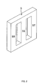
- FIG. 2 shows an example of the form of a core 5 of the Y-connection three-phase transformer.
- the windings 10R, 11R, 12R, 13R of the R-phase winding circuit are wound around an R-phase winding portion 5R of the core 5.
- the windings 10S, 11S, 12S, 13S of the S-phase winding circuit are wound around an S-phase winding portion 5S of the core 5.
- the windings 10T, 11T, 12T, 13T of the T-phase winding circuit are wound around a T-phase winding portion 5T of the core 5.
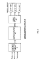
- FIG. 3 shows an example of the configuration of the switch switching circuit 8.
- the switch switching circuit 8 is configured to monitor the voltage levels of the output terminals Rout, Sout, Tout and control a group of the switches of FIG. 1 to switch between the first to fourth modes in an alternative manner such that the output voltage is within a predetermined target voltage range.
- the first switch 21R, 21S, 21T of each phase becomes ON, and all the other switches (the second, third, and fourth switches of each phase) become OFF.
- the output voltage is about 2% lower than the input voltage.
- the second switch 22R, 22S, 22T of each phase becomes ON, and all the other switches (the first, third, and fourth switches of each phase) become OFF.
- the output voltage is about 4% lower than the input voltage.
- the third switch 23R, 23S, 23T of each phase becomes ON, and all the other switches (the first, second, and fourth switches of each phase) become OFF.
- the output voltage is about 6% lower than the input voltage.
- the fourth switch 24R, 24S, 24T of each phase becomes ON, and all the other switches (the first, second, and third switches of each phase) become OFF.
- the output voltage is substantially equal to the input voltage.
- the switch switching circuit 8 comprises a voltage detecting circuit 81, a microcomputer 82, and a drive circuit 83.
- the voltage detecting circuit 81 detects the voltage levels of the output terminals Rout, Sout, Tout and inputs a detection signal to the microcomputer 82.
- the microcomputer 82 inputs control signals to the drive circuit 83 to switch between the first to fourth modes in an alternative manner.
- the drive circuit 83 switches on/off the first to fourth switches 21R to 24R of the R-phase, the first to fourth switches 21S to 24S of the S-phase, and the first to fourth switches 21T to 24T of the T-phase as described above.
- the microcomputer 82 compares the programmed target voltage range and the detection signal from the voltage detecting circuit 81, thereby monitoring whether the output voltage is higher or lower than the target voltage range (steps 410 and 420).
- the process proceeds to a voltage lowering routine of step 411 and later.
- the transformer when currently in the fourth mode (0% mode), the transformer is made to switch to the first mode (-2% mode); when currently in the first mode (-2% mode), to switch to the second mode (-4% mode); and when currently in the second mode (-4% mode), to switch to the third mode (-6% mode).
- step 421 If the output voltage is lower than the target voltage range, the process proceeds to a voltage raising routine of step 421 and later.
- the transformer when currently in the third mode (-6% mode), the transformer is made to switch to the second mode (-4% mode); when currently in the second mode (-4% mode), to switch to the first mode (-2% mode); and when currently in the first mode (-2% mode), to switch to the fourth mode (0% mode).
- the twelve switches are included in the circuit of the Y-connection three-phase transformer shown in FIG. 1 , and these switches are individually switched on/off by the drive circuit 83 shown in FIG. 3 .
- the twelve switches and their respective circuits in the drive circuit 83 are the same in configuration as one another.
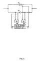
- FIG. 5 shows an example configuration of one of the twelve switches and its one corresponding circuit in the drive circuit 83.
- the switch consists of two thyristors 51, 52 connected in parallel in an opposite direction to each other.
- the drive circuit 83 comprises a gate signal generating circuit 53 and two voltage detecting circuits 54, 55.
- the gate signal generating circuit 53 outputs a gate signal G1 to turn on the thyristor 51 and a gate signal G2 to turn on the thyristor 52.
- the voltage detecting circuit 54 detects the gate-to-cathode voltage of the thyristor 51, and its output signal A becomes "1" when the gate-to-cathode voltage becomes zero (the current through the thyristor 51 becomes zero) and is at "0" when a current flows through the thyristor 51 with the gate-to-cathode voltage being not zero.
- the voltage detecting circuit 55 detects the gate-to-cathode voltage of the thyristor 52, and its output signal B becomes "1" when the gate-to-cathode voltage becomes zero (the current through the thyristor 52 becomes zero) and is at "0" when a current flows through the thyristor 5 with the gate-to-cathode voltage being not zero.
- the gate signal generating circuit 53 turns off the thyristors 51, 52 through the gate signals thereof in response to the output signals A, B of the voltage detecting circuits 54, 55 changing to "1". Further, another switch (two thyristors connected in parallel in an opposite direction to each other) to be turned on instead of the thyristors 51, 52 (one switch) turned off is turned on.
- the switch switching circuit 8 of FIG. 3 is configured to switch on/off the switches of each phase at a timing that the voltage instantaneous value of the phase becomes zero to switch the modes.
- each switch consists of thyristors connected in parallel in an opposite direction to each other, and the switch switching circuit 8 comprises the voltage detector detecting the gate-to-cathode voltage of each thyristor and is configured to turn off a thyristor with turning on another thyristor in response to a timing that its gate-to-cathode voltage is detected to have just become zero via the voltage detector of the thyristor to be turned off.
Landscapes
- Engineering & Computer Science (AREA)
- Power Engineering (AREA)
- Control Of Electrical Variables (AREA)
- Ac-Ac Conversion (AREA)
- Supply And Distribution Of Alternating Current (AREA)
Abstract
Description
- The present invention relates to a transforming apparatus which automatically adjusts the voltage of three-phase power supply led into a power consumer site to within a target voltage range lower than its rated voltage and supplies to load equipment, and particularly to such a transforming apparatus which has a Y-connection three-phase transformer as its basic configuration.
- In, for example, hotels, supermarkets, factories, etc., lighting equipment, air conditioning equipment, power equipment, or the like consumes a large amount of electric power. Recently, such general power consumers have strongly recognized the necessity for energy saving measures, and various measures have been come up with and are being carried out.
- One of energy saving measures adoptable by general power consumers is a known scheme where the electricity receiving system leading commercial power supply into indoor equipment is provided with the transforming apparatus disclosed in Japanese Patent No.
2750275 3372178 - In areas which are inferior in the stability of power generating facilities and power distribution facilities, power supply voltage at receiving points of power consumers is not stable and often fluctuates over a voltage range slightly higher than the rated voltage. In such a situation, by supplying power supply whose voltage is automatically adjusted by a transforming apparatus to a voltage several percent lower than the rated voltage to load equipment, power consumption by the load equipment is greatly reduced, thus producing an especially large energy saving effect.
- The transforming apparatus disclosed in above-cited Japanese Patent No.
3372178 - The above conventional transforming apparatus is configured to change its transformation characteristic by switching on/off a plurality of switches connecting the different phases in combination, and thus the switch needs to be switched on/off at a timing that the voltage between opposite ends of the switch (voltage between different phases) becomes zero. Hence, a switch control circuit thereof is complicated, and thus it is difficult to secure the stability and reliability of switching operation timings.
- An object of the present invention is to provide a transforming apparatus with a Y-connection three-phase transformer as its basic configuration which automatically adjusts the voltage of three-phase power supply to within a target voltage range lower than the rated voltage and supplies to load equipment.
- A transforming apparatus according to the present invention is characterized by the following items (1) to (22) :
- (1) being a transforming apparatus configured to automatically adjust the voltage of three-phase power supply comprising three input terminals (Rin, Sin, Tin), three output terminals (Rout, Sout, Tout), a Y-connection three-phase transformer, a switch group, and a switch switching circuit;
- (2) the three input terminals (Rin, Sin, Tin) being respectively connected to three main lines of the three-phase power supply;
- (3) the three output terminals (Rout, Sout, Tout) being connected to a load installation;
- (4) the Y-connection three-phase transformer comprising a core, an R-phase winding circuit, an S-phase winding circuit, and a T-phase winding circuit;
- (5) in the R-phase winding circuit, an R-phase main winding, an R-phase first auxiliary winding, an R-phase first switch, an R-phase second auxiliary winding, and an R-phase third auxiliary winding being serially connected in that order between the input terminal Rin and a neutral point O, the output terminal Rout being connected to the other end of the R-phase main winding;
- (6) an R-phase second switch of the switch group being connected in parallel with a series circuit of the R-phase first auxiliary winding and the R-phase first switch;
- (7) an R-phase third switch of the switch group being connected in parallel with a series circuit of the R-phase first auxiliary winding, the R-phase first switch, and the R-phase second auxiliary winding;
- (8) an R-phase fourth switch of the switch group being connected in parallel with a series circuit of the R-phase second auxiliary winding and the R-phase third auxiliary winding;
- (9) in the S-phase winding circuit, an S-phase main winding, an S-phase first auxiliary winding, an S-phase first switch, an S-phase second auxiliary winding, and an S-phase third auxiliary winding being serially connected in that order between the input terminal Sin and the neutral point O, the output terminal Sout being connected to the other end of the S-phase main winding;
- (10) an S-phase second switch of the switch group being connected in parallel with a series circuit of the S-phase first auxiliary winding and the S-phase first switch;
- (11) an S-phase third switch of the switch group being connected in parallel with a series circuit of the S-phase first auxiliary winding, the S-phase first switch, and the S-phase second auxiliary winding;
- (12) an S-phase fourth switch of the switch group being connected in parallel with a series circuit of the S-phase second auxiliary winding and the 5-phase third auxiliary winding;
- (13) in the T-phase winding circuit, a T-phase main winding, a T-phase first auxiliary winding, a T-phase first switch, a T-phase second auxiliary winding, and a T-phase third auxiliary winding being serially connected in that order between the input terminal Tin and the neutral point O, the output terminal Tout being connected to the other end of the T-phase main winding;
- (14) a T-phase second switch of the switch group being connected in parallel with a series circuit of the T-phase first auxiliary winding and the T-phase first switch;
- (15) a T-phase third switch of the switch group being connected in parallel with a series circuit of the T-phase first auxiliary winding, the T-phase first switch, and the T-phase second auxiliary winding;
- (16) a T-phase fourth switch of the switch group being connected in parallel with a series circuit of the T-phase second auxiliary winding and the T-phase third auxiliary winding;
- (17) the switch switching circuit configured to control the switches based on the voltage levels of the output terminals (Rout, Sout, Tout) or the input terminals (Rin, Sin, Tin) in order to switch between first to fourth modes in an alternative manner;
- (18) in the first mode, the first switch of each phase being ON, and the second, third, and fourth switches of each phase being OFF;
- (19) in the second mode, the second switch of each phase being ON, and the first, third, and fourth switches of each phase being OFF;
- (20) in the third mode, the third switch of each phase being ON, and the first, second, and fourth switches of each phase being OFF;
- (21) in the fourth mode, the fourth switch of each phase being ON, and the first, second, and third switches of each phase being OFF; and
- (22) the switch switching circuit configured to switch on/off the switches of each phase at a timing that the voltage instantaneous value of the phase becomes zero to switch the modes.
-
-
FIG. 1 is a winding configuration diagram of a transforming apparatus according to an embodiment of the present invention; -
FIG. 2 is a configuration diagram of a core according to the embodiment of the present invention; -
FIG. 3 shows the configuration of a switch switching circuit according to the embodiment of the present invention; -
FIG. 4 is a flow chart of the process procedure by amicrocomputer 82 in the embodiment; and -
FIG. 5 shows an example configuration of one switch and its corresponding part in the switch switching circuit. - Rin, Sin, Tin Input terminal
Rout, Sout, Tout Output terminal
10R R-phase main winding
11R R-phase first auxiliary winding
12R R-phase second auxiliary winding
13R R-phase third auxiliary winding
21R R-phase first switch
22R R-phase second switch
23R R-phase third switch
24R R-phase fourth switch
10S S-phase main winding
11S S-phase first auxiliary winding
12S S-phase second auxiliary winding
13S S-phase third auxiliary winding
21S S-phase first switch
22S S-phase second switch
23S S-phase third switch
24S S-phase fourth switch
10T T-phase main winding
11T T-phase first auxiliary winding
12T T-phase second auxiliary winding
13T T-phase third auxiliary winding
21T T-phase first switch
22T T-phase second switch
23T T-phase third switch
24T T-phase fourth switch
5 Core
5R R-phase winding portion
5S S-phase winding portion
5T T-phase winding portion
8 Switch switching circuit
81 Voltage detecting circuit
82 Microcomputer
83 Drive circuit
51, 52 Thyristor
53 Gate signal generating circuit
54, 55 Voltage detecting circuit -
FIG. 1 shows the winding configuration of a transforming apparatus according to the present invention, andFIG. 3 shows the configuration of aswitch switching circuit 8. First, the overall outline of this transforming apparatus will be described. - This transforming apparatus comprises three input terminals Rin, Sin, Tin connected respectively to the three main lines of three-phase power supply and three output terminals Rout, Sout, Tout connected to a load installation. The transforming apparatus switches between a first mode where the output voltage is made about 2% lower than the input voltage, a second mode where the output voltage is made about 4% lower than the input voltage, a third mode where the output voltage is made about 6% lower than the input voltage, and a fourth mode where the output voltage is substantially equal to the input voltage in an alternative manner.
- The transforming apparatus comprises, as its basic configuration, a Y-connection three-phase transformer made up of an R-phase winding circuit, an S-phase winding circuit, and a T-phase winding circuit, which are the same in configuration, as shown in
FIG. 1 . - In the R-phase winding circuit, an R-phase main winding 10R, an R-phase first auxiliary winding 11R, an R-phase
first switch 21R, an R-phase second auxiliary winding 12R, and an R-phase third auxiliary winding 13R are serially connected in that order between the input terminal Rin and a neutral point O. The output terminal Rout is connected to the other end of the R-phase main winding 10R. - An R-phase second switch 22R is connected in parallel with a series circuit of the R-phase first auxiliary winding 11R and the R-phase
first switch 21R. - An R-phase third switch 23R is connected in parallel with a series circuit of the R-phase first auxiliary winding 11R, the R-phase
first switch 21R, and the R-phase second auxiliary winding 12R. - An R-phase
fourth switch 24R is connected in parallel with a series circuit of the R-phase second auxiliary winding 12R and the R-phase third auxiliary winding 13R. - In the S-phase winding circuit, an S-phase main winding 10S, an S-phase first auxiliary winding 11S, an S-phase
first switch 21S, an S-phase second auxiliary winding 12S, and an S-phase third auxiliary winding 13S are serially connected in that order between the input terminal Sin and the neutral point O. The output terminal Sout is connected to the other end of the S-phase main winding 10S. - An S-phase
second switch 22S is connected in parallel with a series circuit of the S-phase first auxiliary winding 11S and the S-phasefirst switch 21S. - An S-phase
third switch 23S is connected in parallel with a series circuit of the S-phase first auxiliary winding 11S, the S-phasefirst switch 21S, and the S-phase second auxiliary winding 12S. - An S-phase
fourth switch 24S is connected in parallel with a series circuit of the S-phase second auxiliary winding 12S and the S-phase third auxiliary winding 13S. - In the T-phase winding circuit, a T-phase main winding 10T, a T-phase first auxiliary winding 11T, a T-phase
first switch 21T, a T-phase second auxiliary winding 12T, and a T-phase third auxiliary winding 13T are serially connected in that order between the input terminal Tin and the neutral point O. The output terminal Tout is connected to the other end of the T-phase main winding 10T. - A T-phase
second switch 22T is connected in parallel with a series circuit of the T-phase first auxiliary winding 11T and the T-phasefirst switch 21T. - A T-phase
third switch 23T is connected in parallel with a series circuit of the T-phase first auxiliary winding 11T, the T-phasefirst switch 21T, and the T-phase second auxiliary winding 12T. - A T-phase
fourth switch 24T is connected in parallel with a series circuit of the T-phase second auxiliary winding 12T and the T-phase third auxiliary winding 13T. ===Example ofcore 5=== -
FIG. 2 shows an example of the form of acore 5 of the Y-connection three-phase transformer. Thewindings phase winding portion 5R of thecore 5. Thewindings phase winding portion 5S of thecore 5. Thewindings phase winding portion 5T of thecore 5. -
FIG. 3 shows an example of the configuration of theswitch switching circuit 8. Theswitch switching circuit 8 is configured to monitor the voltage levels of the output terminals Rout, Sout, Tout and control a group of the switches ofFIG. 1 to switch between the first to fourth modes in an alternative manner such that the output voltage is within a predetermined target voltage range. - In the first mode, the
first switch - In the second mode, the
second switch - In the third mode, the
third switch - In the fourth mode, the
fourth switch - As shown in
FIG. 3 , theswitch switching circuit 8 comprises avoltage detecting circuit 81, amicrocomputer 82, and adrive circuit 83. Thevoltage detecting circuit 81 detects the voltage levels of the output terminals Rout, Sout, Tout and inputs a detection signal to themicrocomputer 82. Performing a process shown in the flow chart ofFIG. 4 based on the detection signal from thevoltage detecting circuit 81, themicrocomputer 82 inputs control signals to thedrive circuit 83 to switch between the first to fourth modes in an alternative manner. According to the control signals from themicrocomputer 82, thedrive circuit 83 switches on/off the first tofourth switches 21R to 24R of the R-phase, the first tofourth switches 21S to 24S of the S-phase, and the first tofourth switches 21T to 24T of the T-phase as described above. - An example of the process procedure of the
microcomputer 82 will be described with reference to the flow chart ofFIG. 4 . Themicrocomputer 82 compares the programmed target voltage range and the detection signal from thevoltage detecting circuit 81, thereby monitoring whether the output voltage is higher or lower than the target voltage range (steps 410 and 420). - If the output voltage is higher than the target voltage range, the process proceeds to a voltage lowering routine of
step 411 and later. In the voltage lowering routine, when currently in the fourth mode (0% mode), the transformer is made to switch to the first mode (-2% mode); when currently in the first mode (-2% mode), to switch to the second mode (-4% mode); and when currently in the second mode (-4% mode), to switch to the third mode (-6% mode). - If the output voltage is lower than the target voltage range, the process proceeds to a voltage raising routine of
step 421 and later. In the voltage raising routine, when currently in the third mode (-6% mode), the transformer is made to switch to the second mode (-4% mode); when currently in the second mode (-4% mode), to switch to the first mode (-2% mode); and when currently in the first mode (-2% mode), to switch to the fourth mode (0% mode). - As described above, the twelve switches are included in the circuit of the Y-connection three-phase transformer shown in
FIG. 1 , and these switches are individually switched on/off by thedrive circuit 83 shown inFIG. 3 . The twelve switches and their respective circuits in thedrive circuit 83 are the same in configuration as one another. -
FIG. 5 shows an example configuration of one of the twelve switches and its one corresponding circuit in thedrive circuit 83. The switch consists of twothyristors drive circuit 83 comprises a gatesignal generating circuit 53 and twovoltage detecting circuits signal generating circuit 53 outputs a gate signal G1 to turn on thethyristor 51 and a gate signal G2 to turn on thethyristor 52. - The
voltage detecting circuit 54 detects the gate-to-cathode voltage of thethyristor 51, and its output signal A becomes "1" when the gate-to-cathode voltage becomes zero (the current through thethyristor 51 becomes zero) and is at "0" when a current flows through thethyristor 51 with the gate-to-cathode voltage being not zero. - Likewise, the
voltage detecting circuit 55 detects the gate-to-cathode voltage of thethyristor 52, and its output signal B becomes "1" when the gate-to-cathode voltage becomes zero (the current through thethyristor 52 becomes zero) and is at "0" when a current flows through thethyristor 5 with the gate-to-cathode voltage being not zero. - When the
microcomputer 82 ofFIG. 3 gives thedrive circuit 83 ofFIG. 3 (including the gate signal generating circuit 53) a control signal to instruct to turn off thethyristors 51, 52 (one switch), the gatesignal generating circuit 53 turns off thethyristors voltage detecting circuits thyristors 51, 52 (one switch) turned off is turned on. - As such, the
switch switching circuit 8 ofFIG. 3 is configured to switch on/off the switches of each phase at a timing that the voltage instantaneous value of the phase becomes zero to switch the modes. In the above embodiment, each switch consists of thyristors connected in parallel in an opposite direction to each other, and theswitch switching circuit 8 comprises the voltage detector detecting the gate-to-cathode voltage of each thyristor and is configured to turn off a thyristor with turning on another thyristor in response to a timing that its gate-to-cathode voltage is detected to have just become zero via the voltage detector of the thyristor to be turned off.
Claims (2)
- A transforming apparatus configured to automatically adjust the voltage of three-phase power supply comprising:three input terminals (Rin, Sin, Tin);three output terminals (Rout, Sout, Tout);a Y-connection three-phase transformersa switch group (21R-24R, 21S-24S, 21T-24T), characterized bya switch switching circuit (8), wherein;the three input terminals (Rin, Sin, Tin) are respectively connected to three main lines of the three-phase power supply;the three output terminals (Rout, Sout, Tout) are connected to a load installation;the Y-connection three-phase transformer comprises a core (5), an R-phase winding circuit, an S-phase winding circuit, and a T-phase winding circuit;in the 12-phase winding circuit, an R-phase main winding (10R), an R-phase first auxiliary winding (11R), an R-phase first switch (21R), an R-phase second auxiliary winding (12R), and an R-phase third auxiliary winding (13R) are serially connected in that order between the input terminal Rin and a neutral point 0, the output terminal Rout being connected to the other end of the R-phase main winding (10R);an R-phase second switch (22R) of the switch group is connected in parallel with a series circuit of the R-phase first auxiliary winding (11R) and the R-phase first switch (21R);an R-phase third switch (23R) of the switch group is connected in parallel with a series circuit of the R-phase first auxiliary winding (11R), the R-phase first switch (21R), and the R-phase second auxiliary winding (12R);an R-phase fourth switch (24R) of the switch group is connected in parallel with a series circuit of the R-phase second auxiliary winding (12R) and the R-phase third auxiliary winding (13R);in the S-phase winding circuit, an S-phase main winding (10S), an S-phase first auxiliary winding (11S), an S-phase first switch (21S), an S-phase second auxiliary winding (12S), and an S-phase third auxiliary winding (13S) are serially connected in that order between the input terminal Sin and the neutral point 0, the output terminal Sout being connected to the other end of the S-phase main winding (10S);an S-phase second switch (22S) of the switch group is connected in parallel with a series circuit of the S-phase first auxiliary winding (11S) and the S-phase first switch (21S);an S-phase third switch (23S) of the switch group is connected in parallel with a series circuit of the S-phase first auxiliary winding (11S), the S-phase first switch (21S), and the S-phase second auxiliary winding (12S);an S-phase fourth switch (24S) of the switch group is connected in parallel with a series circuit of the S-phase second auxiliary winding (12S) and the S-phase third auxiliary winding (13S);in the T-phase winding circuit, a T-phase main winding (10T), a T-phase first auxiliary winding (11T), a T-phase first switch (21T), a T-phase second auxiliary winding (12T), and a T-phase third auxiliary winding (13T) are serially connected in that order between the input terminal Tin and the neutral point 0, the output terminal Tout being connected to the other end of the T-phase main winding (10T);a T-phase second switch (22T) of the switch group is connected in parallel with a series circuit of the T-phase first auxiliary winding (11T) and the T-phase first switch (21T);a T-phase third switch (23T) of the switch group is connected in parallel with a series circuit of the T-phase first auxiliary winding (11T), the T-phase first switch (21T), and the T-phase second auxiliary winding (12T);a T-phase fourth switch (24R) of the switch group is connected in parallel with a series circuit of the T-phase second auxiliary winding (12T) and the T-phase third auxiliary winding (13T);the switch switching circuit (8) is configured to control the switches based on the voltage levels of the output terminals (Rout, Sout, Tout) or the input terminals (Rin, Sin, Tin) in order to switch between first to fourth modes in an alternative manner such that;in the first mode, the first switch (21R, 21S, 21T) of each phase is ON, and the second (22R, 22S, 22T), third (23R, 23S, 23T), and fourth (24R, 24S, 24T) switches of each phase are OFF;in the second mode, the second switch (22R, 22S, 22T) of each phase is ON, and the first (21R, 21S, 21T), third (23R, 23S, 23T), and fourth (24R, 24S, 24T) switches of each phase are OFF;in the third mode, the third switch (23R, 23S, 23T) of each phase is ON, and the first (21R, 21S, 21T), second (22R, 22S, 22T), and fourth (24R, 245, 24T) switches of each phase are OFF;in the fourth mode, the fourth switch (24R, 24S, 24T) of each phase is ON, and the first (21R, 21S, 21T), second (22R, 22S, 22T), and third (23R, 23S, 23T) switches of each phase are OFF; andthe switch switching circuit (8) is configured to switch on/off the switches of each phase at a timing that the voltage instantaneous value of the phase becomes zero to switch the modes.
- The transforming apparatus according to claim 1, wherein each of the switches includes (21R-24R, 21S-24S, 21T-24T) thyristors (51, 52) connected in parallel in an opposite direction to each other, and the switch switching circuit (8) comprises a voltage detector (54, 55) configured to detect the gate-to-cathode voltage of each of the thyristors and turns off a thyristor with turning on another thyristor in response to a timing that its gate-to-cathode voltage is detected to have just become zero via the voltage detector of the thyristor to be turned off.
Applications Claiming Priority (1)
| Application Number | Priority Date | Filing Date | Title |
|---|---|---|---|
| PCT/JP2008/063267 WO2009136451A1 (en) | 2008-07-24 | 2008-07-24 | Transformation device for automatically adjusting voltage of three-phase power supply |
Publications (4)
| Publication Number | Publication Date |
|---|---|
| EP2139089A1 EP2139089A1 (en) | 2009-12-30 |
| EP2139089A4 EP2139089A4 (en) | 2010-06-16 |
| EP2139089B1 true EP2139089B1 (en) | 2011-07-20 |
| EP2139089B8 EP2139089B8 (en) | 2011-10-05 |
Family
ID=41036711
Family Applications (1)
| Application Number | Title | Priority Date | Filing Date |
|---|---|---|---|
| EP08791519A Not-in-force EP2139089B8 (en) | 2008-07-24 | 2008-07-24 | Transformation device for automatically adjusting voltage of three-phase power supply |
Country Status (13)
| Country | Link |
|---|---|
| US (1) | US7786717B2 (en) |
| EP (1) | EP2139089B8 (en) |
| JP (1) | JP4312826B1 (en) |
| CN (1) | CN101689759B (en) |
| AR (1) | AR069069A1 (en) |
| AT (1) | ATE517456T1 (en) |
| BR (1) | BRPI0804505A2 (en) |
| CA (1) | CA2646173C (en) |
| ES (1) | ES2395064T3 (en) |
| HK (1) | HK1139517A1 (en) |
| MX (1) | MX2008016544A (en) |
| TW (1) | TWI320985B (en) |
| WO (1) | WO2009136451A1 (en) |
Cited By (1)
| Publication number | Priority date | Publication date | Assignee | Title |
|---|---|---|---|---|
| DE102016218439A1 (en) | 2016-09-26 | 2018-03-29 | Bayerische Motoren Werke Aktiengesellschaft | Construction of a local three-phase power grid |
Families Citing this family (6)
| Publication number | Priority date | Publication date | Assignee | Title |
|---|---|---|---|---|
| WO2012126860A2 (en) | 2011-03-18 | 2012-09-27 | Powerperfector Limited | A controller for a transformer |
| US20150247886A1 (en) * | 2014-02-28 | 2015-09-03 | International Business Machines Corporation | Transformer Phase Permutation Causing More Uniform Transformer Phase Aging and general switching network suitable for same |
| CN108282042A (en) * | 2018-01-19 | 2018-07-13 | 华中科技大学 | A kind of speed governing permanent magnet synchronous motor based on change umber of turn |
| CN111478642B (en) * | 2020-04-16 | 2022-03-01 | 广州华凌制冷设备有限公司 | Drive control circuit, drive control method, circuit board and air conditioner |
| WO2022125255A1 (en) * | 2020-12-07 | 2022-06-16 | S&C Electric Company | Phase balancing and lv mesh switching |
| CN114069607B (en) * | 2021-10-08 | 2024-05-14 | 井上和一 | Intelligent voltage control method and control system |
Family Cites Families (8)
| Publication number | Priority date | Publication date | Assignee | Title |
|---|---|---|---|---|
| JPH0645320A (en) | 1992-07-27 | 1994-02-18 | Nec Corp | Manufacture of semiconductor device and manufacturing device thereof |
| JPH0645320U (en) | 1992-11-24 | 1994-06-14 | 株式会社明電舎 | Voltage regulator with built-in transformer |
| JP2996377B2 (en) * | 1993-07-10 | 1999-12-27 | 永田 勝彦 | A device that controls the step-down ratio of an autotransformer according to the AC input voltage |
| JP2750275B2 (en) * | 1995-01-10 | 1998-05-13 | 愛好電機株式会社 | Power-saving transformer with autonomous switching device |
| WO1997002518A1 (en) | 1995-06-12 | 1997-01-23 | Nariisa Imoto | Voltage regulator |
| JPH09247857A (en) | 1996-01-05 | 1997-09-19 | Kawamura Electric Inc | Power saving device |
| JP3372178B2 (en) * | 1996-12-25 | 2003-01-27 | 愛好電機株式会社 | Power saving device with three-phase automatic voltage switching device |
| JP2000125473A (en) | 1998-10-19 | 2000-04-28 | Toshiba Corp | Power regulator and control method for the regulator |
-
2008
- 2008-07-24 EP EP08791519A patent/EP2139089B8/en not_active Not-in-force
- 2008-07-24 ES ES08791519T patent/ES2395064T3/en active Active
- 2008-07-24 JP JP2008554355A patent/JP4312826B1/en not_active Expired - Fee Related
- 2008-07-24 US US12/377,920 patent/US7786717B2/en not_active Expired - Fee Related
- 2008-07-24 WO PCT/JP2008/063267 patent/WO2009136451A1/en active Application Filing
- 2008-07-24 CN CN2008800002921A patent/CN101689759B/en not_active Expired - Fee Related
- 2008-07-24 MX MX2008016544A patent/MX2008016544A/en active IP Right Grant
- 2008-07-24 BR BRPI0804505-4A patent/BRPI0804505A2/en not_active IP Right Cessation
- 2008-07-24 AT AT08791519T patent/ATE517456T1/en not_active IP Right Cessation
- 2008-07-24 CA CA2646173A patent/CA2646173C/en not_active Expired - Fee Related
- 2008-12-03 TW TW097146982A patent/TWI320985B/en not_active IP Right Cessation
- 2008-12-09 AR ARP080105325A patent/AR069069A1/en active IP Right Grant
-
2010
- 2010-06-25 HK HK10106264.4A patent/HK1139517A1/en not_active IP Right Cessation
Cited By (1)
| Publication number | Priority date | Publication date | Assignee | Title |
|---|---|---|---|---|
| DE102016218439A1 (en) | 2016-09-26 | 2018-03-29 | Bayerische Motoren Werke Aktiengesellschaft | Construction of a local three-phase power grid |
Also Published As
| Publication number | Publication date |
|---|---|
| ATE517456T1 (en) | 2011-08-15 |
| CA2646173A1 (en) | 2009-10-23 |
| EP2139089B8 (en) | 2011-10-05 |
| MX2008016544A (en) | 2010-02-17 |
| CN101689759B (en) | 2012-11-28 |
| JP4312826B1 (en) | 2009-08-12 |
| CN101689759A (en) | 2010-03-31 |
| JPWO2009136451A1 (en) | 2011-09-01 |
| TWI320985B (en) | 2010-02-21 |
| US20100164444A1 (en) | 2010-07-01 |
| EP2139089A4 (en) | 2010-06-16 |
| WO2009136451A1 (en) | 2009-11-12 |
| TW201006088A (en) | 2010-02-01 |
| ES2395064T3 (en) | 2013-02-07 |
| CA2646173C (en) | 2011-08-02 |
| AR069069A1 (en) | 2009-12-30 |
| HK1139517A1 (en) | 2010-09-17 |
| US7786717B2 (en) | 2010-08-31 |
| BRPI0804505A2 (en) | 2011-08-30 |
| EP2139089A1 (en) | 2009-12-30 |
Similar Documents
| Publication | Publication Date | Title |
|---|---|---|
| EP2139089B1 (en) | Transformation device for automatically adjusting voltage of three-phase power supply | |
| GB2580748A (en) | Controlling voltage in AC power lines | |
| WO1998029788A1 (en) | Method and device for automatically switching three-phase voltage for power saving transformer | |
| EP2044684B1 (en) | Variable voltage supply system | |
| AU2008255124B2 (en) | Transforming apparatus for automatically adjusting three-phase power supply voltage | |
| JP5731143B2 (en) | Voltage regulator | |
| WO2008044374A1 (en) | Method for detecting turn-off of thyristor | |
| KR200392618Y1 (en) | Electric power saver of saturable reactor using tap select method | |
| KR100519380B1 (en) | 3 phase no-power-cut tap-switching transformer system | |
| KR20100011876A (en) | Transforming apparatus for automatically adjusting three-phase power supply voltage | |
| JP2015050881A (en) | Power factor automatic adjuster | |
| JP2003299361A (en) | Low-voltage automatic voltage regulator | |
| CN211859614U (en) | Three-phase unbalanced power generator | |
| WO2021000610A1 (en) | Voltage balancing and stabilizing apparatus and method | |
| KR20060118930A (en) | Linear AC Power Control Device Using Phase Comparison Control | |
| JPH0746763A (en) | Reactive power regulator | |
| KR100709621B1 (en) | Distributing box for street light | |
| JP2000148267A (en) | Alternating-current power unit | |
| KR200410123Y1 (en) | Distributing box for street light | |
| CN205305210U (en) | Energy -conserving cabinet of illumination steady voltage | |
| CN117461254A (en) | Method and system for operating a regulating transformer | |
| KR20230108590A (en) | Device providing lagging reactive power and method for controlling temperature correction thereof | |
| KR200417768Y1 (en) | Electric saving device for home with automatic tap adjustment | |
| KR20090085009A (en) | Electric saving device with automatic tap adjustment | |
| JPH0767339A (en) | Method for improving power factor of primary side of ac line of controlled rectifier |
Legal Events
| Date | Code | Title | Description |
|---|---|---|---|
| PUAI | Public reference made under article 153(3) epc to a published international application that has entered the european phase |
Free format text: ORIGINAL CODE: 0009012 |
|
| 17P | Request for examination filed |
Effective date: 20090316 |
|
| AK | Designated contracting states |
Kind code of ref document: A1 Designated state(s): AT BE BG CH CY CZ DE DK EE ES FI FR GB GR HR HU IE IS IT LI LT LU LV MC MT NL NO PL PT RO SE SI SK TR |
|
| A4 | Supplementary search report drawn up and despatched |
Effective date: 20100520 |
|
| RIC1 | Information provided on ipc code assigned before grant |
Ipc: H02J 3/18 20060101AFI20100512BHEP Ipc: H01F 29/02 20060101ALN20100512BHEP |
|
| REG | Reference to a national code |
Ref country code: HK Ref legal event code: DE Ref document number: 1139517 Country of ref document: HK |
|
| GRAP | Despatch of communication of intention to grant a patent |
Free format text: ORIGINAL CODE: EPIDOSNIGR1 |
|
| RIC1 | Information provided on ipc code assigned before grant |
Ipc: H01F 29/02 20060101ALN20101105BHEP Ipc: H02J 3/18 20060101AFI20101105BHEP |
|
| DAX | Request for extension of the european patent (deleted) | ||
| GRAS | Grant fee paid |
Free format text: ORIGINAL CODE: EPIDOSNIGR3 |
|
| RIN1 | Information on inventor provided before grant (corrected) |
Inventor name: TSUNEMI, SEIJI Inventor name: SHIMAZU, CHIYUKI |
|
| GRAA | (expected) grant |
Free format text: ORIGINAL CODE: 0009210 |
|
| AK | Designated contracting states |
Kind code of ref document: B1 Designated state(s): AT BE BG CH CY CZ DE DK EE ES FI FR GB GR HR HU IE IS IT LI LT LU LV MC MT NL NO PL PT RO SE SI SK TR |
|
| REG | Reference to a national code |
Ref country code: GB Ref legal event code: FG4D |
|
| REG | Reference to a national code |
Ref country code: CH Ref legal event code: EP |
|
| RAP2 | Party data changed (patent owner data changed or rights of a patent transferred) |
Owner name: POWERPERFECTOR LIMITED |
|
| REG | Reference to a national code |
Ref country code: DE Ref legal event code: R096 Ref document number: 602008008405 Country of ref document: DE Effective date: 20110908 |
|
| REG | Reference to a national code |
Ref country code: NL Ref legal event code: VDEP Effective date: 20110720 |
|
| PG25 | Lapsed in a contracting state [announced via postgrant information from national office to epo] |
Ref country code: MT Free format text: LAPSE BECAUSE OF FAILURE TO SUBMIT A TRANSLATION OF THE DESCRIPTION OR TO PAY THE FEE WITHIN THE PRESCRIBED TIME-LIMIT Effective date: 20110720 |
|
| REG | Reference to a national code |
Ref country code: AT Ref legal event code: MK05 Ref document number: 517456 Country of ref document: AT Kind code of ref document: T Effective date: 20110720 |
|
| PG25 | Lapsed in a contracting state [announced via postgrant information from national office to epo] |
Ref country code: FI Free format text: LAPSE BECAUSE OF FAILURE TO SUBMIT A TRANSLATION OF THE DESCRIPTION OR TO PAY THE FEE WITHIN THE PRESCRIBED TIME-LIMIT Effective date: 20110720 Ref country code: BE Free format text: LAPSE BECAUSE OF FAILURE TO SUBMIT A TRANSLATION OF THE DESCRIPTION OR TO PAY THE FEE WITHIN THE PRESCRIBED TIME-LIMIT Effective date: 20110720 Ref country code: HR Free format text: LAPSE BECAUSE OF FAILURE TO SUBMIT A TRANSLATION OF THE DESCRIPTION OR TO PAY THE FEE WITHIN THE PRESCRIBED TIME-LIMIT Effective date: 20110720 Ref country code: NO Free format text: LAPSE BECAUSE OF FAILURE TO SUBMIT A TRANSLATION OF THE DESCRIPTION OR TO PAY THE FEE WITHIN THE PRESCRIBED TIME-LIMIT Effective date: 20111020 Ref country code: SE Free format text: LAPSE BECAUSE OF FAILURE TO SUBMIT A TRANSLATION OF THE DESCRIPTION OR TO PAY THE FEE WITHIN THE PRESCRIBED TIME-LIMIT Effective date: 20110720 Ref country code: PT Free format text: LAPSE BECAUSE OF FAILURE TO SUBMIT A TRANSLATION OF THE DESCRIPTION OR TO PAY THE FEE WITHIN THE PRESCRIBED TIME-LIMIT Effective date: 20111121 Ref country code: NL Free format text: LAPSE BECAUSE OF FAILURE TO SUBMIT A TRANSLATION OF THE DESCRIPTION OR TO PAY THE FEE WITHIN THE PRESCRIBED TIME-LIMIT Effective date: 20110720 Ref country code: IS Free format text: LAPSE BECAUSE OF FAILURE TO SUBMIT A TRANSLATION OF THE DESCRIPTION OR TO PAY THE FEE WITHIN THE PRESCRIBED TIME-LIMIT Effective date: 20111120 Ref country code: LT Free format text: LAPSE BECAUSE OF FAILURE TO SUBMIT A TRANSLATION OF THE DESCRIPTION OR TO PAY THE FEE WITHIN THE PRESCRIBED TIME-LIMIT Effective date: 20110720 |
|
| PG25 | Lapsed in a contracting state [announced via postgrant information from national office to epo] |
Ref country code: SI Free format text: LAPSE BECAUSE OF FAILURE TO SUBMIT A TRANSLATION OF THE DESCRIPTION OR TO PAY THE FEE WITHIN THE PRESCRIBED TIME-LIMIT Effective date: 20110720 Ref country code: CY Free format text: LAPSE BECAUSE OF FAILURE TO SUBMIT A TRANSLATION OF THE DESCRIPTION OR TO PAY THE FEE WITHIN THE PRESCRIBED TIME-LIMIT Effective date: 20110720 Ref country code: MC Free format text: LAPSE BECAUSE OF NON-PAYMENT OF DUE FEES Effective date: 20110731 Ref country code: PL Free format text: LAPSE BECAUSE OF FAILURE TO SUBMIT A TRANSLATION OF THE DESCRIPTION OR TO PAY THE FEE WITHIN THE PRESCRIBED TIME-LIMIT Effective date: 20110720 Ref country code: LV Free format text: LAPSE BECAUSE OF FAILURE TO SUBMIT A TRANSLATION OF THE DESCRIPTION OR TO PAY THE FEE WITHIN THE PRESCRIBED TIME-LIMIT Effective date: 20110720 Ref country code: AT Free format text: LAPSE BECAUSE OF FAILURE TO SUBMIT A TRANSLATION OF THE DESCRIPTION OR TO PAY THE FEE WITHIN THE PRESCRIBED TIME-LIMIT Effective date: 20110720 Ref country code: GR Free format text: LAPSE BECAUSE OF FAILURE TO SUBMIT A TRANSLATION OF THE DESCRIPTION OR TO PAY THE FEE WITHIN THE PRESCRIBED TIME-LIMIT Effective date: 20111021 |
|
| REG | Reference to a national code |
Ref country code: DE Ref legal event code: R081 Ref document number: 602008008405 Country of ref document: DE Owner name: POWERPERFECTOR LIMITED, GB Free format text: FORMER OWNER: E-FOUR CORPORATION, SAITAMA, JP Effective date: 20120105 Ref country code: DE Ref legal event code: R081 Ref document number: 602008008405 Country of ref document: DE Owner name: INTELLIGENT ENERGY SAVING COMPANY LIMITED, GB Free format text: FORMER OWNER: E-FOUR CORPORATION, SAITAMA, JP Effective date: 20120105 |
|
| REG | Reference to a national code |
Ref country code: IE Ref legal event code: MM4A |
|
| PG25 | Lapsed in a contracting state [announced via postgrant information from national office to epo] |
Ref country code: CZ Free format text: LAPSE BECAUSE OF FAILURE TO SUBMIT A TRANSLATION OF THE DESCRIPTION OR TO PAY THE FEE WITHIN THE PRESCRIBED TIME-LIMIT Effective date: 20110720 Ref country code: SK Free format text: LAPSE BECAUSE OF FAILURE TO SUBMIT A TRANSLATION OF THE DESCRIPTION OR TO PAY THE FEE WITHIN THE PRESCRIBED TIME-LIMIT Effective date: 20110720 |
|
| REG | Reference to a national code |
Ref country code: HK Ref legal event code: GR Ref document number: 1139517 Country of ref document: HK |
|
| PLBE | No opposition filed within time limit |
Free format text: ORIGINAL CODE: 0009261 |
|
| STAA | Information on the status of an ep patent application or granted ep patent |
Free format text: STATUS: NO OPPOSITION FILED WITHIN TIME LIMIT |
|
| PG25 | Lapsed in a contracting state [announced via postgrant information from national office to epo] |
Ref country code: RO Free format text: LAPSE BECAUSE OF FAILURE TO SUBMIT A TRANSLATION OF THE DESCRIPTION OR TO PAY THE FEE WITHIN THE PRESCRIBED TIME-LIMIT Effective date: 20110720 Ref country code: EE Free format text: LAPSE BECAUSE OF FAILURE TO SUBMIT A TRANSLATION OF THE DESCRIPTION OR TO PAY THE FEE WITHIN THE PRESCRIBED TIME-LIMIT Effective date: 20110720 |
|
| 26N | No opposition filed |
Effective date: 20120423 |
|
| PG25 | Lapsed in a contracting state [announced via postgrant information from national office to epo] |
Ref country code: DK Free format text: LAPSE BECAUSE OF FAILURE TO SUBMIT A TRANSLATION OF THE DESCRIPTION OR TO PAY THE FEE WITHIN THE PRESCRIBED TIME-LIMIT Effective date: 20110720 |
|
| REG | Reference to a national code |
Ref country code: FR Ref legal event code: ST Effective date: 20120525 |
|
| PG25 | Lapsed in a contracting state [announced via postgrant information from national office to epo] |
Ref country code: IE Free format text: LAPSE BECAUSE OF NON-PAYMENT OF DUE FEES Effective date: 20110724 |
|
| REG | Reference to a national code |
Ref country code: DE Ref legal event code: R097 Ref document number: 602008008405 Country of ref document: DE Effective date: 20120423 |
|
| PG25 | Lapsed in a contracting state [announced via postgrant information from national office to epo] |
Ref country code: FR Free format text: LAPSE BECAUSE OF NON-PAYMENT OF DUE FEES Effective date: 20110920 |
|
| REG | Reference to a national code |
Ref country code: ES Ref legal event code: FG2A Ref document number: 2395064 Country of ref document: ES Kind code of ref document: T3 Effective date: 20130207 |
|
| REG | Reference to a national code |
Ref country code: CH Ref legal event code: PL |
|
| PG25 | Lapsed in a contracting state [announced via postgrant information from national office to epo] |
Ref country code: LI Free format text: LAPSE BECAUSE OF NON-PAYMENT OF DUE FEES Effective date: 20120731 Ref country code: CH Free format text: LAPSE BECAUSE OF NON-PAYMENT OF DUE FEES Effective date: 20120731 |
|
| PG25 | Lapsed in a contracting state [announced via postgrant information from national office to epo] |
Ref country code: LU Free format text: LAPSE BECAUSE OF NON-PAYMENT OF DUE FEES Effective date: 20110724 |
|
| PG25 | Lapsed in a contracting state [announced via postgrant information from national office to epo] |
Ref country code: BG Free format text: LAPSE BECAUSE OF FAILURE TO SUBMIT A TRANSLATION OF THE DESCRIPTION OR TO PAY THE FEE WITHIN THE PRESCRIBED TIME-LIMIT Effective date: 20111020 |
|
| PG25 | Lapsed in a contracting state [announced via postgrant information from national office to epo] |
Ref country code: TR Free format text: LAPSE BECAUSE OF FAILURE TO SUBMIT A TRANSLATION OF THE DESCRIPTION OR TO PAY THE FEE WITHIN THE PRESCRIBED TIME-LIMIT Effective date: 20110720 |
|
| PG25 | Lapsed in a contracting state [announced via postgrant information from national office to epo] |
Ref country code: HU Free format text: LAPSE BECAUSE OF FAILURE TO SUBMIT A TRANSLATION OF THE DESCRIPTION OR TO PAY THE FEE WITHIN THE PRESCRIBED TIME-LIMIT Effective date: 20110720 |
|
| REG | Reference to a national code |
Ref country code: GB Ref legal event code: 732E Free format text: REGISTERED BETWEEN 20160804 AND 20160810 |
|
| REG | Reference to a national code |
Ref country code: ES Ref legal event code: PC2A Owner name: INTELLIGENT ENERGY SAVING COMPANY LIMITED Effective date: 20160914 |
|
| REG | Reference to a national code |
Ref country code: DE Ref legal event code: R082 Ref document number: 602008008405 Country of ref document: DE Representative=s name: VKK PATENTANWAELTE, DE Ref country code: DE Ref legal event code: R081 Ref document number: 602008008405 Country of ref document: DE Owner name: INTELLIGENT ENERGY SAVING COMPANY LIMITED, GB Free format text: FORMER OWNER: POWERPERFECTOR LIMITED, LONDON, GB Ref country code: DE Ref legal event code: R082 Ref document number: 602008008405 Country of ref document: DE Representative=s name: VKK PATENTANWAELTE PARTG MBB, DE |
|
| PGFP | Annual fee paid to national office [announced via postgrant information from national office to epo] |
Ref country code: DE Payment date: 20170719 Year of fee payment: 10 Ref country code: IT Payment date: 20170720 Year of fee payment: 10 Ref country code: ES Payment date: 20170801 Year of fee payment: 10 Ref country code: GB Payment date: 20170719 Year of fee payment: 10 |
|
| REG | Reference to a national code |
Ref country code: DE Ref legal event code: R119 Ref document number: 602008008405 Country of ref document: DE |
|
| GBPC | Gb: european patent ceased through non-payment of renewal fee |
Effective date: 20180724 |
|
| PG25 | Lapsed in a contracting state [announced via postgrant information from national office to epo] |
Ref country code: DE Free format text: LAPSE BECAUSE OF NON-PAYMENT OF DUE FEES Effective date: 20190201 Ref country code: GB Free format text: LAPSE BECAUSE OF NON-PAYMENT OF DUE FEES Effective date: 20180724 |
|
| PG25 | Lapsed in a contracting state [announced via postgrant information from national office to epo] |
Ref country code: IT Free format text: LAPSE BECAUSE OF NON-PAYMENT OF DUE FEES Effective date: 20180724 |
|
| REG | Reference to a national code |
Ref country code: ES Ref legal event code: FD2A Effective date: 20190918 |
|
| PG25 | Lapsed in a contracting state [announced via postgrant information from national office to epo] |
Ref country code: ES Free format text: LAPSE BECAUSE OF NON-PAYMENT OF DUE FEES Effective date: 20180725 |