EP2139065A1 - Antenna device - Google Patents
Antenna device Download PDFInfo
- Publication number
- EP2139065A1 EP2139065A1 EP09008166A EP09008166A EP2139065A1 EP 2139065 A1 EP2139065 A1 EP 2139065A1 EP 09008166 A EP09008166 A EP 09008166A EP 09008166 A EP09008166 A EP 09008166A EP 2139065 A1 EP2139065 A1 EP 2139065A1
- Authority
- EP
- European Patent Office
- Prior art keywords
- belt
- radiation conductor
- long side
- side portion
- tip
- Prior art date
- Legal status (The legal status is an assumption and is not a legal conclusion. Google has not performed a legal analysis and makes no representation as to the accuracy of the status listed.)
- Withdrawn
Links
- 239000004020 conductor Substances 0.000 claims abstract description 114
- 230000005855 radiation Effects 0.000 claims abstract description 114
- 239000000758 substrate Substances 0.000 description 14
- 230000005540 biological transmission Effects 0.000 description 7
- 238000010586 diagram Methods 0.000 description 6
- 230000000052 comparative effect Effects 0.000 description 5
- 230000005684 electric field Effects 0.000 description 5
- 238000000059 patterning Methods 0.000 description 5
- 239000003990 capacitor Substances 0.000 description 4
- 230000003247 decreasing effect Effects 0.000 description 4
- 238000004519 manufacturing process Methods 0.000 description 3
- 230000008878 coupling Effects 0.000 description 2
- 238000010168 coupling process Methods 0.000 description 2
- 238000005859 coupling reaction Methods 0.000 description 2
- 230000009467 reduction Effects 0.000 description 2
- 230000004075 alteration Effects 0.000 description 1
- 230000008901 benefit Effects 0.000 description 1
- 230000008859 change Effects 0.000 description 1
- 239000003989 dielectric material Substances 0.000 description 1
- 230000004048 modification Effects 0.000 description 1
- 238000012986 modification Methods 0.000 description 1
- 230000005404 monopole Effects 0.000 description 1
- 238000005476 soldering Methods 0.000 description 1
Images


Classifications
-
- H—ELECTRICITY
- H01—ELECTRIC ELEMENTS
- H01Q—ANTENNAS, i.e. RADIO AERIALS
- H01Q1/00—Details of, or arrangements associated with, antennas
- H01Q1/12—Supports; Mounting means
- H01Q1/22—Supports; Mounting means by structural association with other equipment or articles
- H01Q1/24—Supports; Mounting means by structural association with other equipment or articles with receiving set
- H01Q1/241—Supports; Mounting means by structural association with other equipment or articles with receiving set used in mobile communications, e.g. GSM
- H01Q1/242—Supports; Mounting means by structural association with other equipment or articles with receiving set used in mobile communications, e.g. GSM specially adapted for hand-held use
- H01Q1/243—Supports; Mounting means by structural association with other equipment or articles with receiving set used in mobile communications, e.g. GSM specially adapted for hand-held use with built-in antennas
-
- H—ELECTRICITY
- H01—ELECTRIC ELEMENTS
- H01Q—ANTENNAS, i.e. RADIO AERIALS
- H01Q1/00—Details of, or arrangements associated with, antennas
- H01Q1/36—Structural form of radiating elements, e.g. cone, spiral, umbrella; Particular materials used therewith
- H01Q1/38—Structural form of radiating elements, e.g. cone, spiral, umbrella; Particular materials used therewith formed by a conductive layer on an insulating support
-
- H—ELECTRICITY
- H01—ELECTRIC ELEMENTS
- H01Q—ANTENNAS, i.e. RADIO AERIALS
- H01Q9/00—Electrically-short antennas having dimensions not more than twice the operating wavelength and consisting of conductive active radiating elements
- H01Q9/04—Resonant antennas
- H01Q9/06—Details
- H01Q9/14—Length of element or elements adjustable
- H01Q9/145—Length of element or elements adjustable by varying the electrical length
-
- H—ELECTRICITY
- H01—ELECTRIC ELEMENTS
- H01Q—ANTENNAS, i.e. RADIO AERIALS
- H01Q9/00—Electrically-short antennas having dimensions not more than twice the operating wavelength and consisting of conductive active radiating elements
- H01Q9/04—Resonant antennas
- H01Q9/30—Resonant antennas with feed to end of elongated active element, e.g. unipole
- H01Q9/42—Resonant antennas with feed to end of elongated active element, e.g. unipole with folded element, the folded parts being spaced apart a small fraction of the operating wavelength
Definitions
- the present invention contains subject matter related to Japanese Patent Application No. 2008-163535 filed in the Japanese Patent Office on June 23, 2008, the entire contents of which being incorporated herein by reference.
- the present invention relates to a small antenna device that is suitable for viewing television broadcasting and includes a power supply portion connected to a tuning circuit.
- the direction of current flowing through the radiation conductor that is formed on the upper surface of the columnar base is substantially opposite to the direction of current flowing through the radiation conductor that is formed on the lower surface of the columnar base. Accordingly, if the columnar base is made thin and the radiation conductor formed on the upper surface of the columnar base is close to the radiation conductor formed on the lower surface of the columnar base, an amount of the radiation electric field is cancelled and the antenna gain is extremely degraded. For this reason, it is necessary for this kind of antenna device in the related art to require a certain thickness for the columnar base, which will interferes with the reduction in the thickness of the entire device.
- An advantage of some aspects of the invention is to provide an antenna device at low cost which is suitable as a thin built-in antenna.
- an antenna device includes a first belt-like radiation conductor and a second belt-like radiation conductor.
- the first belt-like radiation conductor extends from a power supply portion in the shape of a loop, and a tip portion of the first belt-like radiation conductor is capacitively coupled to the power supply portion.
- the second belt-like radiation conductor substantially faces the first belt-like radiation conductor over the entire length thereof through a dielectric layer.
- the power supply portion is connected to a tuning circuit.
- One end of the second belt-like radiation conductor is connected to the first belt-like radiation conductor in the vicinity of the power supply portion, and the other end of the second belt-like radiation conductor is formed of an open end.
- the current flows through the first and second belt-like radiation conductors, which extend to have a positional relationship where the belt-like radiation conductors substantially face each other through the dielectric layer, in the same direction. Accordingly, it may be possible to make the antenna device thinner by reducing the thickness of the dielectric layer without the loss of the intensity of the radiation electric field. Further, the second belt-like radiation conductor is added to the first belt-like radiation conductor, so that antenna resistance is increased. Accordingly, it may be possible to suppress the match loss of energy that is caused by the mismatch of impedance. For this reason, the antenna device is suitable as a built-in antenna that is thin and has a high gain.
- the antenna element includes the belt-like radiation conductors formed by patterning on one and the other surfaces of the dielectric layer, which forms the dielectric substrate. Accordingly, it may be possible to manufacture the antenna device at a lower cost in comparison to the case where radiation conductors are formed by patterning in a spiral shape on the surface of a columnar base.
- the first belt-like radiation conductor may be provided on one surface of the dielectric layer
- the second belt-like radiation conductor may be provided on the other surface of the dielectric layer
- one end of the second belt-like radiation conductor may be connected to the first belt-like radiation conductor through a through-hole in the dielectric layer in the vicinity of the power supply portion. Accordingly, it may be possible to obtain an antenna device of which the thickness is easily reduced by its simple structure.
- the first or second belt-like radiation conductor may be provided in an inner layer of a multilayer board.
- the first belt-like radiation conductor may include a base end-sided long side portion that linearly extends from the power supply portion and a tip-sided long side portion that extends substantially parallel to the base end-sided long side portion, and a long side portion of the second belt-like radiation conductor, which substantially faces the tip-sided long side portion, may be formed at a position that is offset from the tip-sided long side portion in a plan view in the width direction of the tip-sided long side portion. Accordingly, since the reactance curve becomes gentler, this structure is preferable.
- the degree of electromagnetic coupling between the tip-sided long side portion of the first belt-like radiation conductor and the long side portion of the second belt-like radiation conductor facing the tip-sided long side portion of the first belt-like radiation conductor becomes weak. Accordingly, capacitive reactance gently changes in accordance with the frequency in comparison to when the long side portions face each other with an offset distance of 0. As a result, impedance is easily matched in the frequency band of the radio waves to be received.
- the offset distance of the long side portion of the second belt-like radiation conductor may be appropriately selected.
- the offset distance of the long side portion of the second belt-like radiation conductor is equal to the width of the tip-sided long side portion of the first belt-like radiation conductor, it may be possible to make the reactance curve gentler without any significant changes in the size of the dielectric substrate.
- the long side portion of the second belt-like radiation conductor is formed at a position that is offset toward the base end-sided long side portion of the first belt-like radiation conductor in a plan view, it may be possible to make the reactance curve gentler without changing the size of the dielectric substrate.
- a capacitance element such as a chip capacitor may be provided between the power supply portion and the tip portion of the first belt-like radiation conductor.
- a predetermined gap may be formed between the tip portion of the first belt-like radiation conductor and the power supply portion, so that the tip portion of the first belt-like radiation conductor is capacitively coupled to the power supply portion. Accordingly, the structure may be simplified, so that cost may be reduced. For this reason, this structure is preferable.
- a matching circuit which includes variable capacitance elements and inductance elements, may be connected to the power supply portion of the first belt-like radiation conductor in series, and resonant frequency may be changed according to the capacitance values of the variable capacitance elements.
- the antenna device since the frequency band to be used becomes wider, the antenna device is suitable as a receiving antenna and the like for digital terrestrial television broadcasting.
- the first and second belt-like radiation conductors substantially face each other through the dielectric layer, and the current flows through the first and second belt-like radiation conductors in the same direction. Accordingly, it may be possible to make the antenna device thinner by reducing the thickness of the dielectric layer without the loss of the intensity of the radiation electric field. Further, the second belt-like radiation conductor is added to the first belt-like radiation conductor, so that antenna resistance is increased. Accordingly, it may be possible to suppress the match loss of energy that is caused by the mismatch of impedance. For this reason, the antenna device is suitable as a built-in antenna that is thin and has a high gain. Furthermore, since the antenna device may include the belt-like radiation conductors formed by patterning on the upper and lower surfaces of the dielectric layer (dielectric substrate), it may be possible to manufacture the antenna device at a lower cost.
- Fig. 1 is a view showing the appearance of an antenna device according to an embodiment of the invention
- Fig. 2 is an equivalent circuit diagram of the antenna device according to the embodiment
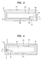
- Fig. 3 is a top view of an antenna element shown in Fig. 1
- Fig. 4 is a bottom view of the antenna element
- Fig. 5 is a characteristic diagram showing the reactance of the antenna element according to frequency
- Fig. 6 is a characteristic diagram showing the antenna resistance of the antenna element according to frequency.
- An antenna device is a receiving antenna for digital terrestrial television broadcasting, and is built in an electronic device such as a mobile phone when being used.
- the antenna device mainly includes an antenna element 2 that is provided on one surface of a circuit board 1, a matching circuit section 3 that is provided on the other surface of the circuit board 1, and a transmission line 4 that is connected to a power supply portion P of the antenna element 2 and reaches the matching circuit section 3.
- a ground conductor (ground) 5 having a large width is formed on one surface of the circuit board 1, and the antenna element 2 is placed on and fixed to one side portion of the circuit board 1.
- a tuning circuit (television tuner circuit) 6 is provided on the other surface of the circuit board 1, and the tuning circuit 6 is connected to the antenna element 2 through the matching circuit section 3 (see Fig. 2 ).
- the antenna element 2 includes a thin plate-like dielectric substrate 20, a first belt-like radiation conductor 21 that is provided on the lower surface of the dielectric substrate 20, a second belt-like radiation conductor 22 that is provided on the upper surface of the dielectric substrate 20, and a through-hole 23 that connects the first belt-like radiation conductor 21 with the second belt-like radiation conductor 22.
- Each of the first and second belt-like radiation conductors 21 and 22 is patterned as a belt-like conductor that has a predetermined width and extends in the shape of a loop.
- the first belt-like radiation conductor 21 is formed on the lower surface of the dielectric substrate 20 as a belt-like conductor that has a rectangular shape in a plan view and is discontinuous at one portion thereof.
- a base end portion of the first belt-like radiation conductor 21 is formed of the power supply portion P of the antenna element 2.
- a tip portion 21a of the first belt-like radiation conductor 21 is formed at such a position that a predetermined gap G is formed between the power supply portion P and the tip portion. The tip portion is capacitively coupled to the power supply portion P.
- the first belt-like radiation conductor 21 includes a base end-sided long side portion 21b that linearly extends from the power supply portion P, and a tip-sided long side portion 21c that extends substantially parallel to the base end-sided long side portion 21b.
- the base end-sided long side portion 21b is connected to the through-hole 23 in the vicinity of the power supply portion P.
- the power supply portion P is bonded by soldering to the transmission line 4, which is provided on the circuit board 1. Accordingly, the matching circuit section 3 and the tuning circuit 6 shown in Fig. 2 are connected to the power supply portion P through the transmission line 4.
- the second belt-like radiation conductor 22 is formed on the upper surface of the dielectric substrate 20 as a belt-like conductor that has a U shape similar to the shape of the first belt-like radiation conductor 21 in a plan view.
- the first and second belt-like radiation conductors 21 and 22 substantially face each other with the dielectric substrate 20 therebetween. That is, the second belt-like radiation conductor 22 includes a base end-sided long side portion 22b that linearly extends from the base end portion 22a of the second belt-like radiation conductor, and a tip-sided long side portion 22c that extends substantially parallel to the base end-sided long side portion 22b.
- the base end portion 22a is connected to the through-hole 23, and the tip portion 22d of the tip-sided long side portion 22c is formed of an open end. Further, the base end-sided long side portion 22b of the second belt-like radiation conductor 22 is formed directly above the base end-sided long side portion 21b of the first belt-like radiation conductor 21, and the long side portions 21b and 22b face each other. Furthermore, the tip-sided long side portion 22c of the second belt-like radiation conductor 22 is formed at a position that is offset from the position directly above the tip-sided long side portion 21c of the first belt-like radiation conductor 21 toward the base end-sided long side portion 22b by the width of the tip-sided long side portion.
- the matching circuit section 3 includes variable capacitance elements 30 and 31, inductance elements 32 and 33, resistance elements 34 and 35, and a capacitor 36.
- the variable capacitance elements 30 and 31 are varactor diodes (varicap diodes), and are connected to each other in series in opposite directions.
- the inductance element 32 is connected to the variable capacitance element 31 in series, and the inductance element 33 is provided between the inductance element 32 and a ground line (not shown).
- the resistance element 34 is provided between an anode of the variable capacitance element 30 and a ground line (not shown), and the resistance element 35 is connected to cathodes of the variable capacitance elements 30 and 31.
- the matching circuit section 3 is connected to the power supply portion P of the antenna element 2 in series through the transmission line 4, and the input impedance and characteristic impedance are matched with each other by the variable capacitance elements 30 and 31 and the inductance elements 32 and 33. Further, the variable capacitance elements 30 and 31 and the inductance elements 32 and 33 are connected via the capacitor 36 to a transmission line 7 for a high-frequency signal (RF signal).
- the resistance element 35 is provided between the transmission line 7 and a connection point that is formed between the variable capacitance elements 30 and 31. Further, a tuning voltage Vt, which forms a reverse voltage, is applied to the variable capacitance elements 30 and 31 through the resistance element 35, so that the resonant frequency of the antenna element 2 is changed.
- the transmission line 7 connects the matching circuit section 3 with the tuning circuit 6.
- a PWM (pulse-width modulation) signal or a power supply voltage is applied to a bias circuit that is included in the tuning circuit 6, so that the tuning voltage Vt is generated. Further, if the tuning voltage Vt is increased, the capacitance values of the variable capacitance elements 30 and 31 are decreased. If the tuning voltage Vt is decreased, the capacitance values of the variable capacitance elements 30 and 31 are increased. Accordingly, if the capacitance values of the variable capacitance elements 30 and 31 are controlled by changing the tuning voltage Vt, it may be possible to variably tune the resonant frequency of the antenna element 2 to the frequency of the radio waves to be received (the signal waves of digital terrestrial television broadcasting).
- the resonant frequency of the antenna element 2 is previously set to f1 that is higher than the frequency band (470 to 770 MHz) of the radio waves to be received, and the resonant frequency is changed by the connecting of the matching circuit section 3 to the power supply portion P of the antenna element 2 in series.
- the resonant frequency is lowered to f2, which is lower than 470 MHz, by the loading of the inductance element 32.
- the resonant frequency is shifted to a higher frequency by the loading of the variable capacitance elements 30 and 31.
- the shift amount is small.
- the shift amount is increased. Accordingly, if the tuning voltage Vt is decreased so that the value C of the resultant capacitance is set to its maximum value in the specified range, it may be possible to set the resonant frequency to 470 MHz. In contrast, if the tuning voltage Vt is increased so that the value C of the resultant capacitance is set to its minimum value in the specified range, it may be possible to set the resonant frequency to 770 MHz. That is, it may be possible to set the resonant frequency of the antenna element 2 to an appropriate value in the range of 470 to 770 MHz by controlling the tuning voltage Vt.
- the first and second belt-like radiation conductors 21 and 22 which have substantially the same shape, are each provided on the lower and upper surfaces of the dielectric substrate 20 of the antenna element 2.
- the pair of belt-like radiation conductors 21 and 22 extends as so to have a positional relationship where the belt-like radiation conductors substantially face each other through the dielectric substrate 20.
- the antenna device since the current flows through the first and second belt-like radiation conductors 21 and 22 in the same direction, it may be possible to make the antenna device thinner by reducing the thickness of the dielectric substrate 20 without the loss of the intensity of the radiation electric field.
- the antenna element 2 includes the first and second belt-like radiation conductors 21 and 22 that are formed by patterning on the upper and lower surfaces of the dielectric substrate 20, it may be possible to manufacture the antenna device at a lower cost in comparison to the case where the radiation conductors are formed by patterning in a spiral shape on the surface of a columnar base.
- the second belt-like radiation conductor 22 is added to the first belt-like radiation conductor 21 which includes the power supply portion P, so that the antenna resistance of the antenna element 2 is increased. Accordingly, it may be possible to suppress the match loss of energy that is caused by the mismatch of impedance. That is, an antenna element, which includes only the first belt-like radiation conductor 21 without the second belt-like radiation conductor 22, is manufactured as Comparative Example. Then, the antenna resistance of the antenna element is measured. When the frequency was 470 MHz, the antenna resistance of the antenna element was 3. 6 ⁇ . When the frequency was 770 MHz, the antenna resistance of the antenna element was 7.4 Q.
- an antenna device which includes the antenna element 2 provided on the circuit board 1, is suitable as a built-in antenna that is thin and has a high gain.
- the tip-sided long side portion 22c of the second belt-like radiation conductor 22 is slightly offset from the position directly above the tip-sided long side portion 21c of the first belt-like radiation conductor 21 toward the base end-sided long side portion 22b, and the offset distance thereof is substantially equal to the width of the long side portion 21c or 22c.
- the degree of electromagnetic coupling between the tip-sided long side portion 21c and the tip-sided long side portion 22c facing the tip-sided long side portion 21c becomes weaker. Accordingly, the capacitive reactance is gently changed according to frequency as comparison to when the long side portions 21c and 22c face each other at an offset distance of 0.
- the broken-line curve is the reactance curve of the antenna element (Comparative Example) when the tip-sided long side portion 22c is formed directly above the tip-sided long side portion 21c and an offset distance is 0, and the solid-line curve gentler than the broken-line curve is the reactance curve of the antenna element 2 (this embodiment).
- the same reactance curve as the solid-line curve of Fig. 5 may be obtained.
- the tip-sided long side portion 22c is offset toward the base end-sided long side portion 22b like in this embodiment, the size of the antenna element 2 may be reduced. Accordingly, it is preferable that the tip-sided long side portion is offset toward the base end-sided long side portion.
- the offset distance of the tip-sided long side portion 22c may be set to be smaller or larger than the width of the tip-sided long side portion 21c.
- the tip-sided long side portion 22c is excessively offset toward the base end-sided long side portion 22b, the radiation electric field is apt to be cancelled. Accordingly, it is not preferable that the tip-sided long side portion be excessively offset toward the base end-sided long side portion.
- a predetermined gap G is formed between the power supply portion P and the tip portion 21a of the first belt-like radiation conductor 21 so that the tip portion is capacitively coupled to the power supply portion P. Accordingly, the reduction of the size of the antenna element is achieved without the addition of parts. That is, a capacitance element such as a chip capacitor may be provided between the power supply portion P and the tip portion 21a of the first belt-like radiation conductor 21.
- a predetermined gap G is formed so that the tip portion 21a is capacitively coupled to the power supply portion P like in this embodiment, the structure may be simplified, so that cost may be reduced.
- the gap G between the tip portion 21a and the power supply portion P is set to 0.5 mm in this embodiment, and the antenna resistance of the antenna element 2 is changed along the solid-line curve of Fig. 6 in accordance with frequency.
- the broken-line curve of Fig. 6 represents the antenna resistance according to the frequency when the gap G is set to 1.0 mm (Comparative Example).
- a low-frequency band is a band where the antenna resistance is apt to be lacking.
- the gap G is set so that the antenna resistance is increased in a low-frequency band like in this embodiment, the impedance is apt to be matched in a low-frequency band, so that it may be possible to improve the performance of the antenna device. Meanwhile, even though the gap G may be set to be even smaller (about 0.3 mm), the change of antenna resistance according to the frequency is substantially the same as that in this embodiment.
Landscapes
- Engineering & Computer Science (AREA)
- Computer Networks & Wireless Communication (AREA)
- Details Of Aerials (AREA)
Abstract
An antenna device includes a first belt-like radiation conductor (21) and a second belt-like radiation conductor (22). The first belt-like radiation conductor (21) extends from a power supply portion (P) in the shape of a loop, and a tip portion (21a) of the first belt-like radiation conductor (21) is capacitively coupled to the power supply portion (P). The second belt-like radiation conductor (22) substantially faces the first belt-like radiation conductor (21) over the entire length thereof through a dielectric layer (20). The power supply portion (P) is connected to a tuning circuit (6). One end of the second belt-like radiation conductor (22) is connected to the first belt-like radiation conductor (21) in the vicinity of the power supply portion (P), and the other end of the second belt-like radiation conductor (22) is formed of an open end.
Description
- The present invention contains subject matter related to Japanese Patent Application No.
2008-163535 - The present invention relates to a small antenna device that is suitable for viewing television broadcasting and includes a power supply portion connected to a tuning circuit.
- From the past, there has been known a chip-shaped antenna device that operates as a monopole helical antenna by forming radiation conductors, which are formed of spiral conductor patterns, on the surface of a columnar base made of a dielectric material (for example, see Japanese Unexamined Patent Application Publication No.
2003-142928 - Meanwhile, in the above-mentioned antenna device in the related art where a radiation conductor is formed in a spiral shape on the surface of a columnar base, the direction of current flowing through the radiation conductor that is formed on the upper surface of the columnar base is substantially opposite to the direction of current flowing through the radiation conductor that is formed on the lower surface of the columnar base. Accordingly, if the columnar base is made thin and the radiation conductor formed on the upper surface of the columnar base is close to the radiation conductor formed on the lower surface of the columnar base, an amount of the radiation electric field is cancelled and the antenna gain is extremely degraded. For this reason, it is necessary for this kind of antenna device in the related art to require a certain thickness for the columnar base, which will interferes with the reduction in the thickness of the entire device.
- An advantage of some aspects of the invention is to provide an antenna device at low cost which is suitable as a thin built-in antenna.
- According to an aspect of the invention, an antenna device includes a first belt-like radiation conductor and a second belt-like radiation conductor. The first belt-like radiation conductor extends from a power supply portion in the shape of a loop, and a tip portion of the first belt-like radiation conductor is capacitively coupled to the power supply portion. The second belt-like radiation conductor substantially faces the first belt-like radiation conductor over the entire length thereof through a dielectric layer. The power supply portion is connected to a tuning circuit. One end of the second belt-like radiation conductor is connected to the first belt-like radiation conductor in the vicinity of the power supply portion, and the other end of the second belt-like radiation conductor is formed of an open end.
- In the antenna device having the above-mentioned structure, the current flows through the first and second belt-like radiation conductors, which extend to have a positional relationship where the belt-like radiation conductors substantially face each other through the dielectric layer, in the same direction. Accordingly, it may be possible to make the antenna device thinner by reducing the thickness of the dielectric layer without the loss of the intensity of the radiation electric field. Further, the second belt-like radiation conductor is added to the first belt-like radiation conductor, so that antenna resistance is increased. Accordingly, it may be possible to suppress the match loss of energy that is caused by the mismatch of impedance. For this reason, the antenna device is suitable as a built-in antenna that is thin and has a high gain. Furthermore, the antenna element includes the belt-like radiation conductors formed by patterning on one and the other surfaces of the dielectric layer, which forms the dielectric substrate. Accordingly, it may be possible to manufacture the antenna device at a lower cost in comparison to the case where radiation conductors are formed by patterning in a spiral shape on the surface of a columnar base.
- In the above-mentioned structure, the first belt-like radiation conductor may be provided on one surface of the dielectric layer, the second belt-like radiation conductor may be provided on the other surface of the dielectric layer, and one end of the second belt-like radiation conductor may be connected to the first belt-like radiation conductor through a through-hole in the dielectric layer in the vicinity of the power supply portion. Accordingly, it may be possible to obtain an antenna device of which the thickness is easily reduced by its simple structure. Meanwhile, the first or second belt-like radiation conductor may be provided in an inner layer of a multilayer board.
- Furthermore, in the antenna device having the above-mentioned structure, the first belt-like radiation conductor may include a base end-sided long side portion that linearly extends from the power supply portion and a tip-sided long side portion that extends substantially parallel to the base end-sided long side portion, and a long side portion of the second belt-like radiation conductor, which substantially faces the tip-sided long side portion, may be formed at a position that is offset from the tip-sided long side portion in a plan view in the width direction of the tip-sided long side portion. Accordingly, since the reactance curve becomes gentler, this structure is preferable. That is, the degree of electromagnetic coupling between the tip-sided long side portion of the first belt-like radiation conductor and the long side portion of the second belt-like radiation conductor facing the tip-sided long side portion of the first belt-like radiation conductor becomes weak. Accordingly, capacitive reactance gently changes in accordance with the frequency in comparison to when the long side portions face each other with an offset distance of 0. As a result, impedance is easily matched in the frequency band of the radio waves to be received.
- In this case, the offset distance of the long side portion of the second belt-like radiation conductor may be appropriately selected. However, if the offset distance of the long side portion of the second belt-like radiation conductor is equal to the width of the tip-sided long side portion of the first belt-like radiation conductor, it may be possible to make the reactance curve gentler without any significant changes in the size of the dielectric substrate. Further, if the long side portion of the second belt-like radiation conductor is formed at a position that is offset toward the base end-sided long side portion of the first belt-like radiation conductor in a plan view, it may be possible to make the reactance curve gentler without changing the size of the dielectric substrate.
- In the antenna device having the above-mentioned structure, a capacitance element such as a chip capacitor may be provided between the power supply portion and the tip portion of the first belt-like radiation conductor. Alternatively, a predetermined gap may be formed between the tip portion of the first belt-like radiation conductor and the power supply portion, so that the tip portion of the first belt-like radiation conductor is capacitively coupled to the power supply portion. Accordingly, the structure may be simplified, so that cost may be reduced. For this reason, this structure is preferable.
- In the antenna device having the above-mentioned structure, a matching circuit, which includes variable capacitance elements and inductance elements, may be connected to the power supply portion of the first belt-like radiation conductor in series, and resonant frequency may be changed according to the capacitance values of the variable capacitance elements. In this case, since the frequency band to be used becomes wider, the antenna device is suitable as a receiving antenna and the like for digital terrestrial television broadcasting.
- In the antenna device according to the aspect of the invention, the first and second belt-like radiation conductors substantially face each other through the dielectric layer, and the current flows through the first and second belt-like radiation conductors in the same direction. Accordingly, it may be possible to make the antenna device thinner by reducing the thickness of the dielectric layer without the loss of the intensity of the radiation electric field. Further, the second belt-like radiation conductor is added to the first belt-like radiation conductor, so that antenna resistance is increased. Accordingly, it may be possible to suppress the match loss of energy that is caused by the mismatch of impedance. For this reason, the antenna device is suitable as a built-in antenna that is thin and has a high gain. Furthermore, since the antenna device may include the belt-like radiation conductors formed by patterning on the upper and lower surfaces of the dielectric layer (dielectric substrate), it may be possible to manufacture the antenna device at a lower cost.
-
-
Fig. 1 is a view showing the appearance of an antenna device according to an embodiment of the invention. -
Fig. 2 is an equivalent circuit diagram of the antenna device according to the embodiment. -
Fig. 3 is a top view of an antenna element shown inFig. 1 . -
Fig. 4 is a bottom view of the antenna element. -
Fig. 5 is a characteristic diagram showing the reactance of the antenna element according to frequency. -
Fig. 6 is a characteristic diagram showing the antenna resistance of the antenna element according to frequency. - An embodiment of the invention will be described below with reference to drawings.
Fig. 1 is a view showing the appearance of an antenna device according to an embodiment of the invention,Fig. 2 is an equivalent circuit diagram of the antenna device according to the embodiment,Fig. 3 is a top view of an antenna element shown inFig. 1 ,Fig. 4 is a bottom view of the antenna element,Fig. 5 is a characteristic diagram showing the reactance of the antenna element according to frequency, andFig. 6 is a characteristic diagram showing the antenna resistance of the antenna element according to frequency. - An antenna device according to this'embodiment is a receiving antenna for digital terrestrial television broadcasting, and is built in an electronic device such as a mobile phone when being used. The antenna device mainly includes an
antenna element 2 that is provided on one surface of a circuit board 1, amatching circuit section 3 that is provided on the other surface of the circuit board 1, and atransmission line 4 that is connected to a power supply portion P of theantenna element 2 and reaches thematching circuit section 3. A ground conductor (ground) 5 having a large width is formed on one surface of the circuit board 1, and theantenna element 2 is placed on and fixed to one side portion of the circuit board 1. Further, a tuning circuit (television tuner circuit) 6 is provided on the other surface of the circuit board 1, and thetuning circuit 6 is connected to theantenna element 2 through the matching circuit section 3 (seeFig. 2 ). - The
antenna element 2 includes a thin plate-likedielectric substrate 20, a first belt-like radiation conductor 21 that is provided on the lower surface of thedielectric substrate 20, a second belt-like radiation conductor 22 that is provided on the upper surface of thedielectric substrate 20, and a through-hole 23 that connects the first belt-like radiation conductor 21 with the second belt-like radiation conductor 22. Each of the first and second belt-like radiation conductors - The first belt-
like radiation conductor 21 is formed on the lower surface of thedielectric substrate 20 as a belt-like conductor that has a rectangular shape in a plan view and is discontinuous at one portion thereof. A base end portion of the first belt-like radiation conductor 21 is formed of the power supply portion P of theantenna element 2. Atip portion 21a of the first belt-like radiation conductor 21 is formed at such a position that a predetermined gap G is formed between the power supply portion P and the tip portion. The tip portion is capacitively coupled to the power supply portion P. Further, the first belt-like radiation conductor 21 includes a base end-sidedlong side portion 21b that linearly extends from the power supply portion P, and a tip-sidedlong side portion 21c that extends substantially parallel to the base end-sidedlong side portion 21b. The base end-sidedlong side portion 21b is connected to the through-hole 23 in the vicinity of the power supply portion P. The power supply portion P is bonded by soldering to thetransmission line 4, which is provided on the circuit board 1. Accordingly, thematching circuit section 3 and thetuning circuit 6 shown inFig. 2 are connected to the power supply portion P through thetransmission line 4. - The second belt-
like radiation conductor 22 is formed on the upper surface of thedielectric substrate 20 as a belt-like conductor that has a U shape similar to the shape of the first belt-like radiation conductor 21 in a plan view. The first and second belt-like radiation conductors dielectric substrate 20 therebetween. That is, the second belt-like radiation conductor 22 includes a base end-sidedlong side portion 22b that linearly extends from thebase end portion 22a of the second belt-like radiation conductor, and a tip-sidedlong side portion 22c that extends substantially parallel to the base end-sidedlong side portion 22b. Thebase end portion 22a is connected to the through-hole 23, and thetip portion 22d of the tip-sidedlong side portion 22c is formed of an open end. Further, the base end-sidedlong side portion 22b of the second belt-like radiation conductor 22 is formed directly above the base end-sidedlong side portion 21b of the first belt-like radiation conductor 21, and thelong side portions long side portion 22c of the second belt-like radiation conductor 22 is formed at a position that is offset from the position directly above the tip-sidedlong side portion 21c of the first belt-like radiation conductor 21 toward the base end-sidedlong side portion 22b by the width of the tip-sided long side portion. A short side portion, which is formed between thelong side portions like radiation conductor 22, is formed directly above a short side portion, which is formed between thelong side portions like radiation conductor 21. Accordingly, the second belt-like radiation conductor 22 substantially faces the first belt-like radiation conductor 21 over the entire length thereof. - As shown in
Fig. 2 , thematching circuit section 3 includesvariable capacitance elements inductance elements resistance elements capacitor 36. Thevariable capacitance elements inductance element 32 is connected to thevariable capacitance element 31 in series, and theinductance element 33 is provided between theinductance element 32 and a ground line (not shown). Theresistance element 34 is provided between an anode of thevariable capacitance element 30 and a ground line (not shown), and theresistance element 35 is connected to cathodes of thevariable capacitance elements - The
matching circuit section 3 is connected to the power supply portion P of theantenna element 2 in series through thetransmission line 4, and the input impedance and characteristic impedance are matched with each other by thevariable capacitance elements inductance elements variable capacitance elements inductance elements capacitor 36 to atransmission line 7 for a high-frequency signal (RF signal). Theresistance element 35 is provided between thetransmission line 7 and a connection point that is formed between thevariable capacitance elements variable capacitance elements resistance element 35, so that the resonant frequency of theantenna element 2 is changed. - The
transmission line 7 connects thematching circuit section 3 with thetuning circuit 6. A PWM (pulse-width modulation) signal or a power supply voltage is applied to a bias circuit that is included in thetuning circuit 6, so that the tuning voltage Vt is generated. Further, if the tuning voltage Vt is increased, the capacitance values of thevariable capacitance elements variable capacitance elements variable capacitance elements antenna element 2 to the frequency of the radio waves to be received (the signal waves of digital terrestrial television broadcasting). - Specifically, the resonant frequency of the
antenna element 2 is previously set to f1 that is higher than the frequency band (470 to 770 MHz) of the radio waves to be received, and the resonant frequency is changed by the connecting of thematching circuit section 3 to the power supply portion P of theantenna element 2 in series. For example, the resonant frequency is lowered to f2, which is lower than 470 MHz, by the loading of theinductance element 32. Further, the resonant frequency is shifted to a higher frequency by the loading of thevariable capacitance elements variable capacitance elements antenna element 2 to an appropriate value in the range of 470 to 770 MHz by controlling the tuning voltage Vt. - As described above, in this embodiment, the first and second belt-
like radiation conductors dielectric substrate 20 of theantenna element 2. The pair of belt-like radiation conductors dielectric substrate 20. However, since the current flows through the first and second belt-like radiation conductors dielectric substrate 20 without the loss of the intensity of the radiation electric field. Further, since theantenna element 2 includes the first and second belt-like radiation conductors dielectric substrate 20, it may be possible to manufacture the antenna device at a lower cost in comparison to the case where the radiation conductors are formed by patterning in a spiral shape on the surface of a columnar base. - In addition, the second belt-
like radiation conductor 22 is added to the first belt-like radiation conductor 21 which includes the power supply portion P, so that the antenna resistance of theantenna element 2 is increased. Accordingly, it may be possible to suppress the match loss of energy that is caused by the mismatch of impedance. That is, an antenna element, which includes only the first belt-like radiation conductor 21 without the second belt-like radiation conductor 22, is manufactured as Comparative Example. Then, the antenna resistance of the antenna element is measured. When the frequency was 470 MHz, the antenna resistance of the antenna element was 3. 6 Ω. When the frequency was 770 MHz, the antenna resistance of the antenna element was 7.4 Q. In contrast, when the frequency was 470 MHz, the antenna resistance of theantenna element 2 including the first and second belt-like radiation conductors antenna element 2 provided on the circuit board 1, is suitable as a built-in antenna that is thin and has a high gain. - Further, in the
antenna element 2, the tip-sidedlong side portion 22c of the second belt-like radiation conductor 22 is slightly offset from the position directly above the tip-sidedlong side portion 21c of the first belt-like radiation conductor 21 toward the base end-sidedlong side portion 22b, and the offset distance thereof is substantially equal to the width of thelong side portion long side portion 21c and the tip-sidedlong side portion 22c facing the tip-sidedlong side portion 21c becomes weaker. Accordingly, the capacitive reactance is gently changed according to frequency as comparison to when thelong side portions Fig. 5 , the broken-line curve is the reactance curve of the antenna element (Comparative Example) when the tip-sidedlong side portion 22c is formed directly above the tip-sidedlong side portion 21c and an offset distance is 0, and the solid-line curve gentler than the broken-line curve is the reactance curve of the antenna element 2 (this embodiment). - Meanwhile, even when the tip-sided
long side portion 22c is offset from the position directly above the tip-sidedlong side portion 21c in a direction opposite to the direction of this embodiment (in a direction where the tip-sidedlong side portion 22c becomes distant from the base end-sidedlong side portion 22b), the same reactance curve as the solid-line curve ofFig. 5 may be obtained. However, if the tip-sidedlong side portion 22c is offset toward the base end-sidedlong side portion 22b like in this embodiment, the size of theantenna element 2 may be reduced. Accordingly, it is preferable that the tip-sided long side portion is offset toward the base end-sided long side portion. Further, the offset distance of the tip-sidedlong side portion 22c may be set to be smaller or larger than the width of the tip-sidedlong side portion 21c. However, if the tip-sidedlong side portion 22c is excessively offset toward the base end-sidedlong side portion 22b, the radiation electric field is apt to be cancelled. Accordingly, it is not preferable that the tip-sided long side portion be excessively offset toward the base end-sided long side portion. - Furthermore, in the
antenna element 2, a predetermined gap G is formed between the power supply portion P and thetip portion 21a of the first belt-like radiation conductor 21 so that the tip portion is capacitively coupled to the power supply portion P. Accordingly, the reduction of the size of the antenna element is achieved without the addition of parts. That is, a capacitance element such as a chip capacitor may be provided between the power supply portion P and thetip portion 21a of the first belt-like radiation conductor 21. However, if a predetermined gap G is formed so that thetip portion 21a is capacitively coupled to the power supply portion P like in this embodiment, the structure may be simplified, so that cost may be reduced. - The relationship between the size of the gap G and antenna resistance will be described herein. The gap G between the
tip portion 21a and the power supply portion P is set to 0.5 mm in this embodiment, and the antenna resistance of theantenna element 2 is changed along the solid-line curve ofFig. 6 in accordance with frequency. The broken-line curve ofFig. 6 represents the antenna resistance according to the frequency when the gap G is set to 1.0 mm (Comparative Example). As apparent fromFig. 6 , if the gap G is 0.5 mm, it may be possible to improve antenna resistance in a low-frequency band in comparison to when the gap G is 1.0 mm. A low-frequency band is a band where the antenna resistance is apt to be lacking. Accordingly, if the gap G is set so that the antenna resistance is increased in a low-frequency band like in this embodiment, the impedance is apt to be matched in a low-frequency band, so that it may be possible to improve the performance of the antenna device. Meanwhile, even though the gap G may be set to be even smaller (about 0.3 mm), the change of antenna resistance according to the frequency is substantially the same as that in this embodiment. - It should be understood by those skilled in the art that various modifications, combinations, sub-combinations and alterations may occur depending on the design requirements and other factors insofar as they are within the scope of the appended claims of the equivalents thereof.
Claims (7)
- An antenna device comprising:a first belt-like radiation conductor (21) that extends from a power supply portion (P) in the shape of a loop, a tip portion (21a) of the first belt-like radiation conductor (21) being capacitively coupled to the power supply portion (P); anda second belt-like radiation conductor (22) that substantially faces the first belt-like radiation conductor (21) over the entire length thereof through a dielectric layer (20),characterized in that the power supply portion (P) is connected to a tuning circuit (6), and
one end of the second belt-like radiation conductor (22) is connected to the first belt-like radiation conductor (21) in the vicinity of the power supply portion (P), and the other end of the second belt-like radiation conductor (22) is formed of an open end. - The antenna device according to claim 1,
characterized in that the first belt-like radiation conductor (21) is provided on one surface of the dielectric layer (20), the second belt-like radiation conductor (22) is provided on the other surface of the dielectric layer (20), and one end of the second belt-like radiation conductor (22) is connected to the first belt-like radiation conductor (21) through a through-hole (23) of the dielectric layer (20). - The antenna device according to claim 1 or 2,
characterized in that the first belt-like radiation conductor (21) includes a base end-sided long side portion (21b) that linearly extends from the power supply portion (P), and a tip-sided long side portion (21c) that extends substantially parallel to the base end-sided long side portion (21b), and
a long side portion of the second belt-like radiation conductor (22), which substantially faces the tip-sided long side portion (21c), is formed at a position that is offset from the tip-sided long side portion (21c) in a plan view in a width direction of the tip-sided long side portion (21c). - The antenna device according to claim 3,
characterized in that the offset distance of the long side portion of the second belt-like radiation conductor (22) is equal to the width of the tip-sided long side portion (22c). - The antenna device according to claim 4,
wherein the long side portion of the second belt-like radiation conductor (22) is formed at a position that is offset toward the base end-sided long side portion (22b) in a plan view. - The antenna device according to any one of claims 1 to 5,
characterized in that a predetermined gap (G) is formed between the tip portion (21a) of the first belt-like radiation conductor (21) and the power supply portion (P), so that the tip portion (21a) of the first belt-like radiation conductor (21) is capacitively coupled to the power supply portion (P). - The antenna device according to any one of claims 1 to 6,
characterized in that a matching circuit, which includes variable capacitance elements (30, 31) and inductance elements (32, 33), is connected to the power supply portion (P) in series, and
resonant frequency is changed according to capacitance values of the variable capacitance elements (30, 31).
Applications Claiming Priority (1)
| Application Number | Priority Date | Filing Date | Title |
|---|---|---|---|
| JP2008163535A JP2010004470A (en) | 2008-06-23 | 2008-06-23 | Antenna device |
Publications (1)
| Publication Number | Publication Date |
|---|---|
| EP2139065A1 true EP2139065A1 (en) | 2009-12-30 |
Family
ID=40886573
Family Applications (1)
| Application Number | Title | Priority Date | Filing Date |
|---|---|---|---|
| EP09008166A Withdrawn EP2139065A1 (en) | 2008-06-23 | 2009-06-22 | Antenna device |
Country Status (2)
| Country | Link |
|---|---|
| EP (1) | EP2139065A1 (en) |
| JP (1) | JP2010004470A (en) |
Cited By (7)
| Publication number | Priority date | Publication date | Assignee | Title |
|---|---|---|---|---|
| RU2499354C2 (en) * | 2010-07-06 | 2013-11-20 | Эппл Инк. | Tunable antenna system |
| EP2800202A1 (en) * | 2013-05-02 | 2014-11-05 | Acer Incorporated | Communication device with ground plane antenna |
| CN104157955A (en) * | 2013-05-13 | 2014-11-19 | 宏碁股份有限公司 | Communication device with ground plane antenna |
| US9837715B2 (en) | 2012-04-13 | 2017-12-05 | Denso Corporation | Antenna device |
| CN109378575A (en) * | 2018-10-25 | 2019-02-22 | 歌尔股份有限公司 | Antenna monomer, antenna assembly and electronic equipment |
| CN109742518A (en) * | 2018-12-14 | 2019-05-10 | 惠州Tcl移动通信有限公司 | A kind of antenna platelet, antenna structure and mobile terminal |
| CN112952344A (en) * | 2021-01-27 | 2021-06-11 | 深圳市锐尔觅移动通信有限公司 | Electronic device |
Families Citing this family (3)
| Publication number | Priority date | Publication date | Assignee | Title |
|---|---|---|---|---|
| TWI357687B (en) * | 2008-07-31 | 2012-02-01 | Avermedia Tech Inc | Digital tv antenna |
| US9558132B2 (en) | 2013-08-14 | 2017-01-31 | Intel Corporation | Socket management with reduced latency packet processing |
| JP2020521403A (en) * | 2017-05-23 | 2020-07-16 | ホアウェイ・テクノロジーズ・カンパニー・リミテッド | Antenna assembly |
Citations (8)
| Publication number | Priority date | Publication date | Assignee | Title |
|---|---|---|---|---|
| US20030006937A1 (en) * | 2001-07-05 | 2003-01-09 | Syuichi Sekine | Antenna apparatus |
| JP2003142928A (en) | 2001-11-02 | 2003-05-16 | Matsushita Electric Ind Co Ltd | Tuning antenna |
| EP1324512A2 (en) * | 2001-12-21 | 2003-07-02 | RAI RADIOTELEVISIONE ITALIANA (S.p.A.) | A method and a device for the reception of radio signals, particulary digital, multi-carrier signals |
| DE10292326T5 (en) * | 2001-04-27 | 2004-04-22 | Matsushita Electric Industrial Co. Ltd. | Antenna device and wireless device using them |
| JP2004193875A (en) * | 2002-12-10 | 2004-07-08 | Murata Mfg Co Ltd | Antenna structure and communication apparatus provided with the same |
| WO2005062422A1 (en) * | 2003-12-23 | 2005-07-07 | Macquarie University | Multi-band, broadband, fully-planar antennas |
| EP1617564A1 (en) * | 2003-04-18 | 2006-01-18 | Yokowo Co., Ltd | Variable tuning antenna and mobile wireless device using same |
| JP2008163535A (en) | 2007-01-05 | 2008-07-17 | Nano Carbon Technologies Kk | Carbon fiber composite structure and method for producing carbon fiber composite structure |
-
2008
- 2008-06-23 JP JP2008163535A patent/JP2010004470A/en not_active Withdrawn
-
2009
- 2009-06-22 EP EP09008166A patent/EP2139065A1/en not_active Withdrawn
Patent Citations (8)
| Publication number | Priority date | Publication date | Assignee | Title |
|---|---|---|---|---|
| DE10292326T5 (en) * | 2001-04-27 | 2004-04-22 | Matsushita Electric Industrial Co. Ltd. | Antenna device and wireless device using them |
| US20030006937A1 (en) * | 2001-07-05 | 2003-01-09 | Syuichi Sekine | Antenna apparatus |
| JP2003142928A (en) | 2001-11-02 | 2003-05-16 | Matsushita Electric Ind Co Ltd | Tuning antenna |
| EP1324512A2 (en) * | 2001-12-21 | 2003-07-02 | RAI RADIOTELEVISIONE ITALIANA (S.p.A.) | A method and a device for the reception of radio signals, particulary digital, multi-carrier signals |
| JP2004193875A (en) * | 2002-12-10 | 2004-07-08 | Murata Mfg Co Ltd | Antenna structure and communication apparatus provided with the same |
| EP1617564A1 (en) * | 2003-04-18 | 2006-01-18 | Yokowo Co., Ltd | Variable tuning antenna and mobile wireless device using same |
| WO2005062422A1 (en) * | 2003-12-23 | 2005-07-07 | Macquarie University | Multi-band, broadband, fully-planar antennas |
| JP2008163535A (en) | 2007-01-05 | 2008-07-17 | Nano Carbon Technologies Kk | Carbon fiber composite structure and method for producing carbon fiber composite structure |
Cited By (11)
| Publication number | Priority date | Publication date | Assignee | Title |
|---|---|---|---|---|
| RU2499354C2 (en) * | 2010-07-06 | 2013-11-20 | Эппл Инк. | Tunable antenna system |
| US9837715B2 (en) | 2012-04-13 | 2017-12-05 | Denso Corporation | Antenna device |
| EP2800202A1 (en) * | 2013-05-02 | 2014-11-05 | Acer Incorporated | Communication device with ground plane antenna |
| US9431696B2 (en) | 2013-05-02 | 2016-08-30 | Acer Incorporated | Communication device with ground plane antenna |
| CN104157955A (en) * | 2013-05-13 | 2014-11-19 | 宏碁股份有限公司 | Communication device with ground plane antenna |
| CN104157955B (en) * | 2013-05-13 | 2017-08-04 | 宏碁股份有限公司 | Communication device with ground plane antenna |
| CN109378575A (en) * | 2018-10-25 | 2019-02-22 | 歌尔股份有限公司 | Antenna monomer, antenna assembly and electronic equipment |
| CN109742518A (en) * | 2018-12-14 | 2019-05-10 | 惠州Tcl移动通信有限公司 | A kind of antenna platelet, antenna structure and mobile terminal |
| CN109742518B (en) * | 2018-12-14 | 2020-12-04 | 惠州Tcl移动通信有限公司 | An antenna small board, an antenna structure and a mobile terminal |
| CN112952344A (en) * | 2021-01-27 | 2021-06-11 | 深圳市锐尔觅移动通信有限公司 | Electronic device |
| CN112952344B (en) * | 2021-01-27 | 2024-01-02 | 深圳市锐尔觅移动通信有限公司 | Electronic equipment |
Also Published As
| Publication number | Publication date |
|---|---|
| JP2010004470A (en) | 2010-01-07 |
Similar Documents
| Publication | Publication Date | Title |
|---|---|---|
| US7375695B2 (en) | Antenna and wireless communication device | |
| US9634390B2 (en) | Antenna device | |
| US8094080B2 (en) | Antenna and radio communication apparatus | |
| EP1983605A1 (en) | Antenna device | |
| CN101461092B (en) | Antenna device | |
| US10277192B2 (en) | Phase shifter, impedance matching circuit, and communication terminal apparatus | |
| JP2010004470A (en) | Antenna device | |
| JP2002076750A (en) | Antenna device and radio equipment equipped with it | |
| CN102077416B (en) | An antenna arrangement | |
| JP2007013981A (en) | Internal chip antenna | |
| US8797225B2 (en) | Antenna device and communication terminal apparatus | |
| EP2128924A1 (en) | Antenna apparatus | |
| CN108336479B (en) | Antennas for mobile communication devices | |
| US20240333320A1 (en) | Multi-Band Antenna for use with Limited Size Ground Planes | |
| US6795027B2 (en) | Antenna arrangement | |
| CN107026313A (en) | Antenna for wireless communication module | |
| JP2012060380A (en) | Antenna device | |
| GB2439863A (en) | Antenna structure and radio communication device using the same | |
| WO2013047033A1 (en) | Antenna device and antenna mounting method | |
| JP2008259039A (en) | Antenna device | |
| JP2009044561A (en) | Antenna matching circuit | |
| JP2009296483A (en) | Antenna device | |
| KR102093480B1 (en) | Antenna apparatus | |
| EP2063486A1 (en) | Antenna apparatus | |
| CN120357181A (en) | Radio communication at a first frequency and a second different frequency |
Legal Events
| Date | Code | Title | Description |
|---|---|---|---|
| PUAI | Public reference made under article 153(3) epc to a published international application that has entered the european phase |
Free format text: ORIGINAL CODE: 0009012 |
|
| AK | Designated contracting states |
Kind code of ref document: A1 Designated state(s): AT BE BG CH CY CZ DE DK EE ES FI FR GB GR HR HU IE IS IT LI LT LU LV MC MK MT NL NO PL PT RO SE SI SK TR |
|
| STAA | Information on the status of an ep patent application or granted ep patent |
Free format text: STATUS: THE APPLICATION HAS BEEN WITHDRAWN |
|
| 18W | Application withdrawn |
Effective date: 20100120 |