EP2139035A1 - Flotox-type eeprom and method for manufacturing the same - Google Patents
Flotox-type eeprom and method for manufacturing the same Download PDFInfo
- Publication number
- EP2139035A1 EP2139035A1 EP08740518A EP08740518A EP2139035A1 EP 2139035 A1 EP2139035 A1 EP 2139035A1 EP 08740518 A EP08740518 A EP 08740518A EP 08740518 A EP08740518 A EP 08740518A EP 2139035 A1 EP2139035 A1 EP 2139035A1
- Authority
- EP
- European Patent Office
- Prior art keywords
- region
- channel stopper
- flotox
- tunnel window
- floating gate
- Prior art date
- Legal status (The legal status is an assumption and is not a legal conclusion. Google has not performed a legal analysis and makes no representation as to the accuracy of the status listed.)
- Withdrawn
Links
Images

Classifications
-
- H—ELECTRICITY
- H10—SEMICONDUCTOR DEVICES; ELECTRIC SOLID-STATE DEVICES NOT OTHERWISE PROVIDED FOR
- H10B—ELECTRONIC MEMORY DEVICES
- H10B41/00—Electrically erasable-and-programmable ROM [EEPROM] devices comprising floating gates
- H10B41/30—Electrically erasable-and-programmable ROM [EEPROM] devices comprising floating gates characterised by the memory core region
-
- H—ELECTRICITY
- H10—SEMICONDUCTOR DEVICES; ELECTRIC SOLID-STATE DEVICES NOT OTHERWISE PROVIDED FOR
- H10B—ELECTRONIC MEMORY DEVICES
- H10B41/00—Electrically erasable-and-programmable ROM [EEPROM] devices comprising floating gates
- H10B41/30—Electrically erasable-and-programmable ROM [EEPROM] devices comprising floating gates characterised by the memory core region
- H10B41/35—Electrically erasable-and-programmable ROM [EEPROM] devices comprising floating gates characterised by the memory core region with a cell select transistor, e.g. NAND
-
- H—ELECTRICITY
- H10—SEMICONDUCTOR DEVICES; ELECTRIC SOLID-STATE DEVICES NOT OTHERWISE PROVIDED FOR
- H10D—INORGANIC ELECTRIC SEMICONDUCTOR DEVICES
- H10D30/00—Field-effect transistors [FET]
- H10D30/01—Manufacture or treatment
- H10D30/021—Manufacture or treatment of FETs having insulated gates [IGFET]
- H10D30/0411—Manufacture or treatment of FETs having insulated gates [IGFET] of FETs having floating gates
-
- H—ELECTRICITY
- H10—SEMICONDUCTOR DEVICES; ELECTRIC SOLID-STATE DEVICES NOT OTHERWISE PROVIDED FOR
- H10D—INORGANIC ELECTRIC SEMICONDUCTOR DEVICES
- H10D30/00—Field-effect transistors [FET]
- H10D30/60—Insulated-gate field-effect transistors [IGFET]
- H10D30/68—Floating-gate IGFETs
- H10D30/681—Floating-gate IGFETs having only two programming levels
- H10D30/683—Floating-gate IGFETs having only two programming levels programmed by tunnelling of carriers, e.g. Fowler-Nordheim tunnelling
-
- H—ELECTRICITY
- H10—SEMICONDUCTOR DEVICES; ELECTRIC SOLID-STATE DEVICES NOT OTHERWISE PROVIDED FOR
- H10D—INORGANIC ELECTRIC SEMICONDUCTOR DEVICES
- H10D30/00—Field-effect transistors [FET]
- H10D30/60—Insulated-gate field-effect transistors [IGFET]
- H10D30/68—Floating-gate IGFETs
- H10D30/6891—Floating-gate IGFETs characterised by the shapes, relative sizes or dispositions of the floating gate electrode
-
- H—ELECTRICITY
- H10—SEMICONDUCTOR DEVICES; ELECTRIC SOLID-STATE DEVICES NOT OTHERWISE PROVIDED FOR
- H10D—INORGANIC ELECTRIC SEMICONDUCTOR DEVICES
- H10D64/00—Electrodes of devices having potential barriers
- H10D64/01—Manufacture or treatment
- H10D64/031—Manufacture or treatment of data-storage electrodes
- H10D64/035—Manufacture or treatment of data-storage electrodes comprising conductor-insulator-conductor-insulator-semiconductor structures
Definitions
- the present invention relates to a FLOTOX-TYPE EEPROM.
- the EEPROM has been decreased not only in chip size but also in memory cell size, achieving miniaturization. Particularly, a variety of forming methods for miniaturization as described above have been proposed regarding the tunnel window constituting a path for electrons injected into or extracted from a floating gate as a memory cell.
- the EEPROM must be designed to withstand high voltages of 15 to 20V, for example, because the EEPROM uses FN tunneling current for writing data.
- peripheral circuits also need be designed to withstand high voltages.
- the peripheral circuits and EEPROM are normally formed in the same process flow and hence, are designed to withstand the same voltage level.
- the tunnel window for allowing the FN tunneling current to pass through the EEPROM is formed of a thin oxide film having a thickness of about 70 to 100 ⁇ . It is therefore desired that a junction formed under the tunnel window has a lower breakdown voltage than that of the peripheral circuits such that the tunnel window may not be damaged when an excessive voltage is applied to the tunnel window.
- the breakdown voltage of a drain junction in the EEPROM is also required to withstand high voltages, it is desirable that the breakdown voltage of the drain junction is set to a voltage lower than that of a high breakdown voltage portion of the peripheral circuits. By setting such breakdown voltages, the drain junction is prevented from being subjected to an excessive voltage in cases where, for example, a high voltage is applied to the peripheral circuits for screening early failure. Therefore, the failure of EEPROM or the reduction of number of rewrites can be prevented.
- the present invention has a primary object to provide a FLOTOX-TYPE EEPROM which can prevent a problem that the excessive voltage is applied to the tunnel window to cause failure or to reduce the number of rewrites.
- Another object of the invention is to provide a FLOTOX-TYPE EEPROM wherein the breakdown voltage of the drain junction and the breakdown voltage of the junction formed under the tunnel window are set to a voltage lower than that of the high breakdown voltage portion of the peripheral circuits such that the drain junction and tunnel window are prevented from being subjected to the excessive voltage when the high voltage is applied for screening the peripheral circuits.
- a still another object of the invention is to provide a FLOTOX-TYPE EEPROM which reduces stress on the thin oxide film called the tunnel window by limiting the voltage applied to the oxide film and is increased in the number of rewrites.
- Yet another object of the invention is to provide a manufacture method of FLOTOX-TYPE EEPROM wherein the breakdown voltages of the tunnel window and drain junction can be adjusted by taking simple manufacture steps.
- the FLOTOX-TYPE EEPROM which is formed at a surface layer region of a semiconductor substrate isolated by field oxide films (18) and which comprises a floating gate (11), a drain region (14) and a tunnel window (12) through which electrons pass during injection from the drain region into the floating gate or extraction from the floating gate, and in which impurity regions (20,25) are formed under the drain region and tunnel window and in which a channel stopper region is formed under the field oxide film, wherein the impurity region (20,25) and the channel stopper region (19) are formed at places spaced apart by a predetermined distance (X,Y) so as not to make contact with each other
- the impurity region (20,25) and the channel stopper region (19) are formed at places spaced apart by the predetermined distance (X,Y) so as not to make contact with each other.
- the configuration is adapted for high breakdown voltage design such that the EEPROM can withstand high voltages of 15 to 20V, for example, applied thereto for passing the FN tunneling current during data writing.
- the EEPROM when an overvoltage is applied to the EEPROM, damage on the tunnel window (12) can be reduced by preventing the application of a voltage above a certain level to the tunnel window (12) and passing the current to the semiconductor substrate (17) based on the level of the applied voltage. Therefore, the EEPROM can be increased in the number of rewrites.
- the FLOTOX-TYPE EEPROM according to the invention may also be configured such that the EEPROM comprises a cell transistor including the floating gate (11) and a select transistor including the drain region (14) and operative to select a floating gate (11) to be subjected to electron injection and extraction, and that in a cross section of a region including the tunnel window (12) and a cross section of the drain region (14) taken in a direction orthogonal to a direction from the cell transistor toward the select transistor, the impurity region (20,25) and the channel stopper region (19) are formed at places spaced apart by a predetermined distance (X,Y).
- the impurity region (20,25) and the channel stopper region (19) are in contact as seen in the above cross section direction and hence, the breakdown voltage thereof is dependent only upon impurity concentration. If the impurity concentration is changed to adjust the breakdown voltage, a field turnover voltage of an isolated area is changed. Therefore, the adjustment of breakdown voltage is difficult and subjected to certain restrictions.
- the above-described configuration is made to ensure that a target voltage is applied to the tunnel window (12) even if the value of program voltage applied by the peripheral circuits is varied.
- the configuration can adjust the damage on the tunnel window (12) and achieve the original goal of EEPROM, namely the increase of the number of rewrites.
- the invention is a manufacture method of the above FLOTOX-TYPE EEPROM which is characterized in that the distance (X,Y) between the impurity region and the channel stopper region (19) is provided by taking steps including: (a) forming the channel stopper region by light exposure and implantation, and (b) forming the impurity region by light exposure and implantation, and that the distance between the impurity region and the channel stopper region is adjusted to the predetermined distance by adjusting dimensions of resists (23) subjected to the light exposure of the above steps (a) and (b).
- the above-described arrangement allows the junction breakdown voltage of the drain region (14) and the junction breakdown voltage of the impurity region under the tunnel window to be easily adjusted by adjusting the dimensions of the resists during the light exposure and the dosages of ions injected during the formation of the channel stopper region and the impurity region.
- the FLOTOX-TYPE EEPROM having the desired junction breakdown voltages can be manufactured.
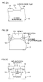
- FIG.1A is a schematic plan view for explaining a configuration of a FLOTOX-TYPE EEPROM according to an embodiment of the invention.
- FIG.1B is a schematic sectional view taken along the line X-X in FIG.1A , showing a cross section structure of the FLOTOX-TYPE EEPROM.
- FIG. 1C is a schematic sectional view taken along the line Y-Y in FIG.1A , showing the cross section structure.
- a floating gate is indicated at 11.
- Indicated at 12 is a tunnel window provided in association with the floating gate 11 and defining a path of electrons to the floating gate 11.
- Indicated at 13 is a select gate provided in correspondence to the floating gate 11.
- a drain region is indicated at 14. The select gate 13 and the drain region 14 belong to a select transistor.
- a control gate laid over the floating gate 11 is indicated at 15, while indicated at 16 is a source.
- the floating gate 11, control gate 15 and source 16 are components of a cell transistor.
- These select transistor and cell transistor are disposed at a region isolated by LOCOS oxide films 18 as field oxide films formed at a surface layer region of a semiconductor substrate 17.
- the semiconductor substrate 17 is a P-type substrate and a P+ channel stopper region 19 is formed under the LOCOS oxide film 18.
- N regions 20,25 as impurity regions are formed under the tunnel window 12 and in the drain region 14.
- the N region 20 under the drain region 14 includes an N- region and an N+ region formed therein.
- This embodiment is characterized in that in a cross section taken in a direction orthogonal to a direction from the cell transistor toward the select transistor, as shown in FIG.1B , the N region 20 formed in the drain region 14 and the channel stopper region 19 formed under the LOCOS oxide film 18 are spaced apart by a predetermined distance X so as not to make contact with each other.
- the embodiment is further characterized in that the N region 25 formed under the tunnel window 12 and the channel stopper region 19 formed under the LOCOS oxide film 18 are spaced apart by a predetermined distance Y.
- the N region 20 formed in the drain region 14 and the channel stopper region 19 are spaced apart by the predetermined distance X thereby making it easy to design the breakdown voltage of the drain junction to be as high as required for the EEPROM within a range lower than a breakdown voltage of a high breakdown voltage portion of peripheral circuits.
- the breakdown voltage of the drain region 14 can be relatively freely set to a desired level by adjusting the distance X between the N region formed in the drain region 14 and the channel stopper region 19 to the predetermined distance. On this occasion, it is desirable to adjust the concentrations of the N region 20 and channel stopper region 19 along with the adjustment of the distance X.
- the N region 25 formed under the tunnel window 12 and the channel stopper region 19 are also formed at places spaced apart by the predetermined distance Y. This allows the breakdown voltage of the tunnel window 12 to be adjusted to a given level.
- the tunnel window can be designed such that when an excessively high voltage is applied to the tunnel window 12, such a high voltage is passed to the semiconductor substrate 17. Hence, the tunnel window 12 is prevented from being subjected to the excessively high voltage.
- FIG.2A to FIG.2C are flow charts each showing a part of a manufacturing process of the FLOTOX-TYPE EEPROM according to another embodiment of the invention.
- the LOCOS oxide films 18 are formed on the surface layer region of the P-type semiconductor substrate 17 by using a common process flow, so as to form an isolated region 22.
- a resist 23 is formed to cover the region 22 and exposed to light.
- a range of the resist to be removed by the light exposure is adjusted such that the resist 23 covering the region 22 may also cover an edge portion of the LOCOS oxide film 18.
- the predetermined distance X (or Y) can be provided between the channel stopper region 19 and the N region 20(25), as will be described hereinlater.
- an implantation step is performed for forming the channel stopper region 19 under a part of the LOCOS oxide film 18 that is not covered by the resist 23.
- Ions injected by the implantation step are, for example, boron (B+).
- the resist 23 is removed after the formation of the channel stopper region 19.
- an implantation step is performed using the LOCOS oxide film 18 as a resist.
- the injected ions may be, for example, arsenic (As+) or phosphorus (P).
- junction breakdown voltage of the N region 20(25) to be formed can also be adjusted by adjusting the dosage of ions injected in the implantation step shown in FIG.2B and FIG.2C .
- the common manufacturing process of EEPROM is carried out.
- the invention is not limited to the teachings of the embodiments described above and various changes or modifications may be made thereto within the scope of the claims thereof.
Landscapes
- Non-Volatile Memory (AREA)
- Semiconductor Memories (AREA)
Abstract
A FLOTOX-TYPE EEPROM of the invention has a configuration wherein an N region 25 as an impurity region formed under a tunnel window 12 and a channel stopper region 19 formed under a LOCOS oxide film 18 are spaced apart by a predetermined distance Y. Therefore, the tunnel window 12 does not sustain damage if an excessive voltage is applied to the tunnel window 12. As a result, the FLOTOX-TYPE EEPROM is adapted to limit the voltage applied to the tunnel window 12 and to reduce stress on the tunnel window 12 and can achieve an increased number of rewrites.
Description
- The present invention relates to a FLOTOX-TYPE EEPROM.
- Electrically writable and rewritable EEPROMs find extensive applications because it allows on-board rewrite and rewrite in units of pages or bytes. In recent years, therefore, manufacture methods for forming fine tunnel windows on FLOTOX-TYPE EEPROM have been proposed in Patent Documents 1 to 3 and the like.
- Patent Document 1: Japanese Unexamined Patent Application Publication No.
2007-027406 - Patent Document 2: Japanese Unexamined Patent Application Publication No.
2006-028873 - Patent Document 3: Japanese Unexamined Patent Application Publication No.
2005-183763 - The EEPROM has been decreased not only in chip size but also in memory cell size, achieving miniaturization. Particularly, a variety of forming methods for miniaturization as described above have been proposed regarding the tunnel window constituting a path for electrons injected into or extracted from a floating gate as a memory cell.
By the way, the EEPROM must be designed to withstand high voltages of 15 to 20V, for example, because the EEPROM uses FN tunneling current for writing data. Accordingly, peripheral circuits also need be designed to withstand high voltages. The peripheral circuits and EEPROM are normally formed in the same process flow and hence, are designed to withstand the same voltage level. - However, the tunnel window for allowing the FN tunneling current to pass through the EEPROM is formed of a thin oxide film having a thickness of about 70 to 100Å. It is therefore desired that a junction formed under the tunnel window has a lower breakdown voltage than that of the peripheral circuits such that the tunnel window may not be damaged when an excessive voltage is applied to the tunnel window.
- Although a breakdown voltage of a drain junction in the EEPROM is also required to withstand high voltages, it is desirable that the breakdown voltage of the drain junction is set to a voltage lower than that of a high breakdown voltage portion of the peripheral circuits. By setting such breakdown voltages, the drain junction is prevented from being subjected to an excessive voltage in cases where, for example, a high voltage is applied to the peripheral circuits for screening early failure. Therefore, the failure of EEPROM or the reduction of number of rewrites can be prevented.
- In view of the foregoing, the present invention has a primary object to provide a FLOTOX-TYPE EEPROM which can prevent a problem that the excessive voltage is applied to the tunnel window to cause failure or to reduce the number of rewrites.
Another object of the invention is to provide a FLOTOX-TYPE EEPROM wherein the breakdown voltage of the drain junction and the breakdown voltage of the junction formed under the tunnel window are set to a voltage lower than that of the high breakdown voltage portion of the peripheral circuits such that the drain junction and tunnel window are prevented from being subjected to the excessive voltage when the high voltage is applied for screening the peripheral circuits. - A still another object of the invention is to provide a FLOTOX-TYPE EEPROM which reduces stress on the thin oxide film called the tunnel window by limiting the voltage applied to the oxide film and is increased in the number of rewrites.
Yet another object of the invention is to provide a manufacture method of FLOTOX-TYPE EEPROM wherein the breakdown voltages of the tunnel window and drain junction can be adjusted by taking simple manufacture steps. - According to the invention for achieving the above objects, the FLOTOX-TYPE EEPROM which is formed at a surface layer region of a semiconductor substrate isolated by field oxide films (18) and which comprises a floating gate (11), a drain region (14) and a tunnel window (12) through which electrons pass during injection from the drain region into the floating gate or extraction from the floating gate, and in which impurity regions (20,25) are formed under the drain region and tunnel window and in which a channel stopper region is formed under the field oxide film, wherein the impurity region (20,25) and the channel stopper region (19) are formed at places spaced apart by a predetermined distance (X,Y) so as not to make contact with each other
- The alphanumeric characters in parentheses represent corresponding components and the like of an embodiment to be described hereinlater. However, the alphanumeric characters do not mean to limit the scope of the invention. Hereinafter, the same holds for this term.
According to this configuration, the impurity region (20,25) and the channel stopper region (19) are formed at places spaced apart by the predetermined distance (X,Y) so as not to make contact with each other. Thus, the configuration is adapted for high breakdown voltage design such that the EEPROM can withstand high voltages of 15 to 20V, for example, applied thereto for passing the FN tunneling current during data writing. - Furthermore, when an overvoltage is applied to the EEPROM, damage on the tunnel window (12) can be reduced by preventing the application of a voltage above a certain level to the tunnel window (12) and passing the current to the semiconductor substrate (17) based on the level of the applied voltage. Therefore, the EEPROM can be increased in the number of rewrites.
The FLOTOX-TYPE EEPROM according to the invention may also be configured such that the EEPROM comprises a cell transistor including the floating gate (11) and a select transistor including the drain region (14) and operative to select a floating gate (11) to be subjected to electron injection and extraction, and that in a cross section of a region including the tunnel window (12) and a cross section of the drain region (14) taken in a direction orthogonal to a direction from the cell transistor toward the select transistor, the impurity region (20,25) and the channel stopper region (19) are formed at places spaced apart by a predetermined distance (X,Y). - In a conventional EEPROM, the impurity region (20,25) and the channel stopper region (19) are in contact as seen in the above cross section direction and hence, the breakdown voltage thereof is dependent only upon impurity concentration. If the impurity concentration is changed to adjust the breakdown voltage, a field turnover voltage of an isolated area is changed. Therefore, the adjustment of breakdown voltage is difficult and subjected to certain restrictions. However, the above-described configuration is made to ensure that a target voltage is applied to the tunnel window (12) even if the value of program voltage applied by the peripheral circuits is varied. The configuration can adjust the damage on the tunnel window (12) and achieve the original goal of EEPROM, namely the increase of the number of rewrites.
- The invention is a manufacture method of the above FLOTOX-TYPE EEPROM which is characterized in that the distance (X,Y) between the impurity region and the channel stopper region (19) is provided by taking steps including: (a) forming the channel stopper region by light exposure and implantation, and (b) forming the impurity region by light exposure and implantation, and that the distance between the impurity region and the channel stopper region is adjusted to the predetermined distance by adjusting dimensions of resists (23) subjected to the light exposure of the above steps (a) and (b).
- In a case where the channel stopper region (19) and the impurity region (20,25) are formed on the semiconductor substrate (17) isolated by the field oxides (18) formed using a common manufacturing process, the above-described arrangement allows the junction breakdown voltage of the drain region (14) and the junction breakdown voltage of the impurity region under the tunnel window to be easily adjusted by adjusting the dimensions of the resists during the light exposure and the dosages of ions injected during the formation of the channel stopper region and the impurity region. Thus, the FLOTOX-TYPE EEPROM having the desired junction breakdown voltages can be manufactured.
- The above and other objects, features and effects of the present invention will become apparent from the following description of the embodiment thereof made with reference to the accompanying drawings.
-
- [
FIG.1A ] A schematic plan view for explaining a configuration of a FLOTOX-TYPE EEPROM according to an embodiment of the invention. - [
FIG.1B ] A schematic sectional view for explaining the configuration of the FLOTOX-TYPE EEPROM according to the embodiment of the invention. - [
FIG.1C ] A schematic sectional view for explaining the configuration of the FLOTOX-TYPE EEPROM according to the embodiment of the invention. - [
FIG.2A ] A flow chart showing a part of a manufacturing process of the FLOTOX-TYPE EEPROM according to another embodiment of the invention. - [
FIG.2B ] A flow chart showing a part of the manufacturing process of the FLOTOX-TYPE EEPROM according to the embodiment of the invention. - [
FIG.2C ] A flow chart showing a part of the manufacturing process of the FLOTOX-TYPE EEPROM according to the embodiment of the invention. -
- 11:
- Floating gate
- 12:
- Tunnel window
- 13:
- Select gate
- 14:
- Drain
- 17:
- Semiconductor substrate
- 18:
- Field oxide film (LOCOS oxide film)
- 19:
- Channel stopper region
- 20,25:
- Impurity region (N region)
- 23:
- Resist
- An embodiment of the invention will be described in detail as below with reference to the accompanying drawings.
FIG.1A is a schematic plan view for explaining a configuration of a FLOTOX-TYPE EEPROM according to an embodiment of the invention.FIG.1B is a schematic sectional view taken along the line X-X inFIG.1A , showing a cross section structure of the FLOTOX-TYPE EEPROM.FIG. 1C is a schematic sectional view taken along the line Y-Y inFIG.1A , showing the cross section structure.
InFIG.1A, FIG.1B and FIG.1C , a floating gate is indicated at 11. Indicated at 12 is a tunnel window provided in association with the floatinggate 11 and defining a path of electrons to the floatinggate 11. Indicated at 13 is a select gate provided in correspondence to the floatinggate 11. A drain region is indicated at 14. Theselect gate 13 and thedrain region 14 belong to a select transistor. - A control gate laid over the floating
gate 11 is indicated at 15, while indicated at 16 is a source. The floatinggate 11,control gate 15 andsource 16 are components of a cell transistor.
These select transistor and cell transistor are disposed at a region isolated byLOCOS oxide films 18 as field oxide films formed at a surface layer region of asemiconductor substrate 17. In this embodiment, thesemiconductor substrate 17 is a P-type substrate and a P+channel stopper region 19 is formed under theLOCOS oxide film 18. -
N regions tunnel window 12 and in thedrain region 14. It is noted that theN region 20 under thedrain region 14 includes an N- region and an N+ region formed therein.
This embodiment is characterized in that in a cross section taken in a direction orthogonal to a direction from the cell transistor toward the select transistor, as shown inFIG.1B , theN region 20 formed in thedrain region 14 and thechannel stopper region 19 formed under theLOCOS oxide film 18 are spaced apart by a predetermined distance X so as not to make contact with each other. - As shown in
FIG.1C , the embodiment is further characterized in that theN region 25 formed under thetunnel window 12 and thechannel stopper region 19 formed under theLOCOS oxide film 18 are spaced apart by a predetermined distance Y. It is noted that the predetermined distance X and the predetermined distance Y may be X=Y or X≠Y, provided that X≠0 and Y≠0.
In this manner, theN region 20 formed in thedrain region 14 and thechannel stopper region 19 are spaced apart by the predetermined distance X thereby making it easy to design the breakdown voltage of the drain junction to be as high as required for the EEPROM within a range lower than a breakdown voltage of a high breakdown voltage portion of peripheral circuits. In other words, the breakdown voltage of the drain region 14 (drain junction) can be relatively freely set to a desired level by adjusting the distance X between the N region formed in thedrain region 14 and thechannel stopper region 19 to the predetermined distance. On this occasion, it is desirable to adjust the concentrations of theN region 20 andchannel stopper region 19 along with the adjustment of the distance X. - Similarly, the
N region 25 formed under thetunnel window 12 and thechannel stopper region 19 are also formed at places spaced apart by the predetermined distance Y. This allows the breakdown voltage of thetunnel window 12 to be adjusted to a given level. In addition, the tunnel window can be designed such that when an excessively high voltage is applied to thetunnel window 12, such a high voltage is passed to thesemiconductor substrate 17. Hence, thetunnel window 12 is prevented from being subjected to the excessively high voltage. - When the
N region 25 under thetunnel window 12 and thechannel stopper region 19 proximate thereto are formed, the breakdown voltage at a portion of thetunnel window 12 can be set with a certain degree of freedom by adjusting the above distance Y and the concentrations of theregions
FIG.2A to FIG.2C are flow charts each showing a part of a manufacturing process of the FLOTOX-TYPE EEPROM according to another embodiment of the invention. - As shown in
FIG.2A , theLOCOS oxide films 18 are formed on the surface layer region of the P-type semiconductor substrate 17 by using a common process flow, so as to form anisolated region 22.
Subsequently, as shown inFIG.2B , a resist 23 is formed to cover theregion 22 and exposed to light. At this time, a range of the resist to be removed by the light exposure is adjusted such that the resist 23 covering theregion 22 may also cover an edge portion of theLOCOS oxide film 18. Thus, the predetermined distance X (or Y) can be provided between thechannel stopper region 19 and the N region 20(25), as will be described hereinlater. - Subsequently, an implantation step is performed for forming the
channel stopper region 19 under a part of theLOCOS oxide film 18 that is not covered by the resist 23. Ions injected by the implantation step are, for example, boron (B+).
As shown inFIG.2B , the resist 23 is removed after the formation of thechannel stopper region 19. As shown inFIG.2C , an implantation step is performed using theLOCOS oxide film 18 as a resist. The injected ions may be, for example, arsenic (As+) or phosphorus (P). - The junction breakdown voltage of the N region 20(25) to be formed can also be adjusted by adjusting the dosage of ions injected in the implantation step shown in
FIG.2B and FIG.2C .
After the N region 20(25) is formed as shown inFIG.2C , the common manufacturing process of EEPROM is carried out.
The invention is not limited to the teachings of the embodiments described above and various changes or modifications may be made thereto within the scope of the claims thereof. - The present application is based on Japanese Patent Application No.
2007-110663
Claims (3)
- A FLOTOX-TYPE EEPROM which is formed at a surface layer region of a semiconductor substrate isolated by field oxide films and which comprises a floating gate, a drain region and a tunnel window through which electrons pass during injection from the drain region into the floating gate or extraction from the floating gate, and in which impurity regions are formed under the drain region and tunnel window and in which a channel stopper region is formed under the field oxide film,
wherein the impurity region and the channel stopper region are formed at places spaced apart by a predetermined distance so as not to make contact with each other. - The FLOTOX-TYPE EEPROM according to Claim 1, wherein the EEPROM comprises a cell transistor including the floating gate and a select transistor including the drain region and operative to select a floating gate to be subjected to electron injection and extraction,
wherein in a cross section of a region including the tunnel window and a cross section of the drain region taken in a direction orthogonal to a direction from the cell transistor toward the select transistor, the impurity region and the channel stopper region are formed at places spaced apart by a predetermined distance. - A manufacture method of the FLOTOX-TYPE EEPROM according to Claim 1 or 2, wherein the distance between the impurity region and the channel stopper region is provided by taking steps including:(1) forming the channel stopper region by light exposure and implantation, and(2) forming the impurity region by light exposure and implantation,wherein the distance between the impurity region and the channel stopper region is adjusted to the predetermined distance by adjusting dimensions of resists subjected to the light exposure of the above steps (1) and (2).
Applications Claiming Priority (2)
| Application Number | Priority Date | Filing Date | Title |
|---|---|---|---|
| JP2007110663A JP5139712B2 (en) | 2007-04-19 | 2007-04-19 | FLOTOX EEPROM and manufacturing method thereof |
| PCT/JP2008/057442 WO2008129999A1 (en) | 2007-04-19 | 2008-04-16 | Flotox-type eeprom and method for manufacturing the same |
Publications (2)
| Publication Number | Publication Date |
|---|---|
| EP2139035A1 true EP2139035A1 (en) | 2009-12-30 |
| EP2139035A4 EP2139035A4 (en) | 2010-11-03 |
Family
ID=39875527
Family Applications (1)
| Application Number | Title | Priority Date | Filing Date |
|---|---|---|---|
| EP08740518A Withdrawn EP2139035A4 (en) | 2007-04-19 | 2008-04-16 | FLOTOX TYPE EEPROM AND METHOD FOR MANUFACTURING THE SAME |
Country Status (5)
| Country | Link |
|---|---|
| US (1) | US8089116B2 (en) |
| EP (1) | EP2139035A4 (en) |
| JP (1) | JP5139712B2 (en) |
| TW (1) | TW200908236A (en) |
| WO (1) | WO2008129999A1 (en) |
Family Cites Families (11)
| Publication number | Priority date | Publication date | Assignee | Title |
|---|---|---|---|---|
| US5844842A (en) * | 1989-02-06 | 1998-12-01 | Hitachi, Ltd. | Nonvolatile semiconductor memory device |
| JPH02308572A (en) * | 1989-05-23 | 1990-12-21 | Toshiba Corp | Programming of semiconductor memory device |
| JPH0770629B2 (en) * | 1990-03-20 | 1995-07-31 | 株式会社東芝 | Method of manufacturing nonvolatile semiconductor memory device |
| US5424567A (en) * | 1991-05-15 | 1995-06-13 | North American Philips Corporation | Protected programmable transistor with reduced parasitic capacitances and method of fabrication |
| JP2603026B2 (en) * | 1992-04-23 | 1997-04-23 | 株式会社東芝 | Method for manufacturing semiconductor device |
| US5550072A (en) * | 1994-08-30 | 1996-08-27 | National Semiconductor Corporation | Method of fabrication of integrated circuit chip containing EEPROM and capacitor |
| JP3869066B2 (en) * | 1997-03-17 | 2007-01-17 | 旭化成マイクロシステム株式会社 | Nonvolatile semiconductor memory device and manufacturing method thereof |
| FR2778018B1 (en) * | 1998-04-28 | 2000-06-23 | Sgs Thomson Microelectronics | METHOD FOR MANUFACTURING EEPROM DEVICES |
| JP2005183763A (en) * | 2003-12-22 | 2005-07-07 | Toshiba Microelectronics Corp | Manufacturing method of semiconductor device including nonvolatile memory |
| JP2006028873A (en) | 2004-07-15 | 2006-02-02 | Hitachi Constr Mach Co Ltd | Intake device for construction machine |
| JP2007027406A (en) | 2005-07-15 | 2007-02-01 | Oki Electric Ind Co Ltd | Manufacturing method of semiconductor device |
-
2007
- 2007-04-19 JP JP2007110663A patent/JP5139712B2/en active Active
-
2008
- 2008-04-16 WO PCT/JP2008/057442 patent/WO2008129999A1/en not_active Ceased
- 2008-04-16 EP EP08740518A patent/EP2139035A4/en not_active Withdrawn
- 2008-04-16 US US12/596,216 patent/US8089116B2/en active Active
- 2008-04-18 TW TW097114287A patent/TW200908236A/en unknown
Also Published As
| Publication number | Publication date |
|---|---|
| JP2008270483A (en) | 2008-11-06 |
| EP2139035A4 (en) | 2010-11-03 |
| JP5139712B2 (en) | 2013-02-06 |
| WO2008129999A1 (en) | 2008-10-30 |
| US8089116B2 (en) | 2012-01-03 |
| TW200908236A (en) | 2009-02-16 |
| US20100084699A1 (en) | 2010-04-08 |
Similar Documents
| Publication | Publication Date | Title |
|---|---|---|
| US6746906B2 (en) | Transistor with ultra-short gate feature and method of fabricating the same | |
| US6703659B2 (en) | Low voltage programmable and erasable flash EEPROM | |
| US7094652B2 (en) | Semiconductor device and method of manufacturing the same | |
| US20030001195A1 (en) | Non-volatile semiconductor memory having a decreased gate length and manufacturing method thereof | |
| US11177393B2 (en) | Semiconductor device with dual types of zero cost embedded memory | |
| EP0820103A1 (en) | Single polysilicon level flash EEPROM cell and manufacturing process therefor | |
| US20050145924A1 (en) | Source/drain adjust implant | |
| US8089116B2 (en) | FLOTOX-TYPE EEPROM and method for manufacturing the same | |
| US5986302A (en) | Semiconductor memory device | |
| US5196361A (en) | Method of making source junction breakdown for devices with source-side erasing | |
| US6168637B1 (en) | Use of a large angle implant and current structure for eliminating a critical mask in flash memory processing | |
| US6329254B1 (en) | Memory cell of the EEPROM type having its threshold adjusted by implantation, and fabrication method | |
| US4148044A (en) | N-channel memory field effect transistor | |
| US7256449B2 (en) | EEPROM device for increasing a coupling ratio and fabrication method thereof | |
| US20020000605A1 (en) | Method of fabricating high-coupling ratio split gate flash memory cell array | |
| US5838616A (en) | Gate edge aligned EEPROM transistor | |
| US6963105B2 (en) | Flash memory cell structure | |
| KR101103813B1 (en) | Manufacturing Method of Flash Memory Device | |
| US20030100157A1 (en) | Flash memory with protruded floating gate | |
| US6146944A (en) | Large angle implantation to prevent field turn-on under select gate transistor field oxide region for non-volatile memory devices | |
| US20020074590A1 (en) | Non-volatile flash memory cell with asymmetric threshold voltage | |
| EP0730305A1 (en) | High voltage N-channel MOSFET in CMOS-type technology and relating manufacturing process | |
| KR100464664B1 (en) | Well structure of high voltage device | |
| JPH06204490A (en) | Semiconductor non-volatile memory | |
| KR20010063281A (en) | A method of fabricating flash memory devices |
Legal Events
| Date | Code | Title | Description |
|---|---|---|---|
| PUAI | Public reference made under article 153(3) epc to a published international application that has entered the european phase |
Free format text: ORIGINAL CODE: 0009012 |
|
| 17P | Request for examination filed |
Effective date: 20091028 |
|
| AK | Designated contracting states |
Kind code of ref document: A1 Designated state(s): AT BE BG CH CY CZ DE DK EE ES FI FR GB GR HR HU IE IS IT LI LT LU LV MC MT NL NO PL PT RO SE SI SK TR |
|
| DAX | Request for extension of the european patent (deleted) | ||
| A4 | Supplementary search report drawn up and despatched |
Effective date: 20101005 |
|
| STAA | Information on the status of an ep patent application or granted ep patent |
Free format text: STATUS: THE APPLICATION IS DEEMED TO BE WITHDRAWN |
|
| 18D | Application deemed to be withdrawn |
Effective date: 20131101 |