EP2137616B1 - Interface processor - Google Patents
Interface processor Download PDFInfo
- Publication number
- EP2137616B1 EP2137616B1 EP08718712.6A EP08718712A EP2137616B1 EP 2137616 B1 EP2137616 B1 EP 2137616B1 EP 08718712 A EP08718712 A EP 08718712A EP 2137616 B1 EP2137616 B1 EP 2137616B1
- Authority
- EP
- European Patent Office
- Prior art keywords
- thread
- port
- activity
- processor
- scheduler
- Prior art date
- Legal status (The legal status is an assumption and is not a legal conclusion. Google has not performed a legal analysis and makes no representation as to the accuracy of the status listed.)
- Active
Links
- 230000000694 effects Effects 0.000 claims description 109
- 239000013598 vector Substances 0.000 claims description 45
- 238000000034 method Methods 0.000 claims description 13
- 230000001419 dependent effect Effects 0.000 claims description 12
- 239000000725 suspension Substances 0.000 claims description 3
- 239000000872 buffer Substances 0.000 description 17
- SVYBEBLNQGDRHF-UHFFFAOYSA-N 4-amino-N-(5-ethyl-1,3,4-thiadiazol-2-yl)benzenesulfonamide Chemical compound S1C(CC)=NN=C1NS(=O)(=O)C1=CC=C(N)C=C1 SVYBEBLNQGDRHF-UHFFFAOYSA-N 0.000 description 15
- 230000007704 transition Effects 0.000 description 12
- 238000012546 transfer Methods 0.000 description 10
- 238000004891 communication Methods 0.000 description 9
- 230000006870 function Effects 0.000 description 9
- 230000008859 change Effects 0.000 description 7
- 230000035484 reaction time Effects 0.000 description 7
- 230000002093 peripheral effect Effects 0.000 description 6
- 230000004044 response Effects 0.000 description 5
- 238000001514 detection method Methods 0.000 description 4
- 238000010586 diagram Methods 0.000 description 3
- 230000008569 process Effects 0.000 description 3
- 230000000630 rising effect Effects 0.000 description 3
- 238000013459 approach Methods 0.000 description 2
- 230000008901 benefit Effects 0.000 description 2
- 238000012544 monitoring process Methods 0.000 description 2
- 230000003334 potential effect Effects 0.000 description 2
- 238000012545 processing Methods 0.000 description 2
- 230000011664 signaling Effects 0.000 description 2
- 230000002457 bidirectional effect Effects 0.000 description 1
- 238000005094 computer simulation Methods 0.000 description 1
- 238000013461 design Methods 0.000 description 1
- 238000005265 energy consumption Methods 0.000 description 1
- 230000006872 improvement Effects 0.000 description 1
- 238000004519 manufacturing process Methods 0.000 description 1
- 238000002360 preparation method Methods 0.000 description 1
- 230000004043 responsiveness Effects 0.000 description 1
- 239000004065 semiconductor Substances 0.000 description 1
Images


Classifications
-
- G—PHYSICS
- G06—COMPUTING; CALCULATING OR COUNTING
- G06F—ELECTRIC DIGITAL DATA PROCESSING
- G06F9/00—Arrangements for program control, e.g. control units
- G06F9/06—Arrangements for program control, e.g. control units using stored programs, i.e. using an internal store of processing equipment to receive or retain programs
- G06F9/30—Arrangements for executing machine instructions, e.g. instruction decode
- G06F9/38—Concurrent instruction execution, e.g. pipeline, look ahead
- G06F9/3836—Instruction issuing, e.g. dynamic instruction scheduling or out of order instruction execution
- G06F9/3851—Instruction issuing, e.g. dynamic instruction scheduling or out of order instruction execution from multiple instruction streams, e.g. multistreaming
-
- G—PHYSICS
- G06—COMPUTING; CALCULATING OR COUNTING
- G06F—ELECTRIC DIGITAL DATA PROCESSING
- G06F13/00—Interconnection of, or transfer of information or other signals between, memories, input/output devices or central processing units
- G06F13/14—Handling requests for interconnection or transfer
-
- G—PHYSICS
- G06—COMPUTING; CALCULATING OR COUNTING
- G06F—ELECTRIC DIGITAL DATA PROCESSING
- G06F1/00—Details not covered by groups G06F3/00 - G06F13/00 and G06F21/00
- G06F1/26—Power supply means, e.g. regulation thereof
- G06F1/32—Means for saving power
- G06F1/3203—Power management, i.e. event-based initiation of a power-saving mode
- G06F1/3234—Power saving characterised by the action undertaken
- G06F1/3237—Power saving characterised by the action undertaken by disabling clock generation or distribution
-
- G—PHYSICS
- G06—COMPUTING; CALCULATING OR COUNTING
- G06F—ELECTRIC DIGITAL DATA PROCESSING
- G06F1/00—Details not covered by groups G06F3/00 - G06F13/00 and G06F21/00
- G06F1/26—Power supply means, e.g. regulation thereof
- G06F1/32—Means for saving power
- G06F1/3203—Power management, i.e. event-based initiation of a power-saving mode
- G06F1/3234—Power saving characterised by the action undertaken
- G06F1/3287—Power saving characterised by the action undertaken by switching off individual functional units in the computer system
-
- G—PHYSICS
- G06—COMPUTING; CALCULATING OR COUNTING
- G06F—ELECTRIC DIGITAL DATA PROCESSING
- G06F9/00—Arrangements for program control, e.g. control units
- G06F9/06—Arrangements for program control, e.g. control units using stored programs, i.e. using an internal store of processing equipment to receive or retain programs
- G06F9/46—Multiprogramming arrangements
- G06F9/48—Program initiating; Program switching, e.g. by interrupt
- G06F9/4806—Task transfer initiation or dispatching
- G06F9/4812—Task transfer initiation or dispatching by interrupt, e.g. masked
-
- Y—GENERAL TAGGING OF NEW TECHNOLOGICAL DEVELOPMENTS; GENERAL TAGGING OF CROSS-SECTIONAL TECHNOLOGIES SPANNING OVER SEVERAL SECTIONS OF THE IPC; TECHNICAL SUBJECTS COVERED BY FORMER USPC CROSS-REFERENCE ART COLLECTIONS [XRACs] AND DIGESTS
- Y02—TECHNOLOGIES OR APPLICATIONS FOR MITIGATION OR ADAPTATION AGAINST CLIMATE CHANGE
- Y02D—CLIMATE CHANGE MITIGATION TECHNOLOGIES IN INFORMATION AND COMMUNICATION TECHNOLOGIES [ICT], I.E. INFORMATION AND COMMUNICATION TECHNOLOGIES AIMING AT THE REDUCTION OF THEIR OWN ENERGY USE
- Y02D10/00—Energy efficient computing, e.g. low power processors, power management or thermal management
-
- Y—GENERAL TAGGING OF NEW TECHNOLOGICAL DEVELOPMENTS; GENERAL TAGGING OF CROSS-SECTIONAL TECHNOLOGIES SPANNING OVER SEVERAL SECTIONS OF THE IPC; TECHNICAL SUBJECTS COVERED BY FORMER USPC CROSS-REFERENCE ART COLLECTIONS [XRACs] AND DIGESTS
- Y02—TECHNOLOGIES OR APPLICATIONS FOR MITIGATION OR ADAPTATION AGAINST CLIMATE CHANGE
- Y02D—CLIMATE CHANGE MITIGATION TECHNOLOGIES IN INFORMATION AND COMMUNICATION TECHNOLOGIES [ICT], I.E. INFORMATION AND COMMUNICATION TECHNOLOGIES AIMING AT THE REDUCTION OF THEIR OWN ENERGY USE
- Y02D30/00—Reducing energy consumption in communication networks
- Y02D30/50—Reducing energy consumption in communication networks in wire-line communication networks, e.g. low power modes or reduced link rate
Definitions
- the present invention relates to an interface processor, that is a processor which is particularly but not exclusively for interfacing with other processors or external devices.
- processor designers One of the challenges facing processor designers is the handling of an ever-increasing number of external devices which wish to communicate with the processor. Generally this is done by providing some kind of interrupt handling capability for the processor for handling activity arising at ports connected to external devices. Increasingly, more sophisticated interface logic is used at these ports to deal with, for example, multiple external devices per port.
- Interfacing is needed in a wide variety of different contexts.
- One context which is discussed herein by way of a background example is in mobile applications processing.
- FIG. 1 shows an exemplary application of a mobile applications processor 2.
- the applications processor 2 comprises a CPU 4 and a plurality of interface controllers 6 which interface with a plurality of peripheral devices 8.
- the interface controllers include: a memory controller 6a for interfacing with a hard-drive (HDD) 8a and a SDRAM memory 8b; a video controller 6b for interfacing with a camera 8c; a display controller 6c for interfacing with an LCD display 8d; an audio controller 6d for interfacing with a microphone 8e, speaker 8f and headset 8g; and a connectivity controller 6e for interfacing with a keyboard 8h, a Universal Serial Bus (USB) device 8i, a Secure Digital (SD) card 8j, a Multi-Media Card (MMC) 8k, and a Universal Asynchronous Receiver/Transmitter (UART) device 81.
- the interface controllers 6 are typically connected to the CPU 4 via a bus 3.
- the system also comprises a power controller 10 and radio processor 12.
- interface controllers 6 are shown somewhat schematically, but represent generally some kind of dedicated I/O logic or specially configured ports.
- interrupts are used, an external peripheral device sends a signal to inform the processor either that it has data ready to input to the processor or that it requires data from the processor.
- polling the processor continually checks the state of the device to determine whether or not it is ready to supply or accept data.
- ASIC Application Specific Integrated Circuit microcontroller
- FPGA Field Programmable Gate Array
- FPGAs are semiconductor devices that can be configured "in the field" after manufacture.
- a computer is used to model the desired logical functions, for example by drawing a schematic diagram or creating a text file describing the functions.
- the FPGA comprises an array of look-up tables which communicate via statically configured interconnects.
- the computer model is compiled using software provided by the FPGA vendor, which creates a binary file that can be downloaded into the FPGA look-up tables. This allows manufacturers of equipment to tailor the FPGA to meet their own individual needs.
- the interface controllers 6 are implemented as FPGAs. This has the benefit that the manufacturer of the mobile telephone can purchase generic FPGA devices 2 and then configure them on site (i.e. "in the field") to be specific to their desired application.
- the disadvantage of FPGAs however is that they are more expensive, slower and consume more power than ASICs.
- the whole chip 2 could be implemented in FPGA, or the chip 2 could be a general purpose processor with separate FPGA chips connected between the chip 2 and the respective peripherals 8.
- these options would be even more expensive and power-consuming - prohibitively so for most mobile phones and other consumer devices.
- US 2002/0161957 discloses a Java processing environment in which a scheduler is provided for performing thread switching between various application layer threads including application layer threads designated to handle interrupts
- WO 97/44732 discloses a microprocessor including a context file configured to store multiple contexts.
- the microprocessor executes multiple threads, each having its own context.
- the microprocessor is capable of executing at least two threads concurrently, a task and an interrupt service routine, and may execute multiple interrupt service routines.
- a processor comprising: an execution unit arranged to execute multiple threads; a thread scheduler; and a first port operable to generate a first indication dependent on a first activity at the first port; characterised in that: the processor comprises a second port operable to generate a second indication dependent on a second activity at the second port; the processor comprises a respective set of thread registers for representing each of said multiple threads; and the thread scheduler is connected to receive said first and second indications and arranged, based on those indications, to schedule said multiple threads for execution by the execution unit supported by a respective set of thread registers for each of the multiple threads, said scheduling including suspending the execution of a thread until receipt of the respective indication; wherein each of the first activity and the second activity is associated with a respective corresponding first and second one of said multiple threads as represented by a respective set of thread registers; wherein the thread scheduler is arranged to transmit, to an identifier register associated with the first port, a first thread identifier
- the thread scheduler may be arranged to transmit, to an identifier register associated with the second port, a second thread identifier relating to a second thread suspended awaiting the second event; and the second indication may comprise return of the second identifier from the identifier register associated with the second port to the thread scheduler.
- each of the threads is associated with activity at a respective port, and the thread scheduler is connected to suspend the threads pending indications of that activity, then the processor is advantageously "primed" to respond quickly to activity occurring at the ports.
- the present invention thus provides a substantial improvement in applications where fast response to external stimuli is desired. Further, while the thread is suspended, if other threads are still to be scheduled then the thread scheduler can begin to schedule those threads.
- This suspended-thread approach is preferable to the use of interrupts when fast reaction time is required.
- the thread scheduler can prepare to execute a thread in expectance of the associated activity, which as discussed above means the processor is ready to react.
- the execution unit is interrupted by a signal from an external device whilst executing some potentially unrelated code. In the interrupt case, the current program state must be saved before the interrupt can be acted upon. The reaction time using interrupts is therefore much slower. Polling is less energy efficient because of the continual queries and responses required.
- the thread scheduler is adapted to manage the execution of the threads, but when it encounters an instruction within a thread which is conditional on certain activity then the thread scheduler can advantageously "set aside” the thread by passing responsibility for it to the respective port with which it is associated. This also aids reaction time.
- the thread scheduler may be arranged to transmit, upon suspending said first thread, a continuation point vector to a vector register associated with the first port; and the continuation point vector may be returned to the execution unit in dependence on the first activity.
- a continuation point vector identifies a point in the code where execution should be continued upon occurrence of the respective activity. This may advantageously allow additional responsibility for the thread to be transferred to the port, and may free up instruction buffers which need not be kept filled with pending instructions.
- continuation point vectors may allow multiple activities (or events) to be handled per thread.
- the first thread may be associated with activity from a plurality of ports, each operable to generate a respective indication in dependence on that activity;
- the execution unit may be adapted to transmit a plurality of continuation point vectors each to a respective one of said plurality of ports, a respective continuation point vector being returned in dependence on the respective activity;
- the thread scheduler may be adapted to suspend the execution of the first thread until receipt of at least one of the respective indications.
- the processor may be adapted to power down at least one of the execution unit, the thread scheduler and a clock once all thread identifiers of suspended threads have been transmitted to ports.
- the processor may be adapted to power up said at least one of the execution unit, thread scheduler and clock upon return of at least one of the thread identifiers from its respective port.
- At least one of the first and second ports may comprise activity handling logic and be associated with at least one condition register for storing a condition, the activity handling logic being arranged to monitor the activity at the port and to generate said indication in dependence on said activity fulfilling said condition.
- the execution unit may be arranged to transmit a respective condition to each condition register.
- a port event enable flag may be associated with the first port; and the thread scheduler may be adapted to enable said first activity to trigger said scheduling by asserting the port event enable flag, and to disable the first activity from triggering said scheduling by de-asserting the port event enable flag.
- a thread event enable flag may be associated with the first thread; and the thread scheduler may be adapted to enable the first thread to be scheduled in dependence on the first activity by asserting the thread event enable flag, and to disable the first thread from being scheduled in dependence on the first activity by de-asserting the thread event enable flag.
- the thread scheduler may be adapted to suspend execution of the first thread pending a third indication of a third activity from a port whilst at least one of the port event enable flag and the thread event enable flag is de-asserted.
- At least one of the port event enable flag and the thread event enable flag may be de-asserted automatically by occurrence of the first activity.
- a plurality of respective port event enable flags may be associated with each of the plurality of ports associated with the first thread; and the thread scheduler may be arranged to assert the thread enable flag and to subsequently assert said plurality of port event enable flags.
- the processor may comprise program memory connected to the execution unit by a bus, wherein the thread scheduler is connected to receive said indications from each of the first and second ports by at least one connection separate from said bus. This removes the need for bus arbitration in the communication between ports and thread scheduler, thus further improving the reaction time of the processor.
- the processor may comprise a plurality of sets of thread registers, each set of thread registers being allocated to store information relating to a respective one of said multiple threads.
- the processor may comprise at least one channel between at least two of said sets, and the thread scheduler may be adapted to schedule a thread based on activity occurring over said channel.
- the processor may be implemented on a chip. At least one of said first and second ports may be an internal port for communicating with another processor on said chip. At least one of said first and second ports may be an external port for communicating with a device external to said chip. At least one external port may be a pin port for detecting rising or falling signal edges occurring at a pin at the chip's physical boundary. At least one external port may be a data port for handling an instantaneous logic-level of one or more bits at the port.
- the execution unit may be adapted to recognise and execute dedicated instructions for suspending and running threads.
- the thread scheduler may be further adapted to schedule a thread based on an interrupt.
- the thread scheduled based on the interrupt is the first thread, and the interrupt interrupts the first thread whilst suspended.
- the thread scheduler may be adapted to schedule a thread without suspension if an associated activity occurs on or before execution of an instruction within that thread which is dependent on that activity.
- a method of scheduling multiple threads for execution within a processor having a first port and a second port comprising: representing each of multiple threads using a respective set of thread registers for each thread; associating a respective corresponding first thread of a respective first set of thread registers with a first activity at the first port, and associating a respective corresponding second thread of a respective second set of thread registers with a second activity at the second port; generating a first indication at the first port in dependence on the first activity; generating a second indication at the second port in dependence on the second activity; and based on said first and second indications, scheduling the threads for execution supported by the respective sets of thread registers, said scheduling including suspending execution of a thread until receipt of the respective indication; and running the threads by executing them in dependence on said scheduling; wherein the method further comprises transmitting, to an identifier register associated with the first port, a first thread identifier relating to a first thread suspended pending the
- a port for use in the scheduling of multiple threads for execution comprising: activity handling logic arranged to generate an indication dependent on activity at the port, a register for storing information identifying a thread associated with said activity, and a register for storing a condition; wherein the activity handling logic is adapted to transmit the first indication on chip when said activity meets said condition.
- a thread scheduler for scheduling multiple threads for execution within a processor having a first port and a second port, wherein: the thread scheduler is adapted to receive a first indication generated by the first port dependent on a first activity at that first port; the thread scheduler is adapted to receive a second indication generated by the second port dependent on a second activity at that second port; and the thread scheduler is adapted to schedule said multiple threads for execution by the execution unit based on said indications, said scheduling including suspending the execution of a thread until receipt of the respective indication; wherein the first activity and the second activity are each associated with respective corresponding threads; wherein the thread scheduler is arranged to transmit, to an identifier register associated with the first port, a first thread identifier relating to the first thread suspended pending the first activity; and the first indication comprises return of the first identifier from the identifier register associated with the first port to the thread scheduler.
- a mobile terminal having a mobile applications processor, at least one peripheral device, and an interface processor connected between the mobile applications processor and the peripheral device, the interface processor comprising: a first port, second port, thread scheduler, thread registers and execution unit as set out above.
- an array of interconnected processors comprising: a first port operable to generate a first indication dependent on a first activity at the first port; a second port operable to generate a second indication dependent on a second activity at the second port; an execution unit arranged to execute multiple threads; and a thread scheduler connected to receive said indications and arranged to schedule said multiple threads for execution by the execution unit based on said indications, said scheduling including suspending the execution of a thread until receipt of the respective indications; wherein the first activity and the second activity are each associated with respective corresponding threads as set out above; and at least one of said first and second ports connects said at least one processor with another processor in the array.
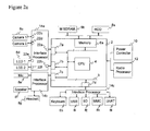
- FIG 2a shows an exemplary application of interface processors in a mobile telephone.
- the mobile applications processor 2 needs to communicate with the plurality of peripheral devices 8.
- the applications processor 2 comprises a bus 3, a CPU 4, and a memory controller 6a for interfacing with a hard-drive (HDD) 8a and a SDRAM memory 8b, as well as a power controller 10 and radio processor 12.
- HDD hard-drive
- SDRAM Secure Digital
- FIG. 1 In place of dedicated controllers 6, the arrangement of Figure 2a allows the CPU 4 to communicate externally via generic ports 7.
- generic ports 7a and 7b are provided for interfacing with cameras 8c and LCD displays 8d; a generic port 7c is provided for interfacing with a microphone 8e, speaker 8f and headset 8g; and a generic port 7d is provided for interfacing with a keyboard 8h, a Universal Serial Bus (USB) device 8i, a Secure Digital (SD) card 8j, an Multi-Media Card (MMC) 8k, and a Universal Asynchronous Receiver/Transmitter (UART) device 81.
- USB Universal Serial Bus
- SD Secure Digital
- MMC Multi-Media Card
- UART Universal Asynchronous Receiver/Transmitter
- interface processors 14a, 14b and 14c are placed at the outputs of the relevant ports 7, with a first interface processor 14a being connected between the image devices 8c-8d and the generic ports 7a-7b, a second interface processor 14b being connected between the audio devices 8e-8g, and a third interface processor 14b being connected between the generic port 7d and the various connectivity devices 8h-8m.
- the ports 7 need only be general purpose ports because the application-specific display, audio and connectivity functions are implemented by the interface processors 14a-14c in a manner to be described later.
- the ports 7 need not use FPGA logic, because the interface processors 14 provide the flexibility and configurability that would otherwise be provided by FPGAs.
- the interface processor 14a has ports 22a and 22b connected to the ports 7a and 7b, and ports 22c, 22d, 22e and 22f connected to the external devices 8c and 8g.
- the interface processors 14b and 14c have similar ports, not shown in Figure 2a .
- the interface processors are typically involved in implementing the specific protocols used to transfer data via the interfaces, re-formatting data including converting it between parallel and serial formats, and possibly higher level functions such as encoding it, compressing it or encrypting it.
- FIG. 2b Another application of an interface processor is as a tile in a multiprocessor chip 202 illustrated in Figure 2b .
- a chip 202 uses a high performance interconnect 204 which supports communication between the processors 14 on the chip 202, and inter-chip links 206 so that systems can easily be constructed from multiple chips.
- Each processor 14 is connected to its inter-chip link 206 and high performance interconnects 204 via ports 22.
- Each interface processor comprises a CPU, memory and communications.
- each processor has hardware support for executing a number of concurrent program threads, each comprising a sequence of instructions, and at least some of which are specifically responsible for handling activity at the ports.
- the hardware support includes:
- each processor can be used to allow communications or input/output to progress together with other pending tasks handled by the processor, and to allow latency hiding in the interconnect by allowing some threads to continue whilst others are suspended pending communication to or from remote interface processors.
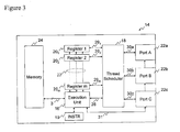
- FIG. 3 shows schematically an exemplary architecture of an interface processor 14 according to one embodiment of the present invention.
- the processor 14 comprises an execution unit 16 for executing threads of instructions under the control of a thread scheduler 18.
- the processor 14 further comprises a Random Access Memory (RAM) 24 for holding program code and other data, and a Read Only Memory (ROM) (not shown) for storing permanent information such as boot code.
- RAM Random Access Memory
- ROM Read Only Memory
- the thread scheduler 18 dynamically selects which thread the execution unit 16 should execute. Conventionally, the function of a thread scheduler would simply be to schedule threads from the program memory in order to keep the processor fully occupied. However, according to the present invention, the scheduling by the thread scheduler 18 is also related to activity at the ports 22. It is noted in this respect that the thread scheduler may be directly coupled to the ports 22 so as to minimise the delay when a thread becomes runable as a result of an input or output activity at the port.
- Each of the m threads under consideration by the thread scheduler 18 is represented by a respective set of thread registers 20 1 ... 20 m in a bank of registers 20, to which the thread scheduler 18 has access.
- Instruction buffers (INSTR) 19 are also provided for temporarily holding instructions fetched from memory 24 before being subsequently issued into the execution unit 16. The details of these registers and buffers are discussed later.
- the thread scheduler 18 maintains a set of n runnable threads, the set being termed "run", from which it takes instructions in turn, preferably in a round-robin manner. When a thread is unable to continue it is suspended by removing it from the run set. The reason for this may be, for example, because the thread is awaiting one or more of the following types of activity:
- a direct hardwired connection 28 is provided between the thread scheduler 18 and the execution unit 16 to allow the thread scheduler 18 to control which thread or threads the execution unit 16 should fetch and execute.
- Direct hardwired paths 30a, 30b, 30c are also provided between the thread scheduler 18 and each of the ports 22; and direct hardwired paths 29 1 ... 29 m are provided between the thread scheduler 18 and each of the registers 20.
- These direct paths preferably provide control paths which allow the thread scheduler to associate a respective thread with one or more of the ports 22, and particularly to return ready indications from the ports when certain activity occurs, allowing the processor to respond quickly to activity or stimuli occurring at the ports 22.
- the operation of the thread scheduler in relation to the ports is discussed below with regard to Figures 4 and 6 .
- the execution unit 16 also has access to each of the ports 22a-22c and each of the registers 20 1 -20 m via direct connections 27 and 31, thus providing a direct link between the core processor, registers, and the external environment.
- these direct paths provide further control paths allowing the execution unit to pass conditions to the ports. This is discussed in further detail below with regard to Figure 4 .
- the direct paths 27 and 31 may also allow data to be input and output directly between the thread registers 20 and the ports 22, thus allowing threads to communicate directly with the external environment. For example, data may be written directly from an external device to one of a thread's operand registers, rather than being written to memory 24 and then subsequently fetched. Conversely, following an operation, data from an operand register may be picked up by the execution unit 16 and sent directly out of a port 22. This improves reaction time significantly.
- direct connection or “direct path” it is meant a connection separate from the connection between the execution unit and the program memory 24.
- the thread scheduler 18 and execution unit 16 have access to data input from ports 22 without that data being stored and then subsequently fetched from memory 24.
- a "direct” connection or path means one which is separate from the bus.
- the ports 22 may also be provided with an additional connection (not shown) with the bus 13.
- a pin port can refer to either a “pin port” or a “data port”.
- a pin port is responsible for detecting individual logical transitions, i.e. rising and falling edges, of a signal occurring at a pin at the processor chip's physical boundary.
- Data ports are "higher level” in that they can handle one or more bits, typically accumulated in an I/O buffer, and typically making up a portion of data such as a word. Instead of detecting rising and falling edges, a data port handles the state or logic level of a bit or bits at a particular instant.
- a data port may be on/off chip, or it may be a port to another processor embedded on the same chip. Note that "pin port” and “data port” may in fact refer to different modes of the same actual port.
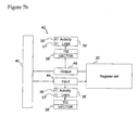
- FIG. 4 shows schematically a port 22 according to a preferred embodiment of the invention.
- the port 22 comprise an I/O-buffer 32 for passing input and output data to and from the processor 14.
- each port 22 comprises activity handling logic 36 for monitoring activity occurring at the port and signalling the occurrence of certain activity by means of at least one ready bit or flag 37.
- the ready flag 37 is preferably signalled to the thread scheduler via direct path 30.
- Potential activity which the port may detect includes:
- the port 22 is provided with a set of registers 38. These comprises a thread identifier (TID) register for storing an identification of the relevant thread, a control (CTRL) register for storing one or more conditions, a continuation point vector (VECTOR) register for storing the position in the program where execution was suspended, and a data (DATA) register for storing any data associated with a condition.
- TID thread identifier
- CRL control
- VECTOR continuation point vector
- DATA data register for storing any data associated with a condition.
- the values TID is written to the registers 38 by the thread scheduler 18 via the direct path 30 (which would be 30a, 30b, 30c in Figure 3 ); and the values VECTOR, CTRL and DATA are written by the execution unit 16 via the direct path 31.
- the TID is returned to the thread scheduler 18 upon detection of the desired activity in order to identify the associated thread.
- the activity logic also comprises an enable flag 39, which is discussed in further detail below.
- registers 38 are shown in Figure 4 as being contained within the port 22, they may in fact be situated elsewhere within the processor 14 and simply associated with the port 22.
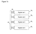
- FIG. 5 shows an exemplary bank of thread registers 20 used to represent the threads.
- the bank 20 comprises a plurality of sets of registers corresponding to respective threads T 1 to T m which are currently under consideration by the thread scheduler 18.
- the state of each thread is represented by eighteen registers: two control registers, four access and twelve operand registers. These are as follows.
- the control registers store information on the status of the thread and for use in controlling execution of the thread. Particularly, the ability of a thread to accept events or interrupts is controlled by information held in the thread status register SR.
- the access registers include a stack pointer used for local variables of procedures, a data pointer normally used for data shared between procedures and a constant pool pointer used to access large constants and procedure entry points.
- the operand registers OP1...OP12 are used by instructions which perform arithmetic and logical operations, access data structures, and call subroutines.
- a number of instruction buffers (INSTR) 19 are also provided for temporarily storing the actual instructions of the thread.
- Each instruction buffer is preferably sixty-four bits long, with each instruction preferably being sixteen bits long, allowing for four instructions per buffer. Instructions are fetched from program memory 24 under control of the thread scheduler 18 and placed temporarily in the instruction buffers 19.
- the execution unit has access to each of the registers 20 and buffers 19. Further, the thread scheduler 18 has access to at least the status register SR for each thread.
- Event refers to a particular type of operation, or to the activity corresponding to that particular type of operation.
- Event based operations are slightly different from basic input-output operations, and work as follows. An event is first set for a thread by transferring a continuation point vector from the execution unit 16 and a thread identifier from the thread scheduler 18 to the VECTOR and TID registers 38 associated with a port 22, preferably via direct paths 31 and 30. An associated condition and condition data may also be written to the CTRL and DATA registers 38 of the port 22. The event is thus set at the port, but not necessarily enabled.
- the port's enable flag 39 must also be asserted, preferably by the thread scheduler 18 via direct path 30. Further, to enable the thread itself to accept events, the thread's event enable (EE) flag in the respective status register SR for the thread must be set to event-enabled. Once the event is thus set and enabled, the thread can be suspending awaiting the event using an event-based wait instruction which acts on the thread scheduler 18. At this point, the current pending instruction may be discarded from the relevant instruction buffer 19. When the event occurs, e.g.
- the occurrence is signalled by the return of the thread identifier and continuation point vector from the port 22 to the thread scheduler 18 and execution unit 16, allowing the instruction at the continuation point vector to be fetched from program memory 24 into an instruction buffer 19 and execution resumed at the appropriate point in the code.
- the thread's EE flag in the respective status register SR may be set to event-disabled to prevent the thread from reacting to events immediately after the occurs.
- the enable flag 39 may be de-asserted as a result of the thread executing instructions when the event occurs.
- the enable flag 39 can be asserted whilst setting up a number of ports in preparation for waiting for an event from one or more of the ports.
- the thread's EE flag may also be set to event-enabled prior to enabling a set of port enable flags and in this case the first port to be enabled which is ready will generate and event causing the current instruction to be discarded and execution to proceed by immediately fetching and executing the instruction at the continuation point vector.
- the advantage of the port's enabling flag 39 and status register EE flag is that the enabling and disabling of events is separated from both the setting up of the events and the suspension of a thread by a wait instruction, allowing different input and output conditions to be readily toggled on and off for a particular thread and/or for various different threads. For example, an event may be left set up at a port 22 even though the event is disabled. Thus events may be re-used by a thread because, although the event has already occurred once, the thread identifier, continuation point vector and condition are still stored in the TID, VECTOR, CTRL and DATA registers 38 of the port 22.
- the port's registers 38 do not need to be re-written, but instead the port's enable flag 39 can simply be reasserted and/or the EE flag in the status register SR for a thread can be re-set to event-enabled. A further wait instruction will then suspend the thread pending a re-occurrence of the same event.
- continuation point vectors allows multiple events to be enabled per thread. That is, a given thread can set up one event at one port 22a by transferring a continuation point vector to that port, set up another event at another port 22b by transferring a different continuation point vector to that other port, and so forth.
- the thread can also enable and disable the various events individually by separately asserting or de-asserting the different enable flags 39 for each respective port. A wait instruction will then cause the thread to be suspended awaiting any enabled event.
- the thread scheduler 18 does not transmit a continuation point vector to the VECTOR register, and does not use the port's enable flag 39 or the EE flag in the status register SR. Instead, the pending instruction is simply left in an instruction buffer 19, and if necessary execution is simply paused pending either an input or the availability of the port for output, as indicated by the ready flag 37.
- only the TID register may be required for scheduling according to a basic I/O.
- a basic I/O may or may not use a condition in the CTRL and DATA registers. If such a condition is not used, the I/O will simply be completed as soon as the port is ready.
- a thread may of course subsequently perform a basic I/O operation.
- a thread may subsequently include an event operation. Any such chain of events and I/Os may be included in a thread.
- a basic I/O operation may be interleaved between two event-based wait operations while the event is disabled (i.e. while the port's enable flag 39 and/or the status register's EE flag is de-asserted) but while the event vector and condition are still left set in the registers 38.
- the event may be disabled following completion of a first event-based wait operation, a basic I/O subsequently performed using the same port, and then the same event re-enabled for use in a second event-based wait operation.
- the basic I/O operation pauses and un-pauses the thread but does not effect the port's enable flag 39 or the EE flag in the status register, nor transfer control to the event vector.
- step 100 the execution unit 16 begins execution of a first and a second thread under the direction of the thread scheduler 18.
- the thread scheduler encounters a portion of code within the first thread which is conditional on an event, for example the receipt of some particular signal at the port 22a.
- the thread scheduler sends the thread identifier (TID) of the first thread to the Port 22a, along with a continuation point vector (VECTOR) specifying at what point in the program thread execution should be continued once the event is detected, and also any required condition control information (CTRL) and associated data (DATA).
- CTRL condition control information
- DATA data may be the value of the signal which the instruction is expecting to receive at the port.
- the thread scheduler may also set the enable flag 39 of the first port and set the status register SR of the first thread to event-enabled.
- the port 22a receives this information from the thread scheduler 18.
- the thread scheduler 18 suspends execution of the first thread.
- the port 22a begins to monitor the activity at that port.
- the thread scheduler 18 determines that the second thread is still outstanding and the execution unit 16 continues execution of the second thread under the direction of the thread scheduler 18.
- the thread scheduler 18 encounters a portion of code which is conditional on an event.
- the thread scheduler 18 sends the thread identifier, along with the continuation point vector and any other required condition information, to the port 22b.
- the thread scheduler may also set the enable flag 39 of the second port and set the second status register for the second thread to event-enabled.
- the port 22b receives this information.
- the thread scheduler suspends execution of the second thread.
- the port 22b begins to monitor the activity occurring at that port.
- the thread scheduler determines that there are currently no more outstanding threads to be scheduled and the system powers down all components except for the ports 22a and 22b.
- the port 22a detects the relevant event, for example the receipt of the signal stored in the DATA register, and consequently returns the thread identifier (TID) and continuation point vector (VECTOR) (as well as setting the status register of the first thread to event-disabled).
- the thread scheduler 18 receives the returned identifier. Now that execution can continue, at step 130 the system powers up again.
- the execution unit 16 completes the execution of the first thread under the direction of the thread scheduler 18.
- the port 22b detects the relevant event for the second thread and returns its thread identifier and continuation point vector (as well as setting the status register of the second thread to event-disabled).
- the thread scheduler 18 receives the returned information, and at step 138 the execution unit 16 completes the execution of the second thread under the control of the thread scheduler 18. Note that there could be an additional powering down step between steps 134 and 136.
- the principle of the invention can also be extended to communication between threads, or more accurately between the thread register sets 20 which store information representing the threads.
- the thread register sets 20 which store information representing the threads.
- Each of the thread register sets is connected to each of the other sets by an interconnect system 40, which is operable to establish at least one channel for transferring data directly between at least two of the thread register sets 20.
- Channels are preferably used to transfer data to and from the operand registers OP, but could in principle be used to transfer information to or from other types of register such as a status register SR.
- the thread scheduler 18 can schedule threads based on activity occurring over channels in a similar manner as discussed in relation to ports above.
- each of the channel ends 42 resembles a pair of ports, with an input buffer 44 and an output buffer 46.
- each channel input buffer 44 and output buffer 46 may have activity handling logic 36' for monitoring activity occurring over a channel and signalling the occurrence of certain activity by means of at least one ready flag 37'.
- Potential activity which the channel end may detect includes: that data has been input to the channel, or that the channel has become available for output. If an output instruction is executed when the channel is too full to take the data then the thread which executed the instruction is paused, and is restarted when there is enough room in the channel for the instruction to successfully complete. Likewise, when an instruction is executed and there is not enough data available then the thread is paused, and will be restarted when enough data becomes available.
- each channel end is associated with registers 38'.
- registers 38' comprise a thread identifier (TID) register for storing an identification of the relevant thread, and a continuation point vector (VECTOR) register for storing the position in the program where execution should resume upon occurrence of an event.
- TID thread identifier
- VECTOR continuation point vector
- the VECTOR register allows the channel to generate events and interrupts.
- the channel end also has an enable flag 39' to enable the channel to generate events.
- the channel ends 42 may not be provided with CTRL and DATA registers.
- the same channel ends 42 may also be used to communicate data from the thread registers to the external environment via the ports 22. That is, the execution unit 16 may pick up the contents of a register 20 via a channel end 42 and pass it directly out via a port 22; and conversely, the execution unit 16 may also receive input from a port 22 and transfer it directly to a register 20 via a channel end 42.
- a channel can also be established between those processors.
- each processor may interface with a system interconnect via a number of bidirectional physical links 204 which allow simultaneous connection with other processors.
- the interface processor can support several programming approaches due to its thread-based structure. It can be treated as a single conventional processor performing standard input and output, or it can be programmed as part of a parallel array of hundreds of communicating components.
- An instruction set is provided which supports these options.
- the instruction set includes special instructions which support initialisation, termination, starting and stopping threads and provide input/output communication.
- the input and output instructions allow very fast communications with external devices. They support high-speed, low-latency input and output and high-level concurrent programming techniques. Their application therein to handling port activity is discussed more fully in the following, which describes example instructions that can be used to implement the present invention. Resources are firstly reserved for a thread using a GETR instruction specifying the type of resource required, and can be freed again using a FREER instruction.
- Ports can be used in input or output mode.
- input mode a condition can be used to filter the data passed to the thread.
- a port can be used to generate events or interrupts when data becomes available as described below. This allows a thread to monitor several ports, only servicing those that are ready.
- Input and output instructions, IN and OUT can then be used to transfer of data to and from ports once ready.
- the INSHR instruction shifts the contents of a register right by n bits, filling the left-most n bits with the data input from the n-bit port.
- the OUTSHR instruction outputs the n least significant bits of data to the n-bit port and shifts the contents of a register right by n bits.
- OUTSHR port s port ⁇ s[bits 0 for width(port)]; output from s ⁇ s >> width(port) port and shift INSHR port, s s ⁇ s >> width(d); shift and input port ⁇ s[bits (bitsperword - width(d)) for width(d)] from port where the " ⁇ " represents an input and the " ⁇ " represents an output.
- a port must be configured before it can be used. It is configured using the SETC instruction which is used to define several independent settings of the port. Each of these has a default mode and need only be configured if a different mode is needed. SETC port, mode port[ctrl] ⁇ mode set port control
- the DRIVE, PULLDOWN and PULLUP modes are only relevant when the port direction is OUT.
- the TRANSITION condition is only relevant for 1 bit ports and the GR and LS conditions are only relevant for ports with more than one bit.
- Each port has a ready bit 37 which is used to control the flow of data through the port, and defines whether the port is able to complete input or output instructions.
- the ready bit is set in different ways depending on the port configuration. The ready bit is cleared when any of the SETC, SETD or SETV instructions are executed.
- a port in input mode can be configured to perform conditional input.
- the condition filters the input data so that only data which meets the condition is returned to the program.
- the IN and INSHR instructions will only complete when the port is ready.
- executing an input instruction on a port which is not ready will pause the thread.
- the port sets its ready bit which is signalled to the thread scheduler. The thread resumes and re-executes the input instruction. This time the port is ready, the data is returned and the ready bit 37 is cleared.
- a port ready bit Once a port ready bit is set, the data value which satisfied the condition is captured so that the software gets the value which met the condition even if the value on the port has subsequently changed.
- the ready bit When an IN or INSHR instruction is executed and the ready bit is set then the data is returned and the ready bit cleared. If the ready bit is not set then the thread is paused until the ready bit is set. If a condition is set then the data is compared against the condition and the ready bit is only set when the condition is met.
- the ready bit When the OUT or OUTSHR instruction is executed if the ready bit is clear then the data is taken by the port and the ready bit is set. If the ready bit is set then the thread is paused until it is cleared by the port.
- two channel ends need to be allocated, one for each tread. This is done using a GETR CHAN instruction.
- the two threads can then use the resource identifiers to transfer a data word using output and input instructions:
- Events and interrupts allow resources (ports and channels) to automatically transfer control to a predefined event handler.
- the ability of a thread to accept events or interrupts is controlled by information held in the thread status register SR (see Figure 4 ), and may be explicitly controlled using TSE and TSD instructions. This information comprises an event enable flag (EE) and an interrupt enable flag (IE).
- EE event enable flag
- IE interrupt enable flag
- the operand of these instructions should be one of: EE to enable or disable events IE to enable or disable interrupts
- Events are handled in the same scope in which they were set up. Hence, on an event all the thread's state is valid, allowing the thread to respond rapidly to the event. The thread can perform input and output operations using the the port which gave rise to an event whilst leaving some or all of the event information unchanged. This allows the thread to complete handling an event and immediately wait for another similar event.
- the program location of the event handler must be set prior to enabling the event using the SETV instruction. Ports have conditions which determine when they will generate an event; these are set using the SETC and SETD instructions. Channels are considered ready as soon as they contain enough data or have room to accept data for output.
- Event generation by a specific port or channel can be enabled using an event enable unconditional (EEU) instruction and disabled using an event disable unconditional (EDU) instruction.
- EEU event enable unconditional
- EET event enable true
- EEF event enable false
- EET event enable true
- EEF event enable false
- SETV port v port[vector] ⁇ v set event vector SETD port, d port[data] ⁇ d set event data SETC port, c port[ctrl] ⁇ c set event control EET port, b port[enable] ⁇ b; port[tid] ⁇ thread event enable true EEF port, b port[enable] ⁇ ⁇ b; port[tid] ⁇ thread eventenable false EDU port port[enable] ⁇ false; port[tid] ⁇ thread event disable EEU port port[enable] ⁇ true; port[tid] ⁇ thread event enable
- a thread can use a WAITEU instruction to wait for at least one event. This may result in an event taking place immediately with control being transferred to the event handler specified by the corresponding event vector with events disabled by clearing the EE (event enable) flag. Alternatively the thread may be suspended until an event takes place - in this case the EE flag will be cleared when the event takes place, and the thread resumes execution.
- EE event enable
- conditional forms of the event wait instruction are provided.
- the WAITET instruction waits only if its condition operand is true, and the WAITEF waits only if its condition operand is false.
- All of the events which have been enabled by a thread can be disabled using a single CLRE instruction. This disables event generation in all of the ports which have had events enabled by the thread.
- the CLRE instruction also clears the event-enabled status in the thread's status register.
- the TSE EE instruction can be used to enable events on a thread first before subsequently starting to enable the ports and/or channels and using one of the event wait instructions. This way, the processor can scan through the resources in priority order. This may cause an event to be handled immediately as soon as it is enabled.
- An interrupt could interrupt a thread whilst suspended awaiting an event.
- the following shows example code for inputting an 8-bit byte serially from a pin.
- Each bit of data is input from a first port when a signal received at a second port from an external clock changes from 0 to 1 to indicate that the data should be taken.
- the operation looks like this:
- SETC clock TRANSITION SETD clock
- 1 LDI byte 0 LDI count
- 0 loop IN clock, c IN data, bit SHL byte, byte, data ADD byte, byte, bit ADDI count, count, 1 EQI go, count, 8 BBF go, Loop
- the following shows example code, using some of the above instructions, for implementing a NAND type process which wakes up whenever one of two inputs x and y changes state.
- the high level code is:
- the process comprises a single thread which initialises two ports x and y with vectors "xv” and "yv” respectively, and enables these ports to generate events.
- the corresponding instruction level program is as follows:
- the response code executes five instructions, then waits for the next input state-change. Latency from input change to output change may be less than about 10 cycles.
- a 1GHz processor can emulate 100MHz logic.
- the following shows a process for implementing D-type flip-flop logic which wakes up whenever an input changes state but only changes output when clocked by an external clock.
- the high-level program is:
- the corresponding instruction level program is:
- the response code executes three instructions, then waits for the next input state-change. Latency from input change to output change may be less than about 10 cycles.
- a 1GHz processor can emulate 100MHz logic.
- the output is calculated - in the example below by a lookup table - and output on the clock.
- a more complex function of the input could be calculated and this would potentially add more instructions at the point indicated below.
- a processor can calculate some very complex functions (relative to a small LUT) in only a few instructions.
- the high-level code is:
- the corresponding instruction level program is:
- the response code executes three instructions, then waits for the next input state-change. Latency from input change to output change may be less than about 10 cycles.
- a 1 GHz processor can emulate 100MHz logic.
- interrupts In contrast to events, interrupts require state to be saved on entry to an interrupt handler and restored on exit in order to make registers available for use within the handler. In addition, the handler will normally need to retrieve state from when it was last entered and save it ready for when it is next entered.
- a simple example of an interrupt handler is shown below. This uses some additional instructions:
- This example inputs a byte of data one bit at a time; in contrast to the above example using events it uses an interrupt handler.
- the high level program is:
- the interrupt handler When the port is enabled to generate interrupts, the interrupt handler is entered every time an external clock makes a transition to logic 1.
- the handler takes data bits and forms as byte.
- the byte, together with a count of bits input are stored in locations in memory and accessed via the data pointer.
- the handler disables further interrupts leaving the byte ready for a program to use.
- the corresponding instruction level program is:
- thread identifiers need not be transmitted to ports but could remain the responsibility of the thread scheduler, or be stored elsewhere.
- each thread could be given an individual ready flag at the port, such that the thread identifier is passed to the port to select the correct ready signal but the thread identifier need not be returned to the thread scheduler upon detection of the activity.
- conditions and/or condition data need not be transmitted to ports. Instead conditions could be preconfigured at ports and/or conditions could be evaluated at the thread scheduler or elsewhere. Threads may be scheduled based on activity from other sources other than ports and channels.
Applications Claiming Priority (2)
| Application Number | Priority Date | Filing Date | Title |
|---|---|---|---|
| US11/717,622 US8219789B2 (en) | 2007-03-14 | 2007-03-14 | Interface processor |
| PCT/GB2008/000870 WO2008110799A1 (en) | 2007-03-14 | 2008-03-13 | Interface processor |
Publications (2)
| Publication Number | Publication Date |
|---|---|
| EP2137616A1 EP2137616A1 (en) | 2009-12-30 |
| EP2137616B1 true EP2137616B1 (en) | 2013-10-30 |
Family
ID=39433789
Family Applications (1)
| Application Number | Title | Priority Date | Filing Date |
|---|---|---|---|
| EP08718712.6A Active EP2137616B1 (en) | 2007-03-14 | 2008-03-13 | Interface processor |
Country Status (6)
| Country | Link |
|---|---|
| US (1) | US8219789B2 (zh) |
| EP (1) | EP2137616B1 (zh) |
| JP (1) | JP5271287B2 (zh) |
| KR (1) | KR101501181B1 (zh) |
| CN (1) | CN101681274B (zh) |
| WO (1) | WO2008110799A1 (zh) |
Families Citing this family (6)
| Publication number | Priority date | Publication date | Assignee | Title |
|---|---|---|---|---|
| JP5173714B2 (ja) | 2008-09-30 | 2013-04-03 | ルネサスエレクトロニクス株式会社 | マルチスレッドプロセッサ及びその割り込み処理方法 |
| US20110173420A1 (en) * | 2010-01-08 | 2011-07-14 | International Business Machines Corporation | Processor resume unit |
| US8447960B2 (en) * | 2010-01-08 | 2013-05-21 | International Business Machines Corporation | Pausing and activating thread state upon pin assertion by external logic monitoring polling loop exit time condition |
| JP2014211890A (ja) * | 2014-06-25 | 2014-11-13 | ルネサスエレクトロニクス株式会社 | マルチスレッドプロセッサ及びその割り込み処理方法 |
| CN110908491B (zh) * | 2018-08-28 | 2023-08-08 | 上海忆芯实业有限公司 | 功耗控制方法、控制部件及其电子系统 |
| US11288072B2 (en) * | 2019-09-11 | 2022-03-29 | Ceremorphic, Inc. | Multi-threaded processor with thread granularity |
Citations (1)
| Publication number | Priority date | Publication date | Assignee | Title |
|---|---|---|---|---|
| WO1997044732A1 (en) * | 1996-05-17 | 1997-11-27 | Advanced Micro Devices, Inc. | A multi-threaded microprocessor configured to execute interrupt service routines as a thread |
Family Cites Families (21)
| Publication number | Priority date | Publication date | Assignee | Title |
|---|---|---|---|---|
| US5515538A (en) | 1992-05-29 | 1996-05-07 | Sun Microsystems, Inc. | Apparatus and method for interrupt handling in a multi-threaded operating system kernel |
| US6985431B1 (en) * | 1999-08-27 | 2006-01-10 | International Business Machines Corporation | Network switch and components and method of operation |
| US6661794B1 (en) * | 1999-12-29 | 2003-12-09 | Intel Corporation | Method and apparatus for gigabit packet assignment for multithreaded packet processing |
| US7480706B1 (en) * | 1999-12-30 | 2009-01-20 | Intel Corporation | Multi-threaded round-robin receive for fast network port |
| US6952824B1 (en) * | 1999-12-30 | 2005-10-04 | Intel Corporation | Multi-threaded sequenced receive for fast network port stream of packets |
| US6976095B1 (en) * | 1999-12-30 | 2005-12-13 | Intel Corporation | Port blocking technique for maintaining receive packet ordering for a multiple ethernet port switch |
| US6799317B1 (en) | 2000-06-27 | 2004-09-28 | International Business Machines Corporation | Interrupt mechanism for shared memory message passing |
| WO2002059731A2 (en) * | 2000-11-17 | 2002-08-01 | Links Point, Inc. | Methods and systems for reducing power consumption in computer data communications |
| JP3698987B2 (ja) * | 2000-12-18 | 2005-09-21 | エヌイーシーコンピュータテクノ株式会社 | バッファ制御装置、汎用ポート制御装置、入出力システム、情報処理装置 |
| US20020161957A1 (en) | 2001-02-09 | 2002-10-31 | Guillaume Comeau | Methods and systems for handling interrupts |
| US20030065741A1 (en) * | 2001-09-29 | 2003-04-03 | Hahn Vo | Concurrent bidirectional network communication utilizing send and receive threads |
| JP2003167748A (ja) * | 2001-11-30 | 2003-06-13 | Fujitsu Ltd | マルチスレッド計算機 |
| KR100429543B1 (ko) * | 2002-05-25 | 2004-04-29 | 삼성전자주식회사 | 네트워크 프로세서에서 다양한 개수의 포트들을 처리하기위한 방법 |
| JP2004220070A (ja) * | 2003-01-09 | 2004-08-05 | Japan Science & Technology Agency | コンテキスト切り替え方法及び装置、中央演算装置、コンテキスト切り替えプログラム及びそれを記憶したコンピュータ読み取り可能な記憶媒体 |
| US7496915B2 (en) | 2003-04-24 | 2009-02-24 | International Business Machines Corporation | Dynamic switching of multithreaded processor between single threaded and simultaneous multithreaded modes |
| US7350060B2 (en) * | 2003-04-24 | 2008-03-25 | International Business Machines Corporation | Method and apparatus for sending thread-execution-state-sensitive supervisory commands to a simultaneous multi-threaded (SMT) processor |
| US7610473B2 (en) * | 2003-08-28 | 2009-10-27 | Mips Technologies, Inc. | Apparatus, method, and instruction for initiation of concurrent instruction streams in a multithreading microprocessor |
| US7203100B2 (en) * | 2004-11-01 | 2007-04-10 | Sun Mircosystems, Inc. | Efficient implementation of a read scheme for multi-threaded register file |
| US7149832B2 (en) | 2004-11-10 | 2006-12-12 | Microsoft Corporation | System and method for interrupt handling |
| US8745627B2 (en) * | 2005-06-27 | 2014-06-03 | Qualcomm Incorporated | System and method of controlling power in a multi-threaded processor |
| US8074026B2 (en) * | 2006-05-10 | 2011-12-06 | Intel Corporation | Scatter-gather intelligent memory architecture for unstructured streaming data on multiprocessor systems |
-
2007
- 2007-03-14 US US11/717,622 patent/US8219789B2/en active Active
-
2008
- 2008-03-13 CN CN200880015942.XA patent/CN101681274B/zh active Active
- 2008-03-13 KR KR1020097021480A patent/KR101501181B1/ko active IP Right Grant
- 2008-03-13 EP EP08718712.6A patent/EP2137616B1/en active Active
- 2008-03-13 JP JP2009553206A patent/JP5271287B2/ja active Active
- 2008-03-13 WO PCT/GB2008/000870 patent/WO2008110799A1/en active Application Filing
Patent Citations (1)
| Publication number | Priority date | Publication date | Assignee | Title |
|---|---|---|---|---|
| WO1997044732A1 (en) * | 1996-05-17 | 1997-11-27 | Advanced Micro Devices, Inc. | A multi-threaded microprocessor configured to execute interrupt service routines as a thread |
Also Published As
| Publication number | Publication date |
|---|---|
| WO2008110799A1 (en) | 2008-09-18 |
| KR101501181B1 (ko) | 2015-03-18 |
| EP2137616A1 (en) | 2009-12-30 |
| JP2010521730A (ja) | 2010-06-24 |
| US8219789B2 (en) | 2012-07-10 |
| US20080229311A1 (en) | 2008-09-18 |
| JP5271287B2 (ja) | 2013-08-21 |
| CN101681274A (zh) | 2010-03-24 |
| CN101681274B (zh) | 2014-12-17 |
| KR20090122992A (ko) | 2009-12-01 |
Similar Documents
| Publication | Publication Date | Title |
|---|---|---|
| EP2137628B1 (en) | Clocked ports | |
| EP2171576B1 (en) | Scheduling threads in a processor | |
| EP3349120B1 (en) | Timed ports | |
| EP2165253B1 (en) | Data transfer between thread register sets | |
| EP2137616B1 (en) | Interface processor | |
| EP2137618B1 (en) | Processor instruction set | |
| EP2137617B1 (en) | Processor instruction set | |
| JP2010521730A5 (zh) | ||
| EP2137613B1 (en) | Processor register architecture |
Legal Events
| Date | Code | Title | Description |
|---|---|---|---|
| PUAI | Public reference made under article 153(3) epc to a published international application that has entered the european phase |
Free format text: ORIGINAL CODE: 0009012 |
|
| 17P | Request for examination filed |
Effective date: 20091014 |
|
| AK | Designated contracting states |
Kind code of ref document: A1 Designated state(s): AT BE BG CH CY CZ DE DK EE ES FI FR GB GR HR HU IE IS IT LI LT LU LV MC MT NL NO PL PT RO SE SI SK TR |
|
| 17Q | First examination report despatched |
Effective date: 20100427 |
|
| DAX | Request for extension of the european patent (deleted) | ||
| REG | Reference to a national code |
Ref country code: DE Ref legal event code: R079 Ref document number: 602008028421 Country of ref document: DE Free format text: PREVIOUS MAIN CLASS: G06F0009480000 Ipc: G06F0009380000 |
|
| RIC1 | Information provided on ipc code assigned before grant |
Ipc: G06F 9/38 20060101AFI20130318BHEP |
|
| GRAP | Despatch of communication of intention to grant a patent |
Free format text: ORIGINAL CODE: EPIDOSNIGR1 |
|
| INTG | Intention to grant announced |
Effective date: 20130730 |
|
| GRAS | Grant fee paid |
Free format text: ORIGINAL CODE: EPIDOSNIGR3 |
|
| GRAA | (expected) grant |
Free format text: ORIGINAL CODE: 0009210 |
|
| AK | Designated contracting states |
Kind code of ref document: B1 Designated state(s): AT BE BG CH CY CZ DE DK EE ES FI FR GB GR HR HU IE IS IT LI LT LU LV MC MT NL NO PL PT RO SE SI SK TR |
|
| REG | Reference to a national code |
Ref country code: GB Ref legal event code: FG4D |
|
| REG | Reference to a national code |
Ref country code: CH Ref legal event code: EP |
|
| REG | Reference to a national code |
Ref country code: AT Ref legal event code: REF Ref document number: 638659 Country of ref document: AT Kind code of ref document: T Effective date: 20131115 |
|
| REG | Reference to a national code |
Ref country code: IE Ref legal event code: FG4D |
|
| REG | Reference to a national code |
Ref country code: NL Ref legal event code: T3 |
|
| REG | Reference to a national code |
Ref country code: DE Ref legal event code: R096 Ref document number: 602008028421 Country of ref document: DE Effective date: 20140102 |
|
| REG | Reference to a national code |
Ref country code: AT Ref legal event code: MK05 Ref document number: 638659 Country of ref document: AT Kind code of ref document: T Effective date: 20131030 |
|
| REG | Reference to a national code |
Ref country code: LT Ref legal event code: MG4D |
|
| PG25 | Lapsed in a contracting state [announced via postgrant information from national office to epo] |
Ref country code: HR Free format text: LAPSE BECAUSE OF FAILURE TO SUBMIT A TRANSLATION OF THE DESCRIPTION OR TO PAY THE FEE WITHIN THE PRESCRIBED TIME-LIMIT Effective date: 20131030 Ref country code: LT Free format text: LAPSE BECAUSE OF FAILURE TO SUBMIT A TRANSLATION OF THE DESCRIPTION OR TO PAY THE FEE WITHIN THE PRESCRIBED TIME-LIMIT Effective date: 20131030 Ref country code: SE Free format text: LAPSE BECAUSE OF FAILURE TO SUBMIT A TRANSLATION OF THE DESCRIPTION OR TO PAY THE FEE WITHIN THE PRESCRIBED TIME-LIMIT Effective date: 20131030 Ref country code: FI Free format text: LAPSE BECAUSE OF FAILURE TO SUBMIT A TRANSLATION OF THE DESCRIPTION OR TO PAY THE FEE WITHIN THE PRESCRIBED TIME-LIMIT Effective date: 20131030 Ref country code: BE Free format text: LAPSE BECAUSE OF FAILURE TO SUBMIT A TRANSLATION OF THE DESCRIPTION OR TO PAY THE FEE WITHIN THE PRESCRIBED TIME-LIMIT Effective date: 20131030 Ref country code: NO Free format text: LAPSE BECAUSE OF FAILURE TO SUBMIT A TRANSLATION OF THE DESCRIPTION OR TO PAY THE FEE WITHIN THE PRESCRIBED TIME-LIMIT Effective date: 20140130 Ref country code: IS Free format text: LAPSE BECAUSE OF FAILURE TO SUBMIT A TRANSLATION OF THE DESCRIPTION OR TO PAY THE FEE WITHIN THE PRESCRIBED TIME-LIMIT Effective date: 20140228 |
|
| PG25 | Lapsed in a contracting state [announced via postgrant information from national office to epo] |
Ref country code: AT Free format text: LAPSE BECAUSE OF FAILURE TO SUBMIT A TRANSLATION OF THE DESCRIPTION OR TO PAY THE FEE WITHIN THE PRESCRIBED TIME-LIMIT Effective date: 20131030 Ref country code: LV Free format text: LAPSE BECAUSE OF FAILURE TO SUBMIT A TRANSLATION OF THE DESCRIPTION OR TO PAY THE FEE WITHIN THE PRESCRIBED TIME-LIMIT Effective date: 20131030 Ref country code: ES Free format text: LAPSE BECAUSE OF FAILURE TO SUBMIT A TRANSLATION OF THE DESCRIPTION OR TO PAY THE FEE WITHIN THE PRESCRIBED TIME-LIMIT Effective date: 20131030 Ref country code: CY Free format text: LAPSE BECAUSE OF FAILURE TO SUBMIT A TRANSLATION OF THE DESCRIPTION OR TO PAY THE FEE WITHIN THE PRESCRIBED TIME-LIMIT Effective date: 20131030 |
|
| PG25 | Lapsed in a contracting state [announced via postgrant information from national office to epo] |
Ref country code: PT Free format text: LAPSE BECAUSE OF FAILURE TO SUBMIT A TRANSLATION OF THE DESCRIPTION OR TO PAY THE FEE WITHIN THE PRESCRIBED TIME-LIMIT Effective date: 20140228 |
|
| PG25 | Lapsed in a contracting state [announced via postgrant information from national office to epo] |
Ref country code: EE Free format text: LAPSE BECAUSE OF FAILURE TO SUBMIT A TRANSLATION OF THE DESCRIPTION OR TO PAY THE FEE WITHIN THE PRESCRIBED TIME-LIMIT Effective date: 20131030 |
|
| REG | Reference to a national code |
Ref country code: DE Ref legal event code: R097 Ref document number: 602008028421 Country of ref document: DE |
|
| PG25 | Lapsed in a contracting state [announced via postgrant information from national office to epo] |
Ref country code: IT Free format text: LAPSE BECAUSE OF FAILURE TO SUBMIT A TRANSLATION OF THE DESCRIPTION OR TO PAY THE FEE WITHIN THE PRESCRIBED TIME-LIMIT Effective date: 20131030 Ref country code: CZ Free format text: LAPSE BECAUSE OF FAILURE TO SUBMIT A TRANSLATION OF THE DESCRIPTION OR TO PAY THE FEE WITHIN THE PRESCRIBED TIME-LIMIT Effective date: 20131030 Ref country code: RO Free format text: LAPSE BECAUSE OF FAILURE TO SUBMIT A TRANSLATION OF THE DESCRIPTION OR TO PAY THE FEE WITHIN THE PRESCRIBED TIME-LIMIT Effective date: 20131030 Ref country code: PL Free format text: LAPSE BECAUSE OF FAILURE TO SUBMIT A TRANSLATION OF THE DESCRIPTION OR TO PAY THE FEE WITHIN THE PRESCRIBED TIME-LIMIT Effective date: 20131030 Ref country code: SK Free format text: LAPSE BECAUSE OF FAILURE TO SUBMIT A TRANSLATION OF THE DESCRIPTION OR TO PAY THE FEE WITHIN THE PRESCRIBED TIME-LIMIT Effective date: 20131030 |
|
| PLBE | No opposition filed within time limit |
Free format text: ORIGINAL CODE: 0009261 |
|
| STAA | Information on the status of an ep patent application or granted ep patent |
Free format text: STATUS: NO OPPOSITION FILED WITHIN TIME LIMIT |
|
| PG25 | Lapsed in a contracting state [announced via postgrant information from national office to epo] |
Ref country code: DK Free format text: LAPSE BECAUSE OF FAILURE TO SUBMIT A TRANSLATION OF THE DESCRIPTION OR TO PAY THE FEE WITHIN THE PRESCRIBED TIME-LIMIT Effective date: 20131030 |
|
| 26N | No opposition filed |
Effective date: 20140731 |
|
| PG25 | Lapsed in a contracting state [announced via postgrant information from national office to epo] |
Ref country code: LU Free format text: LAPSE BECAUSE OF FAILURE TO SUBMIT A TRANSLATION OF THE DESCRIPTION OR TO PAY THE FEE WITHIN THE PRESCRIBED TIME-LIMIT Effective date: 20140313 |
|
| REG | Reference to a national code |
Ref country code: CH Ref legal event code: PL |
|
| REG | Reference to a national code |
Ref country code: DE Ref legal event code: R097 Ref document number: 602008028421 Country of ref document: DE Effective date: 20140731 |
|
| REG | Reference to a national code |
Ref country code: IE Ref legal event code: MM4A |
|
| PG25 | Lapsed in a contracting state [announced via postgrant information from national office to epo] |
Ref country code: CH Free format text: LAPSE BECAUSE OF NON-PAYMENT OF DUE FEES Effective date: 20140331 Ref country code: IE Free format text: LAPSE BECAUSE OF NON-PAYMENT OF DUE FEES Effective date: 20140313 Ref country code: LI Free format text: LAPSE BECAUSE OF NON-PAYMENT OF DUE FEES Effective date: 20140331 |
|
| PG25 | Lapsed in a contracting state [announced via postgrant information from national office to epo] |
Ref country code: SI Free format text: LAPSE BECAUSE OF FAILURE TO SUBMIT A TRANSLATION OF THE DESCRIPTION OR TO PAY THE FEE WITHIN THE PRESCRIBED TIME-LIMIT Effective date: 20131030 |
|
| REG | Reference to a national code |
Ref country code: FR Ref legal event code: PLFP Year of fee payment: 9 |
|
| PG25 | Lapsed in a contracting state [announced via postgrant information from national office to epo] |
Ref country code: MT Free format text: LAPSE BECAUSE OF FAILURE TO SUBMIT A TRANSLATION OF THE DESCRIPTION OR TO PAY THE FEE WITHIN THE PRESCRIBED TIME-LIMIT Effective date: 20131030 |
|
| PG25 | Lapsed in a contracting state [announced via postgrant information from national office to epo] |
Ref country code: BG Free format text: LAPSE BECAUSE OF FAILURE TO SUBMIT A TRANSLATION OF THE DESCRIPTION OR TO PAY THE FEE WITHIN THE PRESCRIBED TIME-LIMIT Effective date: 20131030 Ref country code: MC Free format text: LAPSE BECAUSE OF FAILURE TO SUBMIT A TRANSLATION OF THE DESCRIPTION OR TO PAY THE FEE WITHIN THE PRESCRIBED TIME-LIMIT Effective date: 20131030 |
|
| PG25 | Lapsed in a contracting state [announced via postgrant information from national office to epo] |
Ref country code: GR Free format text: LAPSE BECAUSE OF FAILURE TO SUBMIT A TRANSLATION OF THE DESCRIPTION OR TO PAY THE FEE WITHIN THE PRESCRIBED TIME-LIMIT Effective date: 20140131 |
|
| PG25 | Lapsed in a contracting state [announced via postgrant information from national office to epo] |
Ref country code: TR Free format text: LAPSE BECAUSE OF FAILURE TO SUBMIT A TRANSLATION OF THE DESCRIPTION OR TO PAY THE FEE WITHIN THE PRESCRIBED TIME-LIMIT Effective date: 20131030 Ref country code: HU Free format text: LAPSE BECAUSE OF FAILURE TO SUBMIT A TRANSLATION OF THE DESCRIPTION OR TO PAY THE FEE WITHIN THE PRESCRIBED TIME-LIMIT; INVALID AB INITIO Effective date: 20080313 |
|
| REG | Reference to a national code |
Ref country code: FR Ref legal event code: PLFP Year of fee payment: 10 |
|
| REG | Reference to a national code |
Ref country code: FR Ref legal event code: PLFP Year of fee payment: 11 |
|
| PGFP | Annual fee paid to national office [announced via postgrant information from national office to epo] |
Ref country code: FR Payment date: 20230330 Year of fee payment: 16 |
|
| PGFP | Annual fee paid to national office [announced via postgrant information from national office to epo] |
Ref country code: GB Payment date: 20230227 Year of fee payment: 16 Ref country code: DE Payment date: 20230221 Year of fee payment: 16 |
|
| P01 | Opt-out of the competence of the unified patent court (upc) registered |
Effective date: 20230424 |
|
| PGFP | Annual fee paid to national office [announced via postgrant information from national office to epo] |
Ref country code: NL Payment date: 20230324 Year of fee payment: 16 |
|
| PGFP | Annual fee paid to national office [announced via postgrant information from national office to epo] |
Ref country code: NL Payment date: 20240319 Year of fee payment: 17 |