EP2135277B1 - Apparatus for semiconductor wafer bumping via injection molded solder - Google Patents
Apparatus for semiconductor wafer bumping via injection molded solder Download PDFInfo
- Publication number
- EP2135277B1 EP2135277B1 EP08799749.0A EP08799749A EP2135277B1 EP 2135277 B1 EP2135277 B1 EP 2135277B1 EP 08799749 A EP08799749 A EP 08799749A EP 2135277 B1 EP2135277 B1 EP 2135277B1
- Authority
- EP
- European Patent Office
- Prior art keywords
- solder
- mold
- plate
- injector head
- assembly
- Prior art date
- Legal status (The legal status is an assumption and is not a legal conclusion. Google has not performed a legal analysis and makes no representation as to the accuracy of the status listed.)
- Not-in-force
Links
Images











Classifications
-
- H—ELECTRICITY
- H10—SEMICONDUCTOR DEVICES; ELECTRIC SOLID-STATE DEVICES NOT OTHERWISE PROVIDED FOR
- H10W—GENERIC PACKAGES, INTERCONNECTIONS, CONNECTORS OR OTHER CONSTRUCTIONAL DETAILS OF DEVICES COVERED BY CLASS H10
- H10W72/00—Interconnections or connectors in packages
- H10W72/071—Connecting or disconnecting
-
- B—PERFORMING OPERATIONS; TRANSPORTING
- B23—MACHINE TOOLS; METAL-WORKING NOT OTHERWISE PROVIDED FOR
- B23K—SOLDERING OR UNSOLDERING; WELDING; CLADDING OR PLATING BY SOLDERING OR WELDING; CUTTING BY APPLYING HEAT LOCALLY, e.g. FLAME CUTTING; WORKING BY LASER BEAM
- B23K3/00—Tools, devices or special appurtenances for soldering, e.g. brazing, or unsoldering, not specially adapted for particular methods
- B23K3/06—Solder feeding devices; Solder melting pans
- B23K3/0607—Solder feeding devices
- B23K3/0623—Solder feeding devices for shaped solder piece feeding, e.g. preforms, bumps, balls, pellets, droplets
-
- H—ELECTRICITY
- H10—SEMICONDUCTOR DEVICES; ELECTRIC SOLID-STATE DEVICES NOT OTHERWISE PROVIDED FOR
- H10P—GENERIC PROCESSES OR APPARATUS FOR THE MANUFACTURE OR TREATMENT OF DEVICES COVERED BY CLASS H10
- H10P72/00—Handling or holding of wafers, substrates or devices during manufacture or treatment thereof
- H10P72/70—Handling or holding of wafers, substrates or devices during manufacture or treatment thereof for supporting or gripping
- H10P72/74—Handling or holding of wafers, substrates or devices during manufacture or treatment thereof for supporting or gripping using temporarily an auxiliary support
-
- H—ELECTRICITY
- H10—SEMICONDUCTOR DEVICES; ELECTRIC SOLID-STATE DEVICES NOT OTHERWISE PROVIDED FOR
- H10W—GENERIC PACKAGES, INTERCONNECTIONS, CONNECTORS OR OTHER CONSTRUCTIONAL DETAILS OF DEVICES COVERED BY CLASS H10
- H10W72/00—Interconnections or connectors in packages
- H10W72/01—Manufacture or treatment
- H10W72/011—Apparatus therefor
- H10W72/0112—Apparatus for manufacturing bump connectors
-
- B—PERFORMING OPERATIONS; TRANSPORTING
- B23—MACHINE TOOLS; METAL-WORKING NOT OTHERWISE PROVIDED FOR
- B23K—SOLDERING OR UNSOLDERING; WELDING; CLADDING OR PLATING BY SOLDERING OR WELDING; CUTTING BY APPLYING HEAT LOCALLY, e.g. FLAME CUTTING; WORKING BY LASER BEAM
- B23K2101/00—Articles made by soldering, welding or cutting
- B23K2101/36—Electric or electronic devices
- B23K2101/40—Semiconductor devices
-
- B—PERFORMING OPERATIONS; TRANSPORTING
- B23—MACHINE TOOLS; METAL-WORKING NOT OTHERWISE PROVIDED FOR
- B23K—SOLDERING OR UNSOLDERING; WELDING; CLADDING OR PLATING BY SOLDERING OR WELDING; CUTTING BY APPLYING HEAT LOCALLY, e.g. FLAME CUTTING; WORKING BY LASER BEAM
- B23K2101/00—Articles made by soldering, welding or cutting
- B23K2101/36—Electric or electronic devices
- B23K2101/42—Printed circuits
-
- H—ELECTRICITY
- H05—ELECTRIC TECHNIQUES NOT OTHERWISE PROVIDED FOR
- H05K—PRINTED CIRCUITS; CASINGS OR CONSTRUCTIONAL DETAILS OF ELECTRIC APPARATUS; MANUFACTURE OF ASSEMBLAGES OF ELECTRICAL COMPONENTS
- H05K2203/00—Indexing scheme relating to apparatus or processes for manufacturing printed circuits covered by H05K3/00
- H05K2203/01—Tools for processing; Objects used during processing
- H05K2203/0104—Tools for processing; Objects used during processing for patterning or coating
- H05K2203/0126—Dispenser, e.g. for solder paste, for supplying conductive paste for screen printing or for filling holes
-
- H—ELECTRICITY
- H05—ELECTRIC TECHNIQUES NOT OTHERWISE PROVIDED FOR
- H05K—PRINTED CIRCUITS; CASINGS OR CONSTRUCTIONAL DETAILS OF ELECTRIC APPARATUS; MANUFACTURE OF ASSEMBLAGES OF ELECTRICAL COMPONENTS
- H05K3/00—Apparatus or processes for manufacturing printed circuits
- H05K3/30—Assembling printed circuits with electric components, e.g. with resistors
- H05K3/32—Assembling printed circuits with electric components, e.g. with resistors electrically connecting electric components or wires to printed circuits
- H05K3/34—Assembling printed circuits with electric components, e.g. with resistors electrically connecting electric components or wires to printed circuits by soldering
- H05K3/341—Surface mounted components
- H05K3/3431—Leadless components
- H05K3/3436—Leadless components having an array of bottom contacts, e.g. pad grid array or ball grid array components
-
- H—ELECTRICITY
- H10—SEMICONDUCTOR DEVICES; ELECTRIC SOLID-STATE DEVICES NOT OTHERWISE PROVIDED FOR
- H10W—GENERIC PACKAGES, INTERCONNECTIONS, CONNECTORS OR OTHER CONSTRUCTIONAL DETAILS OF DEVICES COVERED BY CLASS H10
- H10W72/00—Interconnections or connectors in packages
- H10W72/01—Manufacture or treatment
- H10W72/012—Manufacture or treatment of bump connectors, dummy bumps or thermal bumps
- H10W72/01204—Manufacture or treatment of bump connectors, dummy bumps or thermal bumps using temporary auxiliary members, e.g. using sacrificial coatings or handle substrates
-
- H—ELECTRICITY
- H10—SEMICONDUCTOR DEVICES; ELECTRIC SOLID-STATE DEVICES NOT OTHERWISE PROVIDED FOR
- H10W—GENERIC PACKAGES, INTERCONNECTIONS, CONNECTORS OR OTHER CONSTRUCTIONAL DETAILS OF DEVICES COVERED BY CLASS H10
- H10W72/00—Interconnections or connectors in packages
- H10W72/01—Manufacture or treatment
- H10W72/012—Manufacture or treatment of bump connectors, dummy bumps or thermal bumps
- H10W72/01212—Manufacture or treatment of bump connectors, dummy bumps or thermal bumps at a different location than on the final device, e.g. forming as prepeg
-
- H—ELECTRICITY
- H10—SEMICONDUCTOR DEVICES; ELECTRIC SOLID-STATE DEVICES NOT OTHERWISE PROVIDED FOR
- H10W—GENERIC PACKAGES, INTERCONNECTIONS, CONNECTORS OR OTHER CONSTRUCTIONAL DETAILS OF DEVICES COVERED BY CLASS H10
- H10W72/00—Interconnections or connectors in packages
- H10W72/20—Bump connectors, e.g. solder bumps or copper pillars; Dummy bumps; Thermal bumps
- H10W72/251—Materials
- H10W72/252—Materials comprising solid metals or solid metalloids, e.g. PbSn, Ag or Cu
Definitions
- the present invention relates to an apparatus for filling patterned mold cavitus formed on a surface of a mold structure with solder according to the preamble of claim 1, for semiconductor wafer bumping, and more particularly to semiconductor wafer bumping via an injection molded solder process.
- IMS Injection Molded Solder
- the IMS process 30 includes depositing solder into mold cavities (34), forming a pattern on the semiconductor wafer surface (32), aligning the filled mold cavities with the patterned semiconductor wafer surface and then transferring the solder from the mold cavities to the semiconductor wafer surface (38).
- Solder bumps are formed in a glass mold plate 82 by injecting molten solder into the etched mold cavities. The etched cavities match the pattern of solder bumps required on the semiconductor wafer surface.
- the process provides fine pitch placement of the solder bumps in the range of 10 to 500 micrometers separation distance between adjacent solder bumps.
- the IMS process has been tested and applied for laboratory scale applications. It is desirable to provide a scale-up process and a high volume manufacturing (HVM) apparatus designed to optimize the high volume manufacturing process.
- HVM high volume manufacturing
- a critical aspect of the scale-up process involves the complete filling of the mold cavities. It is desirable to fill all mold cavities uniformly with solder without leaving some cavities either not filled or partially filled or overfilled.
- US 6 231 333 B1 representing the prior art, discloses an apparatus for filling patterned mold cavities on a surface of a mold structure with solder.
- US 6 182 356 B1 discloses an apparatus for loading solder balls into a mold.
- US 2006/289607 A1 discloses a composite solder transfer moldplate structure.
- the invention provides an apparatus for filling patterned mold cavities form on a surface of a mold structure with solder, as defined in claim 1.
- the invention features an apparatus for filling patterned mold cavities formed on a surface of a mold structure with solder.
- the apparatus includes an injector head assembly comprising a solder reservoir having a bottom surface with an elongated slot for injecting solder into the mold cavities and a carriage assembly configured to carry and scan the mold structure under the injector head assembly.
- the mold structure is brought into contact with the solder reservoir bottom surface and a seal is formed between an area of the solder reservoir bottom surface surrounding the elongated slot and the mold structure surface and then the mold cavities are filled with solder by scanning the mold structure under the injector head in a first direction from a starting position to a finish position while solder is injected into them and then the mold structure with the filled mold cavities is returned back to the starting position by scanning it in a second direction opposite to the first direction without any further solder injection.
- the carriage assembly includes first and second parallel rails, a plate assembly movable upon the first and second parallel rails, a start parking space and a finish parking space.
- the mold structure is placed upon the movable plate assembly for performing the scanning under the injector head assembly.
- Each of the parking spaces includes a parking plate having a V-groove on its bottom surface, a heated base supporting the parking plate, an insulator plate supporting the heated base, a back plate supporting the insulator plate and first and second leveling plates configured to level the back plate.
- Implementations of this aspect of the invention may include one or more of the following features.
- the solder reservoir is heated to a temperature above the solder melting point and is slightly pressurized.
- the apparatus further includes a preheat station where the mold structure is preheated to a temperature slightly below the solder melting temperature prior to the scanning and filling of the mold cavities with solder.
- the apparatus further includes a cool down station where the mold structure is slowly cooled down to room temperature after the filling of the mold cavities with solder.
- the apparatus further includes an aligner for aligning the mold structure prior to the scanning and filling of the mold cavities with solder.
- the injector head assembly remains stationary during the scanning in the first and second directions of the mold structure.
- the plate assembly includes a heated plate upon which mold structure is mounted, a non-heated back plate and an insulator plate placed between the heated plate and the back plate.
- the mold structure is kinematically mounted onto the heated plate via three motorized pins and wherein the three motorized pins are arranged at 120 degree angle relative to each other and are used for lowering and raising the mold structure onto the heated plate.
- the heated base and the heated plate upon which the mold structure is mounted are heated to a temperature slightly above the solder melting point.
- the injector head assembly further includes a hot gas skirt surrounding the solder reservoir bottom surface and being configured to blow hot gas onto it.
- the injector head assembly further comprises an O-ring surrounding the elongated slot and forming the seal between an area of the solder reservoir bottom surface surrounding the elongated slot and the mold structure surface.
- the O-ring is made of a material capable of withstanding the solder melt temperature.
- the apparatus further includes an injector head slide assembly and the injector head assembly is supported and mounted onto the injector head slide assembly via a mounting mechanism that stabilizes the injector head assembly position while allowing for small thermal sidewise expansions, along the direction of the elongated slot.
- the apparatus further includes a support frame supporting the injector head slide assembly and first and second parking space lifters. The first and second parking space lifters are configured to pick the start and finish parking plates, respectively and raise them up or lower them down onto the corresponding heated bases.
- the apparatus further includes a parking plate cleaner configured to clean the parking plates.
- the injector head slide assembly is made of a material with low coefficient of thermal expansion.
- the apparatus further includes one or more thermocouples inserted into the solder reservoir at various heights and the thermocouples produce thermocouple readings used to measure solder fill levels in the solder reservoir.
- the injector head assembly may further include capillaries through which air is blown toward the elongated slot for freezing any molten solder.
- a method for filling patterned mold cavities formed on a first surface of a mold structure with solder can be performed, including the following steps. First providing an injector head assembly comprising a solder filled reservoir having a bottom surface with an elongated slot for injecting solder through the elongated slot into the mold cavities. Next, providing a carriage assembly configured to carry and scan the mold structure under the injector head assembly and loading the mold structure onto the carriage assembly.
- the method may further include positioning and aligning a patterned first surface of a semiconductor structure directly opposite to the solder filled patterned mold cavities of the mold structure. Next, providing a fixture tool for holding and transferring the aligned mold and semiconductor structures together. Next, receiving the fixture tool with the aligned mold and semiconductor structures and transferring the solder from the aligned patterned mold cavities to the aligned patterned semiconductor first surface.
- the mold cavities pattern matches the semiconductor surface pattern.
- the scale-up IMS process 50 includes filling mold cavities with solder (34), inspecting the filled mold plate (86), forming a pattern on the semiconductor wafer surface (32), inspecting the wafer surface (75) and then transferring the solder from the mold cavities to the semiconductor wafer surface (38).
- the scale-up IMS process 50 further includes cleaning of the molds at a mold clean station 60, filling of the mold cavities with solder and inspecting the filled mold plate at a mold prepare station 80, and transferring of the solder from the mold cavities onto the patterned semiconductor wafer surface at a wafer bump station 90.
- the mold prepare station 80 includes a mold fill tool (MFT) 100, a mold inspect tool (MIT) 200, and a mold repair tool 88.
- the wafer bump station 90 includes a solder transfer tool (STT) 300 and a wafer loader tool 400.
- New molds 61 and previously used molds 62 pass through the mold clean station 60 where they get cleaned with an acid solution 63 and a base solution 64.
- the clean molds 82 enter a mold stocker 500 and from there they are introduced into the MFT 100. After filling the mold cavities with solder, the molds are inspected at the MIT 200 and then transferred to a ready mold stocker 550. Molds that do not pass inspection are either recycled at the mold clean station 60 or are repaired at the repair tool 88.
- Molds that are repaired pass through the MIT 200 again and upon passing the inspection are transferred to ready mold stocker 550.
- the mold repair tool 88 is integrated with the MIT 200.
- the molds are introduced into the STT 300.
- Patterned wafers 74 are introduced into the wafer loader 400 and from there into the STT 300.
- the bumped wafers 76 exit the wafer bump station 90 and the dirty molds 62b are introduced into the mold clean station 60 again. The process repeats until all wafers 74 are bumped.
- a schematic diagram of the HVM IMS equipment system 52 is shown in FIG. 4 .
- the HVM system 52 has a capacity of 300 wafer per day (1 wafer every 4 minutes) and 350 molds per day (1 mold every 3.5 minutes). It provides automation of the wafer and mold transfer.
- the STT can process 200 mm and 300 mm wafers without any hardware changes and each mold carrier can carry up to 25 molds.
- the molds are identified with a bar code mechanism and the mold stocker/sorter is integrated in the process line. There is also an integrated mold and wafer tracking and management system. The system can accommodate any solder type including no lead/eutectic PbSn (low temperature) at start up and high lead later.
- the mold fill process 34 includes melting bulk solder (wire, shots, slugs) in a reservoir 81.
- Reservoir 81 is heated above the melting point of the solder and is slightly pressurized.
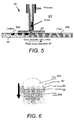
- An injector head 83 communicates with the reservoir 81 and is in contact with the mold plate 82.
- Mold plate 82 is scanned under the injector head 83 in the scan direction 87 and molten solder is injected through a solder slot 89 formed at the bottom of the injector head 83 and fills the empty cavities 85a in the mold 82.
- the filled mold plate is then cooled and inspected at the MIT 200.
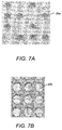
- FIG. 7A depicts a glass mold plate 82 with unfilled cavities 85a
- FIG. 7B depicts a glass mold with filled cavities 85b. Cavities 85 are etched on the glass mold 82 according to the required bump pattern.
- the glass mold 82 has a thermal expansion coefficient (CTE) similar to the CTE of the semiconductor wafer 72.
- CTE thermal expansion coefficient
- the solder transfer process 38 includes bringing together a wafer 74 patterned with under bump metallurgy (UBM) structures 73 with a mold plate 82 having solder filled cavities 85b (92). Next, heating the mold 82 and the wafer 74 to a temperature of 20 degrees higher than the solder melting point (94) and then bringing the mold 82 and wafer 74 in close proximity ( about 20 micrometers) or soft contact so that the solder wets the UBM structures 73 (96). The solder bumps from the cavities 85b are transferred to the UBM structures 73 and stay on the wafer 74 after the mold 82 separates from the wafer 74 (98).
- UBM under bump metallurgy
- a critical aspect of this process is the alignment of the mold plate 82 relative to the semiconductor wafer 74 so that the solder bumps 85b are transferred to precise UBM structures 73.
- the alignment needs to be maintained during the transport of the aligned mold-wafer system from station to station and during the actual solder transfer process at the required temperature, atmosphere and pressure.
- a fixture tool for holding and transferring the aligned mold and semiconductor structures together is described in a related co-pending application No.: 12/025644, entitled " Apparatus and Method for Semiconductor Bumping via Injection Molded Solder", the contents of which are incorporated herein by reference.
- the mold fill apparatus 700 includes a mold aligner 710, a mold pre-heat unit 720, a mold cool unit 730, and the mold fill tool(MFT) 100. Inserting a room temperature glass mold plate 82 in the high temperature MFT tool 100 causes the mold sides to bend upward (warping). Placing the room temperature mold 82 in the mold pre-heat unit 720 and preheating it to a temperature just below the solder melting point before inserting it in the MFT reduces the warping problem. Referring to FIG. 10 , and FIG.
- the mold pre-heat unit 720 includes a hot plate 728 heated with cartridge heaters, a robot end effector 116, a hot plate support plate 723, a mount and leveling assembly for the support plate 724, a gas supply line 727 and an exhaust 726.
- the mold is preheated to 200 C and the solder melting point is 217 C. Bringing the hot mold plate from the high temperature MFT tool 100 directly to room temperature also causes warping of the glass mold plate due to the uncontrolled and quick cool down process. To prevent warping during cool down, at the end of the mold filling process, the mold is placed onto the mold cool unit 730 where it is cooled down in a controlled way. Referring to FIG.
- the mold cool unit 730 includes a cool plate 736 which is cooled with an air chiller 732.
- the mold is supported on top of the plate 736 with three lift pins 734a-734c.
- Gas line 735 supplies the gas for the air chiller 732.
- Cool plate is mounted on top of a support plate 733 which is mounted on top of the leveling assembly 731.
- Cool plate 736 is made of a good thermal conductor material. In one example, it is made of aluminum.
- the MFT tool 100 includes a table 101 having a top 102 upon which a carriage assembly 140 and a solder head assembly 130 are mounted.
- a mold plate 82 with unfilled cavities is placed in the carriage assembly 140 and is scanned (i.e., moved) under the solder head assembly 130 along direction 602a, shown in FIG. 13 .
- Carriage assembly 140 includes a hot plate assembly 110, a start space 150 and a finish space 160, as shown in FIG. 14 .
- the hot plate assembly 110 includes a stage 112 that moves on rails 111a, 111b. Stage 112 supports the hot plate 114 upon which the mold 82 plate is mounted.
- a robot end effector (REF) 116 moves the mold plate 82 on and off the hot plate 114, shown in FIG. 15 .
- the positioning of the mold on and off the plate is guided with four mold guide pins 181a, 181b, 181c, 181d.
- the ends of each pin 181a-181d are frusto-conically shaped and are positioned and dimensioned so that their conical sides 182 guide the rounded edges 82a of the mold plate 82 and move the plate 82 sidewise, up or down as the pins move up or down, as shown in FIG. 17 and FIG. 18 , respectively.
- Table 101 also includes gas supply lines 103 and pressure control valves 104.
- hot plate 114 is mounted on top of a hot plate insulator 115 which in turn is mounted on top of a backing plate 115a.
- insulator plate 115 is made of Calcium Silicate.
- Cartridge heaters 117 are used for heating the hot plate 114.
- the top surface 118 of the hot plate 114 includes grooves 119 having small holes through which vacuum is drawn. The vacuum is used to hold the mold 82 onto the hot plate 114.
- Mold 82 is kinematically mounted on top of the hot plate 114 via a three pin motorized mount 170, shown in FIG. 23 .
- Pins 172a, 172b, 172c are arranged at 120 degree angles relative to each other and are used to guide the lifting and lowering of the mold 82 onto the hot plate 114.
- Mount 170 includes three arms 173a, 173b, 173c extending from the center 175 at 120 degrees angles relative to each other.
- Pins 172a, 172b, 172c extend upward from the top surfaces of the ends of each arm 173a, 173b, 173c, respectively.
- pins 172a-172c are made of polyamide.
- the start space assembly 150 includes a starting parking space 152 which is mounted on top of the base parking element 157.
- Starting parking space 152 includes a V-groove 152v on it bottom surface.
- Base parking element 157 is mounted on top of insulator plate 154 and insulator plate 154 is mounted on top of backing plate 154a.
- a ceramic spacer 153 separates the backing plate 154a from the first leveling plate 156 which is mounted on top of a second leveling plate 155.
- Leveling plate 155 is mounted on top of support plate 158, which in turn is set on top of the hot plate sled 111.
- finish space assembly 160 is on the opposite end of the carriage assembly 140.
- the finish space assembly 160 includes the finish V-groove parking space 162 which is mounted on top of the base parking element 167.
- Base parking element 167 is mounted on top of insulator plate 164 and insulator plate 164 is mounted on top of backing plate 164a.
- a ceramic spacer 163 separates the backing plate 164a from the first leveling plate 166 which is mounted on top of a second leveling plate 165.
- Leveling plate 165 is mounted on top of support plate 168, which in turn is set on top of the hot plate sled 111.
- finish space assembly 160 includes a fixed stop heat sink 161 adjacent to the finish parking space 162.
- An air cylinder 251 connects the fixed stop 161 with the base parking element 167.
- Both parking spaces 152, 162 are heated to a temperature slightly above the melting point of the solder used for filling the mold cavities with cartridge heaters 174.
- the solder head (or gantry) assembly 130 includes two support elements 131a, 131b, supporting an injector head slide assembly 133 carrying an injector head assembly 132, an injector head lift cylinder 134, two pairs of first and second parking space lifters 135a, 135b (not shown) and 135c, 135d, a parking space cleaner assembly 136 and two process gas heaters 137a, 137b.
- the parking space lifters 135a-135d are designed to pick up the start or finish parking spaces 152, 162 and lift them up or down in the direction of 138.
- the injector head slide assembly 133 includes a cross bar 133a having two downward extending legs 133b, 133c.
- the bottoms of legs 133b, 133c extend sidewise to provide mounting surfaces for the injector head assembly end plates 241a, 241b, shown in FIG. 26 .
- the mounting mechanism in areas A and B stabilizes the position of the reservoir 230 while allowing for small thermal expansions sidewise in the direction of 242.
- the injector head slide assembly is made of a material that has very low coefficient of thermal expansion (CTE) and remains stable at high temperatures.
- head slide assembly 130 is made of Invar alloy.
- the injector head assembly 132 includes a solder reservoir block 230 and hot gas skirt elements 231a, 231b having hot gas feeds 238a, 238b.
- Reservoir block 230 has a cap 239 and thermocouple feeds 236a, 236b leading two separate thermocouples 237a, 237b, to two different prearranged heights of the solder baths.
- a valid thermocouple reading indicates that the solder bath level is at the prearranged height where the thermocouple is mounted.
- the two thermocouple readings are used to monitor the fill level of the solder bath. More than two thermocouples may be used and a finer height selection may be arranged.
- the reservoir block 230 is supported with two hard end plates 241a, 241b at the bottom of the injector head slide assembly 133 in areas A and B, as shown in FIG. 26 .
- the bottom surface 230a of reservoir 230 includes a slot 234 surrounded by O-ring 233.
- surface 230a is brought into contact with the mold plate and molten solder is injected through slot 234 into the mold cavities.
- O-ring 233 is designed to sustain the high melt temperatures of solder.
- Hot gas is blown onto and around the bottom surface 230a through the hot gas skirt elements 231a, 231b.
- the hot gas is a mixture of nitrogen with air and the gas temperature is 200 C.
- the solder reservoir block is heated to a temperature above the solder melting point with cartridge heaters 243a, 243b.
- the hot plate carriage assembly 140 carrying the mold 82 on its top is scanned under the solder head assembly 130 in the direction of 602a for the mold filling process.
- the process of scanning the mold plate under the injector and the parking space mechanism is described with reference to FIG. 33-37 .
- the injector head 132 is positioned on the heated start parking space 152 and the mold 82 is loaded onto the hot plate 114 which is placed in the center of the carriage assembly 140 (step 1), as shown in FIG. 38 .
- Edge 152a of the start parking space is shown in FIG. 33 to have some solder deposit from the previous run.
- the support pins 172a-172c are lowered and the mold 82 is brought in contact with the hot plate 114 (step 2).
- the finish parking space 162 is then moved to the fixed stop 161b at low pressure (step 3) and then the edge 82a of the mold 82 is aligned with the finish parking space edge 162a, as shown in FIG. 37 (step 4).
- the start parking space 152 is also moved to the X-axis encoder position 161a.
- the positions of the start parking space 152 and the finish parking space 162 are locked and the vacuum for holding the mold 82 onto the hot plate 114 is turned on to secure the aligned mold onto the hot plate 114 during scanning.
- the hot plate assembly 140 is scanned in the direction 602a so that the mold plate 82 is positioned under the stationary injector head 132, as shown in step 5 of FIG. 33 and FIG. 38 .
- the transition of the injector head 132 from the start parking space 152 onto the mold plate 82 causes solder residue to be deposited onto edge 152b of the parking space 152, shown in FIG. 33 .
- the solder deposits from edges 152a, 152b of the start parking space 152 are cleaned at the cleaner assembly 136 (step 6) and then the clean start parking space 152 is picked up by the second lifter 135b, as shown in step 7 of FIG. 34 and FIG. 38 .
- the mold 82 is scanned under the injector head 132 for filling of the mold cavities with solder while the start parking space 152 is carried by the second lifter 135b, as shown in FIG. 38 (step 8).
- the head 132 When all cavities are filled the head 132 is at a position to be deposited onto the finish parking space 162, as shown in step 9 in FIG. 39 . At this transition point, edge 162a of the finish parking base 162 is contaminated with solder deposit from the injector head 132.
- the head 132 is positioned onto the finish parking space 162 (step 9) and the mold/ hot plate assembly separate from the finish parking space 162 (step 10).
- the head 132 lifts up the finish parking space 162 (step 11) and the second lifter 135b places the clean start parking space 152 onto the finish base 167, as shown in FIG. 39 and FIG. 35 (step 12).
- the filled mold 82 is scanned under the injector head 132 carrying the finish parking space 162 in the opposite direction 602b (step 13) until it reaches the position where the injector head is above the start base 157 (step 14). At this point the injector head 132 deposits the finish parking base 162 onto the start base 157 (step 15), shown in FIG. 35 .
- the filled mold is unloaded and an empty mold is loaded onto the hot plate and the process repeats again. Excess solder escaping from the injector head when the head is transferred from the mold onto and off the parking spaces is captured at the sides of hot plate 114 in the solder catchers 199, shown in FIG. 16 .
- the HVM MFT is designed to fill the mold cavities when the mold 82 is scanned in the direction of 602a and to return the filled mold back in the starting position before repeating the filling process with a new mold.
- This one-way deposition ensures that edge 233a of the injector head O-ring 233 is always in contact with the molten solder 246 that is injected through the slot 234 and edge 233b is always in contact with the hot air mixture of air (or oxygen) and nitrogen 246.
- An oxide layer 248 is formed at the bottom surface of the O-ring and is always in contact with the mold surface, as shown in FIG. 32 .
- This particular scanning limitation is important for the repeatability of the deposition parameters and reduction of defects.
- both parking spaces 152, 162 are heated to a temperature slightly above the melting point of the solder used for filling the mold cavities and the mold 82 floats above the hot plate 114 during the scanning process and is held in place by vacuum.
- Glass mold 82 is square shaped and the left edge of the square is aligned against the end parking space to correct for any dimensional imperfections of the mold that may lead to solder bump defect formation.
- mold 82 is a square having a side of 14 inches long. There is a border around the square mold surface that does not carry any patterned cavities. The edges of the start and finish parking spaces 152, 162 that were contaminated with solder deposit during the mold fill process are cleaned at the cleaner assembly 136, shown in FIG. 40 .
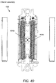
- Cleaner assembly 136 includes two rotating brushes 604a, 604b.
- An alternative injector head design that does not cause contamination of the parking space edges and mold edges is shown in FIG. 42 .
- the injector head 605 includes capillaries 608 through which air is blown to "freeze off" the molten solder before lifting the injector head from the mold or parking space surfaces.
- Chatter is caused by small vibrations of the injector head and can lead to skipping along the glass mold and either not filling a cavity or partially filling a cavity.
- One way of reducing chatter is to hold down the injector head onto the glass mold by clamping the solder head assembly onto the glass mold and applying pressure.
- Tipping refers to small forward or backward tilting of the injector head and can also lead to partially filled cavities, non-uniform sized bumps and bridges. The above mentioned clamping and applying pressure solution addresses this problem, as well.
- Head warping is caused by thermal gradients along the length of the injector head and can cause the injector head side ends to bend up or down.
- One way of reducing head warping is by heating the injector cap separately and by adding separate heaters along the length of the injector heads. In one example, the head is furnished with evenly spaced holes carrying low wattage cartridge heaters and the head is slightly compressed onto the mold.
- the unfilled mold plates are cleaned at the air knife table 650, shown in FIG. 41 .
- a combination of ultrasonic vibrations and blowing of ionized air is used to release and remove contaminants from the mold surface.
- the contaminates are removed by drawing a vacuum on the mold surface.
Landscapes
- Engineering & Computer Science (AREA)
- Mechanical Engineering (AREA)
- Moulds For Moulding Plastics Or The Like (AREA)
Description
- The present invention relates to an apparatus for filling patterned mold cavitus formed on a surface of a mold structure with solder according to the preamble of
claim 1, for semiconductor wafer bumping, and more particularly to semiconductor wafer bumping via an injection molded solder process. - Injection Molded Solder (IMS) is a process used to produce solder bumps on a semiconductor wafer surface. Referring to
FIG. 1 , theIMS process 30 includes depositing solder into mold cavities (34), forming a pattern on the semiconductor wafer surface (32), aligning the filled mold cavities with the patterned semiconductor wafer surface and then transferring the solder from the mold cavities to the semiconductor wafer surface (38). Solder bumps are formed in aglass mold plate 82 by injecting molten solder into the etched mold cavities. The etched cavities match the pattern of solder bumps required on the semiconductor wafer surface. The process provides fine pitch placement of the solder bumps in the range of 10 to 500 micrometers separation distance between adjacent solder bumps. - The IMS process has been tested and applied for laboratory scale applications. It is desirable to provide a scale-up process and a high volume manufacturing (HVM) apparatus designed to optimize the high volume manufacturing process. A critical aspect of the scale-up process involves the complete filling of the mold cavities. It is desirable to fill all mold cavities uniformly with solder without leaving some cavities either not filled or partially filled or overfilled.
-
US 6 231 333 B1 , representing the prior art, discloses an apparatus for filling patterned mold cavities on a surface of a mold structure with solder. -
US 6 182 356 B1 discloses an apparatus for loading solder balls into a mold. -
US 2006/289607 A1 discloses a composite solder transfer moldplate structure. - The invention provides an apparatus for filling patterned mold cavities form on a surface of a mold structure with solder, as defined in
claim 1. In general, in one aspect, the invention features an apparatus for filling patterned mold cavities formed on a surface of a mold structure with solder. The apparatus includes an injector head assembly comprising a solder reservoir having a bottom surface with an elongated slot for injecting solder into the mold cavities and a carriage assembly configured to carry and scan the mold structure under the injector head assembly. The mold structure is brought into contact with the solder reservoir bottom surface and a seal is formed between an area of the solder reservoir bottom surface surrounding the elongated slot and the mold structure surface and then the mold cavities are filled with solder by scanning the mold structure under the injector head in a first direction from a starting position to a finish position while solder is injected into them and then the mold structure with the filled mold cavities is returned back to the starting position by scanning it in a second direction opposite to the first direction without any further solder injection. The carriage assembly includes first and second parallel rails, a plate assembly movable upon the first and second parallel rails, a start parking space and a finish parking space. The mold structure is placed upon the movable plate assembly for performing the scanning under the injector head assembly. Each of the parking spaces includes a parking plate having a V-groove on its bottom surface, a heated base supporting the parking plate, an insulator plate supporting the heated base, a back plate supporting the insulator plate and first and second leveling plates configured to level the back plate. - Implementations of this aspect of the invention may include one or more of the following features. The solder reservoir is heated to a temperature above the solder melting point and is slightly pressurized. The apparatus further includes a preheat station where the mold structure is preheated to a temperature slightly below the solder melting temperature prior to the scanning and filling of the mold cavities with solder. The apparatus further includes a cool down station where the mold structure is slowly cooled down to room temperature after the filling of the mold cavities with solder. The apparatus further includes an aligner for aligning the mold structure prior to the scanning and filling of the mold cavities with solder. The injector head assembly remains stationary during the scanning in the first and second directions of the mold structure. The plate assembly includes a heated plate upon which mold structure is mounted, a non-heated back plate and an insulator plate placed between the heated plate and the back plate. The mold structure is kinematically mounted onto the heated plate via three motorized pins and wherein the three motorized pins are arranged at 120 degree angle relative to each other and are used for lowering and raising the mold structure onto the heated plate. The heated base and the heated plate upon which the mold structure is mounted are heated to a temperature slightly above the solder melting point. The injector head assembly further includes a hot gas skirt surrounding the solder reservoir bottom surface and being configured to blow hot gas onto it. The injector head assembly further comprises an O-ring surrounding the elongated slot and forming the seal between an area of the solder reservoir bottom surface surrounding the elongated slot and the mold structure surface. The O-ring is made of a material capable of withstanding the solder melt temperature. The apparatus further includes an injector head slide assembly and the injector head assembly is supported and mounted onto the injector head slide assembly via a mounting mechanism that stabilizes the injector head assembly position while allowing for small thermal sidewise expansions, along the direction of the elongated slot. The apparatus further includes a support frame supporting the injector head slide assembly and first and second parking space lifters. The first and second parking space lifters are configured to pick the start and finish parking plates, respectively and raise them up or lower them down onto the corresponding heated bases. The apparatus further includes a parking plate cleaner configured to clean the parking plates. The injector head slide assembly is made of a material with low coefficient of thermal expansion. The apparatus further includes one or more thermocouples inserted into the solder reservoir at various heights and the thermocouples produce thermocouple readings used to measure solder fill levels in the solder reservoir. The injector head assembly may further include capillaries through which air is blown toward the elongated slot for freezing any molten solder.
- With the apparatus according to the invention, a method for filling patterned mold cavities formed on a first surface of a mold structure with solder can be performed, including the following steps. First providing an injector head assembly comprising a solder filled reservoir having a bottom surface with an elongated slot for injecting solder through the elongated slot into the mold cavities. Next, providing a carriage assembly configured to carry and scan the mold structure under the injector head assembly and loading the mold structure onto the carriage assembly. Next, bringing the mold structure in contact with the solder reservoir bottom surface and the elongated slot and forming a seal between an area of the solder reservoir bottom surface surrounding the elongated slot and the mold structure surface and then scanning the mold structure under the injector head assembly in a first direction from a starting position to a finish position while injecting molten solder into the mold cavities and then scanning the filled mold structure in a second direction opposite to the first direction, without any further solder injection, for returning the mold structure back from the finish position to the starting position. The scanning step includes the following. First, positioning the injector head assembly upon the heated start parking space and then loading and centering the mold structure onto the plate assembly, so that is in contact with a heated plate. Next, moving the heated finish parking space to a fixed stop and aligning an edge of the finish parking space with an adjacent edge of the mold structure. Next, moving the start parking space with the injector head assembly to a start position and then locking the start and finish parking space positions. Next, scanning the heated plate with the mold structure in the first direction so that the injector head assembly is moved from the start parking space onto the mold structure. Next, cleaning any solder deposits from the start parking plate and lifting the start parking plate from the start parking space with the first parking space lifter. Next, continue scanning the heated plate with the mold structure under the injector head assembly and the lifted start parking plate in the first direction while injecting solder into the mold cavities until all mold cavities are filled with solder. Next, positioning the injector head assembly onto the finish parking space and placing it in contact with the finish parking plate. Next, separating the heated plate with the filled mold structure from the finish parking space. Next, lifting the injector head assembly with the finish parking plate from the finish parking space and placing the cleaned start parking plate onto the finish parking space. Next, scanning the heated plate with the filled mold structure in the second direction under the finish parking plate and injector head assembly until reaching the start parking space. Finally, placing the finish parking plate with the injector head assembly onto the start parking space and unloading the filled mold structure.
- The method may further include positioning and aligning a patterned first surface of a semiconductor structure directly opposite to the solder filled patterned mold cavities of the mold structure. Next, providing a fixture tool for holding and transferring the aligned mold and semiconductor structures together. Next, receiving the fixture tool with the aligned mold and semiconductor structures and transferring the solder from the aligned patterned mold cavities to the aligned patterned semiconductor first surface. The mold cavities pattern matches the semiconductor surface pattern.
- Referring to the figures, wherein like numerals represent like parts throughout the several views:
-
FIG. 1 is a schematic diagram of a laboratory scale Injection Molded Solder (IMS) process; -
FIG. 2 is a schematic diagram of a scale-up IMS process according to this invention; -
FIG. 3 is a block diagram of the scale-up IMS process flow; -
FIG. 4 is a schematic diagram of the HVM IMS equipment system according to this invention; -
FIG. 5 is a schematic diagram of the mold fill process; -
FIG. 6 is a diagram of a partially filled mold plate; -
FIG. 7A depicts a mold with unfilled cavities; -
FIG. 7B depicts a mold with filled cavities; -
FIG. 8 is a schematic diagram of the solder transfer process; -
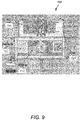
FIG. 9 depicts the HVM MFT equipment system of this invention; -
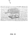
FIG. 10 depicts the mold preheat station; -
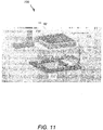
FIG. 11 depicts the mold preheat station ofFIG. 10 without a cover; -
FIG. 12 depicts the mold cooling station; -
FIG. 13 depicts the HVM MFT station; -
FIG. 14 depicts the hot plate assembly components of the HVM MFT station ofFIG. 13 ; -
FIG. 15 depicts the hot plate assembly with a mold; -
FIG. 16 is a detailed side view of the hot plate assembly ofFIG. 15 ; -
FIG. 17 is a detailed side view of the mold pin alignment mechanism with the pin up; -
FIG. 18 is a detailed side view of the mold pin alignment mechanism with the pin down; -
FIG. 19 is a perspective view of the staring parking space; -
FIG. 20 is a side view of the staring parking space; -
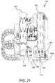
FIG. 21 is a perspective view of the finish parking space; -
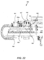
FIG. 22 is a side view of the finish parking space; -
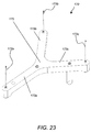
FIG. 23 is a side perspective view of the three pin motorized mount system; -
FIG. 24 is a front perspective view of the solder head assembly; -
FIG. 25 is a front perspective view of the injector head; -
FIG. 26 is a front view of the injector head; -
FIG. 27 is a top view of the injector head; -
FIG. 28 is a perspective view of the injector reservoir; -
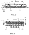
FIG. 29 is a front view of the injector reservoir ofFIG. 28 ; -
FIG. 30 is a bottom view of the injector reservoir ofFIG. 28 ; -
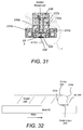
FIG. 31 is a detailed view of section A-A of the injector reservoir ofFIG. 29 ; -
FIG. 32 is a cross-sectional view of the O-ring ofFIG. 30 ; -
FIG. 33 - FIG. 36 are schematic diagrams of the process steps of scanning the hot plate under the injector head; -
FIG. 37 illustrates the mold alignment process against the finish parking space; -
FIG. 38-FIG. 39 illustrate the process steps of scanning the hot plate under the injector head and the function of the start and finish parking spaces; -
FIG. 40 depicts a bottom view of the cleaner assembly for the parking spaces; -
FIG. 41 depicts the air knife slide table; and -
FIG. 42 is another embodiment for the injector head. - Referring to
FIG. 2 , the scale-up IMS process 50 includes filling mold cavities with solder (34), inspecting the filled mold plate (86), forming a pattern on the semiconductor wafer surface (32), inspecting the wafer surface (75) and then transferring the solder from the mold cavities to the semiconductor wafer surface (38). Referring toFIG. 3 , the scale-up IMS process 50 further includes cleaning of the molds at a moldclean station 60, filling of the mold cavities with solder and inspecting the filled mold plate at amold prepare station 80, and transferring of the solder from the mold cavities onto the patterned semiconductor wafer surface at awafer bump station 90. The mold preparestation 80 includes a mold fill tool (MFT) 100, a mold inspect tool (MIT) 200, and amold repair tool 88. Thewafer bump station 90 includes a solder transfer tool (STT) 300 and awafer loader tool 400.New molds 61 and previously usedmolds 62 pass through the moldclean station 60 where they get cleaned with anacid solution 63 and abase solution 64. Theclean molds 82 enter amold stocker 500 and from there they are introduced into theMFT 100. After filling the mold cavities with solder, the molds are inspected at theMIT 200 and then transferred to aready mold stocker 550. Molds that do not pass inspection are either recycled at the moldclean station 60 or are repaired at therepair tool 88. Molds that are repaired pass through theMIT 200 again and upon passing the inspection are transferred toready mold stocker 550. In some embodiments themold repair tool 88 is integrated with theMIT 200. From theready mold stocker 550 the molds are introduced into theSTT 300. Patternedwafers 74 are introduced into thewafer loader 400 and from there into theSTT 300. After the solder transfer process the bumpedwafers 76 exit thewafer bump station 90 and the dirty molds 62b are introduced into the moldclean station 60 again. The process repeats until allwafers 74 are bumped. A schematic diagram of the HVMIMS equipment system 52 is shown inFIG. 4 . It includes the moldclean station 60, themold stocker 500, theMFT 100, theMIT 200, theSTT 300, the wafer loader, i.e., front open unified pod (FOUP) 400 and amold cart 600. In one example, theHVM system 52 has a capacity of 300 wafer per day (1 wafer every 4 minutes) and 350 molds per day (1 mold every 3.5 minutes). It provides automation of the wafer and mold transfer. The STT can process 200 mm and 300 mm wafers without any hardware changes and each mold carrier can carry up to 25 molds. The molds are identified with a bar code mechanism and the mold stocker/sorter is integrated in the process line. There is also an integrated mold and wafer tracking and management system. The system can accommodate any solder type including no lead/eutectic PbSn (low temperature) at start up and high lead later. - Referring to
FIG. 5 and FIG 6 , themold fill process 34 includes melting bulk solder (wire, shots, slugs) in areservoir 81.Reservoir 81 is heated above the melting point of the solder and is slightly pressurized. Aninjector head 83 communicates with thereservoir 81 and is in contact with themold plate 82.Mold plate 82 is scanned under theinjector head 83 in the scan direction 87 and molten solder is injected through asolder slot 89 formed at the bottom of theinjector head 83 and fills theempty cavities 85a in themold 82. The filled mold plate is then cooled and inspected at theMIT 200.FIG. 7A depicts aglass mold plate 82 withunfilled cavities 85a andFIG. 7B depicts a glass mold with filledcavities 85b. Cavities 85 are etched on theglass mold 82 according to the required bump pattern. Theglass mold 82 has a thermal expansion coefficient (CTE) similar to the CTE of thesemiconductor wafer 72. - Referring to
FIG. 8 , thesolder transfer process 38 includes bringing together awafer 74 patterned with under bump metallurgy (UBM) structures 73 with amold plate 82 having solder filledcavities 85b (92). Next, heating themold 82 and thewafer 74 to a temperature of 20 degrees higher than the solder melting point (94) and then bringing themold 82 andwafer 74 in close proximity ( about 20 micrometers) or soft contact so that the solder wets the UBM structures 73 (96). The solder bumps from thecavities 85b are transferred to the UBM structures 73 and stay on thewafer 74 after themold 82 separates from the wafer 74 (98). A critical aspect of this process is the alignment of themold plate 82 relative to thesemiconductor wafer 74 so that the solder bumps 85b are transferred to precise UBM structures 73. The alignment needs to be maintained during the transport of the aligned mold-wafer system from station to station and during the actual solder transfer process at the required temperature, atmosphere and pressure. A fixture tool for holding and transferring the aligned mold and semiconductor structures together is described in a related co-pending application No.: 12/025644, entitled " Apparatus and Method for Semiconductor Bumping via Injection Molded Solder", the contents of which are incorporated herein by reference. - Referring to
FIG. 9 , themold fill apparatus 700 includes amold aligner 710, a moldpre-heat unit 720, a moldcool unit 730, and the mold fill tool(MFT) 100. Inserting a room temperatureglass mold plate 82 in the hightemperature MFT tool 100 causes the mold sides to bend upward (warping). Placing theroom temperature mold 82 in the moldpre-heat unit 720 and preheating it to a temperature just below the solder melting point before inserting it in the MFT reduces the warping problem. Referring toFIG. 10 , andFIG. 11 the moldpre-heat unit 720 includes ahot plate 728 heated with cartridge heaters, arobot end effector 116, a hotplate support plate 723, a mount and leveling assembly for thesupport plate 724, agas supply line 727 and anexhaust 726. In one example, the mold is preheated to 200 C and the solder melting point is 217 C. Bringing the hot mold plate from the hightemperature MFT tool 100 directly to room temperature also causes warping of the glass mold plate due to the uncontrolled and quick cool down process. To prevent warping during cool down, at the end of the mold filling process, the mold is placed onto the moldcool unit 730 where it is cooled down in a controlled way. Referring toFIG. 12 the moldcool unit 730 includes acool plate 736 which is cooled with anair chiller 732. The mold is supported on top of theplate 736 with three lift pins 734a-734c.Gas line 735 supplies the gas for theair chiller 732. Cool plate is mounted on top of asupport plate 733 which is mounted on top of the levelingassembly 731.Cool plate 736 is made of a good thermal conductor material. In one example, it is made of aluminum. - Referring to
FIG. 13 theMFT tool 100 includes a table 101 having a top 102 upon which acarriage assembly 140 and asolder head assembly 130 are mounted. Amold plate 82 with unfilled cavities is placed in thecarriage assembly 140 and is scanned (i.e., moved) under thesolder head assembly 130 alongdirection 602a, shown inFIG. 13 . During this scanning molten solder is injected from the stationary solder head assembly into the mold cavities.Carriage assembly 140 includes ahot plate assembly 110, astart space 150 and afinish space 160, as shown inFIG. 14 . Thehot plate assembly 110 includes astage 112 that moves onrails Stage 112 supports thehot plate 114 upon which themold 82 plate is mounted. A robot end effector (REF) 116 moves themold plate 82 on and off thehot plate 114, shown inFIG. 15 . The positioning of the mold on and off the plate is guided with fourmold guide pins pin 181a-181d are frusto-conically shaped and are positioned and dimensioned so that theirconical sides 182 guide therounded edges 82a of themold plate 82 and move theplate 82 sidewise, up or down as the pins move up or down, as shown inFIG. 17 andFIG. 18 , respectively. Table 101 also includesgas supply lines 103 andpressure control valves 104. - Referring to
FIG. 16 ,hot plate 114 is mounted on top of ahot plate insulator 115 which in turn is mounted on top of abacking plate 115a. In oneexample insulator plate 115 is made of Calcium Silicate.Cartridge heaters 117 are used for heating thehot plate 114. The top surface 118 of thehot plate 114 includesgrooves 119 having small holes through which vacuum is drawn. The vacuum is used to hold themold 82 onto thehot plate 114.Mold 82 is kinematically mounted on top of thehot plate 114 via a three pinmotorized mount 170, shown inFIG. 23 .Pins mold 82 onto thehot plate 114.Mount 170 includes threearms center 175 at 120 degrees angles relative to each other.Pins arm example pins 172a-172c are made of polyamide. - Referring to
FIG. 19 andFIG. 20 thestart space assembly 150 includes a startingparking space 152 which is mounted on top of thebase parking element 157. Startingparking space 152 includes a V-groove 152v on it bottom surface.Base parking element 157 is mounted on top ofinsulator plate 154 andinsulator plate 154 is mounted on top ofbacking plate 154a. Aceramic spacer 153 separates thebacking plate 154a from thefirst leveling plate 156 which is mounted on top of asecond leveling plate 155. Levelingplate 155 is mounted on top ofsupport plate 158, which in turn is set on top of thehot plate sled 111. - A mirror image finish
parking space assembly 160 is on the opposite end of thecarriage assembly 140. Referring toFIG. 21 andFIG. 22 thefinish space assembly 160 includes the finish V-groove parking space 162 which is mounted on top of thebase parking element 167.Base parking element 167 is mounted on top ofinsulator plate 164 andinsulator plate 164 is mounted on top ofbacking plate 164a. Aceramic spacer 163 separates thebacking plate 164a from thefirst leveling plate 166 which is mounted on top of asecond leveling plate 165. Levelingplate 165 is mounted on top ofsupport plate 168, which in turn is set on top of thehot plate sled 111. In addition to these elements, finishspace assembly 160 includes a fixedstop heat sink 161 adjacent to thefinish parking space 162. An air cylinder 251 connects the fixedstop 161 with thebase parking element 167. Bothparking spaces cartridge heaters 174. - Referring to
FIG. 24 , the solder head (or gantry)assembly 130 includes twosupport elements head slide assembly 133 carrying aninjector head assembly 132, an injectorhead lift cylinder 134, two pairs of first and secondparking space lifters cleaner assembly 136 and twoprocess gas heaters parking space lifters 135a-135d are designed to pick up the start or finishparking spaces - Referring to
FIG. 25- FIG. 26 the injectorhead slide assembly 133 includes across bar 133a having two downward extendinglegs legs assembly end plates FIG. 26 . The mounting mechanism in areas A and B stabilizes the position of thereservoir 230 while allowing for small thermal expansions sidewise in the direction of 242. The injector head slide assembly is made of a material that has very low coefficient of thermal expansion (CTE) and remains stable at high temperatures. In one example,head slide assembly 130 is made of Invar alloy. - Referring to
FIG. 27-FIG. 30 , theinjector head assembly 132 includes asolder reservoir block 230 and hotgas skirt elements hot gas feeds Reservoir block 230 has acap 239 andthermocouple feeds separate thermocouples 237a, 237b, to two different prearranged heights of the solder baths. A valid thermocouple reading indicates that the solder bath level is at the prearranged height where the thermocouple is mounted. The two thermocouple readings are used to monitor the fill level of the solder bath. More than two thermocouples may be used and a finer height selection may be arranged. Thereservoir block 230 is supported with twohard end plates head slide assembly 133 in areas A and B, as shown inFIG. 26 . - Referring to
FIG. 30 thebottom surface 230a ofreservoir 230 includes aslot 234 surrounded by O-ring 233. For the mold filling process,surface 230a is brought into contact with the mold plate and molten solder is injected throughslot 234 into the mold cavities. O-ring 233 is designed to sustain the high melt temperatures of solder. Hot gas is blown onto and around thebottom surface 230a through the hotgas skirt elements cartridge heaters - As was mentioned above, the hot
plate carriage assembly 140 carrying themold 82 on its top is scanned under thesolder head assembly 130 in the direction of 602a for the mold filling process. The process of scanning the mold plate under the injector and the parking space mechanism is described with reference toFIG. 33-37 . Initially theinjector head 132 is positioned on the heatedstart parking space 152 and themold 82 is loaded onto thehot plate 114 which is placed in the center of the carriage assembly 140 (step 1), as shown inFIG. 38 .Edge 152a of the start parking space is shown inFIG. 33 to have some solder deposit from the previous run. Next, the support pins 172a-172c are lowered and themold 82 is brought in contact with the hot plate 114 (step 2). Thefinish parking space 162 is then moved to the fixedstop 161b at low pressure (step 3) and then theedge 82a of themold 82 is aligned with the finishparking space edge 162a, as shown inFIG. 37 (step 4). Thestart parking space 152 is also moved to theX-axis encoder position 161a. Next, the positions of thestart parking space 152 and thefinish parking space 162 are locked and the vacuum for holding themold 82 onto thehot plate 114 is turned on to secure the aligned mold onto thehot plate 114 during scanning. Thehot plate assembly 140 is scanned in thedirection 602a so that themold plate 82 is positioned under thestationary injector head 132, as shown instep 5 ofFIG. 33 andFIG. 38 . The transition of theinjector head 132 from thestart parking space 152 onto themold plate 82 causes solder residue to be deposited ontoedge 152b of theparking space 152, shown inFIG. 33 . Next, the solder deposits fromedges start parking space 152 are cleaned at the cleaner assembly 136 (step 6) and then the cleanstart parking space 152 is picked up by thesecond lifter 135b, as shown in step 7 ofFIG. 34 andFIG. 38 . Themold 82 is scanned under theinjector head 132 for filling of the mold cavities with solder while thestart parking space 152 is carried by thesecond lifter 135b, as shown inFIG. 38 (step 8). When all cavities are filled thehead 132 is at a position to be deposited onto thefinish parking space 162, as shown instep 9 inFIG. 39 . At this transition point,edge 162a of thefinish parking base 162 is contaminated with solder deposit from theinjector head 132. Thehead 132 is positioned onto the finish parking space 162 (step 9) and the mold/ hot plate assembly separate from the finish parking space 162 (step 10). Next, thehead 132 lifts up the finish parking space 162 (step 11) and thesecond lifter 135b places the cleanstart parking space 152 onto thefinish base 167, as shown inFIG. 39 andFIG. 35 (step 12). Then the filledmold 82 is scanned under theinjector head 132 carrying thefinish parking space 162 in theopposite direction 602b (step 13) until it reaches the position where the injector head is above the start base 157 (step 14). At this point theinjector head 132 deposits thefinish parking base 162 onto the start base 157 (step 15), shown inFIG. 35 . The filled mold is unloaded and an empty mold is loaded onto the hot plate and the process repeats again. Excess solder escaping from the injector head when the head is transferred from the mold onto and off the parking spaces is captured at the sides ofhot plate 114 in thesolder catchers 199, shown inFIG. 16 . - Referring to
FIG 32 , the HVM MFT is designed to fill the mold cavities when themold 82 is scanned in the direction of 602a and to return the filled mold back in the starting position before repeating the filling process with a new mold. This one-way deposition ensures thatedge 233a of the injector head O-ring 233 is always in contact with themolten solder 246 that is injected through theslot 234 andedge 233b is always in contact with the hot air mixture of air (or oxygen) andnitrogen 246. Anoxide layer 248 is formed at the bottom surface of the O-ring and is always in contact with the mold surface, as shown inFIG. 32 . This particular scanning limitation is important for the repeatability of the deposition parameters and reduction of defects. - As was mentioned above, both
parking spaces mold 82 floats above thehot plate 114 during the scanning process and is held in place by vacuum.Glass mold 82 is square shaped and the left edge of the square is aligned against the end parking space to correct for any dimensional imperfections of the mold that may lead to solder bump defect formation. In oneexample mold 82 is a square having a side of 14 inches long. There is a border around the square mold surface that does not carry any patterned cavities. The edges of the start and finishparking spaces cleaner assembly 136, shown inFIG. 40 .Cleaner assembly 136 includes tworotating brushes FIG. 42 . Theinjector head 605 includes capillaries 608 through which air is blown to "freeze off" the molten solder before lifting the injector head from the mold or parking space surfaces. - Problems with the injector head during the mold fill process include chatter, tipping and warping. Chatter is caused by small vibrations of the injector head and can lead to skipping along the glass mold and either not filling a cavity or partially filling a cavity. One way of reducing chatter is to hold down the injector head onto the glass mold by clamping the solder head assembly onto the glass mold and applying pressure. Tipping refers to small forward or backward tilting of the injector head and can also lead to partially filled cavities, non-uniform sized bumps and bridges. The above mentioned clamping and applying pressure solution addresses this problem, as well. Head warping is caused by thermal gradients along the length of the injector head and can cause the injector head side ends to bend up or down. One way of reducing head warping is by heating the injector cap separately and by adding separate heaters along the length of the injector heads. In one example, the head is furnished with evenly spaced holes carrying low wattage cartridge heaters and the head is slightly compressed onto the mold.
- Before the mold fill process the unfilled mold plates are cleaned at the air knife table 650, shown in
FIG. 41 . A combination of ultrasonic vibrations and blowing of ionized air is used to release and remove contaminants from the mold surface. The contaminates are removed by drawing a vacuum on the mold surface. - Several embodiments of the present invention have been described. Nevertheless, it will be understood that various modifications may be made without departing from the scope of the invention. Accordingly, other embodiments are within the scope of the following claims.
Claims (17)
- An apparatus for filling patterned mold cavities formed on a surface of a mold structure with solder comprising:an injector head assembly (132) comprising a solder reservoir (230) having a bottom surface (230a) with an elongated slot (234) for injecting solder into said mold cavities;a carriage assembly (140) configured to carry and scan said mold structure under said injector head assembly (132), characterized in that said carriage assembly (140) comprises first and second parallel rails, a plate assembly (110) movable upon said first and second parallel rails, a start parking space (152) and a finish parking space (162) and in that said mold structure is placed upon said movable plate assembly for performing said scanning under said injector head assembly (132) and in that each of said parking spaces (152, 162) comprises a parking plate having a V-groove (155v, 162v) on its bottom surface, a heated base supporting said parking plate, an insulator plate (154, 164) supporting said heated base, a back plate supporting said insulator plate and first and second leveling plates (156, 166) configured to level said back plate; andwherein, in use, said mold structure is brought into contact with said solder reservoir bottom surface (230a) and a seal is formed between an area of said solder reservoir bottom surface (230a) surrounding said elongated slot (234) and said mold structure surface and then said mold cavities are filled with solder by scanning said mold structure under said injector head (132) in a first direction from a starting position to a finish position while solder is injected into them and then said mold structure with the filled mold cavities is returned back to said starting position by scanning it in a second direction opposite to said first direction without any further solder injection.
- The apparatus of claim 1 wherein said solder reservoir (230) is heated to a temperature above said solder melting point and is slightly pressurized.
- The apparatus of claim 2 further comprising a preheat station (720) where said mold structure is preheated to a temperature slightly below said solder melting temperature prior to said scanning and filling of said mold cavities with solder.
- The apparatus of claim 3 further comprising a cool down station (730) where said mold structure is slowly cooled down to room temperature after said filling of said mold cavities with solder.
- The apparatus of claim 2 further comprising an aligner (710) for aligning said mold structure prior to said scanning and filling of said mold cavities with solder.
- The apparatus of claim 2 wherein said injector head assembly (132) remains stationary during said scanning in said first and second directions of said mold structure.
- The apparatus of claim 1 wherein said plate assembly (110) comprises a heated plate (114) upon which mold structure is mounted, a non-heated back plate (115a) and an insulator plate (115) placed between said heated plate (114) and said back plate (115a).
- The apparatus of claim 7 wherein said mold structure is kinematically mounted onto said heated plate (114) via three motorized pins (172a, 172b, 172c) and wherein said three motorized pins (172a, 172b, 172c) are arranged at 120 degree angle relative to each other and are used for lowering and raising said mold structure onto said heated plate (114).
- The apparatus of claim 1 wherein said heated base and said heated plate (114) upon which said mold structure is mounted are heated to a temperature slightly above said solder melting point.
- The apparatus of claim 9 wherein said injector head assembly (132) further comprises a hot gas skirt (231a-b) surrounding said solder reservoir (230) bottom surface (230a) and being configured to blow hot gas onto it.
- The apparatus of claim 10 wherein said injector head assembly (132) further comprises an O-ring (233) surrounding said elongated slot (234) and forming said seal between an area of said solder reservoir bottom surface (230a) surrounding said elongated slot (234) and said mold structure surface and wherein said O-ring (233) comprises a material capable of withstanding said solder melt temperature.
- The apparatus of claim 11 further comprising an injector head slide assembly (133) and wherein said injector head assembly (132) is supported and mounted onto said injector head slide assembly (133) via a mounting mechanism that stabilizes said injector head assembly (132) position while allowing for small thermal sidewise expansions, along the direction of the elongated slot (234), and wherein said injector head slide assembly (132) comprises a material with low coefficient of thermal expansion.
- The apparatus of claim 12 further comprising a support frame supporting said injector head slide assembly (133) and first and second parking space lifters (135a-d) wherein said first and second parking space lifters (135a-d) are configured to pick said start and finish parking plates respectively and raise them up or lower them down onto said corresponding heated bases.
- The apparatus of claim 13 further comprising a parking plate cleaner (136) configured to clean said parking plates.
- The apparatus of claim 12, 13 or 14 further comprising one or more thermocouples (237a, 237b) inserted into said solder reservoir (230) at various heights and wherein said thermocouples (237a, 237b) produce thermocouple readings used to measure solder fill levels in said solder reservoir (230).
- The apparatus of claim 1, comprising
equipment for positioning and aligning a patterned first surface of a semiconductor structure directly opposite to said solder filled patterned mold cavities of the mold structure;
a fixture tool for holding and transferring said aligned mold and semiconductor structures together; and
equipment for receiving said fixture tool with the aligned mold and semiconductor structures and transferring the solder from said aligned patterned mold cavities to said aligned patterned semiconductor first surface. - The apparatus of claim 11 wherein said injector head assembly (132) further comprises capillaries through which air is blown toward said elongated slot (234) for freezing any molten solder.
Applications Claiming Priority (3)
| Application Number | Priority Date | Filing Date | Title |
|---|---|---|---|
| US90873707P | 2007-03-29 | 2007-03-29 | |
| US12/056,369 US7703658B2 (en) | 2007-03-29 | 2008-03-27 | Apparatus and method for semiconductor wafer bumping via injection molded solder |
| PCT/US2008/058553 WO2008121752A1 (en) | 2007-03-29 | 2008-03-28 | Apparatus and method for semiconductor wafer bumping via injection molded solder |
Publications (3)
| Publication Number | Publication Date |
|---|---|
| EP2135277A1 EP2135277A1 (en) | 2009-12-23 |
| EP2135277A4 EP2135277A4 (en) | 2015-02-11 |
| EP2135277B1 true EP2135277B1 (en) | 2016-05-25 |
Family
ID=39792512
Family Applications (1)
| Application Number | Title | Priority Date | Filing Date |
|---|---|---|---|
| EP08799749.0A Not-in-force EP2135277B1 (en) | 2007-03-29 | 2008-03-28 | Apparatus for semiconductor wafer bumping via injection molded solder |
Country Status (5)
| Country | Link |
|---|---|
| US (1) | US7703658B2 (en) |
| EP (1) | EP2135277B1 (en) |
| JP (1) | JP5478485B2 (en) |
| KR (1) | KR101394793B1 (en) |
| WO (1) | WO2008121752A1 (en) |
Families Citing this family (7)
| Publication number | Priority date | Publication date | Assignee | Title |
|---|---|---|---|---|
| US7285486B2 (en) * | 2001-01-12 | 2007-10-23 | Nippon Steel Materials Co., Ltd. | Ball transferring method and apparatus |
| US8088684B2 (en) * | 2007-02-05 | 2012-01-03 | Suss Microtec Ag | Apparatus and method for semiconductor wafer bumping via injection molded solder |
| US20090242614A1 (en) * | 2008-03-27 | 2009-10-01 | International Business Machines Corporation | Method and tool for repositioning solder fill head |
| JP5807221B2 (en) | 2010-06-28 | 2015-11-10 | アユミ工業株式会社 | Bonded structure manufacturing method, heat-melt treatment method, and system thereof |
| US8875978B2 (en) * | 2012-02-11 | 2014-11-04 | International Business Machines Corporation | Forming constant diameter spherical metal balls |
| CN104780967B (en) * | 2012-11-13 | 2017-04-12 | 富士胶片株式会社 | Method for manufacturing transdermal-absorption sheet |
| US9216469B2 (en) * | 2013-10-18 | 2015-12-22 | Taiwan Semiconductor Manufacturing Co., Ltd. | Indirect printing bumping method for solder ball deposition |
Family Cites Families (21)
| Publication number | Priority date | Publication date | Assignee | Title |
|---|---|---|---|---|
| US4686766A (en) * | 1982-12-27 | 1987-08-18 | Amp Incorporated | Method of forming a flexible strip of encapsulated contact members |
| DE69216658T2 (en) * | 1991-02-25 | 1997-08-07 | Canon Kk | Device and method for connecting electrical components |
| US5366688A (en) * | 1992-12-09 | 1994-11-22 | Iowa State University Research Foundation, Inc. | Heat sink and method of fabricating |
| US6231333B1 (en) * | 1995-08-24 | 2001-05-15 | International Business Machines Corporation | Apparatus and method for vacuum injection molding |
| US5971058A (en) * | 1997-06-13 | 1999-10-26 | International Business Machines Corporation | Apparatus and method for continuous casting solder onto discrete parts |
| US6182356B1 (en) * | 1997-11-24 | 2001-02-06 | International Business Machines Corporation | Apparatus for solder ball mold loading |
| US6056191A (en) * | 1998-04-30 | 2000-05-02 | International Business Machines Corporation | Method and apparatus for forming solder bumps |
| US6003757A (en) * | 1998-04-30 | 1999-12-21 | International Business Machines Corporation | Apparatus for transferring solder bumps and method of using |
| US6063196A (en) * | 1998-10-30 | 2000-05-16 | Applied Materials, Inc. | Semiconductor processing chamber calibration tool |
| US6341418B1 (en) * | 1999-04-29 | 2002-01-29 | International Business Machines Corporation | Method for direct chip attach by solder bumps and an underfill layer |
| JP3423930B2 (en) * | 1999-12-27 | 2003-07-07 | 富士通株式会社 | Bump forming method, electronic component, and solder paste |
| US6499215B1 (en) * | 2000-06-29 | 2002-12-31 | International Business Machines Corporation | Processing of circuit boards with protective, adhesive-less covers on area array bonding sites |
| US6802250B2 (en) * | 2002-05-20 | 2004-10-12 | Taiwan Semiconductor Manufacturing Co., Ltd | Stencil design for solder paste printing |
| WO2004113015A2 (en) * | 2003-06-20 | 2004-12-29 | Par Systems, Inc. | Flexible fixture |
| US7121448B2 (en) * | 2003-08-29 | 2006-10-17 | General Electric Company | Friction stir welding apparatus and associated thermal management systems and methods |
| GB2422571A (en) * | 2004-03-03 | 2006-08-02 | Constantinos Sideris | Moulding of plastics articles |
| US20050263571A1 (en) * | 2004-05-30 | 2005-12-01 | Luc Belanger | Injection molded continuously solidified solder method and apparatus |
| US20060289607A1 (en) * | 2005-06-28 | 2006-12-28 | Buchwalter Stephen L | Composite solder transfer moldplate structure and method of making same |
| US7416104B2 (en) * | 2006-04-21 | 2008-08-26 | International Business Machines Corporation | Rotational fill techniques for injection molding of solder |
| US20080006202A1 (en) * | 2006-06-26 | 2008-01-10 | Applera Corporation | Compressible transparent sealing for open microplates |
| US7757932B2 (en) * | 2006-08-22 | 2010-07-20 | International Business Machines Corporation | Method for step-down transition of a solder head in the injection molding soldering process |
-
2008
- 2008-03-27 US US12/056,369 patent/US7703658B2/en not_active Expired - Fee Related
- 2008-03-28 EP EP08799749.0A patent/EP2135277B1/en not_active Not-in-force
- 2008-03-28 KR KR1020097022259A patent/KR101394793B1/en not_active Expired - Fee Related
- 2008-03-28 JP JP2010501236A patent/JP5478485B2/en not_active Expired - Fee Related
- 2008-03-28 WO PCT/US2008/058553 patent/WO2008121752A1/en not_active Ceased
Also Published As
| Publication number | Publication date |
|---|---|
| US7703658B2 (en) | 2010-04-27 |
| JP5478485B2 (en) | 2014-04-23 |
| KR101394793B1 (en) | 2014-05-15 |
| KR20100015876A (en) | 2010-02-12 |
| EP2135277A1 (en) | 2009-12-23 |
| EP2135277A4 (en) | 2015-02-11 |
| WO2008121752A1 (en) | 2008-10-09 |
| US20080237315A1 (en) | 2008-10-02 |
| JP2010523004A (en) | 2010-07-08 |
Similar Documents
| Publication | Publication Date | Title |
|---|---|---|
| US7703658B2 (en) | Apparatus and method for semiconductor wafer bumping via injection molded solder | |
| US7790596B2 (en) | Apparatus and method for semiconductor wafer bumping via injection molded solder | |
| US20140154037A1 (en) | Method and systems for semiconductor chip pick & transfer and bonding | |
| KR102752911B1 (en) | Multi-module chip manufacturing equipment | |
| EP0002884B1 (en) | Apparatus for soldering chips singly to a substrate providing a multiplicity of chip sites | |
| US20210098401A1 (en) | Multiple module chip manufacturing arrangement | |
| JP2010523004A5 (en) | ||
| KR101045673B1 (en) | Flux Forming Device and Flux Forming Method | |
| KR20110045570A (en) | Transfer chamber with plate for heat exchange and semiconductor manufacturing equipment with same | |
| JP2014007329A (en) | Bonding device | |
| KR20200001193A (en) | Module for aligning bonding tool and die bonding apparatus having the same | |
| KR101062082B1 (en) | Solder Bumping Method and Device | |
| TW200806122A (en) | Method and apparatus for removing substrate solder | |
| JPH09205104A (en) | Method of mounting semiconductor element and device thereof | |
| CN113544834A (en) | Die bonding system with heated automatic chuck changer | |
| HK1157053A1 (en) | Method and apparatus for thermally processing mould wafers | |
| HK1157053B (en) | Method and apparatus for thermally processing mould wafers |
Legal Events
| Date | Code | Title | Description |
|---|---|---|---|
| PUAI | Public reference made under article 153(3) epc to a published international application that has entered the european phase |
Free format text: ORIGINAL CODE: 0009012 |
|
| 17P | Request for examination filed |
Effective date: 20091022 |
|
| AK | Designated contracting states |
Kind code of ref document: A1 Designated state(s): AT BE BG CH CY CZ DE DK EE ES FI FR GB GR HR HU IE IS IT LI LT LU LV MC MT NL NO PL PT RO SE SI SK TR |
|
| DAX | Request for extension of the european patent (deleted) | ||
| RAP1 | Party data changed (applicant data changed or rights of an application transferred) |
Owner name: SUESS MICROTEC AG |
|
| A4 | Supplementary search report drawn up and despatched |
Effective date: 20150112 |
|
| RIC1 | Information provided on ipc code assigned before grant |
Ipc: H01L 23/00 20060101ALI20150108BHEP Ipc: B23K 3/06 20060101ALI20150108BHEP Ipc: H05K 3/34 20060101ALI20150108BHEP Ipc: H01L 21/60 20060101AFI20150108BHEP |
|
| GRAP | Despatch of communication of intention to grant a patent |
Free format text: ORIGINAL CODE: EPIDOSNIGR1 |
|
| RIC1 | Information provided on ipc code assigned before grant |
Ipc: B23K 101/42 20060101ALI20151203BHEP Ipc: B23K 101/40 20060101ALI20151203BHEP Ipc: H05K 3/34 20060101ALI20151203BHEP Ipc: H01L 21/60 20060101AFI20151203BHEP Ipc: B23K 3/06 20060101ALI20151203BHEP |
|
| INTG | Intention to grant announced |
Effective date: 20151223 |
|
| GRAS | Grant fee paid |
Free format text: ORIGINAL CODE: EPIDOSNIGR3 |
|
| GRAA | (expected) grant |
Free format text: ORIGINAL CODE: 0009210 |
|
| AK | Designated contracting states |
Kind code of ref document: B1 Designated state(s): AT BE BG CH CY CZ DE DK EE ES FI FR GB GR HR HU IE IS IT LI LT LU LV MC MT NL NO PL PT RO SE SI SK TR |
|
| REG | Reference to a national code |
Ref country code: GB Ref legal event code: FG4D |
|
| REG | Reference to a national code |
Ref country code: CH Ref legal event code: EP |
|
| REG | Reference to a national code |
Ref country code: IE Ref legal event code: FG4D Ref country code: AT Ref legal event code: REF Ref document number: 802956 Country of ref document: AT Kind code of ref document: T Effective date: 20160615 |
|
| REG | Reference to a national code |
Ref country code: DE Ref legal event code: R096 Ref document number: 602008044437 Country of ref document: DE |
|
| REG | Reference to a national code |
Ref country code: LT Ref legal event code: MG4D |
|
| REG | Reference to a national code |
Ref country code: NL Ref legal event code: MP Effective date: 20160525 |
|
| PG25 | Lapsed in a contracting state [announced via postgrant information from national office to epo] |
Ref country code: LT Free format text: LAPSE BECAUSE OF FAILURE TO SUBMIT A TRANSLATION OF THE DESCRIPTION OR TO PAY THE FEE WITHIN THE PRESCRIBED TIME-LIMIT Effective date: 20160525 Ref country code: FI Free format text: LAPSE BECAUSE OF FAILURE TO SUBMIT A TRANSLATION OF THE DESCRIPTION OR TO PAY THE FEE WITHIN THE PRESCRIBED TIME-LIMIT Effective date: 20160525 Ref country code: NO Free format text: LAPSE BECAUSE OF FAILURE TO SUBMIT A TRANSLATION OF THE DESCRIPTION OR TO PAY THE FEE WITHIN THE PRESCRIBED TIME-LIMIT Effective date: 20160825 Ref country code: NL Free format text: LAPSE BECAUSE OF FAILURE TO SUBMIT A TRANSLATION OF THE DESCRIPTION OR TO PAY THE FEE WITHIN THE PRESCRIBED TIME-LIMIT Effective date: 20160525 |
|
| PG25 | Lapsed in a contracting state [announced via postgrant information from national office to epo] |
Ref country code: GR Free format text: LAPSE BECAUSE OF FAILURE TO SUBMIT A TRANSLATION OF THE DESCRIPTION OR TO PAY THE FEE WITHIN THE PRESCRIBED TIME-LIMIT Effective date: 20160826 Ref country code: SE Free format text: LAPSE BECAUSE OF FAILURE TO SUBMIT A TRANSLATION OF THE DESCRIPTION OR TO PAY THE FEE WITHIN THE PRESCRIBED TIME-LIMIT Effective date: 20160525 Ref country code: LV Free format text: LAPSE BECAUSE OF FAILURE TO SUBMIT A TRANSLATION OF THE DESCRIPTION OR TO PAY THE FEE WITHIN THE PRESCRIBED TIME-LIMIT Effective date: 20160525 Ref country code: ES Free format text: LAPSE BECAUSE OF FAILURE TO SUBMIT A TRANSLATION OF THE DESCRIPTION OR TO PAY THE FEE WITHIN THE PRESCRIBED TIME-LIMIT Effective date: 20160525 Ref country code: PT Free format text: LAPSE BECAUSE OF FAILURE TO SUBMIT A TRANSLATION OF THE DESCRIPTION OR TO PAY THE FEE WITHIN THE PRESCRIBED TIME-LIMIT Effective date: 20160926 Ref country code: HR Free format text: LAPSE BECAUSE OF FAILURE TO SUBMIT A TRANSLATION OF THE DESCRIPTION OR TO PAY THE FEE WITHIN THE PRESCRIBED TIME-LIMIT Effective date: 20160525 |
|
| PG25 | Lapsed in a contracting state [announced via postgrant information from national office to epo] |
Ref country code: IT Free format text: LAPSE BECAUSE OF FAILURE TO SUBMIT A TRANSLATION OF THE DESCRIPTION OR TO PAY THE FEE WITHIN THE PRESCRIBED TIME-LIMIT Effective date: 20160525 |
|
| PG25 | Lapsed in a contracting state [announced via postgrant information from national office to epo] |
Ref country code: EE Free format text: LAPSE BECAUSE OF FAILURE TO SUBMIT A TRANSLATION OF THE DESCRIPTION OR TO PAY THE FEE WITHIN THE PRESCRIBED TIME-LIMIT Effective date: 20160525 Ref country code: CZ Free format text: LAPSE BECAUSE OF FAILURE TO SUBMIT A TRANSLATION OF THE DESCRIPTION OR TO PAY THE FEE WITHIN THE PRESCRIBED TIME-LIMIT Effective date: 20160525 Ref country code: SK Free format text: LAPSE BECAUSE OF FAILURE TO SUBMIT A TRANSLATION OF THE DESCRIPTION OR TO PAY THE FEE WITHIN THE PRESCRIBED TIME-LIMIT Effective date: 20160525 Ref country code: DK Free format text: LAPSE BECAUSE OF FAILURE TO SUBMIT A TRANSLATION OF THE DESCRIPTION OR TO PAY THE FEE WITHIN THE PRESCRIBED TIME-LIMIT Effective date: 20160525 Ref country code: RO Free format text: LAPSE BECAUSE OF FAILURE TO SUBMIT A TRANSLATION OF THE DESCRIPTION OR TO PAY THE FEE WITHIN THE PRESCRIBED TIME-LIMIT Effective date: 20160525 |
|
| PG25 | Lapsed in a contracting state [announced via postgrant information from national office to epo] |
Ref country code: BE Free format text: LAPSE BECAUSE OF FAILURE TO SUBMIT A TRANSLATION OF THE DESCRIPTION OR TO PAY THE FEE WITHIN THE PRESCRIBED TIME-LIMIT Effective date: 20160525 Ref country code: PL Free format text: LAPSE BECAUSE OF FAILURE TO SUBMIT A TRANSLATION OF THE DESCRIPTION OR TO PAY THE FEE WITHIN THE PRESCRIBED TIME-LIMIT Effective date: 20160525 |
|
| REG | Reference to a national code |
Ref country code: DE Ref legal event code: R097 Ref document number: 602008044437 Country of ref document: DE |
|
| PLBE | No opposition filed within time limit |
Free format text: ORIGINAL CODE: 0009261 |
|
| STAA | Information on the status of an ep patent application or granted ep patent |
Free format text: STATUS: NO OPPOSITION FILED WITHIN TIME LIMIT |
|
| 26N | No opposition filed |
Effective date: 20170228 |
|
| PG25 | Lapsed in a contracting state [announced via postgrant information from national office to epo] |
Ref country code: SI Free format text: LAPSE BECAUSE OF FAILURE TO SUBMIT A TRANSLATION OF THE DESCRIPTION OR TO PAY THE FEE WITHIN THE PRESCRIBED TIME-LIMIT Effective date: 20160525 |
|
| REG | Reference to a national code |
Ref country code: DE Ref legal event code: R119 Ref document number: 602008044437 Country of ref document: DE |
|
| REG | Reference to a national code |
Ref country code: CH Ref legal event code: PL |
|
| GBPC | Gb: european patent ceased through non-payment of renewal fee |
Effective date: 20170328 |
|
| PG25 | Lapsed in a contracting state [announced via postgrant information from national office to epo] |
Ref country code: MC Free format text: LAPSE BECAUSE OF FAILURE TO SUBMIT A TRANSLATION OF THE DESCRIPTION OR TO PAY THE FEE WITHIN THE PRESCRIBED TIME-LIMIT Effective date: 20160525 |
|
| REG | Reference to a national code |
Ref country code: IE Ref legal event code: MM4A |
|
| REG | Reference to a national code |
Ref country code: FR Ref legal event code: ST Effective date: 20171130 |
|
| PG25 | Lapsed in a contracting state [announced via postgrant information from national office to epo] |
Ref country code: LU Free format text: LAPSE BECAUSE OF NON-PAYMENT OF DUE FEES Effective date: 20170328 Ref country code: FR Free format text: LAPSE BECAUSE OF NON-PAYMENT OF DUE FEES Effective date: 20170331 Ref country code: DE Free format text: LAPSE BECAUSE OF NON-PAYMENT OF DUE FEES Effective date: 20171003 |
|
| PG25 | Lapsed in a contracting state [announced via postgrant information from national office to epo] |
Ref country code: IE Free format text: LAPSE BECAUSE OF NON-PAYMENT OF DUE FEES Effective date: 20170328 Ref country code: CH Free format text: LAPSE BECAUSE OF NON-PAYMENT OF DUE FEES Effective date: 20170331 Ref country code: LI Free format text: LAPSE BECAUSE OF NON-PAYMENT OF DUE FEES Effective date: 20170331 Ref country code: GB Free format text: LAPSE BECAUSE OF NON-PAYMENT OF DUE FEES Effective date: 20170328 |
|
| REG | Reference to a national code |
Ref country code: AT Ref legal event code: MM01 Ref document number: 802956 Country of ref document: AT Kind code of ref document: T Effective date: 20170328 |
|
| PG25 | Lapsed in a contracting state [announced via postgrant information from national office to epo] |
Ref country code: AT Free format text: LAPSE BECAUSE OF NON-PAYMENT OF DUE FEES Effective date: 20170328 |
|
| PG25 | Lapsed in a contracting state [announced via postgrant information from national office to epo] |
Ref country code: MT Free format text: LAPSE BECAUSE OF NON-PAYMENT OF DUE FEES Effective date: 20170328 |
|
| PG25 | Lapsed in a contracting state [announced via postgrant information from national office to epo] |
Ref country code: HU Free format text: LAPSE BECAUSE OF FAILURE TO SUBMIT A TRANSLATION OF THE DESCRIPTION OR TO PAY THE FEE WITHIN THE PRESCRIBED TIME-LIMIT; INVALID AB INITIO Effective date: 20080328 |
|
| PG25 | Lapsed in a contracting state [announced via postgrant information from national office to epo] |
Ref country code: BG Free format text: LAPSE BECAUSE OF FAILURE TO SUBMIT A TRANSLATION OF THE DESCRIPTION OR TO PAY THE FEE WITHIN THE PRESCRIBED TIME-LIMIT Effective date: 20160525 |
|
| REG | Reference to a national code |
Ref country code: AT Ref legal event code: UEP Ref document number: 802956 Country of ref document: AT Kind code of ref document: T Effective date: 20160525 |
|
| PG25 | Lapsed in a contracting state [announced via postgrant information from national office to epo] |
Ref country code: CY Free format text: LAPSE BECAUSE OF NON-PAYMENT OF DUE FEES Effective date: 20160525 |
|
| PG25 | Lapsed in a contracting state [announced via postgrant information from national office to epo] |
Ref country code: TR Free format text: LAPSE BECAUSE OF FAILURE TO SUBMIT A TRANSLATION OF THE DESCRIPTION OR TO PAY THE FEE WITHIN THE PRESCRIBED TIME-LIMIT Effective date: 20160525 |
|
| PG25 | Lapsed in a contracting state [announced via postgrant information from national office to epo] |
Ref country code: IS Free format text: LAPSE BECAUSE OF FAILURE TO SUBMIT A TRANSLATION OF THE DESCRIPTION OR TO PAY THE FEE WITHIN THE PRESCRIBED TIME-LIMIT Effective date: 20160925 |