EP2131160A2 - Non-toxic, biodegradable sensor nodes for use with a wireless network - Google Patents
Non-toxic, biodegradable sensor nodes for use with a wireless network Download PDFInfo
- Publication number
- EP2131160A2 EP2131160A2 EP09161836A EP09161836A EP2131160A2 EP 2131160 A2 EP2131160 A2 EP 2131160A2 EP 09161836 A EP09161836 A EP 09161836A EP 09161836 A EP09161836 A EP 09161836A EP 2131160 A2 EP2131160 A2 EP 2131160A2
- Authority
- EP
- European Patent Office
- Prior art keywords
- sensor node
- toxic
- battery
- circuit board
- encapsulation
- Prior art date
- Legal status (The legal status is an assumption and is not a legal conclusion. Google has not performed a legal analysis and makes no representation as to the accuracy of the status listed.)
- Granted
Links
Images

Classifications
-
- G—PHYSICS
- G01—MEASURING; TESTING
- G01D—MEASURING NOT SPECIALLY ADAPTED FOR A SPECIFIC VARIABLE; ARRANGEMENTS FOR MEASURING TWO OR MORE VARIABLES NOT COVERED IN A SINGLE OTHER SUBCLASS; TARIFF METERING APPARATUS; MEASURING OR TESTING NOT OTHERWISE PROVIDED FOR
- G01D11/00—Component parts of measuring arrangements not specially adapted for a specific variable
- G01D11/24—Housings ; Casings for instruments
- G01D11/245—Housings for sensors
-
- G—PHYSICS
- G01—MEASURING; TESTING
- G01N—INVESTIGATING OR ANALYSING MATERIALS BY DETERMINING THEIR CHEMICAL OR PHYSICAL PROPERTIES
- G01N33/00—Investigating or analysing materials by specific methods not covered by groups G01N1/00 - G01N31/00
- G01N33/24—Earth materials
-
- H—ELECTRICITY
- H05—ELECTRIC TECHNIQUES NOT OTHERWISE PROVIDED FOR
- H05K—PRINTED CIRCUITS; CASINGS OR CONSTRUCTIONAL DETAILS OF ELECTRIC APPARATUS; MANUFACTURE OF ASSEMBLAGES OF ELECTRICAL COMPONENTS
- H05K1/00—Printed circuits
- H05K1/02—Details
-
- H—ELECTRICITY
- H05—ELECTRIC TECHNIQUES NOT OTHERWISE PROVIDED FOR
- H05K—PRINTED CIRCUITS; CASINGS OR CONSTRUCTIONAL DETAILS OF ELECTRIC APPARATUS; MANUFACTURE OF ASSEMBLAGES OF ELECTRICAL COMPONENTS
- H05K1/00—Printed circuits
- H05K1/02—Details
- H05K1/03—Use of materials for the substrate
- H05K1/0313—Organic insulating material
-
- H—ELECTRICITY
- H05—ELECTRIC TECHNIQUES NOT OTHERWISE PROVIDED FOR
- H05K—PRINTED CIRCUITS; CASINGS OR CONSTRUCTIONAL DETAILS OF ELECTRIC APPARATUS; MANUFACTURE OF ASSEMBLAGES OF ELECTRICAL COMPONENTS
- H05K2201/00—Indexing scheme relating to printed circuits covered by H05K1/00
- H05K2201/10—Details of components or other objects attached to or integrated in a printed circuit board
- H05K2201/10007—Types of components
- H05K2201/10037—Printed or non-printed battery
-
- H—ELECTRICITY
- H05—ELECTRIC TECHNIQUES NOT OTHERWISE PROVIDED FOR
- H05K—PRINTED CIRCUITS; CASINGS OR CONSTRUCTIONAL DETAILS OF ELECTRIC APPARATUS; MANUFACTURE OF ASSEMBLAGES OF ELECTRICAL COMPONENTS
- H05K2203/00—Indexing scheme relating to apparatus or processes for manufacturing printed circuits covered by H05K3/00
- H05K2203/17—Post-manufacturing processes
- H05K2203/178—Demolishing, e.g. recycling, reverse engineering, destroying for security purposes; Using biodegradable materials
-
- Y—GENERAL TAGGING OF NEW TECHNOLOGICAL DEVELOPMENTS; GENERAL TAGGING OF CROSS-SECTIONAL TECHNOLOGIES SPANNING OVER SEVERAL SECTIONS OF THE IPC; TECHNICAL SUBJECTS COVERED BY FORMER USPC CROSS-REFERENCE ART COLLECTIONS [XRACs] AND DIGESTS
- Y02—TECHNOLOGIES OR APPLICATIONS FOR MITIGATION OR ADAPTATION AGAINST CLIMATE CHANGE
- Y02P—CLIMATE CHANGE MITIGATION TECHNOLOGIES IN THE PRODUCTION OR PROCESSING OF GOODS
- Y02P70/00—Climate change mitigation technologies in the production process for final industrial or consumer products
- Y02P70/50—Manufacturing or production processes characterised by the final manufactured product
Definitions
- the present invention relates to wireless networks, and, more particularly, to sensor nodes used in such wireless networks.
- Wireless sensor networks are being applied to agriculture and natural resource management.
- An example of a wireless network used in an agricultural application is disclosed in U.S. Patent Application Publication No. 2007/0039745 A1 (Anderson et al. ), which is assigned to the Assignee of the present invention.
- a wireless network of this type typically includes a plurality of sensor nodes, with each sensor node having a printed circuit board connected to a battery. The circuit board and battery are typically placed within a housing. For certain applications, it may not be possible or economically feasible to retrieve the sensor nodes after the battery is depleted.
- Printed circuit boards used in conventional sensor nodes contain lead solder and are considered hazardous waste. Batteries may also contain environmentally unfriendly chemicals and/or materials. Thus, the widespread use of existing sensor nodes can lead to environmental damage over years of use.
- the invention is directed to a sensor node for deployment in association with an earth surface.
- the sensor node has a biodegradable plastic housing, an electronic circuit board within the housing, and at least one battery for providing electrical energy to the circuit board.
- the circuit board has a non-toxic substrate and at least one lead-free solder element. Each battery is a non-toxic battery.
- the invention is also directed to a wireless network having a plurality of sensor nodes deployed in association with an earth surface.
- Each sensor node has a biodegradable plastic housing, an electronic circuit board within the housing, and at least one battery for providing electrical energy to the circuit board.
- the circuit board has a non-toxic substrate and at least one lead-free solder element.
- Each battery is a non-toxic battery.
- Wireless network 10 can be deployed over any suitable geographic area.
- wireless network 10 is assumed to be deployed in an agricultural field.
- wireless network 10 could be deployed for natural resource management and a geographic area could represent, e.g., a large forested area. Other applications are also possible.
- Wireless network 10 includes a plurality of sensor nodes 12 (designated generally with a "+" sign) which are deployed in association with earth surface 14.
- Contour lines 16 are simply intended to show variances in topography, but could also represent variances in soil type, work versus non-work areas, etc. It will be appreciated that the particular layout of sensor nodes 12, such as spacing, pattern, deployment depth, etc. can vary from one application to another.
- Each sensor node 12 is deployed in association with earth surface 14, broadly meaning that sensor nodes 12 could be deployed at any level within the earth surface, partially within the earth surface, or on top of the earth surface.
- earth surface is also broadly intended to cover any type of surface or material, such as soil, compost, sludge, manure, cellulosic materials such as stover, bagasse, wood chips, etc.
- each sensor node 12 generally includes a biodegradable plastic housing 18, an electronic circuit board 20 within housing 18, and one or more non-toxic batteries 22.
- Housing 18 is constructed from a biodegradable plastic which is selected and formed to last through the expected service life of sensor node 12.
- a plastic of this type is made by the former Cargill Dow, LLC from corn.
- Other examples of biodegradable plastics include polymeric and polyester materials of many specific types. Specific examples of such plastics include a polyhydroxyalkanoate (PHA) polymer, poly(3-hydroxybutyrate) (P3HB) polyester, polyhydroxyalkanoates, poly(k-caprolactone), poly(I-lactide), and both aliphatic and aromatic polyalkylene dicarboxylic acids.
- Circuit board 20 includes a non-toxic, preferably biodegradable substrate 24 and one or more lead-free solder elements 26.
- Substrate 24 can be formed from a suitable biodegradable material having sufficient dielectric properties.
- Substrate 24 can be a single layer substrate or a multi-layer substrate with solder runs between the various layers. It may be possible, e.g., to form substrate 24 from a non-hydrocarbon based plastic as described above with reference to the material types of housing 18.
- Solder elements 26 are intended generally to cover any type of lead-free solder feature onboard or within circuit board 20.
- solder elements 26 can be in the form of solder runs or solder pads carried by circuit board 20.
- Circuit board 20 also includes a plurality of electronic components 28 which are carried by substrate 24.
- Electronic components 28 may be of any suitable type for the specific application, and can be of the surface mount (smt) type or leaded type. In the embodiment shown in Fig. 2 , electronic components 28 are illustrated as including leads 30, which are preferably gold plated to prevent oxidation.
- an encapsulation 32 may be provided around electronic components 28.
- Encapsulation 32 is formed from a material which is an environmentally friendly, non-degrading and durable material.
- encapsulation 32 can be formed from glass or specific types of potting compounds.
- the electronic components 28 can be encapsulated with a single encapsulation, or encapsulated for different geographic areas on circuit board 20, as shown in Fig. 2 .
- an electronic component 28 can be in the form of an integrated circuit (IC) formed from a non-degrading durable material such as a suitable ceramic material.
- the IC may include external leads which are physically held against or metallurgically bonded to solder pads on the circuit board 20, with the IC being encapsulated with a biodegradable potting material.
- the circuit board can of course also carry other suitable electronic components, such as an RF transceiver, etc.
- Encapsulation 32 can optionally include a magnetic material which is associated therewith.
- the magnetic material allows the encapsulated electronic components to be removed from the earth surface using a suitable magnet.
- a strong magnet 34 carried by a tractor 36 can be used to remove each encapsulation 32 having electronic components 28 embedded therein.
- magnetic particles 38 shown in enlarged form in one of the encapsulations
- a magnetic plate can be affixed to the outer surface of encapsulation 32.
- Battery 22 can be of any suitable configuration, such as a flexible thin film battery, etc.
- battery 22 generally includes a non-toxic case 40, a plurality of non-toxic electrodes 42 within case 40, and a non-toxic electrolyte 44.
- Case 40 is preferably also biodegradable in addition to being non-toxic, and can be formed from a biodegradable plastic as described above with reference to housing 18.
- Electrolyte 44 is a non-toxic, naturally originated acid such as citric acid or ascetic acid. Electrolyte 44 will thus not harm the environment upon biodegradation of case 40.
- electrolyte 44 is in contact with electrodes 42. It is also possible to provide battery 22 with an internal biodegradable membrane 46 which separates the electrolyte from at least one of the plurality of electrodes 42 (shown in dashed line as an optional feature in Fig. 2 ). For example, electrolyte 44 could be positioned on one side of membrane 46 and in contact with only one of the electrodes 42. Rupturing the membrane 46 (such as through an electrolyte fill hole), as shown schematically at reference 46A, for "just-in-time" use would cause electrolyte 44 to flow across case 40 to contact both electrodes 42. Alternatively, it may be possible to move the rightmost electrode 44 shown in Fig.
- Battery 22 may be electrically coupled with circuit board 20 using non-toxic conductors 50, such as copper or aluminum conductors.
- Conductors 50 may also be in the form of a conductive non-toxic ink which electrically connects between battery 22 and circuit board 20.
- the non-toxic ink can be in the form of traces which are formed from a soy-based ink with conductive particles.
- Sensor node 12 also includes a sensor 52 which is coupled with circuit board 20.
- Sensor 52 may be any suitable type sensor for sensing a desired parameter associated with earth surface 14, such as a temperature sensor, moisture sensor, pH sensor, etc.
- Sensor node 12 further includes an antenna 54 which is affixed to housing 18 and configured for use as an antenna for wireless communications.
- antenna 54 is in the form of a conductive non-toxic ink which is printed on housing 18 and connected to at least one of the electronic components 28 onboard circuit board 20 (a portion of housing 18 is shown in fragmentary form in Fig. 2 for purposes of illustration).
- Antenna 54 is shown with a folded configuration but may have any suitable size and shape.
- Antenna 54 preferably is a patch antenna carried by housing 18, and formed from a thin sheet material, screened ink, etc.
- antenna 54 is formed from a conductive non-toxic ink such as, e.g., a soy-based ink with conductive particles.
- Conductor 56 interconnecting antenna 54 with one or more electronic components 28 onboard circuit board 20 may be a non-toxic conductor, such as an aluminum or copper conductor.
- conductor 56 may be a conductive non-toxic ink, such as a soy-based ink with conductive particles, as described above with reference to conductors 50.
- the sensor nodes may be manually or automatically placed in association with earth surface 14 at a desired deployment depth, spacing and pattern.
- the material type and configuration of the various components making up each sensor node 12 are designed with a desired service life generally corresponding to an expected service life of the one or more batteries 22.
- Most of the components making up each sensor node 12 are preferably biodegradable and begin the biodegradation process after depletion of the one or more batteries 22.
- one or more components associated with sensor node 12 are not biodegradable, such as perhaps electronic components 28, such components are designed to either be environmentally friendly or encapsulated within an encapsulation 32 to render them environmentally inert.
- the remaining encapsulation 32 includes or is attached to a magnetic material
- the various encapsulations 32 may be picked up from the earth surface using a pick-up magnet 34 of various types and configurations.
Landscapes
- Engineering & Computer Science (AREA)
- Life Sciences & Earth Sciences (AREA)
- Health & Medical Sciences (AREA)
- General Physics & Mathematics (AREA)
- Physics & Mathematics (AREA)
- Chemical & Material Sciences (AREA)
- Remote Sensing (AREA)
- General Health & Medical Sciences (AREA)
- Food Science & Technology (AREA)
- Medicinal Chemistry (AREA)
- General Life Sciences & Earth Sciences (AREA)
- Analytical Chemistry (AREA)
- Biochemistry (AREA)
- Geology (AREA)
- Environmental & Geological Engineering (AREA)
- Immunology (AREA)
- Pathology (AREA)
- Microelectronics & Electronic Packaging (AREA)
- Sealing Battery Cases Or Jackets (AREA)
- Battery Mounting, Suspending (AREA)
- Endoscopes (AREA)
- Measurement Of The Respiration, Hearing Ability, Form, And Blood Characteristics Of Living Organisms (AREA)
Abstract
Description
- The present invention relates to wireless networks, and, more particularly, to sensor nodes used in such wireless networks.
- Wireless sensor networks are being applied to agriculture and natural resource management. An example of a wireless network used in an agricultural application is disclosed in
U.S. Patent Application Publication No. 2007/0039745 A1 (Anderson et al. ), which is assigned to the Assignee of the present invention. A wireless network of this type typically includes a plurality of sensor nodes, with each sensor node having a printed circuit board connected to a battery. The circuit board and battery are typically placed within a housing. For certain applications, it may not be possible or economically feasible to retrieve the sensor nodes after the battery is depleted. Printed circuit boards used in conventional sensor nodes contain lead solder and are considered hazardous waste. Batteries may also contain environmentally unfriendly chemicals and/or materials. Thus, the widespread use of existing sensor nodes can lead to environmental damage over years of use. - It is an object of the invention to overcome these disadvantages. This is achieved with the subject matter of claim 1, whereby the dependent claims recite advantageous features of the invention.
- The invention is directed to a sensor node for deployment in association with an earth surface. The sensor node has a biodegradable plastic housing, an electronic circuit board within the housing, and at least one battery for providing electrical energy to the circuit board. The circuit board has a non-toxic substrate and at least one lead-free solder element. Each battery is a non-toxic battery.
- The invention is also directed to a wireless network having a plurality of sensor nodes deployed in association with an earth surface. Each sensor node has a biodegradable plastic housing, an electronic circuit board within the housing, and at least one battery for providing electrical energy to the circuit board. The circuit board has a non-toxic substrate and at least one lead-free solder element. Each battery is a non-toxic battery.
- An embodiment of the invention is shown in the drawings, in which:
-
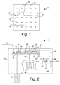
Fig. 1 is a graphical illustration of an example of a sensor node layout with respect to a geographic area overlying an earth surface; -
Fig. 2 is a schematic illustration of an embodiment of a sensor node of the present invention; and -
Fig. 3 is an illustration of a magnetic pick-up on a work machine which could be used to remove the non-biodegradable portions of sensor nodes from an earth surface. - Referring now to the drawings, and more particularly to
Fig. 1 , there is shown a graphical illustration of awireless network 10 of the present invention, including an example of a sensor node layout with respect to a geographic area overlying an earth surface.Wireless network 10 can be deployed over any suitable geographic area. For example, in the embodiment illustrated inFig. 1 ,wireless network 10 is assumed to be deployed in an agricultural field. As another example,wireless network 10 could be deployed for natural resource management and a geographic area could represent, e.g., a large forested area. Other applications are also possible. -
Wireless network 10 includes a plurality of sensor nodes 12 (designated generally with a "+" sign) which are deployed in association withearth surface 14.Contour lines 16 are simply intended to show variances in topography, but could also represent variances in soil type, work versus non-work areas, etc. It will be appreciated that the particular layout ofsensor nodes 12, such as spacing, pattern, deployment depth, etc. can vary from one application to another. - Each
sensor node 12 is deployed in association withearth surface 14, broadly meaning thatsensor nodes 12 could be deployed at any level within the earth surface, partially within the earth surface, or on top of the earth surface. The term "earth surface" is also broadly intended to cover any type of surface or material, such as soil, compost, sludge, manure, cellulosic materials such as stover, bagasse, wood chips, etc. - Referring now to
Fig. 2 , eachsensor node 12 generally includes a biodegradableplastic housing 18, anelectronic circuit board 20 withinhousing 18, and one or morenon-toxic batteries 22. -
Housing 18 is constructed from a biodegradable plastic which is selected and formed to last through the expected service life ofsensor node 12. An example of a plastic of this type is made by the former Cargill Dow, LLC from corn. Other examples of biodegradable plastics include polymeric and polyester materials of many specific types. Specific examples of such plastics include a polyhydroxyalkanoate (PHA) polymer, poly(3-hydroxybutyrate) (P3HB) polyester, polyhydroxyalkanoates, poly(k-caprolactone), poly(I-lactide), and both aliphatic and aromatic polyalkylene dicarboxylic acids. -
Circuit board 20 includes a non-toxic, preferablybiodegradable substrate 24 and one or more lead-free solder elements 26.Substrate 24 can be formed from a suitable biodegradable material having sufficient dielectric properties.Substrate 24 can be a single layer substrate or a multi-layer substrate with solder runs between the various layers. It may be possible, e.g., to formsubstrate 24 from a non-hydrocarbon based plastic as described above with reference to the material types ofhousing 18. -
Solder elements 26 are intended generally to cover any type of lead-free solder feature onboard or withincircuit board 20. For example,solder elements 26 can be in the form of solder runs or solder pads carried bycircuit board 20. -
Circuit board 20 also includes a plurality ofelectronic components 28 which are carried bysubstrate 24.Electronic components 28 may be of any suitable type for the specific application, and can be of the surface mount (smt) type or leaded type. In the embodiment shown inFig. 2 ,electronic components 28 are illustrated as includingleads 30, which are preferably gold plated to prevent oxidation. - In the event that
electronic components 28 are themselves not biodegradable, anencapsulation 32 may be provided aroundelectronic components 28.Encapsulation 32 is formed from a material which is an environmentally friendly, non-degrading and durable material. For example,encapsulation 32 can be formed from glass or specific types of potting compounds. Additionally, theelectronic components 28 can be encapsulated with a single encapsulation, or encapsulated for different geographic areas oncircuit board 20, as shown inFig. 2 . - In one example, an
electronic component 28 can be in the form of an integrated circuit (IC) formed from a non-degrading durable material such as a suitable ceramic material. The IC may include external leads which are physically held against or metallurgically bonded to solder pads on thecircuit board 20, with the IC being encapsulated with a biodegradable potting material. The circuit board can of course also carry other suitable electronic components, such as an RF transceiver, etc. -
Encapsulation 32 can optionally include a magnetic material which is associated therewith.
In the event that theelectronic components 28 are not biodegradable, the magnetic material allows the encapsulated electronic components to be removed from the earth surface using a suitable magnet. For example, referring toFig. 3 , in the case wheresensor nodes 12 are deployed within an agricultural field, astrong magnet 34 carried by atractor 36 can be used to remove eachencapsulation 32 havingelectronic components 28 embedded therein. In the embodiment ofencapsulation 32 shown inFig. 2 , magnetic particles 38 (shown in enlarged form in one of the encapsulations) are entrained within theencapsulation 32 for possible subsequent retrieval using a magnetic pick-up on a work machine or the like. It is also possible that a magnetic plate (not shown), such as a steel plate, can be affixed to the outer surface ofencapsulation 32. -
Battery 22 can be of any suitable configuration, such as a flexible thin film battery, etc. In the embodiment shown inFig. 2 ,battery 22 generally includes a non-toxic case 40, a plurality ofnon-toxic electrodes 42 within case 40, and anon-toxic electrolyte 44. Case 40 is preferably also biodegradable in addition to being non-toxic, and can be formed from a biodegradable plastic as described above with reference tohousing 18.Electrolyte 44 is a non-toxic, naturally originated acid such as citric acid or ascetic acid.Electrolyte 44 will thus not harm the environment upon biodegradation of case 40. - In the embodiment shown,
electrolyte 44 is in contact withelectrodes 42. It is also possible to providebattery 22 with an internalbiodegradable membrane 46 which separates the electrolyte from at least one of the plurality of electrodes 42 (shown in dashed line as an optional feature inFig. 2 ). For example,electrolyte 44 could be positioned on one side ofmembrane 46 and in contact with only one of theelectrodes 42. Rupturing the membrane 46 (such as through an electrolyte fill hole), as shown schematically atreference 46A, for "just-in-time" use would causeelectrolyte 44 to flow across case 40 to contact bothelectrodes 42. Alternatively, it may be possible to move therightmost electrode 44 shown inFig. 2 to the position shown by dashedline 48, such that both electrodes are not in contact withelectrolyte 44 untilmembrane 46 is ruptured by a user. As yet a further example, it may be possible to place water on one side ofmembrane 46 and salts on the opposite side ofmembrane 46, wherein mixing of the water and salts occurs upon rupturing ofmembrane 46 to form the electrolyte. -
Battery 22 may be electrically coupled withcircuit board 20 usingnon-toxic conductors 50, such as copper or aluminum conductors.Conductors 50 may also be in the form of a conductive non-toxic ink which electrically connects betweenbattery 22 andcircuit board 20. - For example, the non-toxic ink can be in the form of traces which are formed from a soy-based ink with conductive particles.
-
Sensor node 12 also includes asensor 52 which is coupled withcircuit board 20.Sensor 52 may be any suitable type sensor for sensing a desired parameter associated withearth surface 14, such as a temperature sensor, moisture sensor, pH sensor, etc. -
Sensor node 12 further includes anantenna 54 which is affixed tohousing 18 and configured for use as an antenna for wireless communications. In the embodiment illustrated inFig. 2 ,antenna 54 is in the form of a conductive non-toxic ink which is printed onhousing 18 and connected to at least one of theelectronic components 28 onboard circuit board 20 (a portion ofhousing 18 is shown in fragmentary form inFig. 2 for purposes of illustration).Antenna 54 is shown with a folded configuration but may have any suitable size and shape.Antenna 54 preferably is a patch antenna carried byhousing 18, and formed from a thin sheet material, screened ink, etc. In the embodiment shown,antenna 54 is formed from a conductive non-toxic ink such as, e.g., a soy-based ink with conductive particles. -
Conductor 56 interconnectingantenna 54 with one or moreelectronic components 28onboard circuit board 20 may be a non-toxic conductor, such as an aluminum or copper conductor. Alternatively,conductor 56 may be a conductive non-toxic ink, such as a soy-based ink with conductive particles, as described above with reference toconductors 50. - During installation of
sensor nodes 12 withinwireless network 10, the sensor nodes may be manually or automatically placed in association withearth surface 14 at a desired deployment depth, spacing and pattern. The material type and configuration of the various components making up eachsensor node 12 are designed with a desired service life generally corresponding to an expected service life of the one ormore batteries 22. Most of the components making up eachsensor node 12 are preferably biodegradable and begin the biodegradation process after depletion of the one ormore batteries 22. In the event that one or more components associated withsensor node 12 are not biodegradable, such as perhapselectronic components 28, such components are designed to either be environmentally friendly or encapsulated within anencapsulation 32 to render them environmentally inert. In the event that the remainingencapsulation 32 includes or is attached to a magnetic material, thevarious encapsulations 32 may be picked up from the earth surface using a pick-upmagnet 34 of various types and configurations.
Claims (15)
- A sensor node (12) for deployment in association with an earth surface (14), said sensor node (12) comprising:a biodegradable plastic housing (18);an electronic circuit board (20) within said housing (18), said circuit board (20) having a non-toxic substrate (24) and at least one lead-free solder element (26); andat least one battery (22) for providing electrical energy to said circuit board (20), each said battery (22) being a non-toxic battery.
- The sensor node (12) of claim 1, wherein said circuit board (20) has a biodegradable substrate (24) with a plurality of electronic components (28) carried by said substrate.
- The sensor node (12) of claim 2, wherein each said electronic component (28) has a plurality of electrical leads (26), each said lead being gold plated.
- The sensor node (12) of claim 2, having a conductive non-toxic ink printed on said housing (18) and connected to at least one of said electronic components (28), said conductive non-toxic ink, for example a soy-based ink, having conductive particles and being configured for use as an antenna (54) for wireless communications.
- The sensor node (12) of claim 2, having a conductive non-toxic ink, especially a soy-based ink, for electrical connection between each said battery (22), said circuit board (20), and an antenna (54), the ink having conductive particles.
- The sensor node (12) of claim 2, having an encapsulation (32) around said electronic components (28), said encapsulation (32) formed from a non-degrading durable material.
- The sensor node (12) of claim 6, wherein said encapsulation (32) is one of a potting compound and glass.
- The sensor node (12) of claim 6, having a magnetic material (38) which is one of affixed to an outer surface of said encapsulation (32), and embedded within said encapsulation (32).
- The sensor node (12) of claim 1, wherein each said solder element (26) has one of a pad and a trace.
- The sensor node (12) of claim 1, wherein each said battery (22) has a non-toxic case (40), a plurality of non-toxic electrodes (42) within said case, and a non-toxic electrolyte (44), preferably a naturally originated acid, in particular consisting essentially of one of: citric acid and ascetic acid.
- The sensor node (12) of claim 10, wherein said electrolyte (44) is one of within said case (40), and separate from and installable within said case (40).
- The sensor node (12) of claim 10, wherein said battery (22) has a biodegradable membrane (46) separating said electrolyte (44) from at least some of said plurality of electrodes (42).
- The sensor node (12) of claim 10, wherein said battery case (40) is biodegradable.
- A wireless network (10) having a plurality of sensor nodes (12) according to one of the preceding claims deployed in association with an earth surface (14).
- A method of using a sensor node (12) which is suitable for use with a wireless network (10), comprising the steps of:deploying the sensor node (12) relative to an earth surface (14), the sensor node (12) having a biodegradable plastic housing (18), an electronic circuit board (20) having a non-toxic substrate (24) and at least one lead-free solder element (26), and a non-toxic battery (22) for providing electrical energy to the circuit board (20); andbiodegrading at least a portion of the sensor node (12).
Applications Claiming Priority (1)
| Application Number | Priority Date | Filing Date | Title |
|---|---|---|---|
| US12/133,643 US8063774B2 (en) | 2008-06-05 | 2008-06-05 | Non-toxic, biodegradable sensor nodes for use with a wireless network |
Publications (3)
| Publication Number | Publication Date |
|---|---|
| EP2131160A2 true EP2131160A2 (en) | 2009-12-09 |
| EP2131160A3 EP2131160A3 (en) | 2017-01-04 |
| EP2131160B1 EP2131160B1 (en) | 2019-05-15 |
Family
ID=41228282
Family Applications (1)
| Application Number | Title | Priority Date | Filing Date |
|---|---|---|---|
| EP09161836.3A Active EP2131160B1 (en) | 2008-06-05 | 2009-06-03 | Non-toxic, biodegradable sensor nodes for use with a wireless network |
Country Status (2)
| Country | Link |
|---|---|
| US (1) | US8063774B2 (en) |
| EP (1) | EP2131160B1 (en) |
Cited By (2)
| Publication number | Priority date | Publication date | Assignee | Title |
|---|---|---|---|---|
| CZ309063B6 (en) * | 2020-08-20 | 2022-01-05 | Univerzita Pardubice | System for measuring the temperature and humidity of air and soil with wireless data transmission and method of producing it |
| US12306129B2 (en) | 2020-08-20 | 2025-05-20 | Univerzita Pardubice | System for measuring temperature and moisture of air and soil with wireless data transmission and method of its production |
Families Citing this family (19)
| Publication number | Priority date | Publication date | Assignee | Title |
|---|---|---|---|---|
| US8706362B2 (en) * | 2010-10-22 | 2014-04-22 | Deere & Company | Mobile biological material energy conversion |
| CA2898182C (en) * | 2013-01-15 | 2017-07-11 | Ndsu Research Foundation | Biodegradable soil sensor, system and method |
| WO2015137922A1 (en) * | 2014-03-11 | 2015-09-17 | Empire Technology Development Llc | Biodegradable printed circuit boards |
| US10190894B2 (en) * | 2015-12-26 | 2019-01-29 | Intel Corporation | Technologies for controlling degradation of sensing circuits |
| US10831199B2 (en) | 2017-09-29 | 2020-11-10 | Deere & Company | Using unmanned aerial vehicles to provide ground control points for aerial survey |
| JP6897643B2 (en) * | 2018-09-05 | 2021-07-07 | 横河電機株式会社 | Sensor element and packaging |
| US11924730B2 (en) * | 2020-11-23 | 2024-03-05 | Micron Technology, Inc. | Operating emergency prevention sensor systems |
| DE102022200787A1 (en) | 2022-01-25 | 2023-07-27 | Fraunhofer-Gesellschaft zur Förderung der angewandten Forschung eingetragener Verein | Electronic sensor for recording an environmental parameter |
| US12382856B2 (en) | 2022-08-31 | 2025-08-12 | Deere & Company | Method for locating and planting sentinel plants |
| US12085993B2 (en) | 2022-10-18 | 2024-09-10 | Dell Products L.P. | Information handling system coupling device for improved assembly, disassembly and repair |
| US12306676B2 (en) | 2022-10-18 | 2025-05-20 | Dell Products L.P. | Information handling system keyboard with rapid assembly and disassembly to aid recycling |
| US11650671B1 (en) | 2022-10-18 | 2023-05-16 | Dell Products L.P. | Information handling system keyboard with rapid assembly and disassembly to aid recycling |
| US12596997B2 (en) | 2022-10-18 | 2026-04-07 | Dell Products L.P. | Information handling system and peripheral printed circuit board having non-homogeneous substrate material |
| US12273609B2 (en) | 2022-10-18 | 2025-04-08 | Dell Products L.P. | Camera sensor and lens housing structure for enhanced manufacture assembly and repair |
| US11856719B1 (en) | 2022-10-18 | 2023-12-26 | Dell Products L.P. | Information handling system mouse with rapid assembly and disassembly to aid recycling |
| US12245372B2 (en) | 2022-10-18 | 2025-03-04 | Dell Products L.P. | Information handling system and peripheral printed circuit board having non-homogeneous substrate material and integrated thermal solution |
| US12235683B2 (en) | 2022-10-18 | 2025-02-25 | Dell Products L.P. | Information handling system display rapid panel assembly and repair |
| US12306677B2 (en) | 2022-10-18 | 2025-05-20 | Dell Products L.P. | Information handling system with rapid assembly and disassembly to aid recycling |
| US12284429B2 (en) | 2022-10-18 | 2025-04-22 | Dell Products L.P. | Camera housing structure for enhanced manufacture assembly and repair |
Citations (1)
| Publication number | Priority date | Publication date | Assignee | Title |
|---|---|---|---|---|
| US20070039745A1 (en) | 2005-08-18 | 2007-02-22 | Deere & Company, A Delaware Corporation | Wireless subsoil sensor network |
Family Cites Families (28)
| Publication number | Priority date | Publication date | Assignee | Title |
|---|---|---|---|---|
| US4396149A (en) * | 1980-12-30 | 1983-08-02 | Energy Management Corporation | Irrigation control system |
| US5177660A (en) * | 1990-09-11 | 1993-01-05 | Sunclipse, Inc. | Biodegradable and recyclable electrostatically shielded packaging for electronic devices and media |
| US5277997A (en) * | 1992-07-30 | 1994-01-11 | Alupower, Inc. | Absorber assembly for alkali solutions |
| US5266422A (en) * | 1992-12-21 | 1993-11-30 | Board Of Trustees Operating Michigan State University | Branched polyhydroxyalkanoate polymer salt electrolytic compositions and method of preparation |
| US5395707A (en) * | 1993-05-07 | 1995-03-07 | Acr Electronics, Inc. | Environmentally safe water-activated battery |
| US5916710A (en) * | 1993-05-19 | 1999-06-29 | The Regents Of The University Of California | Sodium cobalt bronze batteries and a method for making same |
| US5495250A (en) * | 1993-11-01 | 1996-02-27 | Motorola, Inc. | Battery-powered RF tags and apparatus for manufacturing the same |
| DE19517863C2 (en) * | 1995-05-16 | 1998-10-22 | Metallgesellschaft Ag | Process for dry desulfurization of a combustion exhaust gas |
| US5589295A (en) * | 1995-12-06 | 1996-12-31 | Derzon; Dora K. | Thin film polymeric gel electrolytes |
| DE69710089T2 (en) * | 1996-08-16 | 2002-08-22 | Hugh P. Craig | PRINTABLE COMPOSITIONS AND THEIR APPLICATION ON DIELECTRIC SURFACES FOR THE PRODUCTION OF PRINTED CIRCUITS |
| US5718986A (en) * | 1996-09-17 | 1998-02-17 | Brenner; Abner | Cells with a battery positive of hypochlorite or chlorite ion and anodes of magnesium or aluminum |
| US5933765A (en) | 1996-10-08 | 1999-08-03 | Motorola, Inc. | Communication device having a reduced level of hazardous substances |
| US7122615B1 (en) * | 1998-09-10 | 2006-10-17 | Rutgers, The State University Of New Jersey | Polyanhydrides with therapeutically useful degradation products |
| GB2345196B (en) * | 1998-12-23 | 2003-11-26 | Nokia Mobile Phones Ltd | An antenna and method of production |
| WO2000074402A1 (en) | 1999-05-28 | 2000-12-07 | Afx Technology Group International, Inc. | Wireless transceiver network employing node-to-node data messaging |
| JP4345183B2 (en) * | 1999-12-20 | 2009-10-14 | ソニー株式会社 | Electric appliances |
| US6975245B1 (en) * | 2000-09-18 | 2005-12-13 | Battelle Energy Alliance, Llc | Real-time data acquisition and telemetry based irrigation control system |
| US7003405B1 (en) * | 2001-10-25 | 2006-02-21 | Sandia Corporation | Methods for characterizing subsurface volatile contaminants using in-situ sensors |
| CN1296432C (en) | 2002-03-29 | 2007-01-24 | 三井化学株式会社 | Lactic acid-based resin composition |
| US20030182841A1 (en) * | 2002-03-30 | 2003-10-02 | Calak Charles Thomas | Disposable illuminated fishing lure |
| EP1562456A2 (en) * | 2002-11-08 | 2005-08-17 | Colgate-Palmolive Company | Toothbrush assembly having an environmentally safe polymer battery |
| US8097273B2 (en) | 2003-04-10 | 2012-01-17 | Teijin Limited | Biodegradable film having honeycomb structure |
| AU2003902836A0 (en) * | 2003-06-06 | 2003-06-26 | M.B.T.L. Limited | Environmental sensor |
| US7370119B2 (en) * | 2004-05-21 | 2008-05-06 | Cisco Technology, Inc. | Scalable MPLS fast reroute switchover with reduced complexity |
| US20060080819A1 (en) * | 2004-09-14 | 2006-04-20 | Mcallister Clarke W | Systems and methods for deployment and recycling of RFID tags, wireless sensors, and the containers attached thereto |
| JP4359577B2 (en) * | 2005-06-16 | 2009-11-04 | 富士フイルム株式会社 | Black and white photothermographic material |
| JP2007106783A (en) * | 2005-10-11 | 2007-04-26 | Fujitsu Ltd | RESIN MOLDED BODY, ELECTRONIC DEVICE USING THE SAME, AND METHOD FOR TREATING RESIN MOLDED BODY |
| US7318010B2 (en) * | 2006-02-07 | 2008-01-08 | Deere & Company | Method of regulating wireless sensor network energy use |
-
2008
- 2008-06-05 US US12/133,643 patent/US8063774B2/en active Active
-
2009
- 2009-06-03 EP EP09161836.3A patent/EP2131160B1/en active Active
Patent Citations (1)
| Publication number | Priority date | Publication date | Assignee | Title |
|---|---|---|---|---|
| US20070039745A1 (en) | 2005-08-18 | 2007-02-22 | Deere & Company, A Delaware Corporation | Wireless subsoil sensor network |
Cited By (2)
| Publication number | Priority date | Publication date | Assignee | Title |
|---|---|---|---|---|
| CZ309063B6 (en) * | 2020-08-20 | 2022-01-05 | Univerzita Pardubice | System for measuring the temperature and humidity of air and soil with wireless data transmission and method of producing it |
| US12306129B2 (en) | 2020-08-20 | 2025-05-20 | Univerzita Pardubice | System for measuring temperature and moisture of air and soil with wireless data transmission and method of its production |
Also Published As
| Publication number | Publication date |
|---|---|
| EP2131160B1 (en) | 2019-05-15 |
| US8063774B2 (en) | 2011-11-22 |
| EP2131160A3 (en) | 2017-01-04 |
| US20090303071A1 (en) | 2009-12-10 |
Similar Documents
| Publication | Publication Date | Title |
|---|---|---|
| US8063774B2 (en) | Non-toxic, biodegradable sensor nodes for use with a wireless network | |
| US6421013B1 (en) | Tamper-resistant wireless article including an antenna | |
| US6353420B1 (en) | Wireless article including a plural-turn loop antenna | |
| US20120195018A1 (en) | Wireless communication device using voltage switchable dielectric material | |
| EP2705735B1 (en) | Method for manufacturing printed circuit board | |
| US8284117B2 (en) | Antenna device and method of manufacturing the same | |
| AU2015285996B2 (en) | Sensor device having a flexible electrical conductor structure | |
| JP2007311092A (en) | Printed wiring board assembly and method for manufacturing the printed wiring board assembly | |
| EP1995999A3 (en) | Circuitized substrate with conductive paste, electrical assembly including said circuitized substrate and method of making said substrate | |
| EP1724714A2 (en) | Patch antenna for RFID tag | |
| EP2259213A3 (en) | RFID device | |
| EP1581037A3 (en) | Method of manufacturing a sealed electronic module | |
| EP1970722A3 (en) | Protection Circuit Board for Secondary Battery | |
| WO2009001621A1 (en) | Manufacturing method for part built-in substrate | |
| JP2021534596A (en) | Structure with deformable conductor | |
| EP1976349A3 (en) | Circuitized substrate with internal organic memory device, method of making same, electrical assembly utilizing same, and information handling system utilizing same | |
| EP1953821A3 (en) | Semiconductor package substrate | |
| EP1069811A3 (en) | Multi-layer wiring board and method for manufacturing the same | |
| EP1976060A4 (en) | INTEGRATED ANTENNA MODULE, CARD-TYPE INFORMATION DEVICE AND METHODS OF MAKING SAME | |
| US20100264225A1 (en) | Wireless communication device using voltage switchable dielectric material | |
| EP1394856A3 (en) | Surface-mounted electronic component module and method for manufacturing the same | |
| CN102480850A (en) | Method for installing RFID electronic tags on printed circuit boards | |
| WO2005018292A3 (en) | Selective application of conductive material to circuit boards by pick and place | |
| WO2009054236A1 (en) | Planar antenna and method for manufacturing the same | |
| DE102010028868B4 (en) | Semiconductor substrate-based arrangement for an RFID device, RFID device and method for producing such a semiconductor substrate-based arrangement |
Legal Events
| Date | Code | Title | Description |
|---|---|---|---|
| PUAI | Public reference made under article 153(3) epc to a published international application that has entered the european phase |
Free format text: ORIGINAL CODE: 0009012 |
|
| AK | Designated contracting states |
Kind code of ref document: A2 Designated state(s): AT BE BG CH CY CZ DE DK EE ES FI FR GB GR HR HU IE IS IT LI LT LU LV MC MK MT NL NO PL PT RO SE SI SK TR |
|
| PUAL | Search report despatched |
Free format text: ORIGINAL CODE: 0009013 |
|
| AK | Designated contracting states |
Kind code of ref document: A3 Designated state(s): AT BE BG CH CY CZ DE DK EE ES FI FR GB GR HR HU IE IS IT LI LT LU LV MC MK MT NL NO PL PT RO SE SI SK TR |
|
| AX | Request for extension of the european patent |
Extension state: AL BA RS |
|
| RIC1 | Information provided on ipc code assigned before grant |
Ipc: G01D 11/24 20060101AFI20161130BHEP Ipc: H05K 1/02 20060101ALI20161130BHEP Ipc: H05K 1/03 20060101ALI20161130BHEP |
|
| STAA | Information on the status of an ep patent application or granted ep patent |
Free format text: STATUS: REQUEST FOR EXAMINATION WAS MADE |
|
| 17P | Request for examination filed |
Effective date: 20170704 |
|
| RBV | Designated contracting states (corrected) |
Designated state(s): AT BE BG CH CY CZ DE DK EE ES FI FR GB GR HR HU IE IS IT LI LT LU LV MC MK MT NL NO PL PT RO SE SI SK TR |
|
| STAA | Information on the status of an ep patent application or granted ep patent |
Free format text: STATUS: EXAMINATION IS IN PROGRESS |
|
| 17Q | First examination report despatched |
Effective date: 20170830 |
|
| GRAP | Despatch of communication of intention to grant a patent |
Free format text: ORIGINAL CODE: EPIDOSNIGR1 |
|
| STAA | Information on the status of an ep patent application or granted ep patent |
Free format text: STATUS: GRANT OF PATENT IS INTENDED |
|
| INTG | Intention to grant announced |
Effective date: 20181204 |
|
| GRAS | Grant fee paid |
Free format text: ORIGINAL CODE: EPIDOSNIGR3 |
|
| GRAA | (expected) grant |
Free format text: ORIGINAL CODE: 0009210 |
|
| STAA | Information on the status of an ep patent application or granted ep patent |
Free format text: STATUS: THE PATENT HAS BEEN GRANTED |
|
| AK | Designated contracting states |
Kind code of ref document: B1 Designated state(s): AT BE BG CH CY CZ DE DK EE ES FI FR GB GR HR HU IE IS IT LI LT LU LV MC MK MT NL NO PL PT RO SE SI SK TR |
|
| REG | Reference to a national code |
Ref country code: CH Ref legal event code: EP Ref country code: GB Ref legal event code: FG4D |
|
| REG | Reference to a national code |
Ref country code: DE Ref legal event code: R096 Ref document number: 602009058333 Country of ref document: DE |
|
| REG | Reference to a national code |
Ref country code: IE Ref legal event code: FG4D |
|
| REG | Reference to a national code |
Ref country code: NL Ref legal event code: MP Effective date: 20190515 |
|
| REG | Reference to a national code |
Ref country code: LT Ref legal event code: MG4D |
|
| PG25 | Lapsed in a contracting state [announced via postgrant information from national office to epo] |
Ref country code: ES Free format text: LAPSE BECAUSE OF FAILURE TO SUBMIT A TRANSLATION OF THE DESCRIPTION OR TO PAY THE FEE WITHIN THE PRESCRIBED TIME-LIMIT Effective date: 20190515 Ref country code: LT Free format text: LAPSE BECAUSE OF FAILURE TO SUBMIT A TRANSLATION OF THE DESCRIPTION OR TO PAY THE FEE WITHIN THE PRESCRIBED TIME-LIMIT Effective date: 20190515 Ref country code: HR Free format text: LAPSE BECAUSE OF FAILURE TO SUBMIT A TRANSLATION OF THE DESCRIPTION OR TO PAY THE FEE WITHIN THE PRESCRIBED TIME-LIMIT Effective date: 20190515 Ref country code: NL Free format text: LAPSE BECAUSE OF FAILURE TO SUBMIT A TRANSLATION OF THE DESCRIPTION OR TO PAY THE FEE WITHIN THE PRESCRIBED TIME-LIMIT Effective date: 20190515 Ref country code: SE Free format text: LAPSE BECAUSE OF FAILURE TO SUBMIT A TRANSLATION OF THE DESCRIPTION OR TO PAY THE FEE WITHIN THE PRESCRIBED TIME-LIMIT Effective date: 20190515 Ref country code: NO Free format text: LAPSE BECAUSE OF FAILURE TO SUBMIT A TRANSLATION OF THE DESCRIPTION OR TO PAY THE FEE WITHIN THE PRESCRIBED TIME-LIMIT Effective date: 20190815 Ref country code: FI Free format text: LAPSE BECAUSE OF FAILURE TO SUBMIT A TRANSLATION OF THE DESCRIPTION OR TO PAY THE FEE WITHIN THE PRESCRIBED TIME-LIMIT Effective date: 20190515 Ref country code: PT Free format text: LAPSE BECAUSE OF FAILURE TO SUBMIT A TRANSLATION OF THE DESCRIPTION OR TO PAY THE FEE WITHIN THE PRESCRIBED TIME-LIMIT Effective date: 20190915 |
|
| PG25 | Lapsed in a contracting state [announced via postgrant information from national office to epo] |
Ref country code: LV Free format text: LAPSE BECAUSE OF FAILURE TO SUBMIT A TRANSLATION OF THE DESCRIPTION OR TO PAY THE FEE WITHIN THE PRESCRIBED TIME-LIMIT Effective date: 20190515 Ref country code: BG Free format text: LAPSE BECAUSE OF FAILURE TO SUBMIT A TRANSLATION OF THE DESCRIPTION OR TO PAY THE FEE WITHIN THE PRESCRIBED TIME-LIMIT Effective date: 20190815 Ref country code: GR Free format text: LAPSE BECAUSE OF FAILURE TO SUBMIT A TRANSLATION OF THE DESCRIPTION OR TO PAY THE FEE WITHIN THE PRESCRIBED TIME-LIMIT Effective date: 20190816 |
|
| REG | Reference to a national code |
Ref country code: AT Ref legal event code: MK05 Ref document number: 1133986 Country of ref document: AT Kind code of ref document: T Effective date: 20190515 |
|
| PG25 | Lapsed in a contracting state [announced via postgrant information from national office to epo] |
Ref country code: CZ Free format text: LAPSE BECAUSE OF FAILURE TO SUBMIT A TRANSLATION OF THE DESCRIPTION OR TO PAY THE FEE WITHIN THE PRESCRIBED TIME-LIMIT Effective date: 20190515 Ref country code: SK Free format text: LAPSE BECAUSE OF FAILURE TO SUBMIT A TRANSLATION OF THE DESCRIPTION OR TO PAY THE FEE WITHIN THE PRESCRIBED TIME-LIMIT Effective date: 20190515 Ref country code: EE Free format text: LAPSE BECAUSE OF FAILURE TO SUBMIT A TRANSLATION OF THE DESCRIPTION OR TO PAY THE FEE WITHIN THE PRESCRIBED TIME-LIMIT Effective date: 20190515 Ref country code: DK Free format text: LAPSE BECAUSE OF FAILURE TO SUBMIT A TRANSLATION OF THE DESCRIPTION OR TO PAY THE FEE WITHIN THE PRESCRIBED TIME-LIMIT Effective date: 20190515 Ref country code: RO Free format text: LAPSE BECAUSE OF FAILURE TO SUBMIT A TRANSLATION OF THE DESCRIPTION OR TO PAY THE FEE WITHIN THE PRESCRIBED TIME-LIMIT Effective date: 20190515 Ref country code: AT Free format text: LAPSE BECAUSE OF FAILURE TO SUBMIT A TRANSLATION OF THE DESCRIPTION OR TO PAY THE FEE WITHIN THE PRESCRIBED TIME-LIMIT Effective date: 20190515 |
|
| REG | Reference to a national code |
Ref country code: CH Ref legal event code: PL |
|
| REG | Reference to a national code |
Ref country code: DE Ref legal event code: R097 Ref document number: 602009058333 Country of ref document: DE |
|
| PG25 | Lapsed in a contracting state [announced via postgrant information from national office to epo] |
Ref country code: MC Free format text: LAPSE BECAUSE OF FAILURE TO SUBMIT A TRANSLATION OF THE DESCRIPTION OR TO PAY THE FEE WITHIN THE PRESCRIBED TIME-LIMIT Effective date: 20190515 Ref country code: IT Free format text: LAPSE BECAUSE OF FAILURE TO SUBMIT A TRANSLATION OF THE DESCRIPTION OR TO PAY THE FEE WITHIN THE PRESCRIBED TIME-LIMIT Effective date: 20190515 |
|
| PLBE | No opposition filed within time limit |
Free format text: ORIGINAL CODE: 0009261 |
|
| STAA | Information on the status of an ep patent application or granted ep patent |
Free format text: STATUS: NO OPPOSITION FILED WITHIN TIME LIMIT |
|
| REG | Reference to a national code |
Ref country code: BE Ref legal event code: MM Effective date: 20190630 |
|
| PG25 | Lapsed in a contracting state [announced via postgrant information from national office to epo] |
Ref country code: TR Free format text: LAPSE BECAUSE OF FAILURE TO SUBMIT A TRANSLATION OF THE DESCRIPTION OR TO PAY THE FEE WITHIN THE PRESCRIBED TIME-LIMIT Effective date: 20190515 |
|
| 26N | No opposition filed |
Effective date: 20200218 |
|
| PG25 | Lapsed in a contracting state [announced via postgrant information from national office to epo] |
Ref country code: IE Free format text: LAPSE BECAUSE OF NON-PAYMENT OF DUE FEES Effective date: 20190603 Ref country code: PL Free format text: LAPSE BECAUSE OF FAILURE TO SUBMIT A TRANSLATION OF THE DESCRIPTION OR TO PAY THE FEE WITHIN THE PRESCRIBED TIME-LIMIT Effective date: 20190515 |
|
| PG25 | Lapsed in a contracting state [announced via postgrant information from national office to epo] |
Ref country code: CH Free format text: LAPSE BECAUSE OF NON-PAYMENT OF DUE FEES Effective date: 20190630 Ref country code: LU Free format text: LAPSE BECAUSE OF NON-PAYMENT OF DUE FEES Effective date: 20190603 Ref country code: LI Free format text: LAPSE BECAUSE OF NON-PAYMENT OF DUE FEES Effective date: 20190630 Ref country code: BE Free format text: LAPSE BECAUSE OF NON-PAYMENT OF DUE FEES Effective date: 20190630 Ref country code: SI Free format text: LAPSE BECAUSE OF FAILURE TO SUBMIT A TRANSLATION OF THE DESCRIPTION OR TO PAY THE FEE WITHIN THE PRESCRIBED TIME-LIMIT Effective date: 20190515 |
|
| PG25 | Lapsed in a contracting state [announced via postgrant information from national office to epo] |
Ref country code: FR Free format text: LAPSE BECAUSE OF NON-PAYMENT OF DUE FEES Effective date: 20190715 |
|
| PG25 | Lapsed in a contracting state [announced via postgrant information from national office to epo] |
Ref country code: CY Free format text: LAPSE BECAUSE OF FAILURE TO SUBMIT A TRANSLATION OF THE DESCRIPTION OR TO PAY THE FEE WITHIN THE PRESCRIBED TIME-LIMIT Effective date: 20190515 |
|
| PG25 | Lapsed in a contracting state [announced via postgrant information from national office to epo] |
Ref country code: IS Free format text: LAPSE BECAUSE OF FAILURE TO SUBMIT A TRANSLATION OF THE DESCRIPTION OR TO PAY THE FEE WITHIN THE PRESCRIBED TIME-LIMIT Effective date: 20190915 |
|
| PG25 | Lapsed in a contracting state [announced via postgrant information from national office to epo] |
Ref country code: HU Free format text: LAPSE BECAUSE OF FAILURE TO SUBMIT A TRANSLATION OF THE DESCRIPTION OR TO PAY THE FEE WITHIN THE PRESCRIBED TIME-LIMIT; INVALID AB INITIO Effective date: 20090603 Ref country code: MT Free format text: LAPSE BECAUSE OF FAILURE TO SUBMIT A TRANSLATION OF THE DESCRIPTION OR TO PAY THE FEE WITHIN THE PRESCRIBED TIME-LIMIT Effective date: 20190515 |
|
| PG25 | Lapsed in a contracting state [announced via postgrant information from national office to epo] |
Ref country code: MK Free format text: LAPSE BECAUSE OF FAILURE TO SUBMIT A TRANSLATION OF THE DESCRIPTION OR TO PAY THE FEE WITHIN THE PRESCRIBED TIME-LIMIT Effective date: 20190515 |
|
| PGFP | Annual fee paid to national office [announced via postgrant information from national office to epo] |
Ref country code: DE Payment date: 20250521 Year of fee payment: 17 |
|
| PGFP | Annual fee paid to national office [announced via postgrant information from national office to epo] |
Ref country code: GB Payment date: 20250627 Year of fee payment: 17 |